EP1876648B1 - Method and apparatus for increasing light absorption in an image sensor using energy conversion layer - Google Patents
Method and apparatus for increasing light absorption in an image sensor using energy conversion layer Download PDFInfo
- Publication number
- EP1876648B1 EP1876648B1 EP07111760.0A EP07111760A EP1876648B1 EP 1876648 B1 EP1876648 B1 EP 1876648B1 EP 07111760 A EP07111760 A EP 07111760A EP 1876648 B1 EP1876648 B1 EP 1876648B1
- Authority
- EP
- European Patent Office
- Prior art keywords
- color filter
- layer
- color
- energy conversion
- light
- Prior art date
- Legal status (The legal status is an assumption and is not a legal conclusion. Google has not performed a legal analysis and makes no representation as to the accuracy of the status listed.)
- Active
Links
Images


Classifications
-
- H—ELECTRICITY
- H10—SEMICONDUCTOR DEVICES; ELECTRIC SOLID-STATE DEVICES NOT OTHERWISE PROVIDED FOR
- H10F—INORGANIC SEMICONDUCTOR DEVICES SENSITIVE TO INFRARED RADIATION, LIGHT, ELECTROMAGNETIC RADIATION OF SHORTER WAVELENGTH OR CORPUSCULAR RADIATION
- H10F39/00—Integrated devices, or assemblies of multiple devices, comprising at least one element covered by group H10F30/00, e.g. radiation detectors comprising photodiode arrays
- H10F39/80—Constructional details of image sensors
- H10F39/806—Optical elements or arrangements associated with the image sensors
-
- H—ELECTRICITY
- H10—SEMICONDUCTOR DEVICES; ELECTRIC SOLID-STATE DEVICES NOT OTHERWISE PROVIDED FOR
- H10F—INORGANIC SEMICONDUCTOR DEVICES SENSITIVE TO INFRARED RADIATION, LIGHT, ELECTROMAGNETIC RADIATION OF SHORTER WAVELENGTH OR CORPUSCULAR RADIATION
- H10F39/00—Integrated devices, or assemblies of multiple devices, comprising at least one element covered by group H10F30/00, e.g. radiation detectors comprising photodiode arrays
- H10F39/10—Integrated devices
- H10F39/12—Image sensors
- H10F39/18—Complementary metal-oxide-semiconductor [CMOS] image sensors; Photodiode array image sensors
- H10F39/189—X-ray, gamma-ray or corpuscular radiation imagers
- H10F39/1898—Indirect radiation image sensors, e.g. using luminescent members
-
- H—ELECTRICITY
- H10—SEMICONDUCTOR DEVICES; ELECTRIC SOLID-STATE DEVICES NOT OTHERWISE PROVIDED FOR
- H10F—INORGANIC SEMICONDUCTOR DEVICES SENSITIVE TO INFRARED RADIATION, LIGHT, ELECTROMAGNETIC RADIATION OF SHORTER WAVELENGTH OR CORPUSCULAR RADIATION
- H10F39/00—Integrated devices, or assemblies of multiple devices, comprising at least one element covered by group H10F30/00, e.g. radiation detectors comprising photodiode arrays
- H10F39/80—Constructional details of image sensors
- H10F39/805—Coatings
- H10F39/8053—Colour filters
-
- H—ELECTRICITY
- H10—SEMICONDUCTOR DEVICES; ELECTRIC SOLID-STATE DEVICES NOT OTHERWISE PROVIDED FOR
- H10F—INORGANIC SEMICONDUCTOR DEVICES SENSITIVE TO INFRARED RADIATION, LIGHT, ELECTROMAGNETIC RADIATION OF SHORTER WAVELENGTH OR CORPUSCULAR RADIATION
- H10F39/00—Integrated devices, or assemblies of multiple devices, comprising at least one element covered by group H10F30/00, e.g. radiation detectors comprising photodiode arrays
- H10F39/80—Constructional details of image sensors
- H10F39/806—Optical elements or arrangements associated with the image sensors
- H10F39/8063—Microlenses
Definitions
- This disclosure relates generally to image sensors, and in particular but not exclusively, relates to image sensors with increased light absorption efficiency.
- Document JP2004207285 discloses an imaging device comprising a colour filter array and a wavelength conversion film.
- CMOS image sensor comprising:
- a system and method are disclosed herein for applying a layer of material (an energy conversion layer) in the image sensor fabrication process in order to increase the absorption of a specific range of the light spectrum by the image sensor.
- the energy conversion layer converts light rays from higher energy ranges (shorter wavelength) to lower energy ranges (longer wavelength) such that the light absorption by the image sensor can be increased.
- Some examples of energy conversion layers are YAG:Ce crystals or a crystalline cesium iodide scintillator or a rare-earth scintillator (e.g., terbium-doped gadolinium dioxide sulfide).
- the energy conversion layer may be composed of material that converts blue light to red light, and/or blue light to yellow light, and/or blue light to green light.
- the energy conversion layer is used with a color filter to increase the absorption of a specific range of the light spectrum.
- the energy conversion layer may be masked and deposited such that only filtered light of short wavelengths passes through the energy conversion layer, and filtered light of long wavelengths does not pass through the energy conversion layer.
- FIG. 1 is a cross-sectional view of a portion of a prior art CMOS Image sensor 100 with an RGB color filter layer 150. Three adjacent pixels are shown to illustrate a red (R), a green (G), and a blue (B) pixels formed in a photodiode layer 110.
- the CMOS image sensor 100 comprises the photodiode layer 110, a passivation layer 120 with embedded metal interconnects 130, a planarization layer 140, the RGB color filter layer 150, a spacer layer 160, and micro-lenses 170.
- FIG. 2 is a cross-sectional view of a portion of a CMOS image Sensor 200 with an energy conversion layer 250 formed underneath a blue section of an RGB color filter layer 260, in accordance with an embodiment of the invention.
- the energy conversion layer 250 need not be directly under the blue section (B) of the color filter 260, but may be formed further down in the stack, and as one example, may be formed in the passivation layer 220 or just above the photodiode layer 210. Similar to the prior art of FIG.
- the CMOS image sensor 200 comprises the photodiode layer 210, the passivation layer 220 with embedded metal interconnect structures 230, a planarization layer 240, RGB color filter layer 260, spacer layer 270, and micro-lenses 280.
- This embodiment of the present invention further adds the energy conversion layer 250.
- the energy conversion layer 250 is operative in this embodiment to convert the incident light passing through the blue filter (B) into light having a wavelength more readily sensed by the underlying photodiode in the photodiode layer 210.
- the visible light passing through the blue filter (B) would be at the blue wavelengths. These wavelengths are typically more difficult to detect by conventional photodiodes that are also used to detect red and green wavelengths.
- the energy conversion layer 250 in one embodiment could be a material that can convert blue wavelength light into red and/or yellow and/or green wavelength light.
- FIG. 3 is a cross-sectional view of a portion of a CMOS image sensor 300 with an energy conversion layer 350 formed between a spacer layer 360 and a planarization layer 340.
- the CMOS image sensor 300 comprises a photodiode layer 310, a passivation layer 320 with embedded metal interconnects 330, the planarization layer 340, the energy conversion layer 350, the spacer layer 360, and micro-lenses 370. Note that in this arrangement, a color filter layer is not present. Thus, the image sensor 300 is adapted for "black and white" (gray scale) imaging.
- the energy conversion layer 350 may be, for example, a layer that can convert incident x-rays into light wavelengths that can be easily detected by the photodiodes in the photodiode layer 310.
- An image sensor formed in accordance with FIG. 3 can then be used to image medical x-rays easily.
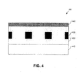
- FIG. 4 illustrates in cross-section a portion of a CMOS image sensor 400 with an energy conversion layer 440 placed on top of a passivation layer 420.
- the CMOS image sensor 400 comprises a photodiode layer 410, a passivation layer 420 with embedded metal interconnects 430, and an energy conversion layer 440.
Landscapes
- Solid State Image Pick-Up Elements (AREA)
Description
- This disclosure relates generally to image sensors, and in particular but not exclusively, relates to image sensors with increased light absorption efficiency.
- In the current art, image sensors lack efficiency in absorbing light having higher energy wavelengths. For example, light with red wavelengths is more efficiently absorbed than light having blue wavelengths. Document
JP2004207285 - Non-limiting and non-exhaustive embodiments of the invention are described with reference to the following figures, wherein like reference numerals refer to like parts throughout the various views unless otherwise specified.
-
FIG. 1 is a cross-sectional view of a portion of a prior art CMOS image sensor with an RGB color filter. -
FIG. 2 is a cross-sectional view of a portion of a CMOS image sensor with an energy conversion layer formed underneath a blue section of an RGB color filter layer, in accordance with an embodiment of the invention. -
FIG. 3 is a cross-sectional view of a portion of a CMOS image sensor with an energy conversion layer formed between a spacer layer and a planarization layer. -
FIG. 4 is a cross-sectional view of a portion of a CMOS image sensor with an energy conversion layer formed on top of a passivation layer. - According to the present invention there is a method, comprising:
- providing a color filter layer including a first color filter and a second color filter, wherein the first color filter and the second color filter are different color filters;
- passing electromagnetic radiation having a first wavelength range through the first color filter of the color filter layer of a Complementary Metal Oxide Semiconductor (CMOS) image sensor;
- receiving the electromagnetic radiation having the first wavelength range at an energy conversion layer of the CMOS image sensor;
- converting the electromagnetic radiation into electromagnetic radiation having a second wavelength range;
- directing the electromagnetic radiation having the second wavelength range from the energy conversion layer through a passivation layer;
- sensing the electromagnetic radiation having the second wavelength range at a photodiode layer; and
- routing an electrical signal via an interconnect structure formed within the passivation layer, the method being characterized in that
- the energy conversion layer is disposed directly under the color filter.
- According to a second aspect of the present invention there is a CMOS image sensor, comprising:
- a color filter layer to receive light, wherein the color filter layer includes a first and a second color filter, the first color filter and the second color filter are different color filters, the first color filter to allow light of substantially only a first color to pass through the first color filter;
- an energy conversion layer to receive the light of the first color and to convert the light of the first color into light of a second color;
- a passivation layer, having at least one metal interconnect formed therein; and
- a photodiode layer disposed to receive the light of the second color and to detect the received light of the second color, wherein the energy conversion layer and the passivation layer are disposed between the color filter layer and the photodiode layer;
- the sensor being characterized in that the energy conversion layer is disposed directly under the first color filter.
- In the following description numerous specific details are set forth to provide a thorough understanding of the embodiments. One skilled in the relevant art will recognize, however, that the techniques described herein can be practiced without one or more of the specific details, or with other methods, components, materials, etc. In other instances, well-known structures, materials, or operations are not shown or described in detail to avoid obscuring certain aspects.
- Reference throughout this specification to "one embodiment" or "an embodiment" means that a particular feature, structure, or characteristic described in connection with the embodiment is included in at least one embodiment of the present invention. Thus, the appearances of the phrases "in one embodiment" or "in an embodiment" in various places throughout this specification are not necessarily all referring to the same embodiment. Furthermore, the particular features, structures, or characteristics may be combined in any suitable manner in one or more embodiments.
- In general a system and method are disclosed herein for applying a layer of material (an energy conversion layer) in the image sensor fabrication process in order to increase the absorption of a specific range of the light spectrum by the image sensor. The energy conversion layer converts light rays from higher energy ranges (shorter wavelength) to lower energy ranges (longer wavelength) such that the light absorption by the image sensor can be increased. Some examples of energy conversion layers are YAG:Ce crystals or a crystalline cesium iodide scintillator or a rare-earth scintillator (e.g., terbium-doped gadolinium dioxide sulfide).
- In the embodiments of the invention, the energy conversion layer may be composed of material that converts blue light to red light, and/or blue light to yellow light, and/or blue light to green light.
- In one embodiment of the invention, the energy conversion layer is used with a color filter to increase the absorption of a specific range of the light spectrum. The energy conversion layer may be masked and deposited such that only filtered light of short wavelengths passes through the energy conversion layer, and filtered light of long wavelengths does not pass through the energy conversion layer.
-
FIG. 1 is a cross-sectional view of a portion of a prior artCMOS Image sensor 100 with an RGBcolor filter layer 150. Three adjacent pixels are shown to illustrate a red (R), a green (G), and a blue (B) pixels formed in aphotodiode layer 110. TheCMOS image sensor 100 comprises thephotodiode layer 110, apassivation layer 120 with embeddedmetal interconnects 130, aplanarization layer 140, the RGBcolor filter layer 150, aspacer layer 160, and micro-lenses 170. -
FIG. 2 is a cross-sectional view of a portion of aCMOS image Sensor 200 with anenergy conversion layer 250 formed underneath a blue section of an RGBcolor filter layer 260, in accordance with an embodiment of the invention. In other embodiments not making part of the invention, theenergy conversion layer 250 need not be directly under the blue section (B) of thecolor filter 260, but may be formed further down in the stack, and as one example, may be formed in thepassivation layer 220 or just above thephotodiode layer 210. Similar to the prior art ofFIG. 1 , theCMOS image sensor 200 comprises thephotodiode layer 210, thepassivation layer 220 with embeddedmetal interconnect structures 230, aplanarization layer 240, RGBcolor filter layer 260,spacer layer 270, and micro-lenses 280. This embodiment of the present invention further adds theenergy conversion layer 250. - The
energy conversion layer 250 is operative in this embodiment to convert the incident light passing through the blue filter (B) into light having a wavelength more readily sensed by the underlying photodiode in thephotodiode layer 210. Typically, the visible light passing through the blue filter (B) would be at the blue wavelengths. These wavelengths are typically more difficult to detect by conventional photodiodes that are also used to detect red and green wavelengths. Theenergy conversion layer 250 in one embodiment could be a material that can convert blue wavelength light into red and/or yellow and/or green wavelength light. -
FIG. 3 is a cross-sectional view of a portion of aCMOS image sensor 300 with anenergy conversion layer 350 formed between aspacer layer 360 and aplanarization layer 340. TheCMOS image sensor 300 comprises aphotodiode layer 310, apassivation layer 320 with embeddedmetal interconnects 330, theplanarization layer 340, theenergy conversion layer 350, thespacer layer 360, andmicro-lenses 370. Note that in this arrangement, a color filter layer is not present. Thus, theimage sensor 300 is adapted for "black and white" (gray scale) imaging. - The
energy conversion layer 350 may be, for example, a layer that can convert incident x-rays into light wavelengths that can be easily detected by the photodiodes in thephotodiode layer 310. An image sensor formed in accordance withFIG. 3 can then be used to image medical x-rays easily. -
FIG. 4 illustrates in cross-section a portion of aCMOS image sensor 400 with anenergy conversion layer 440 placed on top of apassivation layer 420. TheCMOS image sensor 400 comprises aphotodiode layer 410, apassivation layer 420 with embeddedmetal interconnects 430, and anenergy conversion layer 440.
Claims (10)
- A method, comprising:providing a color filter layer (260) including a first color filter and a second color filter, wherein the first color filter and the second color filter are different color filters;passing electromagnetic radiation having a first wavelength range through the first color filter of the color filter layer (260) of a Complementary Metal Oxide Semiconductor (CMOS) image sensor (200);receiving the electromagnetic radiation having the first wavelength range at an energy conversion layer (250) of the CMOS image sensor;converting the electromagnetic radiation into electromagnetic radiation having a second wavelength range;directing the electromagnetic radiation having the second wavelength range from the energy conversion layer through a passivation layer (220);sensing the electromagnetic radiation having the second wavelength range at a photodiode layer (210); androuting an electrical signal via an interconnect structure (230) formed within the passivation layer, the method being characterized in thatthe energy conversion layer is disposed directly under the color filter.
- The method of claim 1, wherein passing the electromagnetic radiation comprises:receiving electromagnetic radiation having a plurality of wavelength ranges; andfiltering the electromagnetic radiation having the plurality of wavelength ranges to allow light of substantially one of the plurality of wavelength ranges to pass through the color filter; anddirecting the electromagnetic radiation having the one of the plurality of wavelength ranges from the color filter to the energy conversion layer.
- The method of claim 1, wherein the interconnect structure (230) comprises a plurality of metal interconnects and the photodiode layer (210) comprises a plurality of photodiodes, the method further comprising focusing the electromagnetic radiation having a first wavelength range such that the electromagnetic radiation of the second wavelength range traverses through the passivation layer (220) between the plurality of metal interconnects to the plurality of photodiodes.
- A CMOS image sensor (200), comprising:a color filter layer (260) to receive light, wherein the color filter layer includes a first and a second color filter, the first color filter and the second color filter are different color filters, the first color filter to allow light of substantially only a first color to pass through the first color filter;an energy conversion layer (250) to receive the light of the first color and to convert the light of the first color into light of a second color;a passivation layer (220), having at least one metal interconnect (230) formed therein; anda photodiode layer (210) disposed to receive the light of the second color and to detect the received light of the second color, wherein the energy conversion layer and the passivation layer are disposed between the color filter layer and the photodiode layer;the sensor being characterized in that the energy conversion layer is disposed directly under the first color filter.
- The CMOS image sensor of claim 4, wherein the first color filter is a blue filter and the first color is blue, the blue filter to allow light of substantially only the blue color to pass through the blue filter.
- The CMOS image sensor of claim 4, wherein the photodiode layer (210) comprises a first and a second photodiode, the first color filter to allow light of substantially only the first color to pass through the first color filter to the first photodiode and the second color filter to allow light of substantially only a third color to pass through the second color filter to the second photodiode, wherein the energy conversion layer is located substantially only between the first color filter and the first photodiode and the energy conversion layer is not substantially located between the second color filter and the second photodiode.
- The CMOS image sensor of claim 4, wherein the photodiode layer comprises a plurality of photodiodes and wherein the passivation layer comprises a plurality of metal interconnects, wherein the photodiodes and the metal interconnects are positioned such that the light having the second color traverses through the passivation layer between the plurality of metal interconnects to at least one of the plurality of photodiodes.
- The CMOS image sensor of claim 4, further comprising a planarization layer formed between the color filter layer and the passivation layer, wherein the energy conversion layer is formed within the planarization layer.
- The CMOS image sensor of claim 4, wherein the energy conversion layer comprises a terbium-doped gadolinium dioxide sulfide.
- The CMOS image sensor of claim 4, wherein the energy conversion layer is to convert light of substantially a blue color into light of a color selected from the group consisting of: red, yellow and green.
Applications Claiming Priority (2)
| Application Number | Priority Date | Filing Date | Title |
|---|---|---|---|
| US81894606P | 2006-07-05 | 2006-07-05 | |
| US11/770,496 US7541596B2 (en) | 2006-07-05 | 2007-06-28 | Method and apparatus for increasing light absorption in an image sensor using energy conversion layer |
Publications (2)
| Publication Number | Publication Date |
|---|---|
| EP1876648A1 EP1876648A1 (en) | 2008-01-09 |
| EP1876648B1 true EP1876648B1 (en) | 2015-10-14 |
Family
ID=38573175
Family Applications (1)
| Application Number | Title | Priority Date | Filing Date |
|---|---|---|---|
| EP07111760.0A Active EP1876648B1 (en) | 2006-07-05 | 2007-07-04 | Method and apparatus for increasing light absorption in an image sensor using energy conversion layer |
Country Status (4)
| Country | Link |
|---|---|
| US (1) | US7541596B2 (en) |
| EP (1) | EP1876648B1 (en) |
| CN (1) | CN101106147B (en) |
| TW (1) | TWI419310B (en) |
Cited By (1)
| Publication number | Priority date | Publication date | Assignee | Title |
|---|---|---|---|---|
| WO2019116266A1 (en) * | 2017-12-12 | 2019-06-20 | Lfoundry S.R.L. | Semiconductor optical sensor for visible and ultraviolet light detection and corresponding manufacturing process |
Families Citing this family (6)
| Publication number | Priority date | Publication date | Assignee | Title |
|---|---|---|---|---|
| JP2011519178A (en) * | 2008-04-29 | 2011-06-30 | コーニンクレッカ フィリップス エレクトロニクス エヌ ヴィ | Photodetector |
| CN102130199B (en) * | 2010-12-14 | 2013-09-11 | 上海理工大学 | Wavelength conversion device for sunlight waves |
| US20160149058A1 (en) | 2014-11-14 | 2016-05-26 | Viavi Solutions Inc. | Use of dark mirror coating to suppress stray light in an optical sensor assembly |
| US10605859B2 (en) * | 2016-09-14 | 2020-03-31 | Qualcomm Incorporated | Visible alignment markers/landmarks for CAD-to-silicon backside image alignment |
| CN107919373B (en) * | 2017-11-07 | 2019-03-12 | 德淮半导体有限公司 | back-illuminated image sensor |
| CN110580432A (en) * | 2018-06-11 | 2019-12-17 | 上海箩箕技术有限公司 | Fingerprint Imaging Module |
Family Cites Families (10)
| Publication number | Priority date | Publication date | Assignee | Title |
|---|---|---|---|---|
| JPS58182267A (en) | 1982-04-16 | 1983-10-25 | Matsushita Electric Ind Co Ltd | solid-state imaging device |
| US5525380A (en) | 1994-01-25 | 1996-06-11 | Eastman Kodak Company | Method of making a device for converting infrared radiation |
| JP3416351B2 (en) | 1995-09-28 | 2003-06-16 | キヤノン株式会社 | Photoelectric conversion device and driving method thereof, X-ray imaging device using the same, and driving method thereof |
| DE19638667C2 (en) * | 1996-09-20 | 2001-05-17 | Osram Opto Semiconductors Gmbh | Mixed-color light-emitting semiconductor component with luminescence conversion element |
| JP3003597B2 (en) | 1996-11-18 | 2000-01-31 | 日本電気株式会社 | Solid-state imaging device |
| FR2782388B1 (en) * | 1998-08-11 | 2000-11-03 | Trixell Sas | SOLID STATE RADIATION DETECTOR WITH INCREASED LIFE |
| US6597398B1 (en) | 1999-06-02 | 2003-07-22 | Intel Corporation | Image sensor response enhancement using fluorescent phosphors |
| US6783900B2 (en) * | 2002-05-13 | 2004-08-31 | Micron Technology, Inc. | Color filter imaging array and method of formation |
| CA2427559A1 (en) * | 2002-05-15 | 2003-11-15 | Sumitomo Electric Industries, Ltd. | White color light emitting device |
| JP2004207285A (en) | 2002-12-24 | 2004-07-22 | Sony Corp | Photoelectric conversion device, solid-state imaging device, and manufacturing method thereof |
-
2007
- 2007-06-28 US US11/770,496 patent/US7541596B2/en active Active
- 2007-07-04 EP EP07111760.0A patent/EP1876648B1/en active Active
- 2007-07-05 TW TW096124503A patent/TWI419310B/en active
- 2007-07-05 CN CN2007101275919A patent/CN101106147B/en active Active
Cited By (2)
| Publication number | Priority date | Publication date | Assignee | Title |
|---|---|---|---|---|
| WO2019116266A1 (en) * | 2017-12-12 | 2019-06-20 | Lfoundry S.R.L. | Semiconductor optical sensor for visible and ultraviolet light detection and corresponding manufacturing process |
| US11581350B2 (en) | 2017-12-12 | 2023-02-14 | Lfoundry S.R.L. | Semiconductor optical sensor for visible and ultraviolet light detection and corresponding manufacturing process |
Also Published As
| Publication number | Publication date |
|---|---|
| US20080042066A1 (en) | 2008-02-21 |
| EP1876648A1 (en) | 2008-01-09 |
| US7541596B2 (en) | 2009-06-02 |
| TW200816465A (en) | 2008-04-01 |
| CN101106147A (en) | 2008-01-16 |
| CN101106147B (en) | 2012-12-05 |
| TWI419310B (en) | 2013-12-11 |
Similar Documents
| Publication | Publication Date | Title |
|---|---|---|
| US7541596B2 (en) | Method and apparatus for increasing light absorption in an image sensor using energy conversion layer | |
| KR102372745B1 (en) | Image sensor and electronic device having the same | |
| KR102571279B1 (en) | Image-capture element and electronic device | |
| EP2673805B1 (en) | Sensing of photons | |
| US20110298074A1 (en) | Solid-state imaging element and electronic information device | |
| US11723225B2 (en) | Imaging device and imaging system | |
| CN101577287A (en) | Multilayer image sensor | |
| CN102651376A (en) | Solid-state imaging device, manufacturing method thereof, and electronic device | |
| CN107078138A (en) | Device for solid photography and electronic equipment | |
| JP2009064924A (en) | Solid-state imaging device and electronic information device | |
| KR102520573B1 (en) | Image sensor and electronic device including the same | |
| CN111712921A (en) | Semiconductor Optical Sensors for Visible and Ultraviolet Light Detection and Their Corresponding Manufacturing Processes | |
| US20110279716A1 (en) | Composite imaging element and imaging device equipped with same | |
| KR20110139186A (en) | X-ray imaging device | |
| DE112021006798T5 (en) | SOLID STATE IMAGING DEVICE | |
| JP2006313974A (en) | Light receiving element | |
| JP4580789B2 (en) | Photoelectric conversion film stacked color solid-state imaging device | |
| US8400538B2 (en) | Apparatus and method for capturing images | |
| US8673217B2 (en) | Sensor using plasmon resonance | |
| US20080074505A1 (en) | Phosphors for enhancing sensor responsivity in short wavelength regions of the visible spectrum | |
| US20200075651A1 (en) | Double-layer color filter and method for forming the same | |
| KR101473720B1 (en) | A method of manufacturing a color filter array and a color filter, and an image pickup device | |
| CN104465685A (en) | Sensor and method for color photosensor array with shielded, deep-penetration, photodiodes for color detection | |
| CN110505419B (en) | A pixel structure, image sensor and terminal | |
| KR100723516B1 (en) | A color filter layer having a color crystal layer, an image sensing device including the same, and a method of forming the color filter layer |
Legal Events
| Date | Code | Title | Description |
|---|---|---|---|
| PUAI | Public reference made under article 153(3) epc to a published international application that has entered the european phase |
Free format text: ORIGINAL CODE: 0009012 |
|
| AK | Designated contracting states |
Kind code of ref document: A1 Designated state(s): AT BE BG CH CY CZ DE DK EE ES FI FR GB GR HU IE IS IT LI LT LU LV MC MT NL PL PT RO SE SI SK TR |
|
| AX | Request for extension of the european patent |
Extension state: AL BA HR MK YU |
|
| 17P | Request for examination filed |
Effective date: 20080508 |
|
| 17Q | First examination report despatched |
Effective date: 20080623 |
|
| AKX | Designation fees paid |
Designated state(s): DE FR GB |
|
| GRAP | Despatch of communication of intention to grant a patent |
Free format text: ORIGINAL CODE: EPIDOSNIGR1 |
|
| INTG | Intention to grant announced |
Effective date: 20150508 |
|
| RAP1 | Party data changed (applicant data changed or rights of an application transferred) |
Owner name: OMNIVISION TECHNOLOGIES, INC. |
|
| GRAS | Grant fee paid |
Free format text: ORIGINAL CODE: EPIDOSNIGR3 |
|
| GRAA | (expected) grant |
Free format text: ORIGINAL CODE: 0009210 |
|
| AK | Designated contracting states |
Kind code of ref document: B1 Designated state(s): DE FR GB |
|
| REG | Reference to a national code |
Ref country code: GB Ref legal event code: FG4D |
|
| REG | Reference to a national code |
Ref country code: DE Ref legal event code: R096 Ref document number: 602007043463 Country of ref document: DE |
|
| REG | Reference to a national code |
Ref country code: FR Ref legal event code: PLFP Year of fee payment: 10 |
|
| REG | Reference to a national code |
Ref country code: DE Ref legal event code: R097 Ref document number: 602007043463 Country of ref document: DE |
|
| PLBE | No opposition filed within time limit |
Free format text: ORIGINAL CODE: 0009261 |
|
| STAA | Information on the status of an ep patent application or granted ep patent |
Free format text: STATUS: NO OPPOSITION FILED WITHIN TIME LIMIT |
|
| 26N | No opposition filed |
Effective date: 20160715 |
|
| REG | Reference to a national code |
Ref country code: FR Ref legal event code: PLFP Year of fee payment: 11 |
|
| REG | Reference to a national code |
Ref country code: FR Ref legal event code: PLFP Year of fee payment: 12 |
|
| REG | Reference to a national code |
Ref country code: DE Ref legal event code: R082 Ref document number: 602007043463 Country of ref document: DE Representative=s name: HOEGER, STELLRECHT & PARTNER PATENTANWAELTE MB, DE |
|
| REG | Reference to a national code |
Ref country code: DE Ref legal event code: R079 Ref document number: 602007043463 Country of ref document: DE Free format text: PREVIOUS MAIN CLASS: H01L0027146000 Ipc: H10F0039180000 |
|
| PGFP | Annual fee paid to national office [announced via postgrant information from national office to epo] |
Ref country code: GB Payment date: 20250612 Year of fee payment: 19 |
|
| PGFP | Annual fee paid to national office [announced via postgrant information from national office to epo] |
Ref country code: FR Payment date: 20250612 Year of fee payment: 19 |
|
| PGFP | Annual fee paid to national office [announced via postgrant information from national office to epo] |
Ref country code: DE Payment date: 20250616 Year of fee payment: 19 |