EP1876490A1 - Display element, display device, and camera - Google Patents
Display element, display device, and camera Download PDFInfo
- Publication number
- EP1876490A1 EP1876490A1 EP07111764A EP07111764A EP1876490A1 EP 1876490 A1 EP1876490 A1 EP 1876490A1 EP 07111764 A EP07111764 A EP 07111764A EP 07111764 A EP07111764 A EP 07111764A EP 1876490 A1 EP1876490 A1 EP 1876490A1
- Authority
- EP
- European Patent Office
- Prior art keywords
- diffraction
- display
- state
- diffraction grating
- light
- Prior art date
- Legal status (The legal status is an assumption and is not a legal conclusion. Google has not performed a legal analysis and makes no representation as to the accuracy of the status listed.)
- Withdrawn
Links
- 239000004973 liquid crystal related substance Substances 0.000 claims abstract description 64
- 239000000758 substrate Substances 0.000 claims abstract description 51
- 238000005286 illumination Methods 0.000 claims description 42
- 238000000034 method Methods 0.000 claims description 19
- 238000004519 manufacturing process Methods 0.000 claims description 12
- 230000003068 static effect Effects 0.000 claims description 5
- 230000002093 peripheral effect Effects 0.000 claims description 4
- 230000001678 irradiating effect Effects 0.000 claims description 3
- 229920000642 polymer Polymers 0.000 description 5
- 230000003287 optical effect Effects 0.000 description 4
- 230000000694 effects Effects 0.000 description 3
- 230000004907 flux Effects 0.000 description 3
- 230000001360 synchronised effect Effects 0.000 description 3
- 239000004983 Polymer Dispersed Liquid Crystal Substances 0.000 description 2
- 206010047571 Visual impairment Diseases 0.000 description 2
- 239000007787 solid Substances 0.000 description 2
- ATJFFYVFTNAWJD-UHFFFAOYSA-N Tin Chemical compound [Sn] ATJFFYVFTNAWJD-UHFFFAOYSA-N 0.000 description 1
- 238000000354 decomposition reaction Methods 0.000 description 1
- 230000012447 hatching Effects 0.000 description 1
- 229910003437 indium oxide Inorganic materials 0.000 description 1
- PJXISJQVUVHSOJ-UHFFFAOYSA-N indium(iii) oxide Chemical compound [O-2].[O-2].[O-2].[In+3].[In+3] PJXISJQVUVHSOJ-UHFFFAOYSA-N 0.000 description 1
- 238000012986 modification Methods 0.000 description 1
- 230000004048 modification Effects 0.000 description 1
- 230000010363 phase shift Effects 0.000 description 1
- 229910052709 silver Inorganic materials 0.000 description 1
- 239000004332 silver Substances 0.000 description 1
- -1 silver halide Chemical class 0.000 description 1
- 239000000126 substance Substances 0.000 description 1
- 230000002123 temporal effect Effects 0.000 description 1
Images




Classifications
-
- G—PHYSICS
- G02—OPTICS
- G02F—OPTICAL DEVICES OR ARRANGEMENTS FOR THE CONTROL OF LIGHT BY MODIFICATION OF THE OPTICAL PROPERTIES OF THE MEDIA OF THE ELEMENTS INVOLVED THEREIN; NON-LINEAR OPTICS; FREQUENCY-CHANGING OF LIGHT; OPTICAL LOGIC ELEMENTS; OPTICAL ANALOGUE/DIGITAL CONVERTERS
- G02F1/00—Devices or arrangements for the control of the intensity, colour, phase, polarisation or direction of light arriving from an independent light source, e.g. switching, gating or modulating; Non-linear optics
- G02F1/01—Devices or arrangements for the control of the intensity, colour, phase, polarisation or direction of light arriving from an independent light source, e.g. switching, gating or modulating; Non-linear optics for the control of the intensity, phase, polarisation or colour
- G02F1/13—Devices or arrangements for the control of the intensity, colour, phase, polarisation or direction of light arriving from an independent light source, e.g. switching, gating or modulating; Non-linear optics for the control of the intensity, phase, polarisation or colour based on liquid crystals, e.g. single liquid crystal display cells
- G02F1/133—Constructional arrangements; Operation of liquid crystal cells; Circuit arrangements
- G02F1/1333—Constructional arrangements; Manufacturing methods
- G02F1/1334—Constructional arrangements; Manufacturing methods based on polymer dispersed liquid crystals, e.g. microencapsulated liquid crystals
- G02F1/13342—Holographic polymer dispersed liquid crystals
-
- G—PHYSICS
- G02—OPTICS
- G02F—OPTICAL DEVICES OR ARRANGEMENTS FOR THE CONTROL OF LIGHT BY MODIFICATION OF THE OPTICAL PROPERTIES OF THE MEDIA OF THE ELEMENTS INVOLVED THEREIN; NON-LINEAR OPTICS; FREQUENCY-CHANGING OF LIGHT; OPTICAL LOGIC ELEMENTS; OPTICAL ANALOGUE/DIGITAL CONVERTERS
- G02F1/00—Devices or arrangements for the control of the intensity, colour, phase, polarisation or direction of light arriving from an independent light source, e.g. switching, gating or modulating; Non-linear optics
- G02F1/01—Devices or arrangements for the control of the intensity, colour, phase, polarisation or direction of light arriving from an independent light source, e.g. switching, gating or modulating; Non-linear optics for the control of the intensity, phase, polarisation or colour
- G02F1/13—Devices or arrangements for the control of the intensity, colour, phase, polarisation or direction of light arriving from an independent light source, e.g. switching, gating or modulating; Non-linear optics for the control of the intensity, phase, polarisation or colour based on liquid crystals, e.g. single liquid crystal display cells
- G02F1/133—Constructional arrangements; Operation of liquid crystal cells; Circuit arrangements
- G02F1/13306—Circuit arrangements or driving methods for the control of single liquid crystal cells
-
- G—PHYSICS
- G03—PHOTOGRAPHY; CINEMATOGRAPHY; ANALOGOUS TECHNIQUES USING WAVES OTHER THAN OPTICAL WAVES; ELECTROGRAPHY; HOLOGRAPHY
- G03B—APPARATUS OR ARRANGEMENTS FOR TAKING PHOTOGRAPHS OR FOR PROJECTING OR VIEWING THEM; APPARATUS OR ARRANGEMENTS EMPLOYING ANALOGOUS TECHNIQUES USING WAVES OTHER THAN OPTICAL WAVES; ACCESSORIES THEREFOR
- G03B13/00—Viewfinders; Focusing aids for cameras; Means for focusing for cameras; Autofocus systems for cameras
- G03B13/18—Focusing aids
- G03B13/24—Focusing screens
- G03B13/28—Image-splitting devices
-
- G—PHYSICS
- G03—PHOTOGRAPHY; CINEMATOGRAPHY; ANALOGOUS TECHNIQUES USING WAVES OTHER THAN OPTICAL WAVES; ELECTROGRAPHY; HOLOGRAPHY
- G03B—APPARATUS OR ARRANGEMENTS FOR TAKING PHOTOGRAPHS OR FOR PROJECTING OR VIEWING THEM; APPARATUS OR ARRANGEMENTS EMPLOYING ANALOGOUS TECHNIQUES USING WAVES OTHER THAN OPTICAL WAVES; ACCESSORIES THEREFOR
- G03B17/00—Details of cameras or camera bodies; Accessories therefor
- G03B17/44—Means for exchanging focusing screen and light sensitive material
-
- G—PHYSICS
- G02—OPTICS
- G02F—OPTICAL DEVICES OR ARRANGEMENTS FOR THE CONTROL OF LIGHT BY MODIFICATION OF THE OPTICAL PROPERTIES OF THE MEDIA OF THE ELEMENTS INVOLVED THEREIN; NON-LINEAR OPTICS; FREQUENCY-CHANGING OF LIGHT; OPTICAL LOGIC ELEMENTS; OPTICAL ANALOGUE/DIGITAL CONVERTERS
- G02F1/00—Devices or arrangements for the control of the intensity, colour, phase, polarisation or direction of light arriving from an independent light source, e.g. switching, gating or modulating; Non-linear optics
- G02F1/01—Devices or arrangements for the control of the intensity, colour, phase, polarisation or direction of light arriving from an independent light source, e.g. switching, gating or modulating; Non-linear optics for the control of the intensity, phase, polarisation or colour
- G02F1/13—Devices or arrangements for the control of the intensity, colour, phase, polarisation or direction of light arriving from an independent light source, e.g. switching, gating or modulating; Non-linear optics for the control of the intensity, phase, polarisation or colour based on liquid crystals, e.g. single liquid crystal display cells
- G02F1/133—Constructional arrangements; Operation of liquid crystal cells; Circuit arrangements
- G02F1/1333—Constructional arrangements; Manufacturing methods
- G02F1/1335—Structural association of cells with optical devices, e.g. polarisers or reflectors
- G02F1/1336—Illuminating devices
- G02F1/133615—Edge-illuminating devices, i.e. illuminating from the side
-
- G—PHYSICS
- G02—OPTICS
- G02F—OPTICAL DEVICES OR ARRANGEMENTS FOR THE CONTROL OF LIGHT BY MODIFICATION OF THE OPTICAL PROPERTIES OF THE MEDIA OF THE ELEMENTS INVOLVED THEREIN; NON-LINEAR OPTICS; FREQUENCY-CHANGING OF LIGHT; OPTICAL LOGIC ELEMENTS; OPTICAL ANALOGUE/DIGITAL CONVERTERS
- G02F2201/00—Constructional arrangements not provided for in groups G02F1/00 - G02F7/00
- G02F2201/30—Constructional arrangements not provided for in groups G02F1/00 - G02F7/00 grating
- G02F2201/307—Reflective grating, i.e. Bragg grating
Definitions
- the present invention relates to a display element that utilizes a liquid crystal, to a display device that is equipped with such a display element, and to a camera.
- a display element that holds a layer of liquid crystal between substrates according to a 1st aspect of the present invention includes a plurality of diffraction gratings having different diffraction modes, arranged in regions of the substrates that are different from one another.
- the plurality of diffraction gratings may include a first diffraction grating disposed in a first region of the substrates; and a second diffraction grating that is disposed in a second region peripheral to the first region, and has a diffraction mode that is different from a diffraction mode of the first diffraction grating.
- each of the plurality of diffraction gratings may create a different diffraction state with respect to the liquid crystal.
- the plurality of diffraction gratings may have a Bragg diffraction grating that diffracts an illumination light beam in a predetermined direction, and a hologram that creates scattered light.
- a display device that includes a display substrate comprising a liquid crystal according to a 5th aspect of the present invention includes a pluralityofdiffraction gratings having different diffraction modes, arranged in regions of the display substrate that are different from one another; and a controller that controls the plurality of diffraction gratings alternatingly to their diffraction states.
- the display device may further include a light source that irradiates an illumination light beam upon the display substrate, and it is preferable that the plurality of diffraction gratings comprise a Bragg diffraction grating that diffracts an incident light beam in a predetermined direction, and a hologram that creates scattered light; and the controller performs control so as to alternatingly repeat a first display state in which the illumination light beam is irradiated, the diffraction state of the Bragg diffraction grating is implemented, and moreover the diffraction state of the hologram is canceled, and a second display state in which the illumination light beam is not irradiated, the diffraction state of the Bragg diffraction grating is eliminated, and moreover the diffraction state of the hologram is implemented.
- a light source that irradiates an illumination light beam upon the display substrate
- the plurality of diffraction gratings comprise a Bragg diffraction grat
- the light source may be a light emitting diode; and the controller may determine an effective amount of light generated by the light emitting diode, based upon a ratio between a continuous time period of the first display state, and a continuous time period of the second display state.
- the controller controls an amount of light generated by the light emitting diode to the effective amount of light generated, by alternatingly repeating, within the continuous time period of the first display state, lighting up the light emitting diode with an electrical current that is greater than its static rated electrical current, and turning off the light emitting diode.
- a camera includes a display device that comprises a plurality of diffraction gratings having different diffraction modes, arranged in regions of a display substrate comprising a liquid crystal that are different from one another; and a controller that controls the plurality of diffraction gratings alternatingly to their diffraction states.
- the camera according to the 9th aspect may further include a light source that irradiates an illumination light beam upon the display substrate, and it is preferable that the plurality of diffraction gratings comprise a Bragg diffraction grating that diffracts an incident light beam in a predetermined direction, and a hologram that creates scattered light; and the controller performs control so as to alternatingly repeat a first display state in which the illumination light beam is irradiated, the diffraction state of the Bragg diffraction grating is implemented, and moreover the diffraction state of the hologram is canceled, and a second display state in which the illumination light beam is not irradiated, the diffraction state of the Bragg diffraction grating is eliminated, and moreover the diffraction state of the hologram is implemented.
- a light source that irradiates an illumination light beam upon the display substrate
- the plurality of diffraction gratings comprise a Bragg
- the controller may perform display of photographic information by putting the Bragg diffraction grating into its diffraction state, and changes a region of the display substrate through which light passes by putting the hologram into its diffraction state.
- a method for manufacturing a display element that comprises diffraction gratings according to a 12th aspect of the present invention forms a first diffraction grating in a first region in a display substrate; and forms a second diffraction grating whose diffraction mode differs from a diffraction mode of the first diffraction grating, in a second region in the display substrate that is different from the first region.
- a Bragg diffraction grating that diffracts an illumination light beam in a predetermined direction
- a hologram that creates scattered light
- a method for manufacturing a display device that comprises diffraction gratings according to a 14th aspect of the present invention: provides a display substrate that comprises a liquid crystal; provides, in mutually different regions of the display substrate, a plurality of diffraction gratings each of which has a different diffraction mode; and provides a controller that controls the diffraction states of the plurality of diffraction gratings alternatingly.
- the plurality of diffraction gratings may include a Bragg diffraction grating that diffracts an illumination light beam in a predetermined direction, and a hologram that creates scattered light.
- a display method for a display device that comprises diffraction gratings according to a 16th aspect of the present invention: establishes a first display state in which, along with putting a Bragg diffraction grating that is provided in a first region of a display substrate that comprises a liquid crystal into its diffraction state, a hologram that is provided in a second region of the display substrate that is different from the first region is put into its non-diffraction state, and a light beam is irradiated from a light source upon the display substrate; establishes a second display state in which, along with not irradiating the light beam upon the display substrate and putting the hologram into its diffraction state, the Bragg diffraction grating is put into its non-diffraction state; and alternatingly repeates the first display state and the second display state.
- the irradiation of the light beam may be performed with an amount of generated light that is determined based upon a ratio between a continuous time period of the first display state and a continuous time period of the second display state.
- the amount of generated light may be controlled, within the continuous time period of the first display state, by repeating lighting up the light source with an electrical current that is greater than its static rated electrical current, and turning off the light source.
- a region of the display substrate through which light passes may be changed in the second display state.
- Fig. 1 is a figure showing an embodiment of a display device according to the present invention, and is a general structural figure for a case in which this display device is applied as a viewfinder display device of a camera.
- the reference symbol 1 denotes a photographic lens.
- An image of a light flux from a photographic subject is formed upon an image sensor 2 by this photographic lens 1, and an image of the photographic subject having been formed is captured by the image sensor 2.
- a solid-state image capture element such as a CCD or a CMOS or the like may be employed as this image sensor 2.
- a mirror 3 that reflects the light flux from the photographic subject towards a viewfinder optical system. During exposure, this mirror 3 is driven so as to be shunted away from the optical path, so that the image of the photographic subject is projected upon the image sensor 2.
- the light flux from the photographic subject having passed through the photographic lens 1 is reflected by the mirror 3, and is imaged upon a viewfinder screen 4 that is disposed in a position that is optically equivalent to the image capturing surface of the image sensor 2.
- This image of the photographic subject that has been formed upon the viewfinder screen 4 maybe observed via a penta-prism 5 and an eyepiece lens 6.
- a liquid crystal display panel 7 for performing in-viewfinder display is provided above and in the neighborhood of the viewfinder screen 4. And, at the side of this liquid crystal display panel 7, there is disposed a light source 8 that illuminates the liquid crystal display panel 7.
- a light emitting diode (LED) is used as the light source 8.
- the illumination light that has been emitted from this light source 8 is incident upon the liquid crystal display panel 7 via a light guiding element 9.
- This light guiding element 9 is an optical element for conducting the illumination light into the liquid crystal display panel 7 with good efficiency.
- the display light from the liquid crystal display panel 7 arrives at the eyepiece lens 6 via the penta-prism 5. As a result, a display is superimposed upon the image of the photographic subj ect, and the image of the photographic subject with the display superimposed may be observed.
- the reference symbol 10 denotes a control device for controlling a display to be superimposed upon the image of the photographic subject.
- This control device 10 includes an illumination control unit 100 that controls the drive of the light source 8, a display control unit 101 that controls the drive of the liquid crystal display panel 7, and a timing generator 102 that outputs a signal for the ON/OFF timing of this illumination and display.
- the illumination control unit 100 and the display control unit 101 perform their respective control actions, based upon the timing signals that are inputted from the timing generator 102.
- Fig. 2 is a plan view of the liquid crystal display panel 7.
- a plurality of AF area marks 72 are arranged in the center of the screen, and it is possible to display any one of these selectively, so as to show the position of a subject upon which focal point adjustment is to be performed.
- this camera is provided with a function of selecting an image capture region from a plurality of image capture regions, and it is arranged that the selected image capture regions can be recognized in a simple manner, by displaying a field of view frame for the photographic subject with crop regions 73 (73a, 73b, and 73c) upon which hatching is provided.
- the rectangular region 71 that has dimensions E vertically by D horizontally shows the normal (maximum) image capture area, while it is arranged for it to be possible to display smaller image capture regions by displaying the crop regions 73a through 73c.
- the image capture region becomes E vertically by C horizontally.
- the image capture region becomes E vertically by B horizontally.
- the image capture region becomes F vertically by A horizontally. Since image processing and so on are performed based upon image capture signals, in the image capture signal outputted from the image sensor 2, from image capture regions that correspond to these image capture regions, accordingly, the smaller the image capture region becomes, the smaller does the image size become, as is appropriate for high speed photography.
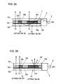
- Figs. 3A and 3B are figures for explanation of the functioning of the liquid crystal display panel 7, and they show schematic cross sections of the liquid crystal panel 7.
- Fig. 3A shows a first display state in which only the AF area marks 72 are being displayed
- Fig. 3B shows a second display state in which only the crop region 73 is being displayed.
- This liquid crystal display panel 7 is a diffraction optical element that utilizes a polymer-dispersed liquid crystal.
- a liquid crystal layer 702 that is sandwiched between transparent substrates 700 and 701
- an object hologram 704 that corresponds to the crop region 73.
- electrodes 705, 706, and 707 are formed from transparent electrically conductive layers made from ITO (tin doped indium oxide) or the like.
- the electrodes 706 and 707 are formed in the same shapes as the AF area marks 72 and the crop region 73 respectively, while the electrode 705 is formed as a background pattern over the entire substrate surface. It should be understood that, although peripheral electrodes other than the electrodes 706 and 707 are formed upon the side of the transparent substrate 701, these are not shown in the drawings.
- the polymer-dispersed liquid crystal is a substance in which a liquid crystal is dispersed within a polymer as liquid crystal droplets.
- a diffraction grating is formed by interference pattern in which polymer layers and layers in which these liquid crystal droplets are distributed in large numbers are alternatingly repeated.
- the liquid crystal molecules are oriented randomly, so that the diffraction function of the Bragg diffraction grating 703 is manifested due to the refractive index difference between the polymer layers and the liquid crystal droplet layers.
- the illumination light L that is incident into the liquid crystal panel 7 via the light guiding element 9 is diffracted by the Bragg diffraction grating 703 in the direction of the eyepiece lens 6 (refer to Fig. 1).
- the Bragg diffraction grating 703 is patterned in the shape of the AF area mark, and the observer is able to see that the portion of the AF area mark 72 is emitting light, since only this portion emits the illumination light in the direction of his line of sight.
- the applied voltage to the electrode 706 is turned ON, then the liquid crystal molecules of the liquid crystal droplet layer are oriented in the direction perpendicular to the substrate, so that the liquid crystal droplet layer comes to have almost the same refractive index as the polymer layer.
- the diffraction function of the Bragg diffraction grating 703 is eliminated, and the AF area mark 72 is not observed, since the illumination light L is not diffracted (refer to Fig. 3B).
- the Bragg diffraction grating 703 also becomes a transparent state with respect to the light LS from the photographic subject as well, so that the observer is still able to observe the image of the photographic subject formed on the viewfinder screen 4.
- a hologram of a scattering plate is formed by the liquid crystal droplets that are dispersed within a polymer.
- the diffraction function of this object hologram 704 is manifested, and the same wave front is generated for the light that is incident from underneath (i.e. the light LS from the photographic subject), as that of the scattering plate that was the model for this hologram (refer to Fig. 3B).
- the object hologram 704 operates as a scattering plate for the incident light.
- the scattered light that is emitted from this object hologram 704 is, ideally, spread out over a solid angle in all directions, so that a portion thereof comes to be observed via the penta-prism 5 and the eyepiece lens 6. As a result, the image of the photographic subject in the crop region 73 comes to be observed more darkly, as compared to the other regions.
- the diffraction function of the obj ect hologram 704 is in the ON state (i.e., the applied voltage is OFF)
- the illumination light L from the light source 8 is also scattered, accordingly the crop region 73 is undesirably observed as being luminous, so that the primary function of the crop region 73 comes to be lost. Due to this, in the second display state shown in Fig. 3B in which only the crop region 73 is displayed, the light source 8 is turned OFF in order to eliminate scattering of the illumination light in the crop region 73.
- the two types of diffraction grating 703 and 704 are disposed upon in a single liquid crystal panel 7, when the AF area mark 72 is made to emit light and to be displayed, the illumination light is scattered by the crop region 73, which is undesirable. Due to this, in this embodiment, it is arranged to employ a display method in which the display time period is time divided, and display is performed in the first display state during a portion of the time, while display is performed in the second display state during the remaining time.
- this type of time division display control is performed, the AF area mark 72 and the crop region 73 are observed as being displayed simultaneously due to an afterimage effect, since the display state of Fig. 3A and the display state of Fig. 3B are repeated alternatingly at extremely short time intervals.
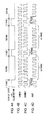
- Figs. 4A through 4D are figures showing an example of this time division display control, and show the timing signals that are outputted from the timing generator 102 of Fig. 1.
- Fig. 4A shows the signal that commands the timing for turning on/off the light source 8, and is inputted to the illumination control unit 100.
- Figs. 4B through 4D show the signals to the electrodes 705, 706, and 707, each of which is inputted to the display control unit 101.
- Fig. 4B shows a common signal related to the voltage that is applied to the common electrode 705 for the diffraction gratings 703 and 704.
- Fig. 4C shows a segment signal related to the voltage that is applied to the electrode 706, while Fig. 4D shows a crop signal related to the voltage that is applied to the electrode 707.
- a liquid crystal is driven by the method of applying a rectangular wave voltage to two electrodes on opposite sides thereof.
- the state in which the voltage applied to the electrode 707 is ON may mean the state in which the phases of the rectangular waves upon the electrode 707 and the electrode 705 differ by n
- the state in which the applied voltage is OFF may mean the state in which the phases of the rectangular waves upon the electrode 707 and the electrode 705 are the same.
- the turning ON and OFF of the applied voltage is expressed as a phase shift of the segment signal and the crop signal of Figs. 4C and 4D with respect to the common signal of Fig. 4B.
- a rectangular wave voltage of a fixed frequency is applied to the common electrode 705 by the common signal.
- ON/OFF control of the diffraction gratings 72 and 73 is performed by changing the phases of the segment signal and the crop signal.
- lighting up of the light source 8 is synchronized with the ON state of the diffraction grating 703, while turning off of the light source 8 is synchronized with the ON state of the object hologram 704. Due to this, changing over of the lighting up signal of Fig.
- the segment signal is generated so as to have the same phase as the common signal, while the crop signal is generated so as to be phase shifted by n with respect to the common signal.
- the object hologram 704 is put into the OFF state, and in this time period only the AF area mark 72 comes to be displayed. In this time period, since the object hologram 704 comes to be in the transparent state both with respect to the light from the photographic subject and also with respect to the illumination light, accordingly the crop region 73 is neither brightened nor dimmed.
- the crop signal is generated so as to have the same phase as the common signal, while the segment signal is generated so as to be phase shifted by n with respect to the common signal.
- the diffraction grating 703 is put into the OFF state, and in this time period only the crop region 73 is displayed as dimmed. In this time period, since the light source 8 is turned OFF, accordingly the crop region 73 is not caused to shine by the illumination light.
- the ratio between the time interval for the first display state and the time interval for the second display state is made to be 1:4
- the light emission luminance of the AF area mark 72 is made to be 10
- the light emission intensity when blended display is performed becomes 1/5
- the dimming of the crop region 73 becomes 0.28 (in other words, the light shielding amount becomes 0.72).
- the dimmed display of the crop region 73 and the light emitting display of the AF area mark 72 are mutually compatible. It should be understood that, by changing the ratio of the time intervals, it is possible to adjust the degree of dimming of the crop region 73 and the light emission intensity of the AF area mark 72.
- the display device of this embodiment by performing time division display control as described above, it is possible to display simultaneously, with a single liquid crystal displaypanel, both a frame display in which an image such as that of the crop region 73 is darkened, and also a light emitting display such as that of the AF area mark 72.
- the AF area mark 72 is displayed as emitting light, it is desirable from the point of view of performing recognition that, when the background image of the photographic subject is dark, then it should be displayed as emitting light darkly; and, conversely, if the image of the photographic subject is bright, then it is desirable for it to be displayed as emitting light brightly.
- the light source 8 since control for changing the electrical current for the LED that is being used as the light source 8 is difficult, in the time interval for the first display state, the light source 8 is not caused to emit light at a fixed intensity, but rather control is performed to time divide the section up more finely so as to turn the light source 8 ON and OFF repeatedly.
- Figs. 5A and 5B are figures for explanation of this time division control for illumination.
- the light emission control shown by the thick line shows the case in which light is emitted continuously
- the light emitting control shown by the thin line shows time division control.
- the horizontal axis is time
- the vertical axis is the electrical current to the light source 8.
- the time period t is the time interval shown in Figs. 4A through 4D for the first display state, while I is the rated electrical current value for the LED.
- the duty ratio for the illumination time period is 1/8, so that, by causing a current flow of 8I that is eight times the rated current value, it is arranged to obtain a light emission intensity that is equal to the intensity of continuous light emission at the rated current I. Furthermore, as shown in Fig. 5B, by setting the current value to 81, and by making the duty ratio of the illumination period during time division light emission to be 1/5, it becomes possible to obtain a light emission intensity equal to that of continuous light emission at an electrical current value of 8I/5.
- Fig. 6 is a flow chart showing a manufacturing method for a liquid crystal display panel 7 (i.e., a display element), according to an embodiment of the present invention.
- the Bragg diffraction grating is formed within the display substrate 7; in more detail, in a first region of the liquid crystal layer 702.
- the object hologram 704 is formed within the display substrate 7; in more detail, in a second region within the liquid crystal layer 702 that is different from the first region.
- Fig. 7 is a flow chart showing a manufacturing method for a display device, according to an embodiment of the present invention.
- the display substrate 7 is provided that includes the liquid crystal layer 702.
- a plurality of diffraction gratings having different diffraction modes are provided to the display substrate 7; in more detail, in regions in the liquid crystal layer 702 that are mutually different from one another.
- this plurality of diffraction gratings that have different diffraction modes may be, for example, the Bragg diffraction grating 703 and the object hologram 704.
- a controller 10 is provided that alternately controls this plurality of diffraction gratings to diffraction states.
- Fig. 8 is a flow chart for explanation of a display method that utilizes a display device according to an embodiment of the present invention. This processing is performed by the control device 10.
- a step S21 along with setting the Bragg diffraction grating 703 that is formed in the liquid crystal layer 702 of the liquid crystal display panel 7 to the diffraction state, the object hologram 704 that is formed in the liquid crystal layer 702 is set to the non-diffraction state. Furthermore, the light beam from the light source 8 is irradiated into the liquid crystal panel 7 so as to achieve the first display state (refer to Fig. 3A).
- step S22 along with not irradiating any light beam into the liquid crystal display panel 7 and setting the object hologram 704 to the diffraction state, the Bragg diffraction grating 703 is set to the non-diffracting state, so as to achieve the second display state (refer to Fig. 3B) .
- step S23 control is performed so as to repeat the first display state and the second display state alternatingly.
- the present invention could also be applied to a camera that utilizes a silver halide film as the image capture element 2. It should be understood that, although two types of diffraction gratings having different diffraction modes were provided to the liquid crystal display panel 7, it would also be acceptable to provide three or more types of diffraction gratings. Furthermore, the present invention is not to be considered as being limited in any way by the embodiments described above, provided that its characterizing features are not lost.
Landscapes
- Physics & Mathematics (AREA)
- Nonlinear Science (AREA)
- General Physics & Mathematics (AREA)
- Chemical & Material Sciences (AREA)
- Mathematical Physics (AREA)
- Crystallography & Structural Chemistry (AREA)
- Optics & Photonics (AREA)
- Dispersion Chemistry (AREA)
- Liquid Crystal (AREA)
- Control Of Indicators Other Than Cathode Ray Tubes (AREA)
- Diffracting Gratings Or Hologram Optical Elements (AREA)
- Liquid Crystal Display Device Control (AREA)
Abstract
Description
- The present invention relates to a display element that utilizes a liquid crystal, to a display device that is equipped with such a display element, and to a camera.
- From the prior art, there is known an in-viewfinder display device that utilizes a liquid crystal panel such as the one described in
Japanese Laid-Open Patent Publication 2004-191415 - However in order to use a combination of different diffraction modes in this display device such as a liquid crystal diffraction grating panel anda liquid crystal hologram, the size of the display device comes to be undesirably increased.
- A display element that holds a layer of liquid crystal between substrates according to a 1st aspect of the present invention includes a plurality of diffraction gratings having different diffraction modes, arranged in regions of the substrates that are different from one another.
- According to a 2nd aspect of the present invention, in the display element according to the 1st aspect, the plurality of diffraction gratings may include a first diffraction grating disposed in a first region of the substrates; and a second diffraction grating that is disposed in a second region peripheral to the first region, and has a diffraction mode that is different from a diffraction mode of the first diffraction grating.
- According to a 3rd aspect of the present invention, in the display element according to the 1st or 2nd aspect, each of the plurality of diffraction gratings may create a different diffraction state with respect to the liquid crystal.
- According to a 4th aspect of the present invention, in the display element according to any one of the 1st through 3rd aspect, the plurality of diffraction gratings may have a Bragg diffraction grating that diffracts an illumination light beam in a predetermined direction, and a hologram that creates scattered light.
- A display device that includes a display substrate comprising a liquid crystal according to a 5th aspect of the present invention includes a pluralityofdiffraction gratings having different diffraction modes, arranged in regions of the display substrate that are different from one another; and a controller that controls the plurality of diffraction gratings alternatingly to their diffraction states.
- According to a 6th aspect of the present invention, the display device according to the 5th aspect may further include a light source that irradiates an illumination light beam upon the display substrate, and it is preferable that the plurality of diffraction gratings comprise a Bragg diffraction grating that diffracts an incident light beam in a predetermined direction, and a hologram that creates scattered light; and the controller performs control so as to alternatingly repeat a first display state in which the illumination light beam is irradiated, the diffraction state of the Bragg diffraction grating is implemented, and moreover the diffraction state of the hologram is canceled, and a second display state in which the illumination light beam is not irradiated, the diffraction state of the Bragg diffraction grating is eliminated, and moreover the diffraction state of the hologram is implemented.
- According to a 7th aspect of the present invention, in the display device according to the 6th aspect, the light source may be a light emitting diode; and the controller may determine an effective amount of light generated by the light emitting diode, based upon a ratio between a continuous time period of the first display state, and a continuous time period of the second display state.
- According to a 8th aspect of the present invention, in the display device according to the 7th aspect, it is preferable that the controller controls an amount of light generated by the light emitting diode to the effective amount of light generated, by alternatingly repeating, within the continuous time period of the first display state, lighting up the light emitting diode with an electrical current that is greater than its static rated electrical current, and turning off the light emitting diode.
- A camera according to a 9th aspect of the present invention includes a display device that comprises a plurality of diffraction gratings having different diffraction modes, arranged in regions of a display substrate comprising a liquid crystal that are different from one another; and a controller that controls the plurality of diffraction gratings alternatingly to their diffraction states.
- According to a 10th aspect of the present invention, the camera according to the 9th aspect may further include a light source that irradiates an illumination light beam upon the display substrate, and it is preferable that the plurality of diffraction gratings comprise a Bragg diffraction grating that diffracts an incident light beam in a predetermined direction, and a hologram that creates scattered light; and the controller performs control so as to alternatingly repeat a first display state in which the illumination light beam is irradiated, the diffraction state of the Bragg diffraction grating is implemented, and moreover the diffraction state of the hologram is canceled, and a second display state in which the illumination light beam is not irradiated, the diffraction state of the Bragg diffraction grating is eliminated, and moreover the diffraction state of the hologram is implemented.
- According to a 11th aspect of the present invention, in the camera according to the 10th aspect, the controller may perform display of photographic information by putting the Bragg diffraction grating into its diffraction state, and changes a region of the display substrate through which light passes by putting the hologram into its diffraction state.
- A method for manufacturing a display element that comprises diffraction gratings according to a 12th aspect of the present invention: forms a first diffraction grating in a first region in a display substrate; and forms a second diffraction grating whose diffraction mode differs from a diffraction mode of the first diffraction grating, in a second region in the display substrate that is different from the first region.
- According to a 13th aspect of the present invention, in the method for manufacturing a display element according to the 12th aspect: a Bragg diffraction grating that diffracts an illumination light beam in a predetermined direction may be used as the first diffraction grating, and a hologram that creates scattered light may be used as the second diffraction grating.
- A method for manufacturing a display device that comprises diffraction gratings according to a 14th aspect of the present invention: provides a display substrate that comprises a liquid crystal; provides, in mutually different regions of the display substrate, a plurality of diffraction gratings each of which has a different diffraction mode; and provides a controller that controls the diffraction states of the plurality of diffraction gratings alternatingly.
- According to a 15th aspect of the present invention, in the method for manufacturing a display device according to the 14th aspect: the plurality of diffraction gratings may include a Bragg diffraction grating that diffracts an illumination light beam in a predetermined direction, and a hologram that creates scattered light.
- A display method for a display device that comprises diffraction gratings according to a 16th aspect of the present invention: establishes a first display state in which, along with putting a Bragg diffraction grating that is provided in a first region of a display substrate that comprises a liquid crystal into its diffraction state, a hologram that is provided in a second region of the display substrate that is different from the first region is put into its non-diffraction state, and a light beam is irradiated from a light source upon the display substrate; establishes a second display state in which, along with not irradiating the light beam upon the display substrate and putting the hologram into its diffraction state, the Bragg diffraction grating is put into its non-diffraction state; and alternatingly repeates the first display state and the second display state.
- According to a 17th aspect of the present invention, in the display method according to the 16th aspect, the irradiation of the light beam may be performed with an amount of generated light that is determined based upon a ratio between a continuous time period of the first display state and a continuous time period of the second display state.
- According to a 18th aspect of the present invention, in the display method according to the 17th aspect, the amount of generated light may be controlled, within the continuous time period of the first display state, by repeating lighting up the light source with an electrical current that is greater than its static rated electrical current, and turning off the light source.
- According to a 19th aspect of the present invention, in the display method according to the 16th aspect, along with performing display of information in the first display state, a region of the display substrate through which light passes may be changed in the second display state.
-
- Fig. 1 is a figure showing an embodiment of a display device according to the present invention;
- Fig. 2 is a plan view of a liquid crystal display panel;
- Figs. 3A and 3B are schematic figures for explanation of the functioning of this liquid crystal display panel: Fig. 3A shows a first display state thereof, while Fig. 3B shows a second display state thereof;
- Figs. 4A through 4D are figures showing an example of time division display control: Fig. 4A shows a signal that commands the timing for illuminating a light source, Fig. 4B shows a common signal, Fig. 4C shows a segment signal, and Fig. 4D shows a crop signal;
- Figs. 5A and 5B are figures for explanation of this time division control for illumination: Fig. 5A shows a case in which the duty ratio of the illuminated time period is 1/8, while Fig. 5B shows a case in which the duty ratio of the illuminated time period is 1/5;
- Fig. 6 is a flow chart showing a manufacturing method for a display element according to an embodiment;
- Fig. 7 is a flow chart showing a manufacturing method for a display device according to an embodiment; and
- Fig. 8 is a flow chart for explanation of a displaymethod that utilizes a display device according to an embodiment.
- In the following, preferred embodiments for implementation of the present invention will be explained with reference to the figures. Fig. 1 is a figure showing an embodiment of a display device according to the present invention, and is a general structural figure for a case in which this display device is applied as a viewfinder display device of a camera. The reference symbol 1 denotes a photographic lens. An image of a light flux from a photographic subject is formed upon an
image sensor 2 by this photographic lens 1, and an image of the photographic subject having been formed is captured by theimage sensor 2. A solid-state image capture element such as a CCD or a CMOS or the like may be employed as thisimage sensor 2. - Between the photographic lens 1 and the
image sensor 2, there is provided amirror 3 that reflects the light flux from the photographic subject towards a viewfinder optical system. During exposure, thismirror 3 is driven so as to be shunted away from the optical path, so that the image of the photographic subject is projected upon theimage sensor 2. On the other hand, when exposure is not being performed, the light flux from the photographic subject having passed through the photographic lens 1 is reflected by themirror 3, and is imaged upon a viewfinder screen 4 that is disposed in a position that is optically equivalent to the image capturing surface of theimage sensor 2. This image of the photographic subject that has been formed upon the viewfinder screen 4 maybe observed via a penta-prism 5 and aneyepiece lens 6. - A liquid
crystal display panel 7 for performing in-viewfinder display is provided above and in the neighborhood of the viewfinder screen 4. And, at the side of this liquidcrystal display panel 7, there is disposed alight source 8 that illuminates the liquidcrystal display panel 7. In this embodiment, a light emitting diode (LED) is used as thelight source 8. The illumination light that has been emitted from thislight source 8 is incident upon the liquidcrystal display panel 7 via alight guiding element 9. Thislight guiding element 9 is an optical element for conducting the illumination light into the liquidcrystal display panel 7 with good efficiency. The display light from the liquidcrystal display panel 7 arrives at theeyepiece lens 6 via the penta-prism 5. As a result, a display is superimposed upon the image of the photographic subj ect, and the image of the photographic subject with the display superimposed may be observed. - The
reference symbol 10 denotes a control device for controlling a display to be superimposed upon the image of the photographic subject. Thiscontrol device 10 includes anillumination control unit 100 that controls the drive of thelight source 8, adisplay control unit 101 that controls the drive of the liquidcrystal display panel 7, and atiming generator 102 that outputs a signal for the ON/OFF timing of this illumination and display. Theillumination control unit 100 and thedisplay control unit 101 perform their respective control actions, based upon the timing signals that are inputted from thetiming generator 102. - Fig. 2 is a plan view of the liquid
crystal display panel 7. A plurality ofAF area marks 72 are arranged in the center of the screen, and it is possible to display any one of these selectively, so as to show the position of a subject upon which focal point adjustment is to be performed. Furthermore, this camera is provided with a function of selecting an image capture region from a plurality of image capture regions, and it is arranged that the selected image capture regions can be recognized in a simple manner, by displaying a field of view frame for the photographic subject with crop regions 73 (73a, 73b, and 73c) upon which hatching is provided. When none of thesecrop regions 73a through 73c is displayed, then therectangular region 71 that has dimensions E vertically by D horizontally shows the normal (maximum) image capture area, while it is arranged for it to be possible to display smaller image capture regions by displaying thecrop regions 73a through 73c. - When the left and right pair of
crop regions 73c are displayed, the image capture region becomes E vertically by C horizontally. When the left and right pairs ofcrop regions crop regions 73a through 73c are displayed, the image capture region becomes F vertically by A horizontally. Since image processing and so on are performed based upon image capture signals, in the image capture signal outputted from theimage sensor 2, from image capture regions that correspond to these image capture regions, accordingly, the smaller the image capture region becomes, the smaller does the image size become, as is appropriate for high speed photography. - Figs. 3A and 3B are figures for explanation of the functioning of the liquid
crystal display panel 7, and they show schematic cross sections of theliquid crystal panel 7. Fig. 3A shows a first display state in which only the AF area marks 72 are being displayed, while Fig. 3B shows a second display state in which only thecrop region 73 is being displayed. This liquidcrystal display panel 7 is a diffraction optical element that utilizes a polymer-dispersed liquid crystal. In aliquid crystal layer 702 that is sandwiched betweentransparent substrates Bragg diffraction grating 703 that corresponds to the AF area marks 72, and anobject hologram 704 that corresponds to thecrop region 73. - Upon the surfaces of the
transparent substrates liquid crystal layer 702,electrodes electrodes crop region 73 respectively, while theelectrode 705 is formed as a background pattern over the entire substrate surface. It should be understood that, although peripheral electrodes other than theelectrodes transparent substrate 701, these are not shown in the drawings. - The polymer-dispersed liquid crystal is a substance in which a liquid crystal is dispersed within a polymer as liquid crystal droplets. In the
Bragg diffraction grating 703, a diffraction grating is formed by interference pattern in which polymer layers and layers in which these liquid crystal droplets are distributed in large numbers are alternatingly repeated. In the state in which the applied voltage to theelectrode 706 is turned OFF so that no electrical potential difference is present between theelectrodes Bragg diffraction grating 703 is manifested due to the refractive index difference between the polymer layers and the liquid crystal droplet layers. - As shown in Fig. 3A, when the
light source 8 is turned ON and the applied voltage to theelectrode 706 is turned OFF, then the illumination light L that is incident into theliquid crystal panel 7 via thelight guiding element 9 is diffracted by theBragg diffraction grating 703 in the direction of the eyepiece lens 6 (refer to Fig. 1). TheBragg diffraction grating 703 is patterned in the shape of the AF area mark, and the observer is able to see that the portion of theAF area mark 72 is emitting light, since only this portion emits the illumination light in the direction of his line of sight. It should be understood that, since a voltage is always applied to a peripheral electrode not shown in the figure, accordingly the liquid crystal molecules are oriented in the direction perpendicular to the substrate, and theliquid crystal layer 702 is put into a transparent state, so that the light LS from the photographic subject passes through thisliquid crystal layer 702. Due to this, the observer is able to observe an image of the photographic subject upon the viewfinder screen 4. - On the other hand, when the applied voltage to the
electrode 706 is turned ON, then the liquid crystal molecules of the liquid crystal droplet layer are oriented in the direction perpendicular to the substrate, so that the liquid crystal droplet layer comes to have almost the same refractive index as the polymer layer. As a result, the diffraction function of theBragg diffraction grating 703 is eliminated, and theAF area mark 72 is not observed, since the illumination light L is not diffracted (refer to Fig. 3B). Furthermore, theBragg diffraction grating 703 also becomes a transparent state with respect to the light LS from the photographic subject as well, so that the observer is still able to observe the image of the photographic subject formed on the viewfinder screen 4. - In the
object hologram 704 that is formed in thecrop region 73, a hologram of a scattering plate is formed by the liquid crystal droplets that are dispersed within a polymer. In the state in which no voltage is applied to theelectrode 707, the diffraction function of thisobject hologram 704 is manifested, and the same wave front is generated for the light that is incident from underneath (i.e. the light LS from the photographic subject), as that of the scattering plate that was the model for this hologram (refer to Fig. 3B). In other words, theobject hologram 704 operates as a scattering plate for the incident light. The scattered light that is emitted from thisobject hologram 704 is, ideally, spread out over a solid angle in all directions, so that a portion thereof comes to be observed via the penta-prism 5 and theeyepiece lens 6. As a result, the image of the photographic subject in thecrop region 73 comes to be observed more darkly, as compared to the other regions. - On the other hand, when the voltage applied to the
electrode 707 is turned ON, then the diffraction function of theobject hologram 704 is eliminated, since the liquid crystal molecules in the liquid crystal droplet layer are oriented in the direction perpendicular to the substrate. As a result, the light LS from the photographic subject is not scattered by thecrop region 73, and passes through the liquid crystal panel 7 (refer to Fig. 3A). - Now, when the diffraction function of the
obj ect hologram 704 is in the ON state (i.e., the applied voltage is OFF), since the illumination light L from thelight source 8 is also scattered, accordingly thecrop region 73 is undesirably observed as being luminous, so that the primary function of thecrop region 73 comes to be lost. Due to this, in the second display state shown in Fig. 3B in which only thecrop region 73 is displayed, thelight source 8 is turned OFF in order to eliminate scattering of the illumination light in thecrop region 73. - In other words, if the two types of
diffraction grating liquid crystal panel 7, when theAF area mark 72 is made to emit light and to be displayed, the illumination light is scattered by thecrop region 73, which is undesirable. Due to this, in this embodiment, it is arranged to employ a display method in which the display time period is time divided, and display is performed in the first display state during a portion of the time, while display is performed in the second display state during the remaining time. When this type of time division display control is performed, theAF area mark 72 and thecrop region 73 are observed as being displayed simultaneously due to an afterimage effect, since the display state of Fig. 3A and the display state of Fig. 3B are repeated alternatingly at extremely short time intervals. - Figs. 4A through 4D are figures showing an example of this time division display control, and show the timing signals that are outputted from the
timing generator 102 of Fig. 1. Fig. 4A shows the signal that commands the timing for turning on/off thelight source 8, and is inputted to theillumination control unit 100. And Figs. 4B through 4D show the signals to theelectrodes display control unit 101. Fig. 4B shows a common signal related to the voltage that is applied to thecommon electrode 705 for thediffraction gratings electrode 706, while Fig. 4D shows a crop signal related to the voltage that is applied to theelectrode 707. - Generally, a liquid crystal is driven by the method of applying a rectangular wave voltage to two electrodes on opposite sides thereof. For example, the state in which the voltage applied to the
electrode 707 is ON may mean the state in which the phases of the rectangular waves upon theelectrode 707 and theelectrode 705 differ by n, while the state in which the applied voltage is OFF may mean the state in which the phases of the rectangular waves upon theelectrode 707 and theelectrode 705 are the same. In other words, the turning ON and OFF of the applied voltage is expressed as a phase shift of the segment signal and the crop signal of Figs. 4C and 4D with respect to the common signal of Fig. 4B. - A rectangular wave voltage of a fixed frequency is applied to the
common electrode 705 by the common signal. And ON/OFF control of thediffraction gratings light source 8 is synchronized with the ON state of thediffraction grating 703, while turning off of thelight source 8 is synchronized with the ON state of theobject hologram 704. Due to this, changing over of the lighting up signal of Fig. 4A between the HI state and the LO state is synchronized with the changing over between the first display state in which only theAF area mark 72 is displayed, and the second display state in which only thecrop region 73 is displayed, respectively shown in Figs. 3A and 3B. - In the first display state in which the lighting up signal for the
light source 8 is in the HI state, the segment signal is generated so as to have the same phase as the common signal, while the crop signal is generated so as to be phase shifted by n with respect to the common signal. As a result, along with thediffraction grating 703 being put into the ON state, also theobject hologram 704 is put into the OFF state, and in this time period only theAF area mark 72 comes to be displayed. In this time period, since theobject hologram 704 comes to be in the transparent state both with respect to the light from the photographic subject and also with respect to the illumination light, accordingly thecrop region 73 is neither brightened nor dimmed. - On the other hand, in the second display state in which the lighting up signal for the
light source 8 is in the LO state, the crop signal is generated so as to have the same phase as the common signal, while the segment signal is generated so as to be phase shifted by n with respect to the common signal. As a result, along with theobject hologram 704 being put into the ON state, also thediffraction grating 703 is put into the OFF state, and in this time period only thecrop region 73 is displayed as dimmed. In this time period, since thelight source 8 is turned OFF, accordingly thecrop region 73 is not caused to shine by the illumination light. - Since the change over between the first and second display states is repeated at a shorter time interval than that at which a human being can discriminate temporal decomposition, accordingly the observer comes to see that the first display state and the second display state are blended together, due to the afterimage effect. Here, if the ratio between the time interval for the first display state and the time interval for the second display state is made to be 1:4, the light emission luminance of the
AF area mark 72 is made to be 10, and the dimming ratio of the crop region 73 (= 1 - the amount of light shielding) is made to be 0.1, then the light emission intensity when blended display is performed becomes 1/5, while the dimming of thecrop region 73 becomes 0.28 (in other words, the light shielding amount becomes 0.72). Due to this, it will be understood that the dimmed display of thecrop region 73 and the light emitting display of theAF area mark 72 are mutually compatible. It should be understood that, by changing the ratio of the time intervals, it is possible to adjust the degree of dimming of thecrop region 73 and the light emission intensity of theAF area mark 72. - In this manner, with the display device of this embodiment, by performing time division display control as described above, it is possible to display simultaneously, with a single liquid crystal displaypanel, both a frame display in which an image such as that of the
crop region 73 is darkened, and also a light emitting display such as that of theAF area mark 72. - Now, if the
AF area mark 72 is displayed as emitting light, it is desirable from the point of view of performing recognition that, when the background image of the photographic subject is dark, then it should be displayed as emitting light darkly; and, conversely, if the image of the photographic subject is bright, then it is desirable for it to be displayed as emitting light brightly. In this case, since control for changing the electrical current for the LED that is being used as thelight source 8 is difficult, in the time interval for the first display state, thelight source 8 is not caused to emit light at a fixed intensity, but rather control is performed to time divide the section up more finely so as to turn thelight source 8 ON and OFF repeatedly. - Figs. 5A and 5B are figures for explanation of this time division control for illumination. In Fig. 5A, the light emission control shown by the thick line shows the case in which light is emitted continuously, while the light emitting control shown by the thin line shows time division control. It should be understood that the horizontal axis is time, while the vertical axis is the electrical current to the
light source 8. The time period t is the time interval shown in Figs. 4A through 4D for the first display state, while I is the rated electrical current value for the LED. - In the case of an LED, generation of heat is the reason why a large electrical current is not caused to flow continuously. It is possible to flow a much larger electrical current for a short time period. In the example shown in Fig. 5A, the duty ratio for the illumination time period is 1/8, so that, by causing a current flow of 8I that is eight times the rated current value, it is arranged to obtain a light emission intensity that is equal to the intensity of continuous light emission at the rated current I. Furthermore, as shown in Fig. 5B, by setting the current value to 81, and by making the duty ratio of the illumination period during time division light emission to be 1/5, it becomes possible to obtain a light emission intensity equal to that of continuous light emission at an electrical current value of 8I/5.
- Fig. 6 is a flow chart showing a manufacturing method for a liquid crystal display panel 7 (i.e., a display element), according to an embodiment of the present invention.
- In a step S1, the Bragg diffraction grating is formed within the
display substrate 7; in more detail, in a first region of theliquid crystal layer 702. And in a step S2, theobject hologram 704 is formed within thedisplay substrate 7; in more detail, in a second region within theliquid crystal layer 702 that is different from the first region. - Fig. 7 is a flow chart showing a manufacturing method for a display device, according to an embodiment of the present invention.
- In a step S11, the
display substrate 7 is provided that includes theliquid crystal layer 702. And in a step S12, a plurality of diffraction gratings having different diffraction modes are provided to thedisplay substrate 7; in more detail, in regions in theliquid crystal layer 702 that are mutually different from one another. Here, this plurality of diffraction gratings that have different diffraction modes may be, for example, theBragg diffraction grating 703 and theobject hologram 704. And, in a step S13, acontroller 10 is provided that alternately controls this plurality of diffraction gratings to diffraction states. - Fig. 8 is a flow chart for explanation of a display method that utilizes a display device according to an embodiment of the present invention. This processing is performed by the
control device 10. - In a step S21, along with setting the
Bragg diffraction grating 703 that is formed in theliquid crystal layer 702 of the liquidcrystal display panel 7 to the diffraction state, theobject hologram 704 that is formed in theliquid crystal layer 702 is set to the non-diffraction state. Furthermore, the light beam from thelight source 8 is irradiated into theliquid crystal panel 7 so as to achieve the first display state (refer to Fig. 3A). - And, in a step S22, along with not irradiating any light beam into the liquid
crystal display panel 7 and setting theobject hologram 704 to the diffraction state, theBragg diffraction grating 703 is set to the non-diffracting state, so as to achieve the second display state (refer to Fig. 3B) . Then, in a step S23, control is performed so as to repeat the first display state and the second display state alternatingly. - A summary of the advantageous operational effects of the embodiments explained above is as follows.
- (1) Since each of the plurality of
diffraction gratings liquid crystal layer 702, and in different regions thereof, accordingly it is possible to perform display of different diffraction modes with a single liquid crystal panel, and it is possible to make the display device more compact. It should be understood that it would also be acceptable, as the diffraction gratings of different diffraction modes, to provide a Bragg diffraction grating that diffracts the illumination light beam in a predetermined direction, and a hologram that emits scattered light. - (2) The display device according to the embodiment includes the
display element 7, theillumination device 8 that illuminates thedisplay element 7, and thecontrol device 10 that controls the implementation of the diffraction states and theillumination device 8. Thiscontrol device 10 performs time division display control by alternatingly repeating the first display state in which theillumination device 8 is turned on, theBragg diffraction grating 703 is set to the diffraction state, and the diffraction state of thehologram 704 is cancelled, and the second display state in which, along with canceling theillumination device 8 and the diffraction state of theBragg diffraction grating 703, the diffraction state of thehologram 704 is implemented. As a result, along with it being possible to anticipate making the display device more compact, also it is possible to perform display according to the different diffraction modes that are provided upon the same substrate simultaneously. It should be understood that it would also be acceptable to arrange to use a light emitting diode as theillumination device 8, and to determine the effective amount of light generated by the light emitting diode, based upon the ratio between the continuous time period in the first display state, and the continuous time period in the second display state. - (3) By alternatingly repeating, within the time interval that the first display state continues, lighting up and turning off of the light emitting diode at an electrical current that exceeds its static rated electric current so as to control the amount of light generated by the light emitting diode to an effective amount of generated light, along with it being possible to perform control of the effective amount of generated light in a simple manner, it is also possible to change it dynamically.
- Although in this embodiment, by way of example, a digital camera was explained that used a solid image capture element such as a CCD or a CMOS for the image capture element, the present invention could also be applied to a camera that utilizes a silver halide film as the
image capture element 2. It should be understood that, although two types of diffraction gratings having different diffraction modes were provided to the liquidcrystal display panel 7, it would also be acceptable to provide three or more types of diffraction gratings. Furthermore, the present invention is not to be considered as being limited in any way by the embodiments described above, provided that its characterizing features are not lost. - The above-described embodiments are examples, and various modifications can be made without departing from the scope of the invention.
Claims (19)
- A display element that holds a layer of liquid crystal between substrates, comprising:a plurality of diffraction gratings (703, 704) having different diffraction modes, arranged in regions of the substrates that are different from one another.
- A display element according to claim 1, wherein:the plurality of diffraction gratings comprises a first diffraction grating disposed in a first region of the substrates; and a second diffraction grating that is disposed in a second region peripheral to the first region, and has a diffraction mode that is different from a diffraction mode of the first diffraction grating.
- A display element according to Claim 1 or Claim 2, wherein:each of the plurality of diffraction gratings creates a different diffraction state with respect to the liquid crystal.
- A display element according to any one of Claims 1 through 3, wherein:the plurality of diffraction gratings comprise a Bragg diffraction grating that diffracts an illumination light beam in a predetermined direction, and a hologram that creates scattered light.
- A display device that comprises a display substrate comprising a liquid crystal, comprising:a plurality of diffraction gratings (703, 704) having different diffractionmodes, arranged in regions of the display substrate that are different from one another; anda controller (10) that controls the plurality of diffraction gratings (703, 704) alternatingly to their diffraction states.
- A display device according to Claim 5, further comprising:a light source that irradiates an illumination light beam upon the display substrate, and wherein:the plurality of diffraction gratings comprise a Bragg diffraction grating that diffracts an incident light beam in a predetermined direction, and a hologram that creates scattered light; andthe controller performs control so as to alternatingly repeat a first display state in which the illumination light beam is irradiated, the diffraction state of the Bragg diffraction grating is implemented, and moreover the diffraction state of the hologram is canceled, and a second display state in which the illumination light beam is not irradiated, the diffraction state of the Bragg diffraction grating is eliminated, and moreover the diffraction state of the hologram is implemented.
- A display device according to Claim 6, wherein:the light source is a light emitting diode; andthe controller determines an effective amount of light generated by the light emitting diode, based upon a ratio between a continuous time period of the first display state, and a continuous time period of the second display state.
- A display device according to Claim 7, wherein:the controller controls an amount of light generated by the light emitting diode to the effective amount of light generated, by alternatingly repeating, within the continuous time period of the first display state, lighting up the light emitting diode with an electrical current that is greater than its static rated electrical current, and turning off the light emitting diode.
- A camera, comprising:a display device (7) that comprises a plurality of diffraction gratings (703, 704) having different diffraction modes, arranged in regions of a display substrate comprising a liquid crystal that are different from one another; anda controller (10) that controls the plurality of diffraction gratings (703, 704) alternatingly to their diffraction states.
- A camera according to Claim 9, further comprising:a light source that irradiates an illumination light beam upon the display substrate, and wherein:the plurality of diffraction gratings comprise a Bragg diffraction grating that diffracts an incident light beam in a predetermined direction, and a hologram that creates scattered light; andthe controller performs control so as to alternatingly repeat a first display state in which the illumination light beam is irradiated, the diffraction state of the Bragg diffraction grating is implemented, and moreover the diffraction state of the hologram is canceled, and a second display state in which the illumination light beam is not irradiated, the diffraction state of the Bragg diffraction grating is eliminated, and moreover the diffraction state of the hologram is implemented.
- A camera according to Claim 10, wherein:the controller performs display of photographic information by putting the Bragg diffraction grating into its diffraction state, and changes a region of the display substrate through which light passes by putting the hologram into its diffraction state.
- A method for manufacturing a display element that comprises diffraction gratings, comprising:forming a first diffraction grating in a first region in a display substrate; andforming a second diffraction grating whose diffraction mode differs from a diffraction mode of the first diffraction grating, in a second region in the display substrate that is different from the first region.
- A method for manufacturing a display element according to Claim 12, wherein:a Bragg diffraction grating that diffracts an illumination light beam in a predetermined direction is used as the first diffraction grating, and a hologram that creates scattered light is used as the second diffraction grating.
- A method for manufacturing a display device that comprises diffraction gratings, comprising:providing a display substrate that comprises a liquid crystal;providing, in mutually different regions of the display substrate, a plurality of diffraction gratings each of which has a different diffraction mode; andproviding a controller that controls the diffraction states of the plurality of diffraction gratings alternatingly.
- A method for manufacturing a display device according to Claim 14, wherein:the plurality of diffraction gratings comprise a Bragg diffraction grating that diffracts an illumination light beam in a predetermined direction, and a hologram that creates scattered light.
- A display method for a display device that comprises diffraction gratings, comprising:establishing a first display state in which, along with putting a Bragg diffraction grating that is provided in a first region of a display substrate that comprises a liquid crystal into its diffraction state, a hologram that is provided in a second region of the display substrate that is different from the first region is put into its non-diffraction state, and a light beam is irradiated from a light source upon the display substrate;establishing a second display state in which, along with not irradiating the light beam upon the display substrate and putting the hologram into its diffraction state, the Bragg diffraction grating is put into its non-diffraction state; andalternatingly repeating the first display state and the second display state.
- A display method according to Claim 16, wherein:the irradiation of the light beam is performed with an amount of generated light that is determined based upon a ratio between a continuous time period of the first display state and a continuous time period of the second display state.
- A display method according to Claim 17, wherein:the amount of generated light is controlled, within the continuous time period of the first display state, by repeating lighting up the light source with an electrical current that is greater than its static rated electrical current, and turning off the light source.
- A display method according to Claim 16, wherein:along with performing display of information in the first display state, a region of the display substrate through which light passes is changed in the second display state.
Applications Claiming Priority (1)
| Application Number | Priority Date | Filing Date | Title |
|---|---|---|---|
| JP2006185154A JP2008015125A (en) | 2006-07-05 | 2006-07-05 | Display element, display device, and camera |
Publications (1)
| Publication Number | Publication Date |
|---|---|
| EP1876490A1 true EP1876490A1 (en) | 2008-01-09 |
Family
ID=38566996
Family Applications (1)
| Application Number | Title | Priority Date | Filing Date |
|---|---|---|---|
| EP07111764A Withdrawn EP1876490A1 (en) | 2006-07-05 | 2007-07-04 | Display element, display device, and camera |
Country Status (3)
| Country | Link |
|---|---|
| US (1) | US8040316B2 (en) |
| EP (1) | EP1876490A1 (en) |
| JP (1) | JP2008015125A (en) |
Cited By (2)
| Publication number | Priority date | Publication date | Assignee | Title |
|---|---|---|---|---|
| FR2926373A1 (en) * | 2008-01-11 | 2009-07-17 | Essilor Int | TRANSPARENT COMPONENT WITH SWITCHABLE REFLECTING ELEMENTS, AND DEVICES COMPRISING SUCH A COMPONENT |
| WO2013034879A1 (en) * | 2011-09-07 | 2013-03-14 | Milan Momcilo Popovich | Method and apparatus for switching electro optical arrays |
Families Citing this family (21)
| Publication number | Priority date | Publication date | Assignee | Title |
|---|---|---|---|---|
| WO2008105395A1 (en) * | 2007-02-26 | 2008-09-04 | Nikon Corporation | Display device, finder device, and camera |
| JP2009123553A (en) * | 2007-11-15 | 2009-06-04 | Sumitomo Chemical Co Ltd | Light guide plate, surface light source device, and liquid crystal display device |
| WO2009116637A1 (en) * | 2008-03-19 | 2009-09-24 | 旭硝子株式会社 | Image display with function for transmitting light from subject to be observed |
| US8384861B2 (en) * | 2008-07-28 | 2013-02-26 | Pixel Qi Corporation | Diffractive liquid crystal display |
| CN102043502A (en) * | 2009-10-15 | 2011-05-04 | 英华达股份有限公司 | Touch display device and manufacturing method thereof |
| US8830426B2 (en) | 2010-11-17 | 2014-09-09 | Pixel Qi Corporation | Color shift reduction in transflective liquid crystal displays |
| US11068049B2 (en) | 2012-03-23 | 2021-07-20 | Microsoft Technology Licensing, Llc | Light guide display and field of view |
| US9558590B2 (en) | 2012-03-28 | 2017-01-31 | Microsoft Technology Licensing, Llc | Augmented reality light guide display |
| US10191515B2 (en) | 2012-03-28 | 2019-01-29 | Microsoft Technology Licensing, Llc | Mobile device light guide display |
| US9717981B2 (en) | 2012-04-05 | 2017-08-01 | Microsoft Technology Licensing, Llc | Augmented reality and physical games |
| US10502876B2 (en) | 2012-05-22 | 2019-12-10 | Microsoft Technology Licensing, Llc | Waveguide optics focus elements |
| JP6033036B2 (en) * | 2012-10-19 | 2016-11-30 | アルパイン株式会社 | Information display device |
| US10192358B2 (en) | 2012-12-20 | 2019-01-29 | Microsoft Technology Licensing, Llc | Auto-stereoscopic augmented reality display |
| US10678412B2 (en) | 2014-07-31 | 2020-06-09 | Microsoft Technology Licensing, Llc | Dynamic joint dividers for application windows |
| US10254942B2 (en) | 2014-07-31 | 2019-04-09 | Microsoft Technology Licensing, Llc | Adaptive sizing and positioning of application windows |
| US10018844B2 (en) | 2015-02-09 | 2018-07-10 | Microsoft Technology Licensing, Llc | Wearable image display system |
| US10317677B2 (en) | 2015-02-09 | 2019-06-11 | Microsoft Technology Licensing, Llc | Display system |
| US11086216B2 (en) | 2015-02-09 | 2021-08-10 | Microsoft Technology Licensing, Llc | Generating electronic components |
| CN106940486B (en) * | 2017-04-25 | 2022-06-24 | 京东方科技集团股份有限公司 | Display device and display method thereof |
| CN116075946A (en) * | 2020-08-18 | 2023-05-05 | 京瓷株式会社 | display device |
| CN117238253B (en) * | 2023-08-07 | 2024-04-30 | 广州文石信息科技有限公司 | Method, device, equipment and storage medium for displaying marks of ink screen |
Citations (5)
| Publication number | Priority date | Publication date | Assignee | Title |
|---|---|---|---|---|
| US5669022A (en) * | 1994-05-31 | 1997-09-16 | Canon Kabushiki Kaisha | Optical apparatus including a light modulation finder optical system |
| WO2000016135A1 (en) * | 1998-09-14 | 2000-03-23 | Digilens, Inc. | Electrically switchable holographic display |
| JP2002072333A (en) * | 2000-06-12 | 2002-03-12 | Nikon Corp | Liquid crystal display device and finder device for electronic equipment |
| JP2002122906A (en) * | 2000-10-17 | 2002-04-26 | Olympus Optical Co Ltd | Display device in viewfinder |
| US20060034603A1 (en) * | 2002-12-06 | 2006-02-16 | Nikon Corporation | Holographic optical device, camera finder indication, and camera |
Family Cites Families (9)
| Publication number | Priority date | Publication date | Assignee | Title |
|---|---|---|---|---|
| US5751452A (en) * | 1993-02-22 | 1998-05-12 | Nippon Telegraph And Telephone Corporation | Optical devices with high polymer material and method of forming the same |
| JPH06317795A (en) * | 1993-05-06 | 1994-11-15 | Fujitsu Ltd | Liquid crystal display device |
| US5825448A (en) * | 1995-05-19 | 1998-10-20 | Kent State University | Reflective optically active diffractive device |
| US7312906B2 (en) * | 1996-07-12 | 2007-12-25 | Science Applications International Corporation | Switchable polymer-dispersed liquid crystal optical elements |
| DE60045072D1 (en) * | 1999-05-24 | 2010-11-18 | Toppan Printing Co Ltd | COMPOSITE COMPOSITE BODY, INFORMATION STORAGE MEDIUM AND DEVICE FOR APPLYING IMPACT-SAFE FEATURES |
| US6538775B1 (en) * | 1999-09-16 | 2003-03-25 | Reveo, Inc. | Holographically-formed polymer dispersed liquid crystals with multiple gratings |
| US6975810B2 (en) * | 2003-03-26 | 2005-12-13 | Nikon Corporation | Focal point detection device and camera |
| CA2558035A1 (en) * | 2004-03-17 | 2005-09-22 | Sumitomo Electric Industries, Ltd. | Hologram color filter, method for fabricating the same, and color liquid crystal display comprising it |
| JP4586630B2 (en) * | 2005-05-23 | 2010-11-24 | 株式会社ニコン | Diffraction type display device and display device in viewfinder of camera |
-
2006
- 2006-07-05 JP JP2006185154A patent/JP2008015125A/en active Pending
-
2007
- 2007-06-28 US US11/819,688 patent/US8040316B2/en not_active Expired - Fee Related
- 2007-07-04 EP EP07111764A patent/EP1876490A1/en not_active Withdrawn
Patent Citations (5)
| Publication number | Priority date | Publication date | Assignee | Title |
|---|---|---|---|---|
| US5669022A (en) * | 1994-05-31 | 1997-09-16 | Canon Kabushiki Kaisha | Optical apparatus including a light modulation finder optical system |
| WO2000016135A1 (en) * | 1998-09-14 | 2000-03-23 | Digilens, Inc. | Electrically switchable holographic display |
| JP2002072333A (en) * | 2000-06-12 | 2002-03-12 | Nikon Corp | Liquid crystal display device and finder device for electronic equipment |
| JP2002122906A (en) * | 2000-10-17 | 2002-04-26 | Olympus Optical Co Ltd | Display device in viewfinder |
| US20060034603A1 (en) * | 2002-12-06 | 2006-02-16 | Nikon Corporation | Holographic optical device, camera finder indication, and camera |
Cited By (4)
| Publication number | Priority date | Publication date | Assignee | Title |
|---|---|---|---|---|
| FR2926373A1 (en) * | 2008-01-11 | 2009-07-17 | Essilor Int | TRANSPARENT COMPONENT WITH SWITCHABLE REFLECTING ELEMENTS, AND DEVICES COMPRISING SUCH A COMPONENT |
| WO2009138604A1 (en) * | 2008-01-11 | 2009-11-19 | Essilor International (Compagnie Generale D'optique) | Transparent component with switchable reflecting members, and devices including such component |
| US8502761B2 (en) | 2008-01-11 | 2013-08-06 | Essilor International | Transparent component with switchable reflecting elements, and devices including such component |
| WO2013034879A1 (en) * | 2011-09-07 | 2013-03-14 | Milan Momcilo Popovich | Method and apparatus for switching electro optical arrays |
Also Published As
| Publication number | Publication date |
|---|---|
| JP2008015125A (en) | 2008-01-24 |
| US8040316B2 (en) | 2011-10-18 |
| US20080007952A1 (en) | 2008-01-10 |
Similar Documents
| Publication | Publication Date | Title |
|---|---|---|
| US8040316B2 (en) | Display element, display device, and camera | |
| JP4348457B2 (en) | High dynamic range display, display controller, and image display method | |
| JP5817989B2 (en) | LIGHTING DEVICE, DISPLAY DEVICE, AND ELECTRONIC DEVICE | |
| CN115004678B (en) | Electronic devices | |
| CN1289433A (en) | Color display device and color display method | |
| EP1726986B1 (en) | Diffractive display device and corresponding display method | |
| JP3539251B2 (en) | Viewfinder display device and optical apparatus having the same | |
| US5603068A (en) | Display device | |
| CN1166613A (en) | Nematic liquid crystal phase spatial light modulator for enhanced display resolution | |
| JP5218061B2 (en) | Diffraction type display device, finder device and camera | |
| KR101165437B1 (en) | Display device | |
| EP1705927A1 (en) | Autostereoscopic display using time-sequential method | |
| JP5218392B2 (en) | Display device, finder device and camera | |
| JPH10149114A (en) | Backlight device for stereoscopic display | |
| JP2007017695A (en) | Display device and camera | |
| JPH1048592A (en) | Viewfinder display device and driving method | |
| JP5169420B2 (en) | Lighting device, display device, finder device, and camera | |
| US20060244682A1 (en) | Arrangement for two-dimensional or three-dimensional representation | |
| JP2008227868A (en) | Display device, finder device and camera | |
| JP2007047578A (en) | Diffractive optical device and camera | |
| JP2008233690A (en) | Display device and optical device | |
| JP4544207B2 (en) | Display device and camera | |
| JP2004212792A (en) | Camera finder device | |
| JP5172775B2 (en) | Control method for liquid crystal display device and liquid crystal display device | |
| JPH11212050A (en) | Optical modulation device and projection device using the same |
Legal Events
| Date | Code | Title | Description |
|---|---|---|---|
| PUAI | Public reference made under article 153(3) epc to a published international application that has entered the european phase |
Free format text: ORIGINAL CODE: 0009012 |
|
| AK | Designated contracting states |
Kind code of ref document: A1 Designated state(s): AT BE BG CH CY CZ DE DK EE ES FI FR GB GR HU IE IS IT LI LT LU LV MC MT NL PL PT RO SE SI SK TR |
|
| AX | Request for extension of the european patent |
Extension state: AL BA HR MK YU |
|
| 17P | Request for examination filed |
Effective date: 20080703 |
|
| 17Q | First examination report despatched |
Effective date: 20080806 |
|
| AKX | Designation fees paid |
Designated state(s): AT BE BG CH CY CZ DE DK EE ES FI FR GB GR HU IE IS IT LI LT LU LV MC MT NL PL PT RO SE SI SK TR |
|
| RAP1 | Party data changed (applicant data changed or rights of an application transferred) |
Owner name: NIKON CORPORATION |
|
| STAA | Information on the status of an ep patent application or granted ep patent |
Free format text: STATUS: THE APPLICATION IS DEEMED TO BE WITHDRAWN |
|
| 18D | Application deemed to be withdrawn |
Effective date: 20150203 |