EP1873911A2 - Ultra-wide band differential input/output, high frequency active combiner in an integrated circuit. - Google Patents
Ultra-wide band differential input/output, high frequency active combiner in an integrated circuit. Download PDFInfo
- Publication number
- EP1873911A2 EP1873911A2 EP07110451A EP07110451A EP1873911A2 EP 1873911 A2 EP1873911 A2 EP 1873911A2 EP 07110451 A EP07110451 A EP 07110451A EP 07110451 A EP07110451 A EP 07110451A EP 1873911 A2 EP1873911 A2 EP 1873911A2
- Authority
- EP
- European Patent Office
- Prior art keywords
- amplifier
- resistor
- transistors
- differential
- amplification
- Prior art date
- Legal status (The legal status is an assumption and is not a legal conclusion. Google has not performed a legal analysis and makes no representation as to the accuracy of the status listed.)
- Granted
Links
Images


Classifications
-
- H—ELECTRICITY
- H03—ELECTRONIC CIRCUITRY
- H03F—AMPLIFIERS
- H03F3/00—Amplifiers with only discharge tubes or only semiconductor devices as amplifying elements
- H03F3/45—Differential amplifiers
- H03F3/45071—Differential amplifiers with semiconductor devices only
- H03F3/45076—Differential amplifiers with semiconductor devices only characterised by the way of implementation of the active amplifying circuit in the differential amplifier
- H03F3/4508—Differential amplifiers with semiconductor devices only characterised by the way of implementation of the active amplifying circuit in the differential amplifier using bipolar transistors as the active amplifying circuit
- H03F3/45085—Long tailed pairs
-
- H—ELECTRICITY
- H03—ELECTRONIC CIRCUITRY
- H03F—AMPLIFIERS
- H03F1/00—Details of amplifiers with only discharge tubes, only semiconductor devices or only unspecified devices as amplifying elements
- H03F1/42—Modifications of amplifiers to extend the bandwidth
-
- H—ELECTRICITY
- H03—ELECTRONIC CIRCUITRY
- H03F—AMPLIFIERS
- H03F3/00—Amplifiers with only discharge tubes or only semiconductor devices as amplifying elements
- H03F3/189—High frequency amplifiers, e.g. radio frequency amplifiers
- H03F3/19—High frequency amplifiers, e.g. radio frequency amplifiers with semiconductor devices only
- H03F3/195—High frequency amplifiers, e.g. radio frequency amplifiers with semiconductor devices only in integrated circuits
-
- H—ELECTRICITY
- H03—ELECTRONIC CIRCUITRY
- H03F—AMPLIFIERS
- H03F3/00—Amplifiers with only discharge tubes or only semiconductor devices as amplifying elements
- H03F3/45—Differential amplifiers
- H03F3/45071—Differential amplifiers with semiconductor devices only
- H03F3/45076—Differential amplifiers with semiconductor devices only characterised by the way of implementation of the active amplifying circuit in the differential amplifier
- H03F3/45475—Differential amplifiers with semiconductor devices only characterised by the way of implementation of the active amplifying circuit in the differential amplifier using IC blocks as the active amplifying circuit
-
- H—ELECTRICITY
- H03—ELECTRONIC CIRCUITRY
- H03F—AMPLIFIERS
- H03F2200/00—Indexing scheme relating to amplifiers
- H03F2200/36—Indexing scheme relating to amplifiers the amplifier comprising means for increasing the bandwidth
-
- H—ELECTRICITY
- H03—ELECTRONIC CIRCUITRY
- H03F—AMPLIFIERS
- H03F2203/00—Indexing scheme relating to amplifiers with only discharge tubes or only semiconductor devices as amplifying elements covered by H03F3/00
- H03F2203/45—Indexing scheme relating to differential amplifiers
- H03F2203/45136—One differential amplifier in IC-block form being shown
-
- H—ELECTRICITY
- H03—ELECTRONIC CIRCUITRY
- H03F—AMPLIFIERS
- H03F2203/00—Indexing scheme relating to amplifiers with only discharge tubes or only semiconductor devices as amplifying elements covered by H03F3/00
- H03F2203/45—Indexing scheme relating to differential amplifiers
- H03F2203/45466—Indexing scheme relating to differential amplifiers the CSC being controlled, e.g. by a signal derived from a non specified place in the dif amp circuit
-
- H—ELECTRICITY
- H03—ELECTRONIC CIRCUITRY
- H03F—AMPLIFIERS
- H03F2203/00—Indexing scheme relating to amplifiers with only discharge tubes or only semiconductor devices as amplifying elements covered by H03F3/00
- H03F2203/45—Indexing scheme relating to differential amplifiers
- H03F2203/45638—Indexing scheme relating to differential amplifiers the LC comprising one or more coils
Definitions
- the present invention relates, in general, to a high frequency combiner. More specifically, the present invention relates to an ultra wide band (from DC to greater than 20 GHz) active combiner that is fabricated as an integrated circuit, and has differential input/output signal capabilities.
- a combiner receives two input signals and generates a combined output signal.
- the frequency components of the output signal are generally similar to the frequency components of the input signals.
- a combiner typically has a loss of gain (in other words an attenuation).
- the present invention provides a wideband combiner including a core amplifier for receiving first and second pairs of differential input signals and providing a single pair of amplified, differential output signals.
- the pair of differential output signals are a combination of the first pair and the second pair of differential input signals.
- a signal gain is implemented between the received first and second pairs of differential input signals and the single pair of differential output signals.
- the combiner may also include (1) a bandwidth peaking network having (a) a first coil and a first resistor connected in series, and (b) a second coil and a second resistor connected in series, and (2) the first coil and resistor and the second coil and resistor, respectively, are coupled to the core amplifier for receiving the amplified differential output signals.
- the bandwidth peaking network is configured to increase the frequency bandwidth of the combiner.
- the bandwidth peaking network may include (a) a first node formed between the first coil and first resistor, (b) a second node formed between the second coil and second resistor, and (c) a third resistor connected between the first node and the second node.
- the third resistor is free of any current flow at low frequency operation of the combiner.
- the combiner further includes a common mode bias network coupled between the output terminals for providing a voltage bias control feedback signal across the input terminals.
- the voltage bias control feedback signal is derived from a virtual ground common mode potential across the output terminals.
- a second aspect of the present invention includes a core amplifier for receiving first and second pairs of differential input signals and providing a single pair of differential output signals, with the core amplifier including a first amplifier and a second amplifier for receiving the first and second pairs of differential input signals.
- a third aspect of the present invention includes a core amplifier that provides a substantially constant gain between the received first and second pairs of differential input signals and the single pair of differential output signals.
- the present invention provides an ultra wide band active combiner, providing gain while operating between direct current (DC) and frequencies greater than 20 GHz.
- the present invention includes a bandwidth peaking network that extends the frequency response of the combiner and provides a substantially constant gain across that frequency response.
- the present invention receives two pairs of differential input signals and transmits one pair of differential output signals.
- the present invention also has controlled input impedances and a controlled output impedance.
- the present invention operates with a low supply voltage and includes a common mode biasing method for alternating current (AC) applications, and an accurate fixed ratio bias tracking scheme.
- ultra wide band active combiner 10 includes two pairs of differential input signals, respectively shown as Vin A positive and Vin A negative and Vin B positive and Vin B negative.
- the ultra wide band active combiner 10 also includes differential output signals, shown as Vout positive and Vout negative.
- the ultra wide band active combiner 10 also includes biasing controls, shown as current (I)-bias output control, I-bias control, and I-gain adjust. These different biasing and gain adjust controls will be described later.
- ultra wide band active combiner 10 includes a VCC primary power input of nominally 3.0 volts and GNDA and GNDB ground potentials.
- ultra wide band active combiner 10 includes core amplifier 18, which receives the positive input signals (Vin A pos and Vin B pos) and the negative input signals (Vin A neg and Vin B neg), being two pairs of differential input signals.
- the pair of differential output signals from core amplifier 18, namely the core positive output signal (core out pos) and the core negative output signal (core out neg) are buffered by buffer 22 to provide the positive output signal (Vout pos) and negative output signal (Vout neg).
- the biasing of the transistors of core amplifier 18 (shown in FIG. 3) is provided by core bias network 24, which in turn is controlled by two input control signals of I-bias control and I-gain adjust.
- Biasing of the transistors of buffer 22 (shown in FIG. 4) is provided by output bias network 26, which in turn is controlled by an input signal of I-bias output control.
- Core amplifier 18 provides a gain adjusted, constant amplification of 10dBv across an ultra wide frequency band spanning from zero (DC) up to at least 20 GHz.
- the gain value of core amplifier 18 is maintained across the entire band of the combiner by use of bandwidth (BW) peaking network 14.
- Ultra wide band active combiner 10 also includes tightly controlled input and output impedances.
- the input impedances are controlled by way of impedance and voltage bias control network 12, which in turn receives a voltage bias control feedback signal from common mode bias network 16.
- the common mode bias network 16 senses the voltage across the output terminals of core amplifier 18, as shown in FIG. 2.
- common mode bias network 16 includes a center tap node, which feeds back a common mode voltage to the impedance and voltage bias control network 12 at the input terminals of ultra wide band active combiner 10. Consequently, the same voltage bias value is supplied to the positive input terminal and the negative input terminal for both pairs of input signals.
- transistors Q1 and Q76 are physically two separate transistors on the die; it will be appreciated, however, that transistors Q1 and Q76 behave as one transistor (it is noted that the bases of the transistors are connected; the collectors of the transistors are connected; and the emitters of the transistors are connected).
- transistors Q2 and Q19 behave as one transistor; transistors Q65 and Q64 behave as one transistor; transistors Q67 and Q66 behave as one transistor; transistors Q95 and Q94 behave as one transistor; transistors Q97 and Q96 behave as one transistor; transistors Q74 and Q73 behave as one transistor; and transistors Q71 and Q72 behave as one transistor.
- a negative input signal for a first input (Vin A neg) is provided into core amplifier 18 by way of the bases of transistors Q1 and Q76; and a positive input signal for the first input (Vin A pos) is provided into core amplifier 18 by way of the bases of transistors Q2 and Q19.
- a negative input signal for a second input (Vin B neg) is provided into core amplifier 18 by way of the bases of transistors Q95 and Q94; and a positive input signal for the second input (Vin B pos) is provided into core amplifier 18 by way of the bases of transistors Q96 and Q97.
- the output signals namely the core out negative signal and the core out positive signal are provided as output differential signals by way of, respectively, the emitters of transistors Q73 and Q74, and the emitters of transistors Q71 and Q72, which in turn are respectively connected to the collectors of transistors Q65 and Q64 and transistors Q67 and Q66.
- core amplifier 18 effectively provides a differential output signal.
- the biasing of the transistors of core amplifier 18 is provided by way of core bias network 24 (FIG. 6).
- core bias network 24 As shown in FIG. 3, the emitters of transistors Q1, Q76, Q19 and Q2 are connected to core bias network 24. Each of these four emitters is biased by the same bias current (Ic55).
- the emitters of transistors Q65, Q64, Q67 and Q66 are connected to core bias network 24. Each of these four emitters is biased by the same bias current (Ic68).
- the emitters of transistors Q95, Q94, Q97 and Q96 are connected to core bias network 24. Each of these four emitters is biased by the same bias current (Ic98).
- the collector output current from the combination of transistors Q1 and Q76 is provided as an input current into the bases of the combination of transistors Q64 and Q65.
- the collector output current from the combination of transistors Q94 and Q95 is also provided as an input current into the bases of the combination of transistors Q64 and Q65.
- the collector output current from the combination of transistors Q2 and Q19 is provided as an input current into the bases of the combination of transistors Q66 and Q67; and the collector output current from the combination of transistors Q96 and Q97 is also provided as an input current into the bases of the combination of transistors Q66 and Q67. In this manner, the two pairs of differential input signals are combined.
- the current flowing from the collectors of transistors Q65 and Q64 is provided to a first set of a resistor and inductor combination, namely R0 and L1 of the bandwidth peaking network 14.
- the collector current provided by the combination of transistors Q67 and Q66 flows through a second set of a resistor and inductor combination, namely R1 and L2 of bandwidth peaking network 14.
- Another resistor (designated as R21), which is disposed between a node of R0 and L1 and another node of R1 and L2, is also configured to receive current from transistors Q64, Q65, Q66 and Q67.
- bandwidth peaking network 14 included in the present invention as shown in FIG. 3, the impedance seen at the collectors of Q64, Q65, Q66 and Q67 increases with frequency compensating for the collector current roll-off.
- FIG. 11A provides a plot of impedance (Z) seen by the collectors of Q64, Q65, Q66 and Q67 versus frequency in arbitrary units.
- bandwidth peaking network 14 increases the frequency response of ultra wide band active combiner 10 by as much as 35 percent. For example, if one unit is defined as 11 GHz, then 1.35 units is at 15 GHz and, correspondingly, the upper frequency response of ultra wide band active combiner 10 is also at 15 GHz. As another example, if one unit is defined as 16 GHz, then 1.35 units is at 21.5 GHz and, correspondingly, the upper frequency response of ultra wide band active combiner 10 is also at 21.5 GHz.
- bandwidth peaking network 14 provides a substantially constant impedance level of Z up to 1.0 frequency units. From 1.0 frequency units up to 1.35 frequency units, the impedance level of Z increases, as shown in FIG. 11A. As a result, the gain of core amplifier 18, resulting from the combination of transistors Q64, Q65, Q66 and Q67 extends at a substantially constant value until reaching the frequency of 1.35 units, as shown in FIG. 11B.
- R0 has a value and physical construction that is similar to the value and physical construction of R1.
- resistor R21 is substantially similar in value and physical construction to either resistor R0 or R1.
- transistors Q64, Q65, Q66 and Q67 are preferably silicon germanium (SiGe) transistors which have a maximum transition frequency of 120 GHz. It will be appreciated that at the lower frequencies, bandwidth peaking network 14 presents an impedance that is substantially resistive in value. This is due to L1 and L2 having an inductive low impedance at the lower frequencies. Consequently, R0 and R1 are effectively directly connected to VCC, which results in R21 being free of any current flow.
- the number and values of the components of bandwidth peaking network 14 on the die of the integrated circuit are complex. This is because there are many parasitic capacitances that exist between points across each physical resistor and points on the substrate of the die. Similarly, there are many parasitic capacitances that exist between points of each coil and points on the substrate.
- the impedance level Z varies as a function of frequency and is very complicated to calculate.
- the inventor prefers to find the resistive values of R0, R1 and R21 and the inductive values of L1 and L2 (which are equal to each other by symmetry) by experimentation. By experimentally adjusting the output gain response of core amplifier 18 to be at a constant gain of 10dBv, across the entire frequency bandwidth the values of R0, R1, R21, L1 and L2 may be determined.
- Vin VinA + VinB
- gm(w) is the transconductance of the transistor as a function of frequency ( ⁇ )
- Z(w) is the impedance presented to the transistor
- Vout/Vin is the gain of the combiner.
- the values of Z(w) presented to core amplifier 18 by the bandwidth peaking network 14 are adjusted so that the gain of the ultra wide band active combiner 10 is maintained at a constant value over the desired frequency range.
- resistor R12 connected between the collectors of transistor combination Q1 and Q76 and the emitters of transistor combination Q73 and Q74.
- resistor R13 is connected between the collectors of the combination of transistors Q2 and Q19 and the emitters of the combination of transistors Q71 and Q72.
- buffer 22 The positive core output and the negative core output differential signals are buffered by buffer 22 (FIG. 2), before the positive voltage output and negative voltage output differential signals are transmitted from ultra wide band active combiner 10.
- Buffer 22 is shown in more detail in FIG. 4.
- buffer 22 includes two transistors, designated as Q83 and Q85.
- the collector of each of these transistors is connected to VCC (nominally 3.0 volts), the base of each transistor receives one of the differential output signals from core amplifier 18, and the emitter of each transistor is biased by output bias network 26 (FIG. 2).
- the final differential output signals, namely Vout positive and Vout negative are provided by the emitters of Q83 and Q85, respectively.
- Q83 and Q85 behave as emitter followers and provide a gain value of less than one to the differential output signals of core amplifier 18.
- output bias network 26 provides a current bias to transistors Q83 and Q85 of buffer 22 (FIGS. 2 and 4).
- a collector current flowing in transistor Q84 is shown designated as lc84 and biases the emitter of transistor Q83 of buffer 22 (FIGS. 2 and 4).
- a collector current flowing in transistor Q86 is shown designated as lc86 and biases the emitter of transistor Q85 of buffer 22 (FIGS. 2 and 4). It will be appreciated that the bases of transistors Q84 and Q86 are connected to each other and similarly controlled by the input signal of I-bias output control provided to transistor Q80.
- transistor Q80 has its collector and base connected together and coupled into output biasing transistors Q84 and Q86. Accordingly, the collector current of each of transistors Q84 and Q86 is substantially the same and the biases seen by the transistors of buffer 22 are substantially equal to each other.
- output bias network 26 may include N biasing transistors in a chain, as shown. Each of the N biasing transistors have their bases connected together and coupled to input transistor Q80.
- the input signal of I-bias output control, which controls each transistor in the chain, may be used to set equal bias values to other transistors (not shown) in an output buffer stage (for example, buffer 22).
- core bias network 24 As shown, the core bias network is controlled by two input signals.
- the first input signal is I-bias control, which, for example, may have a nominal value of 500 ⁇ A in this embodiment.
- the second input signal is I-gain adjust, which, for example, may have a value of 10 ⁇ A per dB of gain reduction with a nominal range of 0 to 100 ⁇ A for a combiner gain of 10dBv.
- the I-bias control signal is provided to the base of transistor Q0 by way of a compensation network of R5 and C330, which prevent oscillation of Q0.
- Transistor Q8 and resistor R14 are bleeding elements and prevent gain slope reversal that may happen for large values of I-gain adjust.
- transistors Q55, Q68 and Q98 (and up to transistor Qn) are connected to the junction of R2 and R14. As a result, each of these biasing transistors provides the same biasing current to respective transistors of core amplifier 18. As shown, biasing transistor Q55 provides biasing current Ic55 to transistors Q1, Q76, Q19 and Q2 of core amplifier 18. Similarly, biasing transistor Q68 provides biasing current Ic68 to transistors Q65, Q64, Q67 and Q66 of core amplifier 18. Also similarly, transistor Q98 provides biasing current Ic98 to transistors Q95, Q94, Q97 and Q96 of core amplifier 18. Transistors Q55, Q68 and Q98 provide bias current related to their physical size relationship with respect to reference transistor Q7. In general, there may be additional core biasing transistors placed in a chain (up to Qn), which may be used to bias additional transistors (not shown) of another exemplary core amplifier.
- an increase in 1-bias control provides additional current flowing through the collector of the biasing transistors (Q55, Q68, Q98, up to Qn) which, in turn provide an increase in collector current flowing into core amplifier 18. In this manner, an increase in 1-bias control results in an increase in gain of core amplifier 18.
- an increase in 1-gain adjust results in an increased IR voltage drop across resistor R2 and a decreased IR drop across resistor R14. Consequently, as I-gain adjust increases, the current flowing into Q55, Q68, Q98, up to Qn decreases in value. This, in turn, causes a decrease in the collector currents of biasing transistors Q55, Q68, Q98, up to Qn. A decrease in the collector currents of these biasing transistors reduces the gain of core amplifier 18.
- Core biasing network 24 may include biasing transistors (for example Q55, Q68, Q98, up to Qn) that provide corresponding collector currents (for example lc55, lc68, lc98, up to lcn) that are different from each other.
- transistor Q68 may be required to provide a collector current of lc68 at a value of 2mA
- transistor Q55 may be required to provide a collector current of lc55 at a value of 1mA.
- Such biasing ratio of 2mA/1mA may be achieved by implementing transistor Q68 physically twice as large as transistor Q55.
- transistor Q68 may be required to provide a collector current lc68 at a value of 4mA
- transistor Q55 may be required to provide a collector current lc55 at a value of 1mA.
- Such biasing ratio of 4mA/1mA may be achieved by implementing transistor Q68 physically four times larger than transistor Q55. In this manner, the present invention can maintain the desired biasing currents to core amplifier 18 at a fixed ratio based upon the physical size relationship among the biasing transistors.
- the common mode bias network designated as 16, and the impedance and voltage bias control network, designated as 12, will now be described.
- the differential output from core amplifier 18 (FIG. 2), namely the voltage difference between the core out positive signal and the core out negative signal, is sensed by common mode bias network 16 by way of resistor R36A and resistor R36B. Since the signal voltage across R36A and R36B is equal in magnitude but opposite in sign, node 17A is effectively a virtual ground (Vg) and includes the common mode voltage generated between the positive signal output (core out positive) and the negative signal output (core out negative). This common mode voltage at node 17A is sensed by (or fed back to) node 17B as the voltage bias control feedback signal.
- Vg virtual ground
- common mode bias network 16 senses the differential output voltage of core amplifier 18 and establishes a common center point as the common mode voltage.
- the common mode voltage is fed back to impedance and voltage bias control network 12.
- the common mode voltage is split by way of resistors R42 and R43, and resistors R57 and R58 to establish a common voltage bias at both pairs of input terminals (nodes 17C and 17D) to core amplifier 18 (transistors Q1, Q76, Q19 and Q2, and transistors Q95, Q94, Q97 and Q96, shown in FIG. 3).
- the input impedance across the input A terminals is controlled by network 12 by way of resistor R8, which is connected between resistors R42 and R43. Since the impedance level looking back from core amplifier 18 has a high value, resistor R8 effectively establishes the impedance value at the input terminals of Vin A positive and Vin A negative.
- the impedance level is 100 ohms between nodes 17C and 17D, and the impedance level is 50 ohms between each terminal and ground potential.
- the input impedance across the input B terminals is controlled by network 12 by way of resistor R24, which is connected between resistors R57 and R58. Since the impedance level looking back from core amplifier 18 has a high value, resistor R24 effectively establishes the impedance value at the input terminals of Vin B positive and Vin B negative.
- the impedance level is 100 ohms between nodes 17E and 17F, and the impedance level is 50 ohms between each terminal and ground potential.
- ultra wide band active combiner 10 is entirely fabricated on a substrate of a die for use as an integrated circuit.
- the layout of the various components shown in FIG. 2 is complex and configured using CAD tools.
- a functional high level block diagram of the die, generally designated as 100, is shown in FIG. 10. It will be understood that FIG. 10 is not drawn to scale and much of the layout detail is not shown.
- the die 100 of the integrated circuit includes an area of approximately 1000 microns by 1000 microns.
- the input and output pads designated as 111, 119 and 127, 121 and 103, 117
- the voltage and ground pads are approximately 100 microns by 100 microns each.
- the Y-shaped lines shown in FIG. 10 are the input transmission lines for input A (designated as 113 and 115), which are disposed between the input A pads (111, 119) and the core amplifier (designated as 109).
- the Y-shaped input transmission lines for input B (designated as 125 and 123) are disposed between the input B pads (127, 121) and core amplifier 109.
- the Y-shaped output transmission lines (designated as 105 and 107) are disposed between the output buffer (shown as part of core 109) and the output voltage pads (103, 117).
- the bandwidth peaking network designated as 101
- the core 109 has a size of approximately 100 microns by 30 microns.
- Each of the transmission lines has a controlled impedance of 50 ohms.
- the width of each transmission line is approximately 25 microns.
- the transistors and the resistors are configured on the die to have a common centroid arrangement.
- the transistors shown schematically in FIG. 3, namely the four groupings of Q1, Q76, Q19 and Q2; transistors Q95, Q94, Q97 and Q96; transistors Q64, Q65, Q66 and Q67; and transistors Q74, Q73, Q71 and Q72 are arranged as shown in FIG. 8.
- the arrangement of these transistors is shown designated generally as 80.
- the resistors of common mode bias network 16 shown schematically in FIG. 7, are also configured on the die in a common centroid arrangement. As shown in FIG.
- resistor R36B is disposed in the first quadrant of arrangement 90 and the other half of resistor R36B is disposed in the third quadrant of arrangement 90.
- resistor R36A is divided in half as shown, where one half is disposed in the second quadrant and the other half is disposed in the fourth quadrant.
- FIG. 12 depicts the ultra wide band active combiner in greater detail.
- ultra wide band active combiner 1200 includes impedance and voltage bias control network 1202 and common mode bias network 1206 (previously described by reference to FIG. 7).
- a bandwidth peaking network 1204 and core amplifier 1210 are shown in FIG. 12 .
- Buffer 1212 and output bias network 1214 are shown on the right hand side of FIG. 12.
- core bias network 1208 is shown at the bottom portion of FIG. 12 (previously described by reference to FIG. 6).
- connections from each transistor to the substrate of the die connections from each resistor to the substrate, connections from each coil to the substrate, and connections from each capacitor to the substrate. These connections have been omitted in the other figures of ultra wide band active combiner 10.
- the ultra wide band active combiner shown in FIG. 12 is implemented using selective-epitaxial SiGe bipolar transistors.
- the transistors shown in FIG. 12 may also be implemented using other materials including, but not limited to silicon, GaAs, InP and AlGaAs.
Abstract
Description
- The present invention relates, in general, to a high frequency combiner. More specifically, the present invention relates to an ultra wide band (from DC to greater than 20 GHz) active combiner that is fabricated as an integrated circuit, and has differential input/output signal capabilities.
- A combiner receives two input signals and generates a combined output signal. The frequency components of the output signal are generally similar to the frequency components of the input signals. A combiner typically has a loss of gain (in other words an attenuation).
- When combining very low level signals, there is a need to amplify the combined signals before further processing is performed. Hence, there is typically a need for an amplifier stage. In wide band applications, the combiner stage and the amplifier stage must be designed to respond to the entire frequency band of operation. These are difficult design requirements.
- It is difficult to fabricate a wide band combiner on a die for use as an integrated circuit (IC). It is even more difficult to fabricate an ultra wide band active combiner on a die having gain across a frequency band that spans from direct current (DC) up to a frequency in excess of 20 GHz. The present invention addresses such a combiner.
- To meet this and other needs, and in view of its purposes, the present invention provides a wideband combiner including a core amplifier for receiving first and second pairs of differential input signals and providing a single pair of amplified, differential output signals. The pair of differential output signals are a combination of the first pair and the second pair of differential input signals. A signal gain is implemented between the received first and second pairs of differential input signals and the single pair of differential output signals.
- The combiner may also include (1) a bandwidth peaking network having (a) a first coil and a first resistor connected in series, and (b) a second coil and a second resistor connected in series, and (2) the first coil and resistor and the second coil and resistor, respectively, are coupled to the core amplifier for receiving the amplified differential output signals. The bandwidth peaking network is configured to increase the frequency bandwidth of the combiner.
- The bandwidth peaking network may include (a) a first node formed between the first coil and first resistor, (b) a second node formed between the second coil and second resistor, and (c) a third resistor connected between the first node and the second node. The third resistor is free of any current flow at low frequency operation of the combiner.
- The combiner further includes a common mode bias network coupled between the output terminals for providing a voltage bias control feedback signal across the input terminals. The voltage bias control feedback signal is derived from a virtual ground common mode potential across the output terminals.
- A second aspect of the present invention includes a core amplifier for receiving first and second pairs of differential input signals and providing a single pair of differential output signals, with the core amplifier including a first amplifier and a second amplifier for receiving the first and second pairs of differential input signals.
- A third aspect of the present invention includes a core amplifier that provides a substantially constant gain between the received first and second pairs of differential input signals and the single pair of differential output signals.
- It is understood that the foregoing general description and the following detailed description are exemplary, but not restrictive, of the invention.
- The invention is best understood from the following detailed description when read in connection with the accompanying drawing. Included in the drawing are the following figures:
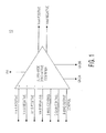
- FIG. 1
- is a functional diagram of the input and output signals of an ultra wide band active combiner, in accordance with an embodiment of the present invention;
- FIG. 2
- is a functional block diagram of the ultra wide band active combiner shown in FIG. 1, in accordance with an embodiment of the present invention;
- FIG. 3
- is a schematic diagram of a bandwidth peaking network and a core amplifier shown in FIG. 2, in accordance with an embodiment of the present invention;
- FIG. 4
- is a schematic diagram of a buffer shown in FIG. 2, in accordance with an embodiment of the present invention;
- FIG. 5
- is a schematic diagram of an output bias network shown in FIG. 2, in accordance with an embodiment of the present invention;
- FIG. 6
- is a schematic diagram of a core bias network shown in FIG. 2, in accordance with an embodiment of the present invention;
- FIG. 7
- is a schematic diagram of a common mode bias network and an impedance and voltage bias control network shown in FIG. 2, in accordance with an embodiment of the present invention;
- FIGS. 8 and 9
- are layouts showing the partitioning of transistors and resistors, which are located in a common centroid arrangement on a die, in accordance with an embodiment of the present invention;
- FIG. 10
- is a layout diagram showing approximate sizes of various elements of the ultra wide band active combiner of FIG. 2, in accordance with an embodiment of the present invention;
- FIG. 11A
- is a plot of impedance level (Z) versus frequency (in arbitrary units);
- FIG. 11B
- is a plot of gain (dBv) versus frequency (in arbitrary units); and
- FIG. 12
- is a detailed schematic diagram of the ultra wide band active combiner shown in FIGS. 1 and 2, in accordance with an embodiment of the present invention.
- As will be described, the present invention provides an ultra wide band active combiner, providing gain while operating between direct current (DC) and frequencies greater than 20 GHz. The present invention includes a bandwidth peaking network that extends the frequency response of the combiner and provides a substantially constant gain across that frequency response. In addition, the present invention receives two pairs of differential input signals and transmits one pair of differential output signals. The present invention also has controlled input impedances and a controlled output impedance. Moreover, the present invention operates with a low supply voltage and includes a common mode biasing method for alternating current (AC) applications, and an accurate fixed ratio bias tracking scheme. These features all contribute to advantageous improvements of an ultra wide band active combiner that provides amplification and is disposed on a die fabricated for use in an integrated circuit (IC) or chip.
- Referring to FIG. 1, there is shown a functional input/output block diagram of an ultra wide band active combiner, generally designated as 10. In accordance with an embodiment of the present invention, ultra wide band active combiner 10 includes two pairs of differential input signals, respectively shown as Vin A positive and Vin A negative and Vin B positive and Vin B negative. The ultra wide band
active combiner 10 also includes differential output signals, shown as Vout positive and Vout negative. The ultra wide bandactive combiner 10 also includes biasing controls, shown as current (I)-bias output control, I-bias control, and I-gain adjust. These different biasing and gain adjust controls will be described later. Lastly, as shown in FIG. 1, ultra wide bandactive combiner 10 includes a VCC primary power input of nominally 3.0 volts and GNDA and GNDB ground potentials. - A functional block diagram of the ultra wide band active combiner is shown in FIG. 2. As shown, ultra wide band
active combiner 10 includescore amplifier 18, which receives the positive input signals (Vin A pos and Vin B pos) and the negative input signals (Vin A neg and Vin B neg), being two pairs of differential input signals. The pair of differential output signals fromcore amplifier 18, namely the core positive output signal (core out pos) and the core negative output signal (core out neg) are buffered bybuffer 22 to provide the positive output signal (Vout pos) and negative output signal (Vout neg). - The biasing of the transistors of core amplifier 18 (shown in FIG. 3) is provided by
core bias network 24, which in turn is controlled by two input control signals of I-bias control and I-gain adjust. Biasing of the transistors of buffer 22 (shown in FIG. 4) is provided byoutput bias network 26, which in turn is controlled by an input signal of I-bias output control. -
Core amplifier 18 provides a gain adjusted, constant amplification of 10dBv across an ultra wide frequency band spanning from zero (DC) up to at least 20 GHz. The gain value ofcore amplifier 18 is maintained across the entire band of the combiner by use of bandwidth (BW) peakingnetwork 14. - Ultra wide band
active combiner 10 also includes tightly controlled input and output impedances. The input impedances are controlled by way of impedance and voltagebias control network 12, which in turn receives a voltage bias control feedback signal from commonmode bias network 16. The commonmode bias network 16 senses the voltage across the output terminals ofcore amplifier 18, as shown in FIG. 2. As will be described later, commonmode bias network 16 includes a center tap node, which feeds back a common mode voltage to the impedance and voltagebias control network 12 at the input terminals of ultra wide bandactive combiner 10. Consequently, the same voltage bias value is supplied to the positive input terminal and the negative input terminal for both pairs of input signals. - Referring next to FIG. 3, there is shown greater detail of
core amplifier 18 andbandwidth peaking network 14. In the embodiment shown in FIG. 3, transistors Q1 and Q76 are physically two separate transistors on the die; it will be appreciated, however, that transistors Q1 and Q76 behave as one transistor (it is noted that the bases of the transistors are connected; the collectors of the transistors are connected; and the emitters of the transistors are connected). Similarly, transistors Q2 and Q19 behave as one transistor; transistors Q65 and Q64 behave as one transistor; transistors Q67 and Q66 behave as one transistor; transistors Q95 and Q94 behave as one transistor; transistors Q97 and Q96 behave as one transistor; transistors Q74 and Q73 behave as one transistor; and transistors Q71 and Q72 behave as one transistor. - A negative input signal for a first input (Vin A neg) is provided into
core amplifier 18 by way of the bases of transistors Q1 and Q76; and a positive input signal for the first input (Vin A pos) is provided intocore amplifier 18 by way of the bases of transistors Q2 and Q19. A negative input signal for a second input (Vin B neg) is provided intocore amplifier 18 by way of the bases of transistors Q95 and Q94; and a positive input signal for the second input (Vin B pos) is provided intocore amplifier 18 by way of the bases of transistors Q96 and Q97. The output signals, namely the core out negative signal and the core out positive signal are provided as output differential signals by way of, respectively, the emitters of transistors Q73 and Q74, and the emitters of transistors Q71 and Q72, which in turn are respectively connected to the collectors of transistors Q65 and Q64 and transistors Q67 and Q66. In this manner,core amplifier 18 effectively provides a differential output signal. - The biasing of the transistors of
core amplifier 18 is provided by way of core bias network 24 (FIG. 6). As shown in FIG. 3, the emitters of transistors Q1, Q76, Q19 and Q2 are connected tocore bias network 24. Each of these four emitters is biased by the same bias current (Ic55). Similarly, the emitters of transistors Q65, Q64, Q67 and Q66 are connected tocore bias network 24. Each of these four emitters is biased by the same bias current (Ic68). Similarly, the emitters of transistors Q95, Q94, Q97 and Q96 are connected tocore bias network 24. Each of these four emitters is biased by the same bias current (Ic98). - The collector output current from the combination of transistors Q1 and Q76 is provided as an input current into the bases of the combination of transistors Q64 and Q65. The collector output current from the combination of transistors Q94 and Q95 is also provided as an input current into the bases of the combination of transistors Q64 and Q65. In a similar manner, the collector output current from the combination of transistors Q2 and Q19 is provided as an input current into the bases of the combination of transistors Q66 and Q67; and the collector output current from the combination of transistors Q96 and Q97 is also provided as an input current into the bases of the combination of transistors Q66 and Q67. In this manner, the two pairs of differential input signals are combined.
- The current flowing from the collectors of transistors Q65 and Q64 is provided to a first set of a resistor and inductor combination, namely R0 and L1 of the
bandwidth peaking network 14. Similarly, the collector current provided by the combination of transistors Q67 and Q66 flows through a second set of a resistor and inductor combination, namely R1 and L2 ofbandwidth peaking network 14. Another resistor (designated as R21), which is disposed between a node of R0 and L1 and another node of R1 and L2, is also configured to receive current from transistors Q64, Q65, Q66 and Q67. - It will be appreciated that the current flowing in the collectors of Q65 and Q64, and the current flowing in the collectors of Q67 and Q66, start rolling-off at a first predetermined frequency. On the other hand, with
bandwidth peaking network 14 included in the present invention, as shown in FIG. 3, the impedance seen at the collectors of Q64, Q65, Q66 and Q67 increases with frequency compensating for the collector current roll-off. - The inventor has discovered that, preferably by experimentation, the gain provided by
core amplifier 18 may be adjusted to have a substantially constant gain level from its lowest frequency response up to its maximum frequency response. This phenomenon is best shown by referring to FIGS. 11A and 11 B. FIG. 11A provides a plot of impedance (Z) seen by the collectors of Q64, Q65, Q66 and Q67 versus frequency in arbitrary units. The inventor has shown thatbandwidth peaking network 14 increases the frequency response of ultra wide bandactive combiner 10 by as much as 35 percent. For example, if one unit is defined as 11 GHz, then 1.35 units is at 15 GHz and, correspondingly, the upper frequency response of ultra wide bandactive combiner 10 is also at 15 GHz. As another example, if one unit is defined as 16 GHz, then 1.35 units is at 21.5 GHz and, correspondingly, the upper frequency response of ultra wide bandactive combiner 10 is also at 21.5 GHz. - In operation,
bandwidth peaking network 14 provides a substantially constant impedance level of Z up to 1.0 frequency units. From 1.0 frequency units up to 1.35 frequency units, the impedance level of Z increases, as shown in FIG. 11A. As a result, the gain ofcore amplifier 18, resulting from the combination of transistors Q64, Q65, Q66 and Q67 extends at a substantially constant value until reaching the frequency of 1.35 units, as shown in FIG. 11B. - The inventor has found that preferably R0 has a value and physical construction that is similar to the value and physical construction of R1. Furthermore, resistor R21 is substantially similar in value and physical construction to either resistor R0 or R1. Additionally, transistors Q64, Q65, Q66 and Q67 are preferably silicon germanium (SiGe) transistors which have a maximum transition frequency of 120 GHz. It will be appreciated that at the lower frequencies,
bandwidth peaking network 14 presents an impedance that is substantially resistive in value. This is due to L1 and L2 having an inductive low impedance at the lower frequencies. Consequently, R0 and R1 are effectively directly connected to VCC, which results in R21 being free of any current flow. - It will be understood that the number and values of the components of
bandwidth peaking network 14 on the die of the integrated circuit are complex. This is because there are many parasitic capacitances that exist between points across each physical resistor and points on the substrate of the die. Similarly, there are many parasitic capacitances that exist between points of each coil and points on the substrate. The impedance level Z varies as a function of frequency and is very complicated to calculate. As a result, the inventor prefers to find the resistive values of R0, R1 and R21 and the inductive values of L1 and L2 (which are equal to each other by symmetry) by experimentation. By experimentally adjusting the output gain response ofcore amplifier 18 to be at a constant gain of 10dBv, across the entire frequency bandwidth the values of R0, R1, R21, L1 and L2 may be determined. - The manner in which the gain of
core amplifier 18 is maintained at a constant value may be seen from the following simplified equations:


where:
gm(w) is the transconductance of the transistor as a function of frequency (ω),
Z(w) is the impedance presented to the transistor, and
Vout/Vin is the gain of the combiner. - The values of Z(w) presented to
core amplifier 18 by the bandwidth peaking network 14 (which includes resistances, inductances, and parasitic capacitances) are adjusted so that the gain of the ultra wide bandactive combiner 10 is maintained at a constant value over the desired frequency range. - Still referring to FIG. 3, there is shown resistor R12 connected between the collectors of transistor combination Q1 and Q76 and the emitters of transistor combination Q73 and Q74. Similarly, resistor R13 is connected between the collectors of the combination of transistors Q2 and Q19 and the emitters of the combination of transistors Q71 and Q72.
- The positive core output and the negative core output differential signals are buffered by buffer 22 (FIG. 2), before the positive voltage output and negative voltage output differential signals are transmitted from ultra wide band
active combiner 10.Buffer 22 is shown in more detail in FIG. 4. As shown,buffer 22 includes two transistors, designated as Q83 and Q85. The collector of each of these transistors is connected to VCC (nominally 3.0 volts), the base of each transistor receives one of the differential output signals fromcore amplifier 18, and the emitter of each transistor is biased by output bias network 26 (FIG. 2). The final differential output signals, namely Vout positive and Vout negative are provided by the emitters of Q83 and Q85, respectively. Thus, Q83 and Q85 behave as emitter followers and provide a gain value of less than one to the differential output signals ofcore amplifier 18. - The biasing of the emitters of transistors Q83 and Q85 is shown in greater detail in FIG. 5. As shown,
output bias network 26 provides a current bias to transistors Q83 and Q85 of buffer 22 (FIGS. 2 and 4). A collector current flowing in transistor Q84 is shown designated as lc84 and biases the emitter of transistor Q83 of buffer 22 (FIGS. 2 and 4). Similarly, a collector current flowing in transistor Q86 is shown designated as lc86 and biases the emitter of transistor Q85 of buffer 22 (FIGS. 2 and 4). It will be appreciated that the bases of transistors Q84 and Q86 are connected to each other and similarly controlled by the input signal of I-bias output control provided to transistor Q80. As shown, transistor Q80 has its collector and base connected together and coupled into output biasing transistors Q84 and Q86. Accordingly, the collector current of each of transistors Q84 and Q86 is substantially the same and the biases seen by the transistors ofbuffer 22 are substantially equal to each other. - More generally,
output bias network 26 may include N biasing transistors in a chain, as shown. Each of the N biasing transistors have their bases connected together and coupled to input transistor Q80. The input signal of I-bias output control, which controls each transistor in the chain, may be used to set equal bias values to other transistors (not shown) in an output buffer stage (for example, buffer 22). - Having described
output bias network 26,core bias network 24 will now be described. Referring to FIG. 6, there is showncore bias network 24. As shown, the core bias network is controlled by two input signals. The first input signal is I-bias control, which, for example, may have a nominal value of 500µA in this embodiment. The second input signal is I-gain adjust, which, for example, may have a value of 10µA per dB of gain reduction with a nominal range of 0 to 100µA for a combiner gain of 10dBv. The I-bias control signal is provided to the base of transistor Q0 by way of a compensation network of R5 and C330, which prevent oscillation of Q0. Transistor Q8 and resistor R14 are bleeding elements and prevent gain slope reversal that may happen for large values of I-gain adjust. - The bases of transistors Q55, Q68 and Q98 (and up to transistor Qn) are connected to the junction of R2 and R14. As a result, each of these biasing transistors provides the same biasing current to respective transistors of
core amplifier 18. As shown, biasing transistor Q55 provides biasing current Ic55 to transistors Q1, Q76, Q19 and Q2 ofcore amplifier 18. Similarly, biasing transistor Q68 provides biasing current Ic68 to transistors Q65, Q64, Q67 and Q66 ofcore amplifier 18. Also similarly, transistor Q98 provides biasing current Ic98 to transistors Q95, Q94, Q97 and Q96 ofcore amplifier 18. Transistors Q55, Q68 and Q98 provide bias current related to their physical size relationship with respect to reference transistor Q7. In general, there may be additional core biasing transistors placed in a chain (up to Qn), which may be used to bias additional transistors (not shown) of another exemplary core amplifier. - In operation, an increase in 1-bias control provides additional current flowing through the collector of the biasing transistors (Q55, Q68, Q98, up to Qn) which, in turn provide an increase in collector current flowing into
core amplifier 18. In this manner, an increase in 1-bias control results in an increase in gain ofcore amplifier 18. - Working in an opposite manner, an increase in 1-gain adjust results in an increased IR voltage drop across resistor R2 and a decreased IR drop across resistor R14. Consequently, as I-gain adjust increases, the current flowing into Q55, Q68, Q98, up to Qn decreases in value. This, in turn, causes a decrease in the collector currents of biasing transistors Q55, Q68, Q98, up to Qn. A decrease in the collector currents of these biasing transistors reduces the gain of
core amplifier 18. -
Core biasing network 24 may include biasing transistors (for example Q55, Q68, Q98, up to Qn) that provide corresponding collector currents (for example lc55, lc68, lc98, up to lcn) that are different from each other. As an example, transistor Q68 may be required to provide a collector current of lc68 at a value of 2mA, whereas transistor Q55 may be required to provide a collector current of lc55 at a value of 1mA. Such biasing ratio of 2mA/1mA may be achieved by implementing transistor Q68 physically twice as large as transistor Q55. As another example, transistor Q68 may be required to provide a collector current lc68 at a value of 4mA, whereas transistor Q55 may be required to provide a collector current lc55 at a value of 1mA. Such biasing ratio of 4mA/1mA may be achieved by implementing transistor Q68 physically four times larger than transistor Q55. In this manner, the present invention can maintain the desired biasing currents tocore amplifier 18 at a fixed ratio based upon the physical size relationship among the biasing transistors. - Referring next to FIG. 7, the common mode bias network, designated as 16, and the impedance and voltage bias control network, designated as 12, will now be described.
- The differential output from core amplifier 18 (FIG. 2), namely the voltage difference between the core out positive signal and the core out negative signal, is sensed by common
mode bias network 16 by way of resistor R36A and resistor R36B. Since the signal voltage across R36A and R36B is equal in magnitude but opposite in sign,node 17A is effectively a virtual ground (Vg) and includes the common mode voltage generated between the positive signal output (core out positive) and the negative signal output (core out negative). This common mode voltage atnode 17A is sensed by (or fed back to) node 17B as the voltage bias control feedback signal. - In operation, common
mode bias network 16 senses the differential output voltage ofcore amplifier 18 and establishes a common center point as the common mode voltage. The common mode voltage is fed back to impedance and voltagebias control network 12. The common mode voltage is split by way of resistors R42 and R43, and resistors R57 and R58 to establish a common voltage bias at both pairs of input terminals (nodes 17C and 17D) to core amplifier 18 (transistors Q1, Q76, Q19 and Q2, and transistors Q95, Q94, Q97 and Q96, shown in FIG. 3). - The input impedance across the input A terminals is controlled by
network 12 by way of resistor R8, which is connected between resistors R42 and R43. Since the impedance level looking back fromcore amplifier 18 has a high value, resistor R8 effectively establishes the impedance value at the input terminals of Vin A positive and Vin A negative. In the exemplary embodiment, the impedance level is 100 ohms betweennodes 17C and 17D, and the impedance level is 50 ohms between each terminal and ground potential. - Similarly, the input impedance across the input B terminals is controlled by
network 12 by way of resistor R24, which is connected between resistors R57 and R58. Since the impedance level looking back fromcore amplifier 18 has a high value, resistor R24 effectively establishes the impedance value at the input terminals of Vin B positive and Vin B negative. In the exemplary embodiment, the impedance level is 100 ohms betweennodes - It will be understood that ultra wide band
active combiner 10 is entirely fabricated on a substrate of a die for use as an integrated circuit. The layout of the various components shown in FIG. 2 is complex and configured using CAD tools. A functional high level block diagram of the die, generally designated as 100, is shown in FIG. 10. It will be understood that FIG. 10 is not drawn to scale and much of the layout detail is not shown. The die 100 of the integrated circuit includes an area of approximately 1000 microns by 1000 microns. The input and output pads (designated as 111, 119 and 127, 121 and 103, 117) as well as the voltage and ground pads (not shown) are approximately 100 microns by 100 microns each. - The Y-shaped lines shown in FIG. 10 are the input transmission lines for input A (designated as 113 and 115), which are disposed between the input A pads (111, 119) and the core amplifier (designated as 109). Similarly, the Y-shaped input transmission lines for input B (designated as 125 and 123) are disposed between the input B pads (127, 121) and
core amplifier 109. Also similarly, the Y-shaped output transmission lines (designated as 105 and 107) are disposed between the output buffer (shown as part of core 109) and the output voltage pads (103, 117). Also shown in FIG. 10 is the bandwidth peaking network (designated as 101), which is physically larger thancore 109. Thecore 109 has a size of approximately 100 microns by 30 microns. - Each of the transmission lines has a controlled impedance of 50 ohms. The width of each transmission line is approximately 25 microns.
- It will be appreciated that the transistors and the resistors are configured on the die to have a common centroid arrangement. For example, the transistors shown schematically in FIG. 3, namely the four groupings of Q1, Q76, Q19 and Q2; transistors Q95, Q94, Q97 and Q96; transistors Q64, Q65, Q66 and Q67; and transistors Q74, Q73, Q71 and Q72 are arranged as shown in FIG. 8. The arrangement of these transistors is shown designated generally as 80. Similarly, the resistors of common
mode bias network 16, shown schematically in FIG. 7, are also configured on the die in a common centroid arrangement. As shown in FIG. 9, one half of resistor R36B is disposed in the first quadrant ofarrangement 90 and the other half of resistor R36B is disposed in the third quadrant ofarrangement 90. Similarly, resistor R36A is divided in half as shown, where one half is disposed in the second quadrant and the other half is disposed in the fourth quadrant. - FIG. 12 depicts the ultra wide band active combiner in greater detail. As shown, ultra wide band
active combiner 1200 includes impedance and voltagebias control network 1202 and common mode bias network 1206 (previously described by reference to FIG. 7). Also shown in FIG. 12 is abandwidth peaking network 1204 and core amplifier 1210 (previously described by reference to FIG. 3).Buffer 1212 and output bias network 1214 (previously described, respectively, by reference to FIGS. 4 and 5) are shown on the right hand side of FIG. 12. Lastly,core bias network 1208 is shown at the bottom portion of FIG. 12 (previously described by reference to FIG. 6). - Also shown in FIG. 12 are connections from each transistor to the substrate of the die, connections from each resistor to the substrate, connections from each coil to the substrate, and connections from each capacitor to the substrate. These connections have been omitted in the other figures of ultra wide band
active combiner 10. The ultra wide band active combiner shown in FIG. 12 is implemented using selective-epitaxial SiGe bipolar transistors. The transistors shown in FIG. 12 may also be implemented using other materials including, but not limited to silicon, GaAs, InP and AlGaAs. - Although the invention is illustrated and described herein with reference to specific embodiments, the invention is not intended to be limited to the details shown. Rather, various modifications may be made in the details within the scope and range of equivalents of the claims and without departing from the invention.
Claims (20)
- A wideband combiner (10) comprising
a core amplifier (18) for receiving first and second pairs of differential input signals (VinA, VinB), and providing a single pair of differential output signals,
wherein the pair of differential output signals are a combination of the first pair and the second pair of differential input signals, and
a signal gain is implemented between the received first and second pairs of differential input signals and the single pair of differential output signals. - The wideband combiner (10) of claim 1, wherein
the core amplifier (18) is configured to provide a gain value between the first and second pairs of differential input signals and the single pair of differential output signals. - The wideband combiner (10) of claim 2, wherein
the gain is substantially constant across a frequency bandwidth response of the core amplifier. - The wideband combiner (10) of claim 2 or 3, wherein the gain is adjustable.
- The wideband combiner (10) of claim at least one of claims 1 to 4,
wherein
the frequency bandwidth response is between DC and at least 20 GHz. - The wideband combiner (10) of claim 1 further including
a bandwidth peaking network (14) including (a) a first coil (L1) and a first resistor (R0) connected in series and (b) a second coil (L2) and a second resistor (R1) connected in series,
the first coil and resistor and the second coil and resistor, respectively, coupled to the core amplifier for receiving amplified differential signals, and
the bandwidth peaking network configured to increase the frequency bandwidth of the amplifier. - The wideband combiner (10) of claim 6, wherein
the bandwidth peaking network (14) includes (a) a first node formed between the first coil and resistor and (b) a second node formed between the second coil and resistor,
a third resistor (R21) is connected between the first node and the second node, and
the third resistor is free-of current flow at low frequency operation of the core amplifier. - The wideband combiner (10) of claim 1 further including
a common mode bias network (16) coupled between output terminals providing the single pair of differential output signals and input terminals providing the first and second pairs of differential input signals, and
the common mode bias network providing a voltage bias control feedback signal from the output terminals to the input terminals,
wherein the voltage bias control feedback signal provides a virtual ground common mode potential. - The wideband combiner (10) of claim 8, wherein
the common mode potential across the input terminals is substantially equal to a DC potential across the output terminals. - A wideband combiner (10) of claim 6 or 7 wherein
the core amplifier including a first amplifier and a second amplifier for receiving the first and second pairs of differential input signals,
the first amplifier coupled to an end of the first resistor and the second amplifier coupled to an end of the second resistor, - The wideband combiner (10) of claim 10 wherein
the first and second amplifiers each includes:first and second stages of amplification, and(a) the first and second stages of amplification of the first amplifier and(b) the first and second stages of amplification of the second amplifier are configured as physically similar to each other on a die. - The wideband combiner (10) of claim 11 wherein
the first stage of amplification of the first amplifier and the first stage of amplification of the second amplifier are formed in at least one common centroid configuration on the die, and
the second stage of amplification of the first amplifier and the second stage of amplification of the second amplifier are formed in another common centroid configuration on the die. - The wideband combiner (10) of claim 11 wherein
the first stage of amplification of the first amplifier and the first stage of amplification of the second amplifier are biased by one common voltage reference point, and
the second stage of amplification of the first amplifier and the second stage of amplification of the second amplifier are biased by the same common voltage reference point. - The wideband combiner (10) of claim 13 wherein
the common voltage reference point includes a voltage level provided into bases of a plurality of transistors, and
a first collector of the plurality of transistors supplies a first collector current for biasing the first stages of amplification, and
a second collector of the plurality of transistors supplies a second collector current for biasing the second stages of amplification. - The wideband combiner (10) of claim 14 wherein
the first collector current and the second collector current are substantially similar to each other. - The wideband combiner (10) of claim 14 wherein
the first collector current and the second collector current are proportional to each other, based on a ratio of the physical sizes on the die of the respective transistor supplying the first collect current and the respective transistor supplying the second collector current. - The wideband combiner (10) of claim 14 wherein
current levels of the first and second collector currents are adjustable, and
the current levels are adjustable to provide a gain amount that is adjustable for the core amplifier. - The wideband combiner (10) of claim 11 wherein
the first stage of amplification includes a dual set of transistors, and
each set of transistors receive one pair of the first and second pairs of differential input signals. - A wideband combiner (10) comprising
a core amplifier (18) for receiving first and second pairs of differential input signals across input terminals and providing a single pair of differential output signals across output terminals,
the core amplifier (18) including a first amplifier and a second amplifier for receiving the first and second pairs of differential input signals,
a bandwidth peaking network (14) including (a) a first coil and a first resistor connected in series and (b) a second coil and a second resistor connected in series, (c) a first node formed between the first coil and the first resistor and a second node formed between the second coil and the second resistor, and (d) a third resistor connected between the first node and the second node,
the first amplifier coupled to an end of the first resistor and the second amplifier coupled to an end of the second resistor, and
a common mode bias network (16) coupled between the output terminals for providing a voltage bias control feedback signal across the input terminals,
wherein the bandwidth peaking network is configured to increase the frequency bandwidth of the core amplifier,
the core amplifier provides a substantially constant signal gain between the received single pair of differential input signals and the first and second pairs of differential output signals, and
the voltage bias control feedback signal provides a virtual ground common mode potential. - The wideband combiner (10) of claim 19 wherein
the common mode potential across the input terminals is substantially equal to a DC potential across the output terminals, and
the differential pair of input signals and the first and second pairs of differential output signals have substantially the same DC voltage bias.
Applications Claiming Priority (2)
| Application Number | Priority Date | Filing Date | Title |
|---|---|---|---|
| US81750906P | 2006-06-29 | 2006-06-29 | |
| US11/504,430 US7668522B2 (en) | 2006-06-29 | 2006-08-15 | Ultra wide band, differential input/output, high frequency active combiner in an integrated circuit |
Publications (3)
| Publication Number | Publication Date |
|---|---|
| EP1873911A2 true EP1873911A2 (en) | 2008-01-02 |
| EP1873911A3 EP1873911A3 (en) | 2008-03-12 |
| EP1873911B1 EP1873911B1 (en) | 2009-12-16 |
Family
ID=38659620
Family Applications (1)
| Application Number | Title | Priority Date | Filing Date |
|---|---|---|---|
| EP07110451A Active EP1873911B1 (en) | 2006-06-29 | 2007-06-18 | Ultra-wide band differential input/output, high frequency active combiner in an integrated circuit |
Country Status (4)
| Country | Link |
|---|---|
| US (1) | US7668522B2 (en) |
| EP (1) | EP1873911B1 (en) |
| AU (1) | AU2007202689B2 (en) |
| DE (1) | DE602007003780D1 (en) |
Citations (8)
| Publication number | Priority date | Publication date | Assignee | Title |
|---|---|---|---|---|
| US5489872A (en) * | 1994-01-25 | 1996-02-06 | Texas Instruments Incorporated | Transconductance-capacitor filter circuit with current sensor circuit |
| EP1003281A2 (en) * | 1998-11-19 | 2000-05-24 | Sony Corporation | Multi-input differential amplifier circuit |
| EP1083655A2 (en) * | 1999-09-10 | 2001-03-14 | Kabushiki Kaisha Toshiba | Amplifier circuit |
| EP1130771A1 (en) * | 2000-02-29 | 2001-09-05 | Fuji Photo Film Co., Ltd. | Amplifier circuit for a physical random number generator and a random number generator using the same |
| US6292033B1 (en) * | 2000-10-11 | 2001-09-18 | Intersil Corporation | Precision, low-power transimpedance circuit with differential current sense inputs and single ended voltage output |
| EP1306970A2 (en) * | 2001-10-25 | 2003-05-02 | Broadcom Corporation | Current-controlled CMOS wideband amplifier circuits |
| WO2003049282A1 (en) * | 2001-11-29 | 2003-06-12 | Infineon Technologies Ag | Fully-differentiated differential amplifier with high input impedance |
| US20050264356A1 (en) * | 2004-05-28 | 2005-12-01 | Cornell Research Foundation, Inc. | Extended bandwidth amplifier and oscillator using positive current feedback through inductive load |
Family Cites Families (4)
| Publication number | Priority date | Publication date | Assignee | Title |
|---|---|---|---|---|
| US5532637A (en) * | 1995-06-29 | 1996-07-02 | Northern Telecom Limited | Linear low-noise mixer |
| US7035616B2 (en) * | 2002-01-04 | 2006-04-25 | International Business Machines Corporation | Two-stage variable-gain mixer employing shunt feedback |
| DE10359867A1 (en) * | 2003-12-18 | 2005-07-14 | Endress + Hauser Gmbh + Co. Kg | coupling |
| US7403758B2 (en) * | 2005-10-04 | 2008-07-22 | Freescale Semicondutor, Inc. | Linearized and balanced mixer apparatus and signal mixing method |
-
2006
- 2006-08-15 US US11/504,430 patent/US7668522B2/en active Active
-
2007
- 2007-06-12 AU AU2007202689A patent/AU2007202689B2/en active Active
- 2007-06-18 EP EP07110451A patent/EP1873911B1/en active Active
- 2007-06-18 DE DE602007003780T patent/DE602007003780D1/en active Active
Patent Citations (8)
| Publication number | Priority date | Publication date | Assignee | Title |
|---|---|---|---|---|
| US5489872A (en) * | 1994-01-25 | 1996-02-06 | Texas Instruments Incorporated | Transconductance-capacitor filter circuit with current sensor circuit |
| EP1003281A2 (en) * | 1998-11-19 | 2000-05-24 | Sony Corporation | Multi-input differential amplifier circuit |
| EP1083655A2 (en) * | 1999-09-10 | 2001-03-14 | Kabushiki Kaisha Toshiba | Amplifier circuit |
| EP1130771A1 (en) * | 2000-02-29 | 2001-09-05 | Fuji Photo Film Co., Ltd. | Amplifier circuit for a physical random number generator and a random number generator using the same |
| US6292033B1 (en) * | 2000-10-11 | 2001-09-18 | Intersil Corporation | Precision, low-power transimpedance circuit with differential current sense inputs and single ended voltage output |
| EP1306970A2 (en) * | 2001-10-25 | 2003-05-02 | Broadcom Corporation | Current-controlled CMOS wideband amplifier circuits |
| WO2003049282A1 (en) * | 2001-11-29 | 2003-06-12 | Infineon Technologies Ag | Fully-differentiated differential amplifier with high input impedance |
| US20050264356A1 (en) * | 2004-05-28 | 2005-12-01 | Cornell Research Foundation, Inc. | Extended bandwidth amplifier and oscillator using positive current feedback through inductive load |
Non-Patent Citations (3)
| Title |
|---|
| ARAI T ET AL: "A GM-C FILTER USING MULTIPLE-OUTPUT LINEARIZED TRANSCONDUCTORS" IEICE TRANSACTIONS ON FUNDAMENTALS OF ELECTRONICS, COMMUNICATIONS AND COMPUTER SCIENCES, ENGINEERING SCIENCES SOCIETY, TOKYO, JP, vol. E87-A, no. 2, February 2004 (2004-02), pages 384-389, XP001047695 ISSN: 0916-8508 * |
| HUANG S-C ET AL INSTITUTE OF ELECTRICAL AND ELECTRONICS ENGINEERS: "A CMOS DIFFERENTIAL DIFFERENCE AMPLIFIER WITH RAIL-TO-RAIL FULLY-DIFFERENTIAL OUTPUTS" PROCEEDINGS OF THE MIDWEST SYMPOSIUM ON CIRCUITS AND SYSTEMS. LAFAYETTE, AUG. 3 - 5, 1994, NEW YORK, IEEE, US, vol. VOL. 2 SYMP. 37, 3 August 1994 (1994-08-03), pages 780-781, XP000531791 ISBN: 0-7803-2429-3 * |
| LAKSHMIKUMAR K R ET AL: "A CMOS ANALOG FRONT-END PROCESSOR FOR AN FDM SYSTEM" PROCEEDINGS OF THE CUSTOM INTEGRATED CIRCUITS CONFERENCE. BOSTON, MAY 13 - 16, 1990, NEW YORK, IEEE, US, vol. CONF. 12, 13 May 1990 (1990-05-13), pages 1241-1245, XP000167687 * |
Also Published As
| Publication number | Publication date |
|---|---|
| US7668522B2 (en) | 2010-02-23 |
| US20080032648A1 (en) | 2008-02-07 |
| AU2007202689A1 (en) | 2008-01-17 |
| EP1873911B1 (en) | 2009-12-16 |
| AU2007202689B2 (en) | 2010-11-25 |
| EP1873911A3 (en) | 2008-03-12 |
| DE602007003780D1 (en) | 2010-01-28 |
Similar Documents
| Publication | Publication Date | Title |
|---|---|---|
| EP1873909B1 (en) | Ultra wide band, differental Input/output , high frequency active splitter in an integrated circuit | |
| EP2056448B1 (en) | Low noise amplifier and differential amplifier | |
| US20130147548A1 (en) | Linear amplifier that perform level shift and method of level shifting | |
| EP1873910B1 (en) | Ultra-wide band differential input/output high frequency amplifier in an integrated circuit | |
| JP2006270466A (en) | Bias circuit for amplifier circuit | |
| US8971365B2 (en) | Symmetrical, direct coupled laser drivers | |
| US6642741B2 (en) | Electronically adjustable integrated circuit input/output termination method and apparatus | |
| EP1914887B1 (en) | Differential amplifier with current source controlled through differential feedback | |
| CN101162893B (en) | Variable gain amplifiers and relative transduction unit | |
| US20110294446A1 (en) | Gyrator circuit, wide-band amplifier and radio communication apparatus | |
| EP1873904A1 (en) | Ultra-wide band differential input/output, high frequency amplifier in an integrated circuit | |
| EP1873911B1 (en) | Ultra-wide band differential input/output, high frequency active combiner in an integrated circuit | |
| US20040124927A1 (en) | Transimpedance amplification apparatus with source follower structure | |
| JP5750178B1 (en) | Output circuit | |
| US6593814B2 (en) | Amplifier circuit with protective device | |
| US20230095506A1 (en) | Amplifier circuit, differential amplifier circuit, reception circuit, and semiconductor integrated circuit | |
| US11588476B2 (en) | Amplitude modulation circuit and semiconductor integrated circuit for optical communication system | |
| JP2607678B2 (en) | Differential amplifier circuit | |
| US8299854B2 (en) | Circuit for power amplification of an input signal and signal emission system incorporating such a circuit | |
| JPH0870222A (en) | Variable gain amplifier circuit | |
| JPH0865071A (en) | Agc circuit |
Legal Events
| Date | Code | Title | Description |
|---|---|---|---|
| PUAI | Public reference made under article 153(3) epc to a published international application that has entered the european phase |
Free format text: ORIGINAL CODE: 0009012 |
|
| AK | Designated contracting states |
Kind code of ref document: A2 Designated state(s): AT BE BG CH CY CZ DE DK EE ES FI FR GB GR HU IE IS IT LI LT LU LV MC MT NL PL PT RO SE SI SK TR |
|
| AX | Request for extension of the european patent |
Extension state: AL BA HR MK YU |
|
| PUAL | Search report despatched |
Free format text: ORIGINAL CODE: 0009013 |
|
| AK | Designated contracting states |
Kind code of ref document: A3 Designated state(s): AT BE BG CH CY CZ DE DK EE ES FI FR GB GR HU IE IS IT LI LT LU LV MC MT NL PL PT RO SE SI SK TR |
|
| AX | Request for extension of the european patent |
Extension state: AL BA HR MK YU |
|
| 17P | Request for examination filed |
Effective date: 20080415 |
|
| AKX | Designation fees paid |
Designated state(s): DE FR GB |
|
| GRAP | Despatch of communication of intention to grant a patent |
Free format text: ORIGINAL CODE: EPIDOSNIGR1 |
|
| RTI1 | Title (correction) |
Free format text: ULTRA-WIDE BAND DIFFERENTIAL INPUT/OUTPUT, HIGH FREQUENCY ACTIVE COMBINER IN AN INTEGRATED CIRCUIT |
|
| GRAS | Grant fee paid |
Free format text: ORIGINAL CODE: EPIDOSNIGR3 |
|
| GRAA | (expected) grant |
Free format text: ORIGINAL CODE: 0009210 |
|
| AK | Designated contracting states |
Kind code of ref document: B1 Designated state(s): DE FR GB |
|
| REG | Reference to a national code |
Ref country code: GB Ref legal event code: FG4D |
|
| REF | Corresponds to: |
Ref document number: 602007003780 Country of ref document: DE Date of ref document: 20100128 Kind code of ref document: P |
|
| PLBE | No opposition filed within time limit |
Free format text: ORIGINAL CODE: 0009261 |
|
| STAA | Information on the status of an ep patent application or granted ep patent |
Free format text: STATUS: NO OPPOSITION FILED WITHIN TIME LIMIT |
|
| 26N | No opposition filed |
Effective date: 20100917 |
|
| PGFP | Annual fee paid to national office [announced via postgrant information from national office to epo] |
Ref country code: DE Payment date: 20110629 Year of fee payment: 5 |
|
| REG | Reference to a national code |
Ref country code: GB Ref legal event code: 732E Free format text: REGISTERED BETWEEN 20120906 AND 20120912 |
|
| REG | Reference to a national code |
Ref country code: DE Ref legal event code: R081 Ref document number: 602007003780 Country of ref document: DE Owner name: EXELIS INC. (N. D. GES. D. STAATES INDIANA), US Free format text: FORMER OWNER: ITT MANUFACTURING ENTERPRISES, INC., WILMINGTON, US Effective date: 20120817 |
|
| REG | Reference to a national code |
Ref country code: FR Ref legal event code: TP Owner name: EXELIS INC., US Effective date: 20120912 Ref country code: FR Ref legal event code: CD Owner name: EXELIS INC., US Effective date: 20120912 |
|
| REG | Reference to a national code |
Ref country code: DE Ref legal event code: R119 Ref document number: 602007003780 Country of ref document: DE Effective date: 20130101 |
|
| PG25 | Lapsed in a contracting state [announced via postgrant information from national office to epo] |
Ref country code: DE Free format text: LAPSE BECAUSE OF NON-PAYMENT OF DUE FEES Effective date: 20130101 |
|
| REG | Reference to a national code |
Ref country code: FR Ref legal event code: PLFP Year of fee payment: 10 |
|
| REG | Reference to a national code |
Ref country code: FR Ref legal event code: PLFP Year of fee payment: 11 |
|
| REG | Reference to a national code |
Ref country code: FR Ref legal event code: PLFP Year of fee payment: 12 |
|
| PGFP | Annual fee paid to national office [announced via postgrant information from national office to epo] |
Ref country code: FR Payment date: 20230626 Year of fee payment: 17 |
|
| PGFP | Annual fee paid to national office [announced via postgrant information from national office to epo] |
Ref country code: GB Payment date: 20230627 Year of fee payment: 17 |