EP1873875A2 - Laser-diode pumped solid state laser apparatus, optical scanning apparatus, image forming apparatus and display apparatus - Google Patents
Laser-diode pumped solid state laser apparatus, optical scanning apparatus, image forming apparatus and display apparatus Download PDFInfo
- Publication number
- EP1873875A2 EP1873875A2 EP07252620A EP07252620A EP1873875A2 EP 1873875 A2 EP1873875 A2 EP 1873875A2 EP 07252620 A EP07252620 A EP 07252620A EP 07252620 A EP07252620 A EP 07252620A EP 1873875 A2 EP1873875 A2 EP 1873875A2
- Authority
- EP
- European Patent Office
- Prior art keywords
- laser
- laser light
- state laser
- pumped solid
- diode pumped
- Prior art date
- Legal status (The legal status is an assumption and is not a legal conclusion. Google has not performed a legal analysis and makes no representation as to the accuracy of the status listed.)
- Granted
Links
Images













Classifications
-
- H—ELECTRICITY
- H01—ELECTRIC ELEMENTS
- H01S—DEVICES USING THE PROCESS OF LIGHT AMPLIFICATION BY STIMULATED EMISSION OF RADIATION [LASER] TO AMPLIFY OR GENERATE LIGHT; DEVICES USING STIMULATED EMISSION OF ELECTROMAGNETIC RADIATION IN WAVE RANGES OTHER THAN OPTICAL
- H01S3/00—Lasers, i.e. devices using stimulated emission of electromagnetic radiation in the infrared, visible or ultraviolet wave range
- H01S3/09—Processes or apparatus for excitation, e.g. pumping
- H01S3/091—Processes or apparatus for excitation, e.g. pumping using optical pumping
- H01S3/094—Processes or apparatus for excitation, e.g. pumping using optical pumping by coherent light
- H01S3/0941—Processes or apparatus for excitation, e.g. pumping using optical pumping by coherent light of a laser diode
-
- H—ELECTRICITY
- H01—ELECTRIC ELEMENTS
- H01S—DEVICES USING THE PROCESS OF LIGHT AMPLIFICATION BY STIMULATED EMISSION OF RADIATION [LASER] TO AMPLIFY OR GENERATE LIGHT; DEVICES USING STIMULATED EMISSION OF ELECTROMAGNETIC RADIATION IN WAVE RANGES OTHER THAN OPTICAL
- H01S3/00—Lasers, i.e. devices using stimulated emission of electromagnetic radiation in the infrared, visible or ultraviolet wave range
- H01S3/005—Optical devices external to the laser cavity, specially adapted for lasers, e.g. for homogenisation of the beam or for manipulating laser pulses, e.g. pulse shaping
-
- H—ELECTRICITY
- H01—ELECTRIC ELEMENTS
- H01S—DEVICES USING THE PROCESS OF LIGHT AMPLIFICATION BY STIMULATED EMISSION OF RADIATION [LASER] TO AMPLIFY OR GENERATE LIGHT; DEVICES USING STIMULATED EMISSION OF ELECTROMAGNETIC RADIATION IN WAVE RANGES OTHER THAN OPTICAL
- H01S3/00—Lasers, i.e. devices using stimulated emission of electromagnetic radiation in the infrared, visible or ultraviolet wave range
- H01S3/05—Construction or shape of optical resonators; Accommodation of active medium therein; Shape of active medium
- H01S3/06—Construction or shape of active medium
- H01S3/0602—Crystal lasers or glass lasers
- H01S3/0604—Crystal lasers or glass lasers in the form of a plate or disc
-
- H—ELECTRICITY
- H01—ELECTRIC ELEMENTS
- H01S—DEVICES USING THE PROCESS OF LIGHT AMPLIFICATION BY STIMULATED EMISSION OF RADIATION [LASER] TO AMPLIFY OR GENERATE LIGHT; DEVICES USING STIMULATED EMISSION OF ELECTROMAGNETIC RADIATION IN WAVE RANGES OTHER THAN OPTICAL
- H01S3/00—Lasers, i.e. devices using stimulated emission of electromagnetic radiation in the infrared, visible or ultraviolet wave range
- H01S3/05—Construction or shape of optical resonators; Accommodation of active medium therein; Shape of active medium
- H01S3/06—Construction or shape of active medium
- H01S3/0602—Crystal lasers or glass lasers
- H01S3/061—Crystal lasers or glass lasers with elliptical or circular cross-section and elongated shape, e.g. rod
-
- H—ELECTRICITY
- H01—ELECTRIC ELEMENTS
- H01S—DEVICES USING THE PROCESS OF LIGHT AMPLIFICATION BY STIMULATED EMISSION OF RADIATION [LASER] TO AMPLIFY OR GENERATE LIGHT; DEVICES USING STIMULATED EMISSION OF ELECTROMAGNETIC RADIATION IN WAVE RANGES OTHER THAN OPTICAL
- H01S3/00—Lasers, i.e. devices using stimulated emission of electromagnetic radiation in the infrared, visible or ultraviolet wave range
- H01S3/05—Construction or shape of optical resonators; Accommodation of active medium therein; Shape of active medium
- H01S3/06—Construction or shape of active medium
- H01S3/0602—Crystal lasers or glass lasers
- H01S3/0612—Non-homogeneous structure
-
- H—ELECTRICITY
- H01—ELECTRIC ELEMENTS
- H01S—DEVICES USING THE PROCESS OF LIGHT AMPLIFICATION BY STIMULATED EMISSION OF RADIATION [LASER] TO AMPLIFY OR GENERATE LIGHT; DEVICES USING STIMULATED EMISSION OF ELECTROMAGNETIC RADIATION IN WAVE RANGES OTHER THAN OPTICAL
- H01S3/00—Lasers, i.e. devices using stimulated emission of electromagnetic radiation in the infrared, visible or ultraviolet wave range
- H01S3/05—Construction or shape of optical resonators; Accommodation of active medium therein; Shape of active medium
- H01S3/06—Construction or shape of active medium
- H01S3/0602—Crystal lasers or glass lasers
- H01S3/0617—Crystal lasers or glass lasers having a varying composition or cross-section in a specific direction
-
- H—ELECTRICITY
- H01—ELECTRIC ELEMENTS
- H01S—DEVICES USING THE PROCESS OF LIGHT AMPLIFICATION BY STIMULATED EMISSION OF RADIATION [LASER] TO AMPLIFY OR GENERATE LIGHT; DEVICES USING STIMULATED EMISSION OF ELECTROMAGNETIC RADIATION IN WAVE RANGES OTHER THAN OPTICAL
- H01S3/00—Lasers, i.e. devices using stimulated emission of electromagnetic radiation in the infrared, visible or ultraviolet wave range
- H01S3/05—Construction or shape of optical resonators; Accommodation of active medium therein; Shape of active medium
- H01S3/06—Construction or shape of active medium
- H01S3/0627—Construction or shape of active medium the resonator being monolithic, e.g. microlaser
-
- H—ELECTRICITY
- H01—ELECTRIC ELEMENTS
- H01S—DEVICES USING THE PROCESS OF LIGHT AMPLIFICATION BY STIMULATED EMISSION OF RADIATION [LASER] TO AMPLIFY OR GENERATE LIGHT; DEVICES USING STIMULATED EMISSION OF ELECTROMAGNETIC RADIATION IN WAVE RANGES OTHER THAN OPTICAL
- H01S3/00—Lasers, i.e. devices using stimulated emission of electromagnetic radiation in the infrared, visible or ultraviolet wave range
- H01S3/09—Processes or apparatus for excitation, e.g. pumping
- H01S3/091—Processes or apparatus for excitation, e.g. pumping using optical pumping
- H01S3/094—Processes or apparatus for excitation, e.g. pumping using optical pumping by coherent light
- H01S3/09408—Pump redundancy
-
- H—ELECTRICITY
- H01—ELECTRIC ELEMENTS
- H01S—DEVICES USING THE PROCESS OF LIGHT AMPLIFICATION BY STIMULATED EMISSION OF RADIATION [LASER] TO AMPLIFY OR GENERATE LIGHT; DEVICES USING STIMULATED EMISSION OF ELECTROMAGNETIC RADIATION IN WAVE RANGES OTHER THAN OPTICAL
- H01S3/00—Lasers, i.e. devices using stimulated emission of electromagnetic radiation in the infrared, visible or ultraviolet wave range
- H01S3/14—Lasers, i.e. devices using stimulated emission of electromagnetic radiation in the infrared, visible or ultraviolet wave range characterised by the material used as the active medium
- H01S3/16—Solid materials
- H01S3/1601—Solid materials characterised by an active (lasing) ion
- H01S3/1603—Solid materials characterised by an active (lasing) ion rare earth
- H01S3/1611—Solid materials characterised by an active (lasing) ion rare earth neodymium
-
- H—ELECTRICITY
- H01—ELECTRIC ELEMENTS
- H01S—DEVICES USING THE PROCESS OF LIGHT AMPLIFICATION BY STIMULATED EMISSION OF RADIATION [LASER] TO AMPLIFY OR GENERATE LIGHT; DEVICES USING STIMULATED EMISSION OF ELECTROMAGNETIC RADIATION IN WAVE RANGES OTHER THAN OPTICAL
- H01S3/00—Lasers, i.e. devices using stimulated emission of electromagnetic radiation in the infrared, visible or ultraviolet wave range
- H01S3/23—Arrangements of two or more lasers not provided for in groups H01S3/02 - H01S3/22, e.g. tandem arrangements of separate active media
- H01S3/2383—Parallel arrangements
-
- H—ELECTRICITY
- H01—ELECTRIC ELEMENTS
- H01S—DEVICES USING THE PROCESS OF LIGHT AMPLIFICATION BY STIMULATED EMISSION OF RADIATION [LASER] TO AMPLIFY OR GENERATE LIGHT; DEVICES USING STIMULATED EMISSION OF ELECTROMAGNETIC RADIATION IN WAVE RANGES OTHER THAN OPTICAL
- H01S3/00—Lasers, i.e. devices using stimulated emission of electromagnetic radiation in the infrared, visible or ultraviolet wave range
- H01S3/23—Arrangements of two or more lasers not provided for in groups H01S3/02 - H01S3/22, e.g. tandem arrangements of separate active media
- H01S3/2383—Parallel arrangements
- H01S3/2391—Parallel arrangements emitting at different wavelengths
Definitions
- the present invention generally relates to laser-diode pumped solid-state laser apparatuses, optical scanning apparatuses, image forming apparatuses and display apparatuses. More particularly, the present invention relates to a laser-diode pumped solid-state laser apparatus having a solid-state laser crystal in which pumping is caused by laser diode. Further, the present invention relates to any of an optical scanning apparatus, an image forming apparatus or a display apparatus that uses such a laser-diode pumped solid-state laser apparatus.
- lasers are used in various fields including laser printers and laser measuring instruments. Further, aiming practical application in future, investigation and development are being made with regard to laser display apparatus or the like. In such apparatuses that use laser light, there is an increasing demand for downsizing of laser source and improvement of laser light quality.
- Patent Reference 1 discloses a solid-state laser oscillation apparatus that uses a laser medium having a doped part and undoped part.
- Patent Reference 2 discloses a laser apparatus having a gain medium and a waveguide of pumping light
- Patent Reference 3 discloses a laser apparatus having a laser medium and a waveguide optical system.
- Patent Reference 4 discloses a method of manufacturing an oxide monocrystal (single crystal) having a core part and a cladding part
- Patent Reference 5 discloses an oxide monocrystal of fiber shape for optical applications formed of a fiber body of an oxide monocrystal and a liquid-phase epitaxial layer of an oxide monocrystal formed so as to cover the surface of the foregoing fiber body.
- Patent Reference 6 discloses a solid-state laser crystal in which doping concentration of laser-activating ions is increased continuously or stepwise from an end surface where excitation is caused toward an end surface where cooling is made.
- Patent Reference 7 discloses a composite laser device having a transparent crystal body including therein a region where laser oscillation can take place and a second crystal body jointed to the transparent crystal body, wherein at least one of the transparent crystal body and the second crystal body is formed of a polycrystalline material.
- Patent Reference 8 discloses a solid-state laser oscillator having a polycrystalline ceramic composite laser medium in which a polycrystalline transparent ceramic not containing active element and a polycrystalline transparent ceramic doped with an active element are jointed.
- Non-Patent Reference 1 disclose a composite monocrystal that has regions formed by so-called dual-die EFG (edge-defined film-fed growth) process with different compositions or components.
- the present invention has been made in view of the foregoing problems and it is a first aim of the present invention to provide a laser-diode pumped solid-state laser apparatus capable of providing high-quality laser output without increasing the size of the source.
- a second, optional, aim of the present invention is to provide an optical scanning apparatus capable of scanning a surface with high precision.
- a third, optional, aim of the present invention is to provide an image forming apparatus capable of forming high-quality images.
- a fourth, optional, aim of the present invention is to provide a display apparatus capable ot displaying information with high display quality.
- the present invention provides a laser-diode pumped solid-state laser apparatus, comprising:
- At least one laser light generator used therein comprises the monocrystalline substance doped with the dopant element (optical emission center: rare earth element or transitional metal element) excited by the pumping laser light from the at least one laser diode, with the concentration profile such that the dopant element increases a concentration thereof from near zero concentration gently in the form of a slope in the direction perpendicular to the laser oscillation direction, it is easily possible to attain the desired distribution of optical absorption in the monocrystalline substance. Further, there is no need with the present invention to shape the excitation laser light, and it becomes possible to provide a laser output of high beam quality, without inviting increase of size of the solid-state laser apparatus.
- the dopant element optical emission center: rare earth element or transitional metal element
- the present invention provides an optical scanning apparatus scanning a surface by an optical beam, wherein the optical scanning apparatus comprises at least one laser-diode pumped solid-state laser apparatus of the present invention for producing the optical beam.
- the optical scanning apparatus comprises at least one laser-diode pumped solid-state laser apparatus as set forth above, it becomes possible to scan the surface with the optical beam with high precision as a result.
- the present invention provides an image forming apparatus forming an image on an object by using a laser light, wherein the image forming apparatus comprises at least one laser-diode pumped solid-state laser apparatus as set forth above for producing the laser light.
- the image forming apparatus comprises at least one laser-diode pumped solid-state laser apparatus as set forth above, it becomes possible to form high-quality images as a result.
- the present invention provides a display apparatus displaying information by using laser light, wherein the display apparatus comprises at least one laser-diode pumped solid-state laser apparatus as set forth above for producing the laser light.
- the display apparatus comprises at least one laser-diode pumped solid-state laser apparatus as set forth above, it becomes possible to attain high-quality display of information as a result.
- Figures 1A and 1B show the schematic construction of a laser-diode pumped solid-state laser apparatus 100 according to a first embodiment of the present invention.
- explanation will be made based on the coordinate system in which Z-axis is chosen in the laser oscillation direction and X and Y-axes are chosen in a plane perpendicular to the Z-axis with mutually perpendicular relationship.
- the laser-diode pumped solid-state laser apparatus 100 of the present embodiment is an apparatus of so-called side-pumped type and includes two laser diode array elements LDa and LDb for the purpose of pumping, a solid-state laser crystal 10, an output mirror 40, and a heat sink 30.
- the two laser diode array elements LDa and LDb are disposed on the +Z-side of the heat sink 30 in a manner so as to face each other in the Y-axis direction, wherein each of the laser diode array elements LDa and LDb produces a pumping laser light of the wavelength of 808nm with the output power of 40W.
- the laser diode array LDa emits the pumping laser light in the +Y direction while the laser diode array LDb produces the pumping laser light in the -Y direction.
- each of the optical systems 20a and 20b is formed by a combination of plural lenses and is disposed on the +Z side of the heat sink 30.
- the optical system 20a is deposed at the +Y side of the laser diode array LDa and focuses the pumping laser light therefrom.
- the optical system 20b is deposed at the -Y side of the laser diode array LDb and focuses the pumping laser light therefrom.
- the solid-state laser crystal 10 is disposed on the +Z side of the heat sink 30 at the +Y side of the optical system 20a and at the -Y side of the optical system 20b.
- the solid-state laser crystal 10 may be a uniaxial monocrystal of gadolinium vanadate (GdVO 4 ) having a disk shape (or chip shape), wherein it should be noted that the solid-state laser crystal 10 is doped with neodymium (Nd) as the dopant element (emission center) excited by the pumping laser light from the laser-diode array elements.
- GdVO 4 gadolinium vanadate
- Nd neodymium
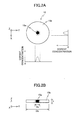
- the concentration profile of Nd has a sloped shape in which the Nd concentration increases gradually from near zero concentration in the direction perpendicular to the direction of laser oscillation (Z-axis direction in the present case).
- core part 10a the part contributing to laser oscillation
- cladding part 10b the part scarcely contributing to laser oscillation
- the solid-state laser crystal 10 is integrally formed of the core part 10a and the cladding part 10b.
- the core part 10a is a circular part of a diameter Da located at a central part of the solid-state laser crystal.
- the cladding part 10b is a donut shaped part surrounding the core part 10a.
- the concentration of Nd in the core part 10a becomes maximum near the center of the core part 10a and decreases gradually toward the cladding part 10b.
- the Nd concentration near the center of the core part 10a is about 0.5at%, where within this application at% is determined by the ratio: (number of atoms of dopant)/(number of atoms of host material).
- the Nd concentration profile has a shape resembling a Gauss distribution profile.
- the solid-state laser crystal 10 is formed by slicing a rod-shaped moncrystal (columnar crystal) ingot manufactured by the dual-die EFG process explained before or by a ⁇ PD process and may have a thickness t of 0.5mm, a diameter Db of 5mm and a diameter Da of 1mm. It should be noted that the solid-state laser crystal 10 is a crystal that is designed to emit a laser light of linear polarization upon excitation by optical pumping.
- the surface of the solid-state laser crystal 10 at the side where the heat sink 30 is provided (the surface at -Z side, designated as "A surface” for the sake of convenience) is provided with a coating providing a reflectance of 99.9% for the light of a wavelength of 1063nm.
- the surface of the solid-state laser crystal 10 at the side opposite to the side where the heat sink 30 is provided (the surface at +Z side, designated as "B surface” for the sake of convenience) is provided with a coating providing a transmittance of 99.9% for the light of the wavelength of 1063nm.
- a metal layer 32 of Cr/Ni/Au laminated structure On the surface of the coating at the A surface, there is formed a metal layer 32 of Cr/Ni/Au laminated structure, wherein the metal layer 32 is jointed to an Au-Sn alloy layer 31 formed on the heat sink 30.
- This output mirror 40 has a radius of curvature of 5000mm at the -Z side surface and has a transmittance of 5% to the light of the wavelength of 1063nm.
- the distance between the A surface of the solid-state laser crystal 10 and surface of the output mirror 40 at the -Z side is set to 100mm. Further, the laser light forms a beam of the beam diameter of 0.5mm inside the solid-state laser crystal 10.
- the output mirror 40 may have a so-called microchip construction integrated with the solid-state laser crystal 10.
- the laser diode array LDa emits a pumping laser light with the wavelength of 808nm, wherein the emitted pumping laser light is injected into the solid-state laser crystal 10 at a side surface thereof after passing through the optical system 20a.
- the laser diode array LDb emits a pumping laser light with the wavelength of 808nm, wherein the emitted pumping laser light is injected into the solid-state laser crystal 10 at a side surface thereof after passing through the optical system 20b.
- the Nd dopant in the solid-state laser crystal 10 undergoes excitation by the pumping laser light and there is caused laser oscillation by the cavity 35 formed by the A surface of the solid-state laser crystal 10 and the output mirror 40 (see Figure 3) with the wavelength of 1063nm. That laser light of the wavelength of 1063nm is then emitted after passing through the output mirror 40.
- the laser-diode pumped solid-state laser apparatus 100 of the first embodiment is thus provided with the solid-state laser crystal 10 that includes a uniaxial monocrystal of gadolinium vanadate (GdVO 4 ) doped with Nd, which undergoes excitation by the pumping laser lights from the two pumping laser diode array elements LDa and LDb, wherein Nd is doped with such a concentration profile that the concentration of Nd increases gradually in the sloped shape from near zero concentration in the direction perpendicular to the laser oscillation direction (Z-axis direction in the present example).
- GdVO 4 gadolinium vanadate
- the heat generated in the solid-state laser crystal 10, originating from the energy difference between the pumping laser light and the output laser light, is radiated directly via the A surface, and it becomes possible to suppress the temperature rise of the solid-state laser crystal 10. As a result, it becomes possible to achieve high power operation of the laser-diode pumped solid-state laser apparatus 100.
- the laser-diode pumped solid-state laser apparatus 100 of the first embodiment it is possible to optimize the heat distribution profile by adjusting the concentration profile of Nd in the solid-state laser crystal 10.
- the laser-diode pumped solid-state laser apparatus 100 of the first embodiment of the present invention it becomes possible to provide an output laser light of excellent beam quality without providing a correction mechanism for the change of refractive index (thermal lens effect).
- the laser-diode pumped solid-state laser apparatus 100 of the first embodiment it becomes possible to output a laser light of the wavelength of 1063nm with excellent beam quality and with high output power.
- the present invention is not limited to such a particular construction.
- the specification of coating of the solid-state laser crystal 10 and the optical properties of the output mirror 40 it is also possible to obtain an output laser light of the wavelength of 912nm or 1340nm.
- Nd dopant is substantially zero.
- concentration may be 0.001at% or less.
- the maximum of the Nd dopant concentration at the centre of the laser light generator may be 0.5at% when causing oscillation at the wavelength of 1064nm.
- the maximum value of the dopant concentration may be 0.25at%.
- the minimum of the dopant concentration at the centre of the laser light generator may be 0.2at%.
- the rate of change of the Nd dopant concentrations with distance may fall in the range of 0.03 - 0.07 at % / 0.05 mm. In one example, the rate of change is 0.06 at % / 0.05mm.
- Figure 8A shows the schematic construction of a laser-diode pumped solid-state laser apparatus 200 according to a second embodiment of the present invention.
- the laser-diode pumped solid-state laser apparatus 200 has a construction similar to that of the laser-diode pumped solid-state laser apparatus 100 of the first embodiment, except that there is disposed a non-linear optic crystal 50 on the optical path of the laser light between the solid-state layer crystal 10 and the output mirror 40 and that the optical properties of the output mirror 40 is different and the specification of the coating of the solid-state laser crystal 10 is different. Otherwise, the construction of the present embodiment is the same as the first embodiment.
- the non-linear optic crystal 50 converts the laser light of the wavelength of 1063nm of the fundamental mode to a laser light of the wavelength of 531.5nm forming a second harmonic mode.
- a PPMgLN device a device of LiNbO 3 having a periodically inversed polarization structure doped with MgO
- This non-linear optic crystal 50 has a length of 5mm (in the X-axis direction and Y-axis direction) and a thickness of 2mm (in the Z-axis direction).
- the non-linear optic crystal 50 is disposed with such an orientation that the crystal axis thereof points the direction in which there is attained a pseudo phase matching condition with the polarization direction of the laser light inside the cavity.
- a coating providing a transmittance of 99.5% or higher for both the fundamental mode light of the wavelength of 1063nm and the second harmonics light of the wavelength of 531.5nm.
- the surface at the -Z side of the non-linear optic crystal 50 will be designated as C surface, while the surface at the +Z side will be designated as D surface.
- a coating having a reflectance of 99.9% with regard to the light of the wavelength of 1063nm As shown in Figure 8B, there is provided a coating on the surface (B surface) opposite to the A surface of the solid-state laser crystal 10, such that the coating provides the transmittance of 99.9% for the light of the wavelength of 1063nm and the reflectance of 99% for the light of the wavelength of 531.5nm. With this, it is possible to suppress the incidence of the second harmonic wave generated inside the cavity to penetrate into the solid-state layer crystal 10.
- the output mirror 40 has a radius of curvature of 5000mm at the -Z side surface and has a reflectance of 99.9% to the light of the wavelength of 1063nm and the transmittance of 99% to the light of the wavelength of 531.5nm.
- the laser diode array LDa emits a pumping laser light with the wavelength of 808nm, wherein the emitted pumping laser light is injected into the solid-state laser crystal 10 at a side surface thereof after passing through the optical system 20a.
- the laser diode array LDb emits a pumping laser light with the wavelength of 808nm, wherein the emitted pumping laser light is injected into the solid-state laser crystal 10 at a side surface thereof after passing through the optical system 20b.
- the Nd dopant element in the solid-state laser crystal 10 undergoes excitation by the pumping laser light and there is caused laser oscillation by the cavity 35A formed by the A surface of the solid-state laser crystal 10 and the output mirror 40 (see Figure 8B) with the wavelength of 1063nm.
- the laser light of the wavelength of 1063nm is confined inside the cavity 35A and forms the fundamental mode.
- the non-linear optic element 50 is disposed inside the cavity 35A, the confined fundamental mode wave undergoes wavelength transition, resulting in generation of the second order harmonics, and the laser light of the wavelength of 531.5nm is formed as the second order harmonics, wherein this laser light of the wavelength of 531.5nm is outputted through the output mirror 40.
- the laser-diode pumped solid-state laser apparatus 200 of the second embodiment is thus provided with the solid-state laser crystal 10 that includes a uniaxial monocrystal of gadolinium vanadate (GdVO 4 ) doped with Nd, which undergoes excitation by the pumping laser lights from the two pumping laser diode array elements LDa and LDb, wherein Nd is doped with such a concentration profile that the concentration of Nd increases gently in the sloped shape from near zero concentration in the direction perpendicular to the laser oscillation direction (Z-axis direction in the present example).
- GdVO 4 gadolinium vanadate
- the laser-diode pumped solid-state laser apparatus 200 of the second embodiment in which it is possible to inject a high power laser light of excellent beam quality into the non-linear optic element 50, there is attained improvement of efficiency of conversion in the non-linear optic element 50.
- the laser-diode pumped solid-state laser apparatus 200 of the second embodiment it becomes possible to output a laser light of the wavelength of 531.5nm with excellent beam quality and with high output power, without inviting increase of size of the apparatus.
- the non-linear optic element 50 may have a length of 5mm and a thickness of 2nm, while the present invention is by no means limited to such a specific example.
- other construction may be used as long as the laser light of the fundamental mode having the wavelength of 1063nm is converted to the laser light of the second harmonics of the wavelength of 531.5nm with desired conversion efficiency.
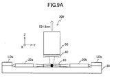
- Figure 9A shows the schematic construction of a laser-diode pumped solid-state laser apparatus 300 according to a third embodiment of the present invention.
- the laser-diode pumped solid-state laser apparatus 300 has a construction similar to that of the laser-diode pumped solid-state laser apparatus 200 of the second embodiment, except that the non-linear optic crystal 50 is disposed a the +Z side of the output mirror 40. Otherwise, the construction of the present embodiment is same to that of the second embodiment. Hereinafter, explanation will be made mainly on the difference over the second embodiment. Thereby, it should be noted that the same reference numerals are used for the parts identical to or equivalent to the parts of the second embodiment and the description thereof will be simplified or omitted.
- the non-linear optic element 50 is disposed on the optical_path of the laser light passed through the output mirror 40.
- This non-linear optic crystal 50 may have a thickness (length in the Z-axis direction) of 10mm, for example.
- the non-linear optic crystal 50 may have a small thickness in view of large optical intensity
- the non-linear optic element 50 is disposed outside the optical cavity, it is necessary to achieve the wavelength conversion with one pass of the laser light through the non-linear optic crystal 50,1 and thus, there is a need of increasing the thickness of the non-linear optic crystal 50 for attain the conversion efficiency comparable to that of the second embodiment.
- the laser-diode pumped solid-state laser apparatus 300 of the third embodiment in which the laser light of the wavelength of 1063nm of high power and excellent beam quality is injected into the non-linear optic element 50, it becomes possible to emit a laser light of the wavelength of 531.5nm with high beam quality and high output without inviting increase of size of the apparatus, similarly to the laser-diode pumped solid-state laser apparatus 200 according to the second embodiment of the present invention.
- the non-linear optic element 50 may have a length of 5mm and a thickness of 10nm, while the present invention is by no means limited to such a specific example.
- other construction may be used as long as the laser light of the fundamental mode having the wavelength of 1063nm is converted to the laser light of the second harmonics of the wavelength of 531.5nm with desired conversion efficiency.
- the laser-diode pumped solid-state laser apparatus 300 of the third embodiment it is also possible to dispose a lens between the output mirror 40 and the non-linear optic crystal 50. With this, it becomes possible to focus the fundamental mode wave incident to the non-linear optic element 50, resulting in improvement of beam strength of the fundamental wave, and the conversion efficiency in the non-linear optic crystal 50 is improved further as a result.
- Figure 10A shows the schematic construction of a laser-diode pumped solid-state laser apparatus 400 according to a fourth embodiment of the present invention.
- the laser-diode pumped solid-state laser apparatus 400 has a construction similar to that of the laser-diode pumped solid-state laser apparatus 200 of the second embodiment, except that the specification is changed for the coating on the D surface of the non-linear optic crystal 50 and that the output mirror 40 is eliminated. Otherwise, the construction of the present embodiment is same to that of the second embodiment. Hereinafter, explanation will be made mainly on the difference over the second embodiment. Thereby, it should be noted that the same reference numerals are used for the parts identical to or equivalent to the parts of the second embodiment and the description thereof will be simplified or omitted.
- a coating on the D surface of the non-linear optic crystal 50 wherein the coating thus provided has a reflectance of 99.9% for fundamental mode light of the wavelength of 1063nm and the transmittance of 99.5% for the second harmonics light of the wavelength of 531.5nm. Further, on the C surface of the non-linear optic crystal 50, there is provided a coating providing a transmittance of 99.5% or higher for both the fundamental mode light of the wavelength of 1063nm and the second harmonics light of the wavelength of 531.5nm.
- the solid-state laser crystal 10 and the non-linear optic element 50 are fixed with each other with simple contact or with a photo-resistive adhesive. Thereby, the solid-state laser crystal 10 and the non-linear optic crystal 50 may make an optical contact free from coating.
- the laser-diode pumped solid-state laser apparatus 400 of the fourth embodiment in which the laser light of the wavelength of 1063nm of high power and excellent beam quality is injected into the non-linear optic element 50, it becomes possible to emit a laser light of the wavelength of 531.5nm with high beam quality and high output without inviting increase of size of the apparatus, similarly to the laser-diode pumped solid-state laser apparatus 200 according to the second embodiment of the present invention.
- the laser-diode pumped solid-state laser apparatus 400 according to the fourth embodiment of the present invention, there is no need of providing the output mirror 40 used with the laser-diode pumped solid-state laser apparatus 200, and it becomes possible to facilitate size reduction further.
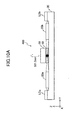
- Figure 11A shows the schematic construction of a laser-diode pumped solid-state laser apparatus 500 according to a fifth embodiment of the present invention.
- the laser-diode pumped solid-state laser apparatus 500 has a construction similar to that of the laser-diode pumped solid-state laser apparatus 300 of the second embodiment, except that the specification is changed for the solid-state laser crystal 10 and the non-linear optic crystal 50 and that the output mirror 40 is eliminated. Otherwise, the construction of the present embodiment is same to that of the third embodiment. Hereinafter, explanation will be made mainly on the difference over the third embodiment. Thereby, it should be noted that the same reference numerals are used for the parts identical to or equivalent to the parts of the third embodiment and the description thereof will be simplified or omitted.
- a coating having a reflectance of 99.9% with regard to the light of the wavelength of 1063nm as shown in Figure 11B. Further, as shown in Figure 11B, there is provided a coating having a transmittance of 5% with regard to the light of the wavelength of 1063nm on the B surface of the solid-state laser crystal 10.
- a coating having a transmittance of 99.5% or more for the second harmonics light of the wavelength of 531.5nm there are provided a coating having a transmittance of 99.5% or more for the second harmonics light of the wavelength of 531.5nm.
- the solid-state laser crystal 10 and the non-linear optic element 50 are fixed with each other with simple contact or with a photo-resistive adhesive. Thereby, the solid-state laser crystal 10 and the non-linear optic crystal 50 may make an optical contact free from coating.
- the laser-diode pumped solid-state laser apparatus 500 of the fifth embodiment in which the laser light of the wavelength of 1063nm of high power and excellent beam quality is injected into the non-linear optic element 50, it becomes possible to emit a laser light of the wavelength of 531.5nm with high beam quality and high output without inviting increase of size of the apparatus, similarly to the laser-diode pumped solid-state laser apparatus 300 according to the third embodiment of the present invention.
- the laser-diode pumped solid-state laser apparatus 500 according to the fifth embodiment of the present invention, there is no need of providing the output mirror 40 used with the laser-diode pumped solid-state laser apparatus 300, and it becomes possible to facilitate size reduction further.
- the present invention is not limited to such a particular construction.
- the pitch of polarization reversal or coating specification of the non-linear optic crystal 50 appropriately, it is also possible to obtain an output laser light of the wavelength of 670nm or 456nm.
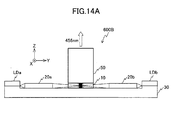
- Figure 12 shows the schematic construction of a laser-diode pumped solid-state laser apparatus 600 according to a sixth embodiment of the present invention.
- the laser-diode pumped solid-state laser apparatus 600 includes: a first solid-state_laser apparatus 600R emitting an output laser light of red color with the wavelength of 670nm; a second solid-state laser apparatus 600B emitting an output laser light of blue color with the wavelength of 456nm; and a third solid-state laser apparatus 600G emitting an output laser light of green color with the wavelength of 531.5nm.
- the first solid-state laser apparatus 600R has a construction similar to the laser-diode pumped solid-state laser apparatus 500 according to the fifth embodiment explained before.
- the non-linear optic crystal 50 is a PPMgLN device having a different pitch for the polarization reversal and carries a coating on the respective end surfaces thereof such that a transmittance of 99.5% or more is attained for the light of the wavelength of 1340nm and the light of the wavelength of 670nm.
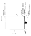
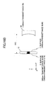
- the second solid-state laser apparatus 600B has a construction similar to the laser-diode pumped solid-state laser apparatus 500 according to the fifth embodiment explained before.
- the non-linear optic crystal 50 is a PPMgLN device having a different pitch for the polarization reversal and carries a coating on the respective end surfaces thereof such that a transmittance of 99.5% or more is attained for the light of the wavelength of 912nm and the light of the wavelength of 456nm.
- the third solid-state laser apparatus 600G has a construction similar to the laser-diode pumped solid-state laser apparatus 500 according to the fifth embodiment explained before.
- the laser-diode pumped solid-state laser apparatus 600 of the sixth embodiment including therein a plurality of solid-state laser apparatuses each having a solid-state laser crystal 10, to provide a plurality of laser output lights of high output power with excellent beam quality, without inviting increase of size of the laser apparatus 600.
- each of the solid-state laser apparatuses emits the laser light with the same wavelength.
- the laser-diode pumped solid-state laser apparatus 600 may include two solid-state laser apparatuses or four or more solid-state laser apparatuses.
- Figure 16A shows the schematic construction of a laser-diode pumped solid-state laser apparatus 700 according to a seventh embodiment of the present invention.
- the laser-diode pumped solid-state laser apparatus 700 is an apparatus of the edge pumping structure and includes a laser diode LD for pumping, a lens 20, the solid-state laser crystal 10 and the output mirror 40.
- the laser-diode LD is a device of single-stripe structure and can produce a laser light of the wavelength of 808nm with an output power of 2W.
- the laser diode LD emits a laser light in the +Z direction.
- the lens 20 is disposed at the +Z side of the laser diode LD and focuses the pumping laser light from the laser diode LD upon the solid-state laser crystal 10.
- the lens 20 may be the element capable of focusing the pumping laser light to form a beam with a beam diameter of about 1mm.
- the solid-state laser crystal 10 is disposed at the +Z side of the lens 20.
- the surface of the solid-state laser crystal 10 at the side where the lens 20 is provided (the surface at -Z side, designated as "E surface” for the sake of convenience) is provided with a coating providing a reflectance of 99.9% for the light of the wavelength of 808nm and a transmittance of 0.1% for the light of the wavelength of 1063nm.
- the surface of the solid-state laser crystal 10 at the side opposite to the E surface is provided with a coating providing a transmittance of 99.9% for the light of the_ wavelength of 1063nm.
- This output mirror 40 has a radius of curvature of 5000mm at the -Z side surface and has a transmittance of 5% to the light of the wavelength of 1063nm.
- the distance between the E surface of the solid-state laser crystal 10 and surface of the output mirror 40 at the -Z surface is set to 100mm. Further, the laser light forms a beam of the beam diameter of 0.5mm inside the solid-state laser crystal 10.
- the output mirror 40 may have a so-called microchip construction integrated with the solid-state laser crystal 10.
- the laser light (pumping laser light) of the wavelength of 808nm emitted from the laser diode LD passes through the lens 20 and enters into the solid-state crystal 10.
- the Nd dopant element in the solid-state laser crystal 10 undergoes excitation by the pumping laser light and there is caused laser oscillation by the cavity 35C formed by the E surface of the solid-state laser crystal 10 and the output mirror 40 with the wavelength of 1063nm. That laser light of the wavelength of 1063nm is then emitted after passing through the output mirror 40.
- the beam shape (spot shape) of the focused pumping laser light provides a profound influence on the beam quality of the laser light (output laser light) emitted from the laser-diode pumped solid-state laser apparatus.
- the laser-diode pumped solid-state laser apparatus 700 of the seventh embodiment thus provided with the solid-state laser crystal 10 that includes a uniaxial monocrystal of gadolinium vanadate (GdVO 4 ) doped with Nd, which undergoes excitation by the pumping laser lights from the pumping laser diode LD, wherein Nd is doped with such a concentration profile that the concentration of Nd increases gently in the sloped shape from near zero concentration in the direction perpendicular to the laser oscillation direction (X-axis direction in the present example).
- GdVO 4 gadolinium vanadate
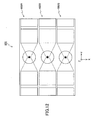
- the present invention is by no means limited to such a specific example, and thus, the solid-state laser crystal 10 may also be the one having a rectangular plate shape as shown in Figures 17A and 17B, wherein the solid-state laser crystal 10 of Figures 17A and 17B may be manufactured by cutting a periphery of a rod-shaped crystal ingot produced by a dual-die EFG process or ⁇ PD process, followed by a slicing process. Further, the solid-state laser crystal 10 may also have a polygonal shape.
- the present invention is not limited to such a specific example and it is also possible to use other rare earth element or metal ions. Further, the concentration of the dopant element is not limited to 0.5at%.
- the present invention is not limited to such a specific construction.
- the dimensions of the solid-state laser crystal 10 may be changed as needed according to the beam quality demanded for the output laser light.
- Figure 18 shows a schematic construction of a laser printer 1000 as an image forming apparatus according to an embodiment of the present invention.
- the laser printer 1000 comprises an optical scanning apparatus 900, a photosensitive drum 901, an electrostatic charger 902, a developing roller 903, a toner cartridge 904, a cleaning blade 905, a sheet feed tray 906, a sheet feed roller 907, resist roller pairs 908, a transfer charger 911, discharging unit 914, a fixing roller 909, a sheet discharging roller 912, a sheet discharging tray 910, and the like.
- the electrostatic charger 902, the developing roller 903, the transfer charger 911, the discharging unit 914 and the cleaning blade 905 are disposed in the vicinity of the photosensitive drum 901. Thereby, the electrostatic charger 902, the developing roller 903, the transfer charger 911, the discharging unit 914 and the cleaning blade 905 are disposed in the order of: electrostatic charger 902 ⁇ developing roller 903 ⁇ transfer charger 911 ⁇ discharging unit 914 ⁇ cleaning blade 905, along the rotating direction of the photosensitive drum 901.
- the photosensitive drum 901 carries thereon a photosensitive layer.
- the photosensitive drum 901 rotates in the clockwise direction (arrow direction) within the plane of Figure 18.
- the electrostatic charger 902 charges the surface of the photosensitive drum 901 uniformly.
- the optical scanning apparatus 900 irradiates a modulated light upon the surface of the photosensitive drum 901 charged with the electric charger 902 with modulation based upon the image information from upper hierarchy apparatus such as personal computer. With this, there is formed a latent image corresponding to the image information on the surface of the photosensitive drum 901. The latent image thus formed is moved in the direction of the developing roller 903 with rotation of the photosensitive drum 905. It should be noted that the elongating direction of the photosensitive drum 901 (direction along the rotational axis) is called “main scanning direction” and the rotational direction of the photosensitive drum 901 is called “sub-scanning direction”. This construction of this optical scanning apparatus 900 will be explained later.
- the toner cartridge 904 holds toners, and the toners are supplied therefrom to the developing roller 903.
- the developing roller 903 causes the toners supplied from the toner cartridge 904 to adhere to the latent image formed on the surface of the photosensitive drum 901, and with this, development of the image information is attained.
- the latent image thus formed is moved in the direction of the transfer charger 911 with rotation of the photosensitive drum 901.
- the sheet feed tray 906 accommodates therein recording sheets 913. Further, there is disposed a sheet feed roller 907 in the vicinity of the sheet feed tray 906, and the sheet feed roller 907 picks up the recording sheet 913 one by one from the sheet feed tray 906 and supplies the same to the resist roller pair 908.
- the resist roller pair 908 is disposed in the vicinity of the transfer roller 911 and holds the recording sheet 913 picked up by the sheet feed roller 907 temporarily and supplies the recording sheet to the gap between the photosensitive drum 901 and the transfer charger 911 in synchronization with the rotation of the photosensitive drum 901.
- the transfer charger 911 is applied with a voltage of reverse polarity to the toners for attracting the toners on the surface of the photosensitive drum 901 to the recording sheet 913 electrically. With this voltage, the toner image on the surface of the photosensitive drum 901 is transferred to the recording sheet 913. The recording sheet 913 thus transferred with the toner image is then forwarded to the fixing roller 909.
- the discharging unit 914 discharges the surface of the photosensitive drum 901.
- the cleaning blade 905 removes the toner (residual toner) remaining on the surface of the photosensitive drum 901. The residual toners thus removed are used again. After removal of the residual toners, the photosensitive drum 901 returns to the position of the electrostatic charger 902.
- the optical scanning apparatus comprises an optical source 11, a coupling lens 12, a modulator 17, a cylindrical lens 13, a polygonal mirror 14, a f ⁇ lens 15 a toroidal lens and a main controller not illustrated but used for controlling the foregoing various parts, wherein the optical source 11 includes a laser apparatus equivalent to any of the laser-diode pumped solid-state laser apparatus 100 - 500 and 700 explained previously.
- the coupling lens 12 shapes the optical beam emitted from the optical source 11 to form a generally parallel light.
- the modulator 17 turns on and off the optical beam passed through the coupling lens 12.
- the cylindrical lens 13 focuses the optical beam passed through the modulator 17 upon a reflection surface of the polygonal mirror 14.
- the polygonal mirror 14 has a right hexagonal pillar member of low profile and carries six deflection surfaces on the lateral side thereof. Further, the polygonal mirror 14 is rotated_at a constant angular velocity in the direction of arrow indicated in Figure 19. Thus, the optical beam emitted from the optical source 11 and is focused upon the deflection surface of the polygonal mirror 14 by the cylindrical lens 13 undergoes deflection with a constant angular velocity with rotation of the polygonal mirror 14.
- the f ⁇ lens 15 has an image height proportional to the incident angle of the optical beam from the polygonal mirror 14 and causes the image plane of the optical beam deflected by the polygonal mirror 14 with the constant angular velocity with an equal speed in the main scanning direction.
- the toroidal lens 16 focuses the optical beam passed through the f ⁇ lens 15 on the surface of the photosensitive drum 901.
- the optical scanning apparatus 900 of the present embodiment it becomes possible to scan the surface of the photosensitive drum 901 with high precision in view of the fact that the optical scanning apparatus 900 includes, for the optical source 11 thereof, a laser apparatus equivalent to any of the laser-diode pumped solid-state laser apparatuses 100 - 500 and 700.
- the laser printer 1000 of the present embodiment it becomes possible to form high-quality images in view of the fact that the laser printer 1000 includes the optical scanning apparatus 900, which in turn includes a laser-diode pumped solid laser apparatus equivalent to any of the laser-diode pumped solid laser apparatuses 100 - 500 or 700 noted before.
- the optical source 11 may include the foregoing laser apparatus in plural numbers. In such a case, it becomes possible to carry out plural scanning simultaneously, and as a result, it becomes possible to form images with high speed with the laser printer 1000.
- the deflection direction of the optical beam is controlled by controlling the deflection angle of the MEMS mirror.
- the present invention is by no means limited to this specific application.
- it becomes possible to form high-quality images with stability by using the laser apparatus equivalent to any of the laser-diode pumped solid-state laser apparatuses 100 - 500 or 700 for the image forming apparatus.
- the image forming apparatus may be the one that includes a laser apparatus equivalent to any of the laser-diode pumped solid-state laser apparatuses 100 - 700 and irradiates the laser beam directly to the medium such as a sheet that shows coloring with laser irradiation.
- Figure 20 shows a schematic construction of a laser display apparatus 2000 as a display apparatus according to an embodiment of the present invention.
- the laser display apparatus 2000 comprises an optical source 101, an optical system 103 including a mirror and directing a laser light from the optical source 101 to a screen 104, and a control apparatus 105 for controlling the optical source 101 and the optical system 103, wherein the optical source 101 includes a laser apparatus equivalent to any of the laser-diode pumped solid-state laser apparatuses 100 - 700.
- the laser display apparatus 2000 of the present embodiment it becomes possible to draw pictures or characters on the screen 104 with high quality as a result of use of any of the laser-diode pumped solid-state laser apparatuses 100 - 700 for the optical source of the laser light.
- the present invention also for the optical source 101, it is possible to improve the display effect with the laser display apparatus that performs image display by laser lights penetrating through the space.
- the laser-diode pumped solid-state laser apparatus can provide the laser light of excellent beam quality without inviting increase of size of the laser apparatus. Further, according to the optical scanning apparatus of the present invention, it becomes possible to scan a surface with high precision. Further, according to the image forming apparatus of the present invention, it becomes possible to form high-quality images. Further, according to the display apparatus of the present invention, it becomes possible to display information with high display quality.
- the present invention is based on Japanese priority application No.2006-178884 filed on June 29, 2006, the entirety of which is incorporated herein as reference.
Landscapes
- Physics & Mathematics (AREA)
- Electromagnetism (AREA)
- Engineering & Computer Science (AREA)
- Plasma & Fusion (AREA)
- Optics & Photonics (AREA)
- Lasers (AREA)
- Laser Beam Printer (AREA)
- Transforming Electric Information Into Light Information (AREA)
Abstract
Description
- The present invention generally relates to laser-diode pumped solid-state laser apparatuses, optical scanning apparatuses, image forming apparatuses and display apparatuses. More particularly, the present invention relates to a laser-diode pumped solid-state laser apparatus having a solid-state laser crystal in which pumping is caused by laser diode. Further, the present invention relates to any of an optical scanning apparatus, an image forming apparatus or a display apparatus that uses such a laser-diode pumped solid-state laser apparatus.
- These days, lasers are used in various fields including laser printers and laser measuring instruments. Further, aiming practical application in future, investigation and development are being made with regard to laser display apparatus or the like. In such apparatuses that use laser light, there is an increasing demand for downsizing of laser source and improvement of laser light quality.
- Various proposals have been made with regard to so-called solid-state lasers (see Patent References 1 - 11, for example).
- For example,
Patent Reference 1 discloses a solid-state laser oscillation apparatus that uses a laser medium having a doped part and undoped part. Further,Patent Reference 2 discloses a laser apparatus having a gain medium and a waveguide of pumping light, whilePatent Reference 3 discloses a laser apparatus having a laser medium and a waveguide optical system. - Further,
Patent Reference 4 discloses a method of manufacturing an oxide monocrystal (single crystal) having a core part and a cladding part, whilePatent Reference 5 discloses an oxide monocrystal of fiber shape for optical applications formed of a fiber body of an oxide monocrystal and a liquid-phase epitaxial layer of an oxide monocrystal formed so as to cover the surface of the foregoing fiber body. Further,Patent Reference 6 discloses a solid-state laser crystal in which doping concentration of laser-activating ions is increased continuously or stepwise from an end surface where excitation is caused toward an end surface where cooling is made. - Further,
Patent Reference 7 discloses a composite laser device having a transparent crystal body including therein a region where laser oscillation can take place and a second crystal body jointed to the transparent crystal body, wherein at least one of the transparent crystal body and the second crystal body is formed of a polycrystalline material. Further,Patent Reference 8 discloses a solid-state laser oscillator having a polycrystalline ceramic composite laser medium in which a polycrystalline transparent ceramic not containing active element and a polycrystalline transparent ceramic doped with an active element are jointed. - Further,
Parent References 11 andNon-Patent Reference 1 disclose a composite monocrystal that has regions formed by so-called dual-die EFG (edge-defined film-fed growth) process with different compositions or components. -
Patent Reference 1
Japanese Patent 3,503,588 -
Patent Reference 2
Japanese Laid-Open Patent Application 2004-356479 -
Patent Reference 3
Japanese Laid-Open Patent Application 2004-152817 -
Patent Reference 4
Japanese Patent 3759807 -
Patent Reference 5
Japanese Laid-Open Patent Application 8-278419 Patent Reference 6
Japanese Patent 3266071 -
Patent Reference 7
Japanese Laid-Open Patent Application 2005-327997 -
Patent Reference 8
Japanese Laid-Open Patent Application 2002-57388 Patent Reference 9
Japanese Laid-Open Patent Application 6-128089 Patent Reference 10
Japanese Laid-Open Patent Application 6-128076 Patent Reference 11
Japanese Laid-Open Patent Application 6-128078 - P. Rudolph, K. Shimamura and T. Fukuda, "The Radial Selectivity of In-situ Core-doped Crystal Rods Grown by the Double Die EFG Method, Cryst. Res. Technol. vol.29, 1994, No. 6, pp.801-807.
- However, with conventional laser optical sources, it has been difficult to obtain a high-quality laser light without increasing the size of the laser optical source.
- Thus, the present invention has been made in view of the foregoing problems and it is a first aim of the present invention to provide a laser-diode pumped solid-state laser apparatus capable of providing high-quality laser output without increasing the size of the source.
- A second, optional, aim of the present invention is to provide an optical scanning apparatus capable of scanning a surface with high precision.
- A third, optional, aim of the present invention is to provide an image forming apparatus capable of forming high-quality images.
- A fourth, optional, aim of the present invention is to provide a display apparatus capable ot displaying information with high display quality.
- In a first aspect, the present invention provides a laser-diode pumped solid-state laser apparatus, comprising:
- at least one laser diode producing a pumping laser light; and
- at least one laser light generator comprising a monocrystalline substance doped with a dopant element (optical emission center: rare earth element or transitional metal element) and pumped with said pumping laser light from said at least one laser diode,
- said monocrystalline substance containing said dopant element with a concentration profile such that said dopant element increases a concentration thereof in a direction perpendicular to a laser oscillation direction gently in the form of a slope from a near zero concentration.
- According to the present invention, in which at least one laser light generator used therein comprises the monocrystalline substance doped with the dopant element (optical emission center: rare earth element or transitional metal element) excited by the pumping laser light from the at least one laser diode, with the concentration profile such that the dopant element increases a concentration thereof from near zero concentration gently in the form of a slope in the direction perpendicular to the laser oscillation direction, it is easily possible to attain the desired distribution of optical absorption in the monocrystalline substance. Further, there is no need with the present invention to shape the excitation laser light, and it becomes possible to provide a laser output of high beam quality, without inviting increase of size of the solid-state laser apparatus.
- In a second aspect, the present invention provides an optical scanning apparatus scanning a surface by an optical beam, wherein the optical scanning apparatus comprises at least one laser-diode pumped solid-state laser apparatus of the present invention for producing the optical beam.
- According to the present invention, in which the optical scanning apparatus comprises at least one laser-diode pumped solid-state laser apparatus as set forth above, it becomes possible to scan the surface with the optical beam with high precision as a result.
- In a third aspect, the present invention provides an image forming apparatus forming an image on an object by using a laser light, wherein the image forming apparatus comprises at least one laser-diode pumped solid-state laser apparatus as set forth above for producing the laser light.
- According to the present invention, in which the image forming apparatus comprises at least one laser-diode pumped solid-state laser apparatus as set forth above, it becomes possible to form high-quality images as a result.
- In a fourth aspect, the present invention provides a display apparatus displaying information by using laser light, wherein the display apparatus comprises at least one laser-diode pumped solid-state laser apparatus as set forth above for producing the laser light.
- According to the present invention, in which the display apparatus comprises at least one laser-diode pumped solid-state laser apparatus as set forth above, it becomes possible to attain high-quality display of information as a result.
- The present invention will be described further below with reference to exemplary embodiments and the accompanying drawings, in which:
- Figures 1A and 1B are diagrams for explaining a laser-diode pumped solid-state laser apparatus according to a first embodiment of the present invention;
- Figures 2A and 2B are diagrams for explaining the solid-state laser crystal of Figures 1A and 1B;
- Figure 3 is a diagram for explaining a cavity in Figure 1A;
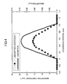
- Figure 4 is a diagram for explaining the absorption coefficient and absorption amount in the solid-state laser crystal of Figures 2A and 2B;
- Figure 5 is a diagram for explaining the absorption amount in the solid-state laser crystal of Figures 2A and 2B in a three-dimensional plot;
- Figure 6 is a diagram for explaining the absorption coefficient and absorption amount for the case of uniform Nd concentration in a core part;
- Figure 7 is a diagram for explaining the absorption amount in a three-dimensional plot for the case of uniform Nd concentration in a core part;
- Figures 8A and 8B are diagrams for explaining a laser-diode pumped solid-state laser apparatus according to a second embodiment of the present invention;
- Figures 9A and 9B are diagrams for explaining a laser-diode pumped solid-state laser apparatus according to a third embodiment of the present invention;
- Figures 10A and 10B are diagrams for explaining a laser-diode pumped solid-state laser apparatus according to a fourth embodiment of the present invention;
- Figures 11A and 11B are diagrams for explaining a laser-diode pumped solid-state laser apparatus according to a fifth embodiment of the present invention;
- Figure 12 is a diagram for explaining a laser-diode pumped solid-state laser apparatus according to a sixth embodiment of the present invention;
- Figures 13A and 13B are diagrams for explaining a solid-
state laser apparatus 600R of Figure 12; - Figures 14A and 14B are diagrams for explaining a solid-
state laser apparatus 600B of Figure 12; - Figures 15A and 15B are diagrams for explaining a solid-
state laser apparatus 600G of Figure 12; - Figures 16A and 16B are diagrams for explaining a laser-diode pumped solid-state laser apparatus according to a seventh embodiment of the present invention;
- Figures 17A and 17B are diagrams for explaining a modification of the solid-state laser crystal;
- Figure 18 is a diagram for explaining the schematic construction of a laser printer according to an embodiment of the present invention;
- Figure 19 is a diagram explaining the schematic construction of an optical scanning apparatus used in the laser printer of Figure 18;
- Figure 20 is a diagram for explaining a laser printer according to an embodiment of the present invention.
- Hereinafter, a laser-diode pumped solid-state laser apparatus according to a first embodiment of the present invention will be described.
- Figures 1A and 1B show the schematic construction of a laser-diode pumped solid-
state laser apparatus 100 according to a first embodiment of the present invention. In the present invention, explanation will be made based on the coordinate system in which Z-axis is chosen in the laser oscillation direction and X and Y-axes are chosen in a plane perpendicular to the Z-axis with mutually perpendicular relationship. - Referring to Figures 1A and 1B, the laser-diode pumped solid-
state laser apparatus 100 of the present embodiment is an apparatus of so-called side-pumped type and includes two laser diode array elements LDa and LDb for the purpose of pumping, a solid-state laser crystal 10, anoutput mirror 40, and aheat sink 30. - The two laser diode array elements LDa and LDb are disposed on the +Z-side of the
heat sink 30 in a manner so as to face each other in the Y-axis direction, wherein each of the laser diode array elements LDa and LDb produces a pumping laser light of the wavelength of 808nm with the output power of 40W. In the illustrated example, the laser diode array LDa emits the pumping laser light in the +Y direction while the laser diode array LDb produces the pumping laser light in the -Y direction. - Further, there are provided two
optical systems optical systems heat sink 30. Thereby, it becomes possible to form an optical spot on the incident surface of the solid-state laser crystal 100 with a size of 100µm (in the thickness direction of the solid-state laser crystal 10: Z-axis direction) x 1000µm (X-axis direction). Here, theoptical system 20a is deposed at the +Y side of the laser diode array LDa and focuses the pumping laser light therefrom. Further, theoptical system 20b is deposed at the -Y side of the laser diode array LDb and focuses the pumping laser light therefrom. - The solid-
state laser crystal 10 is disposed on the +Z side of theheat sink 30 at the +Y side of theoptical system 20a and at the -Y side of theoptical system 20b. - As shown in Figures 2A and 2B, the solid-
state laser crystal 10 may be a uniaxial monocrystal of gadolinium vanadate (GdVO4) having a disk shape (or chip shape), wherein it should be noted that the solid-state laser crystal 10 is doped with neodymium (Nd) as the dopant element (emission center) excited by the pumping laser light from the laser-diode array elements. - As represented in the example of Figure 2A, the concentration profile of Nd has a sloped shape in which the Nd concentration increases gradually from near zero concentration in the direction perpendicular to the direction of laser oscillation (Z-axis direction in the present case). Hereinafter, the part contributing to laser oscillation will be designated as "
core part 10a" and the part scarcely contributing to laser oscillation will be designated as "claddingpart 10b". Thus, the solid-state laser crystal 10 is integrally formed of thecore part 10a and thecladding part 10b. - In the present example, the
core part 10a is a circular part of a diameter Da located at a central part of the solid-state laser crystal. 10, while thecladding part 10b is a donut shaped part surrounding thecore part 10a. - As shown in the example of Figure 2A, the concentration of Nd in the
core part 10a becomes maximum near the center of thecore part 10a and decreases gradually toward thecladding part 10b. In one example, the Nd concentration near the center of thecore part 10a is about 0.5at%, where within this application at% is determined by the ratio: (number of atoms of dopant)/(number of atoms of host material). Thereby, the Nd concentration profile has a shape resembling a Gauss distribution profile. - In one example, the solid-
state laser crystal 10 is formed by slicing a rod-shaped moncrystal (columnar crystal) ingot manufactured by the dual-die EFG process explained before or by a µPD process and may have a thickness t of 0.5mm, a diameter Db of 5mm and a diameter Da of 1mm. It should be noted that the solid-state laser crystal 10 is a crystal that is designed to emit a laser light of linear polarization upon excitation by optical pumping. - Further, as shown in Figure 3, the surface of the solid-
state laser crystal 10 at the side where theheat sink 30 is provided (the surface at -Z side, designated as "A surface" for the sake of convenience) is provided with a coating providing a reflectance of 99.9% for the light of a wavelength of 1063nm. Further, as shown in Figure 3, the surface of the solid-state laser crystal 10 at the side opposite to the side where theheat sink 30 is provided (the surface at +Z side, designated as "B surface" for the sake of convenience) is provided with a coating providing a transmittance of 99.9% for the light of the wavelength of 1063nm. - On the surface of the coating at the A surface, there is formed a
metal layer 32 of Cr/Ni/Au laminated structure, wherein themetal layer 32 is jointed to an Au-Sn alloy layer 31 formed on theheat sink 30. - Further, there is disposed an
output mirror 40 at the +Z side of the solid-state laser crystal 10. Thisoutput mirror 40 has a radius of curvature of 5000mm at the -Z side surface and has a transmittance of 5% to the light of the wavelength of 1063nm. - Thereby, there is formed a
cavity 35 by the A surface of the solid-state laser crystal 10 and theoutput mirror 40 as shown in Figure 3. - In the illustrated example, the distance between the A surface of the solid-
state laser crystal 10 and surface of theoutput mirror 40 at the -Z side is set to 100mm. Further, the laser light forms a beam of the beam diameter of 0.5mm inside the solid-state laser crystal 10. - It should be noted that the
output mirror 40 may have a so-called microchip construction integrated with the solid-state laser crystal 10. - Next, the operation of the laser-diode pumped solid-
state laser apparatus 100 of the foregoing construction will be explained briefly. - Referring to Figure 1, the laser diode array LDa emits a pumping laser light with the wavelength of 808nm, wherein the emitted pumping laser light is injected into the solid-
state laser crystal 10 at a side surface thereof after passing through theoptical system 20a. Similarly, the laser diode array LDb emits a pumping laser light with the wavelength of 808nm, wherein the emitted pumping laser light is injected into the solid-state laser crystal 10 at a side surface thereof after passing through theoptical system 20b. - Thereby, the Nd dopant in the solid-
state laser crystal 10 undergoes excitation by the pumping laser light and there is caused laser oscillation by thecavity 35 formed by the A surface of the solid-state laser crystal 10 and the output mirror 40 (see Figure 3) with the wavelength of 1063nm. That laser light of the wavelength of 1063nm is then emitted after passing through theoutput mirror 40. - As explained above, the laser-diode pumped solid-
state laser apparatus 100 of the first embodiment is thus provided with the solid-state laser crystal 10 that includes a uniaxial monocrystal of gadolinium vanadate (GdVO4) doped with Nd, which undergoes excitation by the pumping laser lights from the two pumping laser diode array elements LDa and LDb, wherein Nd is doped with such a concentration profile that the concentration of Nd increases gradually in the sloped shape from near zero concentration in the direction perpendicular to the laser oscillation direction (Z-axis direction in the present example). As a result, it is easily attained the absorption profile such as those shown in Figures 4 and 5, in which there appears a peak of absorption at the central part of the solid-state laser crystal 10. With this, a lateral mode of excellent Gaussian distribution is attained for the laser light output therefrom (designated hereinafter as "output laser light" for the sake of convenience). - Meanwhile, in the case a solid state laser crystal having a uniform Nd concentration profile for the core part, and thus having a sharp increase of Nd concentration from near zero concentration, is used for the laser-diode pumped solid-state laser apparatus of side pumping construction, there occurs strong and sharp absorption for the pumping laser light injected from the side surface as shown in Figures 6 and 7, and it becomes difficult to attain an output laser light of excellent beam quality. Thus, in this case, it is advisable to provide a correction mechanism for correcting the beam quality, while such correction mechanism invites increase of size and cost of the laser apparatus. In addition, such a construction requires adjustment of the correction mechanism.
- Further, according to the laser-diode pumped solid-
state laser apparatus 100 of the first embodiment, the heat generated in the solid-state laser crystal 10, originating from the energy difference between the pumping laser light and the output laser light, is radiated directly via the A surface, and it becomes possible to suppress the temperature rise of the solid-state laser crystal 10. As a result, it becomes possible to achieve high power operation of the laser-diode pumped solid-state laser apparatus 100. - It should be noted that, in the event there is a uniform Nd concentration in the core part, it should be noted that there arises a heat distribution profile similar to that of the absorption profile in the solid-state laser crystal, while such heat distribution profile induces a change of refractive index (thermal lens effect), leading to further deterioration of the beam quality.
- With the laser-diode pumped solid-
state laser apparatus 100 of the first embodiment, it is possible to optimize the heat distribution profile by adjusting the concentration profile of Nd in the solid-state laser crystal 10. Thus, with the laser-diode pumped solid-state laser apparatus 100 of the first embodiment of the present invention, it becomes possible to provide an output laser light of excellent beam quality without providing a correction mechanism for the change of refractive index (thermal lens effect). - Thus, according to the laser-diode pumped solid-
state laser apparatus 100 of the first embodiment, it becomes possible to output a laser light of the wavelength of 1063nm with excellent beam quality and with high output power. - While the first embodiment has been explained for the case of the output laser light has the wavelength of 1063nm, the present invention is not limited to such a particular construction. For example, by appropriately choosing the specification of coating of the solid-
state laser crystal 10 and the optical properties of theoutput mirror 40, it is also possible to obtain an output laser light of the wavelength of 912nm or 1340nm. - In the present invention, it is preferable that "near zero concentration" for the Nd dopant is substantially zero. For example the concentration may be 0.001at% or less.
- In the present invention, the maximum of the Nd dopant concentration at the centre of the laser light generator may be 0.5at% when causing oscillation at the wavelength of 1064nm. On the other hand, when causing oscillation at the wavelength of 912nm, the maximum value of the dopant concentration may be 0.25at%. Furthermore, the minimum of the dopant concentration at the centre of the laser light generator may be 0.2at%.
- Furthermore, in the present invention, the rate of change of the Nd dopant concentrations with distance may fall in the range of 0.03 - 0.07 at % / 0.05 mm. In one example, the rate of change is 0.06 at % / 0.05mm.
- Hereinafter, a laser-diode pumped solid-state laser apparatus according to a second embodiment of the present invention will be described with reference to Figures 8A and 8B.
- Figure 8A shows the schematic construction of a laser-diode pumped solid-
state laser apparatus 200 according to a second embodiment of the present invention. - Referring to Figure 8A, the laser-diode pumped solid-
state laser apparatus 200 has a construction similar to that of the laser-diode pumped solid-state laser apparatus 100 of the first embodiment, except that there is disposed anon-linear optic crystal 50 on the optical path of the laser light between the solid-state layer crystal 10 and theoutput mirror 40 and that the optical properties of theoutput mirror 40 is different and the specification of the coating of the solid-state laser crystal 10 is different. Otherwise, the construction of the present embodiment is the same as the first embodiment. - Hereinafter, explanation will be made mainly on the difference over the first embodiment. Thereby, it should be noted that the same reference numerals are used for the parts identical to or equivalent to the parts of the first embodiment and the description thereof will be simplified or omitted.
- The
non-linear optic crystal 50 converts the laser light of the wavelength of 1063nm of the fundamental mode to a laser light of the wavelength of 531.5nm forming a second harmonic mode. For thisnon-linear optic crystal 50, a PPMgLN device (a device of LiNbO3 having a periodically inversed polarization structure doped with MgO) may be used. This non-linearoptic crystal 50 has a length of 5mm (in the X-axis direction and Y-axis direction) and a thickness of 2mm (in the Z-axis direction). Thereby, thenon-linear optic crystal 50 is disposed with such an orientation that the crystal axis thereof points the direction in which there is attained a pseudo phase matching condition with the polarization direction of the laser light inside the cavity. On both end surfaces of thenon-linear optic crystal 50, there are provided a coating providing a transmittance of 99.5% or higher for both the fundamental mode light of the wavelength of 1063nm and the second harmonics light of the wavelength of 531.5nm. In the explanation below, the surface at the -Z side of thenon-linear optic crystal 50 will be designated as C surface, while the surface at the +Z side will be designated as D surface. - On the surface (A surface) of the solid-
state laser crystal 10 jointed to theheat sink 30, there is provided a coating having a reflectance of 99.9% with regard to the light of the wavelength of 1063nm as shown in Figure 8B. Further, as shown in Figure 8B, there is provided a coating on the surface (B surface) opposite to the A surface of the solid-state laser crystal 10, such that the coating provides the transmittance of 99.9% for the light of the wavelength of 1063nm and the reflectance of 99% for the light of the wavelength of 531.5nm. With this, it is possible to suppress the incidence of the second harmonic wave generated inside the cavity to penetrate into the solid-state layer crystal 10. - The
output mirror 40 has a radius of curvature of 5000mm at the -Z side surface and has a reflectance of 99.9% to the light of the wavelength of 1063nm and the transmittance of 99% to the light of the wavelength of 531.5nm. - Thereby, there is formed a
cavity 35A by the A surface of the solid-state laser crystal 10 and theoutput mirror 40 as shown in Figure 8B. - Next, the operation of the laser-diode pumped solid-
state laser apparatus 200 will be explained briefly. - Referring to Figure 8A, the laser diode array LDa emits a pumping laser light with the wavelength of 808nm, wherein the emitted pumping laser light is injected into the solid-
state laser crystal 10 at a side surface thereof after passing through theoptical system 20a. Similarly, the laser diode array LDb emits a pumping laser light with the wavelength of 808nm, wherein the emitted pumping laser light is injected into the solid-state laser crystal 10 at a side surface thereof after passing through theoptical system 20b. - Thereby, the Nd dopant element in the solid-
state laser crystal 10 undergoes excitation by the pumping laser light and there is caused laser oscillation by thecavity 35A formed by the A surface of the solid-state laser crystal 10 and the output mirror 40 (see Figure 8B) with the wavelength of 1063nm. Thereby, the laser light of the wavelength of 1063nm is confined inside thecavity 35A and forms the fundamental mode. Thereby, because the non-linearoptic element 50 is disposed inside thecavity 35A, the confined fundamental mode wave undergoes wavelength transition, resulting in generation of the second order harmonics, and the laser light of the wavelength of 531.5nm is formed as the second order harmonics, wherein this laser light of the wavelength of 531.5nm is outputted through theoutput mirror 40. - As explained above, the laser-diode pumped solid-
state laser apparatus 200 of the second embodiment is thus provided with the solid-state laser crystal 10 that includes a uniaxial monocrystal of gadolinium vanadate (GdVO4) doped with Nd, which undergoes excitation by the pumping laser lights from the two pumping laser diode array elements LDa and LDb, wherein Nd is doped with such a concentration profile that the concentration of Nd increases gently in the sloped shape from near zero concentration in the direction perpendicular to the laser oscillation direction (Z-axis direction in the present example). As a result, it is easily attained the desired absorption profile in which there appears a peak of absorption at the central part of the solid-state laser crystal 10. With this, a lateral mode of excellent Gaussian distribution is obtained for the laser light from the solid-state laser crystal 10. Thus, the laser light of the wavelength of 1063nm of high power and excellent beam quality is injected into the non-linearoptic element 50. - Meanwhile, it is known that, in non-linear optic elements, the output of the second harmonics is proportional to the square of the optical power of the incident light. This means that there occurs increase of output in proportion with the beam quality.
- According to the laser-diode pumped solid-
state laser apparatus 200 of the second embodiment, in which it is possible to inject a high power laser light of excellent beam quality into the non-linearoptic element 50, there is attained improvement of efficiency of conversion in the non-linearoptic element 50. - Thus, according to the laser-diode pumped solid-
state laser apparatus 200 of the second embodiment, it becomes possible to output a laser light of the wavelength of 531.5nm with excellent beam quality and with high output power, without inviting increase of size of the apparatus. - In the laser-diode pumped solid-
state laser apparatus 200 according to the second embodiment explained above, the non-linearoptic element 50 may have a length of 5mm and a thickness of 2nm, while the present invention is by no means limited to such a specific example. Thus, other construction may be used as long as the laser light of the fundamental mode having the wavelength of 1063nm is converted to the laser light of the second harmonics of the wavelength of 531.5nm with desired conversion efficiency. - Hereinafter, a laser-diode pumped solid-state laser apparatus according to a third embodiment of the present invention will be described with reference to Figures 9A and 9B.
- Figure 9A shows the schematic construction of a laser-diode pumped solid-
state laser apparatus 300 according to a third embodiment of the present invention. - Referring to Figure 9A, the laser-diode pumped solid-
state laser apparatus 300 has a construction similar to that of the laser-diode pumped solid-state laser apparatus 200 of the second embodiment, except that thenon-linear optic crystal 50 is disposed a the +Z side of theoutput mirror 40. Otherwise, the construction of the present embodiment is same to that of the second embodiment. Hereinafter, explanation will be made mainly on the difference over the second embodiment. Thereby, it should be noted that the same reference numerals are used for the parts identical to or equivalent to the parts of the second embodiment and the description thereof will be simplified or omitted. - Referring to Figure 9A, the non-linear
optic element 50 is disposed on the optical_path of the laser light passed through theoutput mirror 40. This non-linearoptic crystal 50 may have a thickness (length in the Z-axis direction) of 10mm, for example. It should be noted that, in the case thenon-linear optic crystal 50 is disposed inside the optical cavity as in the case of the second embodiment, thenon-linear optic crystal 50 may have a small thickness in view of large optical intensity, while in the case of the third embodiment in which the non-linearoptic element 50 is disposed outside the optical cavity, it is necessary to achieve the wavelength conversion with one pass of the laser light through thenon-linear optic crystal non-linear optic crystal 50 for attain the conversion efficiency comparable to that of the second embodiment. - According t the laser-diode pumped solid-
state laser apparatus 300 of the third embodiment, in which the laser light of the wavelength of 1063nm of high power and excellent beam quality is injected into the non-linearoptic element 50, it becomes possible to emit a laser light of the wavelength of 531.5nm with high beam quality and high output without inviting increase of size of the apparatus, similarly to the laser-diode pumped solid-state laser apparatus 200 according to the second embodiment of the present invention. - In the laser-diode pumped solid-
state laser apparatus 300 according to the third embodiment explained above, the non-linearoptic element 50 may have a length of 5mm and a thickness of 10nm, while the present invention is by no means limited to such a specific example. Thus, other construction may be used as long as the laser light of the fundamental mode having the wavelength of 1063nm is converted to the laser light of the second harmonics of the wavelength of 531.5nm with desired conversion efficiency. - Further, with the laser-diode pumped solid-
state laser apparatus 300 of the third embodiment, it is also possible to dispose a lens between theoutput mirror 40 and thenon-linear optic crystal 50. With this, it becomes possible to focus the fundamental mode wave incident to the non-linearoptic element 50, resulting in improvement of beam strength of the fundamental wave, and the conversion efficiency in thenon-linear optic crystal 50 is improved further as a result. - Hereinafter, a laser-diode pumped solid-state laser apparatus according to a fourth embodiment of the present invention will be described with reference to Figures 10A and 10B.
- Figure 10A shows the schematic construction of a laser-diode pumped solid-
state laser apparatus 400 according to a fourth embodiment of the present invention. - Referring to Figure 10A, the laser-diode pumped solid-
state laser apparatus 400 has a construction similar to that of the laser-diode pumped solid-state laser apparatus 200 of the second embodiment, except that the specification is changed for the coating on the D surface of thenon-linear optic crystal 50 and that theoutput mirror 40 is eliminated. Otherwise, the construction of the present embodiment is same to that of the second embodiment. Hereinafter, explanation will be made mainly on the difference over the second embodiment. Thereby, it should be noted that the same reference numerals are used for the parts identical to or equivalent to the parts of the second embodiment and the description thereof will be simplified or omitted. - As shown in Figure 10B, there is provided a coating on the D surface of the
non-linear optic crystal 50, wherein the coating thus provided has a reflectance of 99.9% for fundamental mode light of the wavelength of 1063nm and the transmittance of 99.5% for the second harmonics light of the wavelength of 531.5nm. Further, on the C surface of thenon-linear optic crystal 50, there is provided a coating providing a transmittance of 99.5% or higher for both the fundamental mode light of the wavelength of 1063nm and the second harmonics light of the wavelength of 531.5nm. - Thereby, there is formed a
cavity 35A by the A surface of the solid-state laser crystal 10 and the D surface of thenon-linear optic crystal 50 as shown in Figure 10B. - Thereby, the solid-
state laser crystal 10 and the non-linearoptic element 50 are fixed with each other with simple contact or with a photo-resistive adhesive. Thereby, the solid-state laser crystal 10 and thenon-linear optic crystal 50 may make an optical contact free from coating. - As explained heretofore, according t the laser-diode pumped solid-
state laser apparatus 400 of the fourth embodiment, in which the laser light of the wavelength of 1063nm of high power and excellent beam quality is injected into the non-linearoptic element 50, it becomes possible to emit a laser light of the wavelength of 531.5nm with high beam quality and high output without inviting increase of size of the apparatus, similarly to the laser-diode pumped solid-state laser apparatus 200 according to the second embodiment of the present invention. - Further, according to the laser-diode pumped solid-
state laser apparatus 400 according to the fourth embodiment of the present invention, there is no need of providing theoutput mirror 40 used with the laser-diode pumped solid-state laser apparatus 200, and it becomes possible to facilitate size reduction further. - Hereinafter, a laser-diode pumped solid-state laser apparatus excited according to a fifth embodiment of the present invention will be described with reference to Figures 11A and 11B.
- Figure 11A shows the schematic construction of a laser-diode pumped solid-
state laser apparatus 500 according to a fifth embodiment of the present invention. - Referring to Figure 11A, the laser-diode pumped solid-
state laser apparatus 500 has a construction similar to that of the laser-diode pumped solid-state laser apparatus 300 of the second embodiment, except that the specification is changed for the solid-state laser crystal 10 and thenon-linear optic crystal 50 and that theoutput mirror 40 is eliminated. Otherwise, the construction of the present embodiment is same to that of the third embodiment. Hereinafter, explanation will be made mainly on the difference over the third embodiment. Thereby, it should be noted that the same reference numerals are used for the parts identical to or equivalent to the parts of the third embodiment and the description thereof will be simplified or omitted. - On the A surface of the solid-
state laser crystal 10, there is provided a coating having a reflectance of 99.9% with regard to the light of the wavelength of 1063nm as shown in Figure 11B. Further, as shown in Figure 11B, there is provided a coating having a transmittance of 5% with regard to the light of the wavelength of 1063nm on the B surface of the solid-state laser crystal 10. - Thus, there is formed a
cavity 35A by the A surface and the B surface of the solid-state laser crystal 10as shown in Figure 11B. - Further, on both edge surfaces of the
non-linear optic crystal 50, there are provided a coating having a transmittance of 99.5% or more for the second harmonics light of the wavelength of 531.5nm. - Thereby, the solid-
state laser crystal 10 and the non-linearoptic element 50 are fixed with each other with simple contact or with a photo-resistive adhesive. Thereby, the solid-state laser crystal 10 and thenon-linear optic crystal 50 may make an optical contact free from coating. - As explained heretofore, according t the laser-diode pumped solid-
state laser apparatus 500 of the fifth embodiment, in which the laser light of the wavelength of 1063nm of high power and excellent beam quality is injected into the non-linearoptic element 50, it becomes possible to emit a laser light of the wavelength of 531.5nm with high beam quality and high output without inviting increase of size of the apparatus, similarly to the laser-diode pumped solid-state laser apparatus 300 according to the third embodiment of the present invention. - Further, according to the laser-diode pumped solid-
state laser apparatus 500 according to the fifth embodiment of the present invention, there is no need of providing theoutput mirror 40 used with the laser-diode pumped solid-state laser apparatus 300, and it becomes possible to facilitate size reduction further. - While the second through fifth embodiments have been explained for the case of the output laser light has the wavelength of 131.5nm, the present invention is not limited to such a particular construction. Thus, by choosing the pitch of polarization reversal or coating specification of the
non-linear optic crystal 50 appropriately, it is also possible to obtain an output laser light of the wavelength of 670nm or 456nm. - Hereinafter, a solid-state laser apparatus excited by laser diode according to a sixth embodiment of the present invention will be described with reference to Figures 12 and Figures 13A and 13B, 14A and 14B and 15A and 15B.
- Figure 12 shows the schematic construction of a laser-diode pumped solid-
state laser apparatus 600 according to a sixth embodiment of the present invention. - The laser-diode pumped solid-
state laser apparatus 600 includes: a first solid-state_laser apparatus 600R emitting an output laser light of red color with the wavelength of 670nm; a second solid-state laser apparatus 600B emitting an output laser light of blue color with the wavelength of 456nm; and a third solid-state laser apparatus 600G emitting an output laser light of green color with the wavelength of 531.5nm. - As shown in Figure 13A, the first solid-
state laser apparatus 600R has a construction similar to the laser-diode pumped solid-state laser apparatus 500 according to the fifth embodiment explained before. In one example, there is provided a coating having a reflectance of 99.9% with regard to the light of the wavelength of 1063nm as shown in Figure 11B on the A surface of the solid-state laser crystal 10. Further, as shown in Figure 13B, there is provided a coating having a transmittance of 5% with regard to the light of the wavelength of 1340nm and the transmittance of 99.9% with regard to the light of the wavelength of 1063nm on the B surface of the solid-state laser crystal 10. With regard to the material of the solid-state laser crystal 10, the same material as in the case of the laser-diode pumped solid-state laser apparatus 500 of the fifth embodiment may be used. Thenon-linear optic crystal 50 is a PPMgLN device having a different pitch for the polarization reversal and carries a coating on the respective end surfaces thereof such that a transmittance of 99.5% or more is attained for the light of the wavelength of 1340nm and the light of the wavelength of 670nm. - As shown in Figure 14A, the second solid-
state laser apparatus 600B has a construction similar to the laser-diode pumped solid-state laser apparatus 500 according to the fifth embodiment explained before. Thus, in one example, there is provided a coating having a reflectance of 99.9% with regard to the light of the wavelength of 912nm on the A surface of the solid-state laser crystal 10 as shown in Figure 14B. Further, as shown in Figure 14B, there is provided a coating having a transmittance of 3% with regard to the light of the wavelength of 912nm and the transmittance of 99.9% with regard to the light of the wavelength of 1063nm on the B surface of the solid-state laser crystal 10. With regard to the material of the solid-state laser crystal 10, the same material as in the case of the laser-diode pumped solid-state laser apparatus 500 of the fifth embodiment may be used. Thenon-linear optic crystal 50 is a PPMgLN device having a different pitch for the polarization reversal and carries a coating on the respective end surfaces thereof such that a transmittance of 99.5% or more is attained for the light of the wavelength of 912nm and the light of the wavelength of 456nm. - As shown in Figures 15A and 15B, the third solid-
state laser apparatus 600G has a construction similar to the laser-diode pumped solid-state laser apparatus 500 according to the fifth embodiment explained before. - As explained heretofore, it becomes possible, with the laser-diode pumped solid-
state laser apparatus 600 of the sixth embodiment including therein a plurality of solid-state laser apparatuses each having a solid-state laser crystal 10, to provide a plurality of laser output lights of high output power with excellent beam quality, without inviting increase of size of thelaser apparatus 600. - In the sixth embodiment, it is possible that each of the solid-state laser apparatuses emits the laser light with the same wavelength.
- Further, while explanation has been made for the case of the laser apparatus includes three solid-state laser apparatuses, the present invention is by no means limited to such a construction. Thus, the laser-diode pumped solid-
state laser apparatus 600 may include two solid-state laser apparatuses or four or more solid-state laser apparatuses. - While the second through sixth embodiment has been explained for the case of using the PPMgLN device, it should be noted that the present invention is not limited to such a specific construction. Thus, any non-linear optic crystal having a function equivalent to the PPMgLN device may be used.
- Hereinafter, a laser-diode pumped solid-state laser apparatus according to a seventh embodiment of the present invention will be described with reference to Figures 16A and 16B.
- Figure 16A shows the schematic construction of a laser-diode pumped solid-
state laser apparatus 700 according to a seventh embodiment of the present invention. - Referring to Figure 16A, the laser-diode pumped solid-
state laser apparatus 700 is an apparatus of the edge pumping structure and includes a laser diode LD for pumping, alens 20, the solid-state laser crystal 10 and theoutput mirror 40. - The laser-diode LD is a device of single-stripe structure and can produce a laser light of the wavelength of 808nm with an output power of 2W. In the illustrated example, the laser diode LD emits a laser light in the +Z direction.
- The
lens 20 is disposed at the +Z side of the laser diode LD and focuses the pumping laser light from the laser diode LD upon the solid-state laser crystal 10. For example, thelens 20 may be the element capable of focusing the pumping laser light to form a beam with a beam diameter of about 1mm. - The solid-
state laser crystal 10 is disposed at the +Z side of thelens 20. Further, as shown in Figure 16B, the surface of the solid-state laser crystal 10 at the side where thelens 20 is provided (the surface at -Z side, designated as "E surface" for the sake of convenience) is provided with a coating providing a reflectance of 99.9% for the light of the wavelength of 808nm and a transmittance of 0.1% for the light of the wavelength of 1063nm. Further, as shown in Figure 16B, the surface of the solid-state laser crystal 10 at the side opposite to the E surface (the surface at +Z side, designated as "F surface" for the sake of convenience) is provided with a coating providing a transmittance of 99.9% for the light of the_ wavelength of 1063nm. - Further, there is disposed an
output mirror 40 at the +Z side of the solid-state laser crystal 10. Thisoutput mirror 40 has a radius of curvature of 5000mm at the -Z side surface and has a transmittance of 5% to the light of the wavelength of 1063nm. - Thereby, there is formed a
cavity 35C by the E surface of the solid-state laser crystal 10 and theoutput mirror 40 as shown in Figure 16B. - In the illustrated example, the distance between the E surface of the solid-
state laser crystal 10 and surface of theoutput mirror 40 at the -Z surface is set to 100mm. Further, the laser light forms a beam of the beam diameter of 0.5mm inside the solid-state laser crystal 10. - It should be noted that the
output mirror 40 may have a so-called microchip construction integrated with the solid-state laser crystal 10. - Next, the operation of the laser-diode pumped solid-
state laser apparatus 700 of the foregoing construction will be explained briefly. - The laser light (pumping laser light) of the wavelength of 808nm emitted from the laser diode LD passes through the
lens 20 and enters into the solid-state crystal 10. Thereby, the Nd dopant element in the solid-state laser crystal 10 undergoes excitation by the pumping laser light and there is caused laser oscillation by thecavity 35C formed by the E surface of the solid-state laser crystal 10 and theoutput mirror 40 with the wavelength of 1063nm. That laser light of the wavelength of 1063nm is then emitted after passing through theoutput mirror 40. - Meanwhile, with a laser-diode pumped solid-state laser apparatus of the edge pumping structure, it is generally known that the beam shape (spot shape) of the focused pumping laser light provides a profound influence on the beam quality of the laser light (output laser light) emitted from the laser-diode pumped solid-state laser apparatus.
- According to the laser-diode pumped solid-
state laser apparatus 700 of the seventh embodiment thus provided with the solid-state laser crystal 10 that includes a uniaxial monocrystal of gadolinium vanadate (GdVO4) doped with Nd, which undergoes excitation by the pumping laser lights from the pumping laser diode LD, wherein Nd is doped with such a concentration profile that the concentration of Nd increases gently in the sloped shape from near zero concentration in the direction perpendicular to the laser oscillation direction (X-axis direction in the present example). As a result, it becomes possible to obtain a high-quality laser output without shaping the spot shape or optical intensity distribution for the pumping laser light. Thus, it becomes possible to provide a laser light output of high beam quality, without inviting increase of size of the solid-state laser apparatus. - While explanation has been made in the foregoing embodiments with regard to the case of using a disc-shaped (or chip-shaped) crystal for the solid-
state laser crystal 10, the present invention is by no means limited to such a specific example, and thus, the solid-state laser crystal 10 may also be the one having a rectangular plate shape as shown in Figures 17A and 17B, wherein the solid-state laser crystal 10 of Figures 17A and 17B may be manufactured by cutting a periphery of a rod-shaped crystal ingot produced by a dual-die EFG process or µPD process, followed by a slicing process. Further, the solid-state laser crystal 10 may also have a polygonal shape. - While explanation has been made in the embodiments heretofore with regard to the case of using GdVO4 for the material of the solid-
state laser crystal 10, the present invention is not limited to such a specific example and it is also possible to use a crystal of yttrium vanadate (YVO4) or other crystal. - Further, while explanation has been made in the embodiments heretofore with regard to the case of using Nd for the dopant element of the solid-
state laser crystal 10, the present invention is not limited to such a specific example and it is also possible to use other rare earth element or metal ions. Further, the concentration of the dopant element is not limited to 0.5at%. - Further, while explanation has been made in each of the foregoing embodiments of using a uniaxial monocrystal for the solid-
state laser crystal 10, the present invention is not limited to such a specific construction and it is also possible to use a biaxial monocrystal. - Further, while explanation has been made in the foregoing embodiments for the ease of the solid-
state laser crystal 10 has a thickness t of 0.5mm, the diameter Da of 5mm and the diameter db of 1mm, the present invention is not limited to such a specific construction. The dimensions of the solid-state laser crystal 10 may be changed as needed according to the beam quality demanded for the output laser light. - Figure 18 shows a schematic construction of a
laser printer 1000 as an image forming apparatus according to an embodiment of the present invention. - Referring to Figure 18, the
laser printer 1000 comprises anoptical scanning apparatus 900, aphotosensitive drum 901, anelectrostatic charger 902, a developingroller 903, atoner cartridge 904, acleaning blade 905, asheet feed tray 906, asheet feed roller 907, resist roller pairs 908, atransfer charger 911, dischargingunit 914, a fixingroller 909, asheet discharging roller 912, asheet discharging tray 910, and the like. - The
electrostatic charger 902, the developingroller 903, thetransfer charger 911, the dischargingunit 914 and thecleaning blade 905 are disposed in the vicinity of thephotosensitive drum 901. Thereby, theelectrostatic charger 902, the developingroller 903, thetransfer charger 911, the dischargingunit 914 and thecleaning blade 905 are disposed in the order of:electrostatic charger 902 → developingroller 903 →transfer charger 911 → dischargingunit 914 →cleaning blade 905, along the rotating direction of thephotosensitive drum 901. - The
photosensitive drum 901 carries thereon a photosensitive layer. In the present example, thephotosensitive drum 901 rotates in the clockwise direction (arrow direction) within the plane of Figure 18. - The
electrostatic charger 902 charges the surface of thephotosensitive drum 901 uniformly. - The
optical scanning apparatus 900 irradiates a modulated light upon the surface of thephotosensitive drum 901 charged with theelectric charger 902 with modulation based upon the image information from upper hierarchy apparatus such as personal computer. With this, there is formed a latent image corresponding to the image information on the surface of thephotosensitive drum 901. The latent image thus formed is moved in the direction of the developingroller 903 with rotation of thephotosensitive drum 905. It should be noted that the elongating direction of the photosensitive drum 901 (direction along the rotational axis) is called "main scanning direction" and the rotational direction of thephotosensitive drum 901 is called "sub-scanning direction". This construction of thisoptical scanning apparatus 900 will be explained later. - The
toner cartridge 904 holds toners, and the toners are supplied therefrom to the developingroller 903. - Thus, the developing
roller 903 causes the toners supplied from thetoner cartridge 904 to adhere to the latent image formed on the surface of thephotosensitive drum 901, and with this, development of the image information is attained. The latent image thus formed is moved in the direction of thetransfer charger 911 with rotation of thephotosensitive drum 901. - The
sheet feed tray 906 accommodates therein recordingsheets 913. Further, there is disposed asheet feed roller 907 in the vicinity of thesheet feed tray 906, and thesheet feed roller 907 picks up therecording sheet 913 one by one from thesheet feed tray 906 and supplies the same to the resistroller pair 908. The resistroller pair 908 is disposed in the vicinity of thetransfer roller 911 and holds therecording sheet 913 picked up by thesheet feed roller 907 temporarily and supplies the recording sheet to the gap between thephotosensitive drum 901 and thetransfer charger 911 in synchronization with the rotation of thephotosensitive drum 901. - Thereby, the
transfer charger 911 is applied with a voltage of reverse polarity to the toners for attracting the toners on the surface of thephotosensitive drum 901 to therecording sheet 913 electrically. With this voltage, the toner image on the surface of thephotosensitive drum 901 is transferred to therecording sheet 913. Therecording sheet 913 thus transferred with the toner image is then forwarded to the fixingroller 909. - With this fixing
roller 909, heat and pressure is applied to therecording sheet 913 and the toner image is fixed upon therecording sheet 913. Therecording sheet 913 thus fixed with the toner image is forwarded to thesheet discharge tray 901 via thesheet discharging roller 912 and is stuck upon thesheet discharge tray 910 one by one. - The discharging
unit 914 discharges the surface of thephotosensitive drum 901. - The
cleaning blade 905 removes the toner (residual toner) remaining on the surface of thephotosensitive drum 901. The residual toners thus removed are used again. After removal of the residual toners, thephotosensitive drum 901 returns to the position of theelectrostatic charger 902. - Next, the construction and function of the
optical scanning apparatus 900 will be explained with reference to Figure 19. - The optical scanning apparatus comprises an
optical source 11, acoupling lens 12, amodulator 17, acylindrical lens 13, apolygonal mirror 14, a fθ lens 15 a toroidal lens and a main controller not illustrated but used for controlling the foregoing various parts, wherein theoptical source 11 includes a laser apparatus equivalent to any of the laser-diode pumped solid-state laser apparatus 100 - 500 and 700 explained previously. - The
coupling lens 12 shapes the optical beam emitted from theoptical source 11 to form a generally parallel light. - The
modulator 17 turns on and off the optical beam passed through thecoupling lens 12. - The
cylindrical lens 13 focuses the optical beam passed through themodulator 17 upon a reflection surface of thepolygonal mirror 14. - The
polygonal mirror 14 has a right hexagonal pillar member of low profile and carries six deflection surfaces on the lateral side thereof. Further, thepolygonal mirror 14 is rotated_at a constant angular velocity in the direction of arrow indicated in Figure 19. Thus, the optical beam emitted from theoptical source 11 and is focused upon the deflection surface of thepolygonal mirror 14 by thecylindrical lens 13 undergoes deflection with a constant angular velocity with rotation of thepolygonal mirror 14. - The
fθ lens 15 has an image height proportional to the incident angle of the optical beam from thepolygonal mirror 14 and causes the image plane of the optical beam deflected by thepolygonal mirror 14 with the constant angular velocity with an equal speed in the main scanning direction. - The
toroidal lens 16 focuses the optical beam passed through thefθ lens 15 on the surface of thephotosensitive drum 901. - As explained heretofore, according to the
optical scanning apparatus 900 of the present embodiment, it becomes possible to scan the surface of thephotosensitive drum 901 with high precision in view of the fact that theoptical scanning apparatus 900 includes, for theoptical source 11 thereof, a laser apparatus equivalent to any of the laser-diode pumped solid-state laser apparatuses 100 - 500 and 700. - Further, according to the
laser printer 1000 of the present embodiment, it becomes possible to form high-quality images in view of the fact that thelaser printer 1000 includes theoptical scanning apparatus 900, which in turn includes a laser-diode pumped solid laser apparatus equivalent to any of the laser-diode pumped solid laser apparatuses 100 - 500 or 700 noted before. - Further, in the
optical scanning apparatus 900 of the foregoing embodiment, theoptical source 11 may include the foregoing laser apparatus in plural numbers. In such a case, it becomes possible to carry out plural scanning simultaneously, and as a result, it becomes possible to form images with high speed with thelaser printer 1000. - Further, with the foregoing embodiment, it is possible to use a MEMS (micro elector mechanical systems) mirror in place of the
polygonal mirror 14. In this case, the deflection direction of the optical beam is controlled by controlling the deflection angle of the MEMS mirror. - Further, while the foregoing embodiment has been explained for the case in which the image forming apparatus in the
laser printer 1000, the present invention is by no means limited to this specific application. In summary, it becomes possible to form high-quality images with stability by using the laser apparatus equivalent to any of the laser-diode pumped solid-state laser apparatuses 100 - 500 or 700 for the image forming apparatus. - Further, the image forming apparatus may be the one that includes a laser apparatus equivalent to any of the laser-diode pumped solid-state laser apparatuses 100 - 700 and irradiates the laser beam directly to the medium such as a sheet that shows coloring with laser irradiation.
- Figure 20 shows a schematic construction of a
laser display apparatus 2000 as a display apparatus according to an embodiment of the present invention. - The
laser display apparatus 2000 comprises anoptical source 101, anoptical system 103 including a mirror and directing a laser light from theoptical source 101 to ascreen 104, and acontrol apparatus 105 for controlling theoptical source 101 and theoptical system 103, wherein theoptical source 101 includes a laser apparatus equivalent to any of the laser-diode pumped solid-state laser apparatuses 100 - 700. - Thus, with the
laser display apparatus 2000 of the present embodiment, it becomes possible to draw pictures or characters on thescreen 104 with high quality as a result of use of any of the laser-diode pumped solid-state laser apparatuses 100 - 700 for the optical source of the laser light. - Further, with the use of the present invention also for the
optical source 101, it is possible to improve the display effect with the laser display apparatus that performs image display by laser lights penetrating through the space. - As explained heretofore, the laser-diode pumped solid-state laser apparatus can provide the laser light of excellent beam quality without inviting increase of size of the laser apparatus. Further, according to the optical scanning apparatus of the present invention, it becomes possible to scan a surface with high precision. Further, according to the image forming apparatus of the present invention, it becomes possible to form high-quality images. Further, according to the display apparatus of the present invention, it becomes possible to display information with high display quality.
- Further, the present invention is by no means limited to the embodiments described heretofore, but various variations and modifications may be made without departing from the scope of the invention as defined by the appended claims.
- The present invention is based on
Japanese priority application No.2006-178884
Claims (15)
- A laser-diode pumped solid-state laser apparatus, comprising:at least one laser diode for producing a pumping laser light; andat least one laser light generator comprising a monocrystalline substance doped with a dopant element and arranged to be pumped with said pumping laser light from said at least one laser diode,Wherein said monocrystalline substance contains said dopant element with a concentration profile such that the concentration of said dopant element increases in a direction perpendicular to a laser oscillation direction gently in the form of a slope from a near zero concentration.
- A laser-dopde pumped solid-state laser apparatus as claimed in claim 1, wherein said concentration profile provides a high concentration for said dopant element element at a central part of said monocrystalline substance and wherein said concentration of said dopant element element decreases gradually with increased distance from said central part.
- A laser-diode pumped solid-state laser apparatus as claimed in claim 1 or 2, wherein said monocrystalline substance is either a uniaxial crystal or a biaxial crystal.
- A laser-diode pumped solid-state laser apparatus as claimed in claim 1, 2 or 3, wherein said laser light for pumping causes excitation of said dopant element via a sidesurface of said monocrystalline substance.
- A laser-diode pumped solid-state laser apparatus as claimed in claim 1, 2 or 3, wherein said monocrystalline substance is a plate-like crystal having a thickness direction in a laser oscillation direction.
- A laser-diode pumped solid-state laser apparatus as claimed in claim 5, wherein said laser light for pumping causes excitation in said dopant element via a plate surface at one side of said monocrystalline substance.
- A laser-diode pumped solid-state laser apparatus as claimed in any one of the preceding claims, wherein said at least one laser light generator has a mirror forming a cavity together with said monocrystalline substance, and wherein said at least one laser light generator further comprises a non-linear crystal disposed on an optical path of a laser light between said monocrystalline substance and said mirror, said non-linear crystal converting a wavelength of said laser light.
- A laser-diode pumped solid-state laser apparatus as claimed in any one of claims 1 to 6, wherein said at least one laser light generator comprises a mirror forming a cavity together with said monocrystalline substance, and wherein said at least one laser light generator comprises a non-linear crystal disposed on a path of a laser light that has passed through said mirror, said non-linear crystal converting a wavelength of said laser light.
- A laser-diode pumped solid-state laser apparatus as claimed in any one of claims 1 to 6, wherein said at least one laser light generator comprises a non-linear crystal disposed in an optical path of a laser light that has penetrated through said monocrystalline substance, said non-linear crystal converting a wavelength of said laser light.
- A laser-diode pumped solid-state laser apparatus as claimed in any one of the preceding claims, wherein said at least one laser light generator produces a laser light in the form of a linarly polarized laser light.
- A laser-diode pumped solid-state laser apparatus as claimed in any one of the preceding claims, wherein said laser-diode pumped solid-state laser apparatus comprises a plurality of laser light generators.
- A laser-diode pumped solid-state laser apparatus as claimed in claim 11, wherein said plurality of laser light generators produce respective laser lights with mutually diffent wavelengths.
- An optical scanning apparatus scanning a surface by an optical beam, said optical scanning apparatus comprising at least one laser-diode pumped solid-state laser apparatus according to any one of the preceding claims.
- An image forming apparatus forming an image on an object by a laser light, said image forming apparatus comprising at least one laser-diode pumped solid-state laser apparatus according to any one of the preceding claims.
- A display apparatus displaying information by a laser light, said image forming apparatus comprising at least one laser-diode pumped solid-state laser apparatus according to any one of the preceding claims.
Applications Claiming Priority (1)
| Application Number | Priority Date | Filing Date | Title |
|---|---|---|---|
| JP2006178884A JP2008010603A (en) | 2006-06-29 | 2006-06-29 | Semiconductor laser excitation solid-state laser device, optical scanning device, image forming apparatus, and display device |
Publications (3)
| Publication Number | Publication Date |
|---|---|
| EP1873875A2 true EP1873875A2 (en) | 2008-01-02 |
| EP1873875A3 EP1873875A3 (en) | 2008-08-20 |
| EP1873875B1 EP1873875B1 (en) | 2010-05-12 |
Family
ID=38582116
Family Applications (1)
| Application Number | Title | Priority Date | Filing Date |
|---|---|---|---|
| EP07252620A Ceased EP1873875B1 (en) | 2006-06-29 | 2007-06-28 | Laser-diode pumped solid state laser apparatus, optical scanning apparatus, image forming apparatus and display apparatus |
Country Status (4)
| Country | Link |
|---|---|
| US (1) | US7751457B2 (en) |
| EP (1) | EP1873875B1 (en) |
| JP (1) | JP2008010603A (en) |
| DE (1) | DE602007006377D1 (en) |
Cited By (2)
| Publication number | Priority date | Publication date | Assignee | Title |
|---|---|---|---|---|
| WO2011100082A1 (en) * | 2010-02-11 | 2011-08-18 | The Boeing Company | Disk laser |
| CN104247170A (en) * | 2012-04-26 | 2014-12-24 | 皇家飞利浦有限公司 | Optically pumped solid state laser device with self-aligning pump optics |
Families Citing this family (9)
| Publication number | Priority date | Publication date | Assignee | Title |
|---|---|---|---|---|
| EP2474074A1 (en) * | 2009-09-04 | 2012-07-11 | Spectralus Corporation | Efficient and compact visible microchip laser source with periodically poled nonlinear materials |
| CN101854026B (en) * | 2010-05-18 | 2011-11-09 | 中国科学院上海光学精密机械研究所 | All-solid-state laser of integrated laser diode intracavity pump |
| WO2013057636A1 (en) * | 2011-10-17 | 2013-04-25 | Koninklijke Philips Electronics N.V. | Polarized light source with high luminance |
| US9065241B2 (en) * | 2012-05-11 | 2015-06-23 | Massachusetts Institute Of Technology | Methods, systems, and apparatus for high energy optical-pulse amplification at high average power |
| JP2014038938A (en) * | 2012-08-16 | 2014-02-27 | Ricoh Co Ltd | Laser device, optical scanning device, and display device |
| WO2015059631A1 (en) * | 2013-10-23 | 2015-04-30 | Csir | A laser having a side-pumped doped crystalline gain medium |
| DE102017126453A1 (en) * | 2017-11-10 | 2019-05-16 | Amphos GmbH | Method for laser amplification |
| WO2021020475A1 (en) * | 2019-07-31 | 2021-02-04 | 国立研究開発法人理化学研究所 | Laser device and method for manufacturing same |
| CN116131090A (en) * | 2023-01-05 | 2023-05-16 | 中国科学院合肥物质科学研究院 | Laser crystal element with high symmetry and gradual concentration |
Citations (3)
| Publication number | Priority date | Publication date | Assignee | Title |
|---|---|---|---|---|
| JPH07307508A (en) | 1994-05-12 | 1995-11-21 | Mitsubishi Heavy Ind Ltd | Semiconductor laser excited solid laser rod |
| JPH09172217A (en) | 1995-12-19 | 1997-06-30 | Mitsubishi Heavy Ind Ltd | Solid state laser rod |
| JP2000101178A (en) | 1998-09-21 | 2000-04-07 | Nec Corp | Solid-state laser material and solid-state laser element |
Family Cites Families (31)
| Publication number | Priority date | Publication date | Assignee | Title |
|---|---|---|---|---|
| JP3052468B2 (en) * | 1991-09-11 | 2000-06-12 | 石川島播磨重工業株式会社 | Spatial filter for laser oscillator |
| JPH06128089A (en) | 1992-10-20 | 1994-05-10 | Tosoh Corp | Composite single crystal |
| JPH06128078A (en) | 1992-10-20 | 1994-05-10 | Tosoh Corp | Compound single crystal growth device |
| JPH06128076A (en) | 1992-10-20 | 1994-05-10 | Tosoh Corp | Method for growing composite single crystal |
| JP3329066B2 (en) * | 1993-05-18 | 2002-09-30 | 松下電器産業株式会社 | Laser device |
| US5553088A (en) * | 1993-07-02 | 1996-09-03 | Deutsche Forschungsanstalt Fuer Luft- Und Raumfahrt E.V. | Laser amplifying system |
| JPH08278419A (en) | 1995-04-05 | 1996-10-22 | Ngk Insulators Ltd | Fibrous oxide optical single crystal and its production |
| JPH0964471A (en) * | 1995-08-24 | 1997-03-07 | Mitsui Petrochem Ind Ltd | Solid-state laser device |
| US5802086A (en) * | 1996-01-29 | 1998-09-01 | Laser Power Corporation | Single cavity solid state laser with intracavity optical frequency mixing |
| JPH1084155A (en) * | 1996-09-06 | 1998-03-31 | Ricoh Co Ltd | Solid-state laser device |
| DE19653546C1 (en) * | 1996-12-20 | 1998-07-16 | Jenoptik Jena Gmbh | Lasers with different emission directions |
| JP3759807B2 (en) | 1997-03-12 | 2006-03-29 | 日本碍子株式会社 | Method and apparatus for producing oxide single crystal |
| JPH10256638A (en) * | 1997-03-13 | 1998-09-25 | Ricoh Co Ltd | Solid-state laser device |
| JP3888487B2 (en) * | 1997-08-29 | 2007-03-07 | 富士フイルムホールディングス株式会社 | Semiconductor laser and laser light emitting device using the semiconductor laser |
| JP3266071B2 (en) | 1997-10-14 | 2002-03-18 | 日本電気株式会社 | Solid-state laser crystal, method for producing the same, and solid-state laser device |
| JP2000124533A (en) * | 1998-10-15 | 2000-04-28 | Ricoh Co Ltd | Solid laser equipment |
| JP2000307180A (en) * | 1999-04-21 | 2000-11-02 | Fuji Photo Film Co Ltd | Semiconductor laser stimulating solid-state laser |
| JP2002057388A (en) | 2000-08-11 | 2002-02-22 | Nippon Avionics Co Ltd | Solid state laser oscillator |
| JP3503588B2 (en) | 2000-10-30 | 2004-03-08 | 澁谷工業株式会社 | Solid state laser oscillator |
| US7200161B2 (en) * | 2001-01-22 | 2007-04-03 | The Boeing Company | Side-pumped solid-state disk laser for high-average power |
| JP2002344048A (en) * | 2001-05-17 | 2002-11-29 | Sony Corp | Optically pumped solid-state laser device |
| US6996137B2 (en) | 2002-08-06 | 2006-02-07 | Raytheon Company | Solid-state devices with radial dopant valence profile |
| JP2004111542A (en) * | 2002-09-17 | 2004-04-08 | Topcon Corp | Semiconductor laser device |
| JP3953937B2 (en) | 2002-10-29 | 2007-08-08 | 独立行政法人科学技術振興機構 | Laser equipment |
| JP4265287B2 (en) | 2003-05-30 | 2009-05-20 | 独立行政法人科学技術振興機構 | Laser equipment |
| JP2005039093A (en) * | 2003-07-16 | 2005-02-10 | Okazaki National Research Institutes | Laser equipment |
| JP4409573B2 (en) * | 2004-03-24 | 2010-02-03 | 独立行政法人科学技術振興機構 | Solid state laser equipment |
| WO2005091446A1 (en) * | 2004-03-24 | 2005-09-29 | Japan Science And Technology Agency | Solid-state laser equipment |
| JP2006237540A (en) * | 2004-03-30 | 2006-09-07 | Ricoh Co Ltd | Semiconductor laser pumped solid-state laser device |
| JP2005327997A (en) | 2004-05-17 | 2005-11-24 | Akio Ikesue | Composite laser element and laser oscillator using the element |
| JP4440812B2 (en) * | 2005-03-17 | 2010-03-24 | 株式会社リコー | Semiconductor laser pumped solid-state laser device |
-
2006
- 2006-06-29 JP JP2006178884A patent/JP2008010603A/en active Pending
-
2007
- 2007-06-22 US US11/812,955 patent/US7751457B2/en not_active Expired - Fee Related
- 2007-06-28 EP EP07252620A patent/EP1873875B1/en not_active Ceased
- 2007-06-28 DE DE602007006377T patent/DE602007006377D1/en active Active
Patent Citations (3)
| Publication number | Priority date | Publication date | Assignee | Title |
|---|---|---|---|---|
| JPH07307508A (en) | 1994-05-12 | 1995-11-21 | Mitsubishi Heavy Ind Ltd | Semiconductor laser excited solid laser rod |
| JPH09172217A (en) | 1995-12-19 | 1997-06-30 | Mitsubishi Heavy Ind Ltd | Solid state laser rod |
| JP2000101178A (en) | 1998-09-21 | 2000-04-07 | Nec Corp | Solid-state laser material and solid-state laser element |
Cited By (7)
| Publication number | Priority date | Publication date | Assignee | Title |
|---|---|---|---|---|
| WO2011100082A1 (en) * | 2010-02-11 | 2011-08-18 | The Boeing Company | Disk laser |
| CN102763290A (en) * | 2010-02-11 | 2012-10-31 | 波音公司 | Disk laser |
| US8509281B2 (en) | 2010-02-11 | 2013-08-13 | The Boeing Company | Disk laser |
| CN102763290B (en) * | 2010-02-11 | 2015-11-25 | 波音公司 | Disk laser |
| US9209588B2 (en) | 2010-02-11 | 2015-12-08 | The Boeing Company | Disk laser |
| CN104247170A (en) * | 2012-04-26 | 2014-12-24 | 皇家飞利浦有限公司 | Optically pumped solid state laser device with self-aligning pump optics |
| CN104247170B (en) * | 2012-04-26 | 2017-07-18 | 皇家飞利浦有限公司 | The solid-state laser equipment of optical pumping with autoregistration pump optical device |
Also Published As
| Publication number | Publication date |
|---|---|
| US7751457B2 (en) | 2010-07-06 |
| JP2008010603A (en) | 2008-01-17 |
| US20080043788A1 (en) | 2008-02-21 |
| EP1873875A3 (en) | 2008-08-20 |
| EP1873875B1 (en) | 2010-05-12 |
| DE602007006377D1 (en) | 2010-06-24 |
Similar Documents
| Publication | Publication Date | Title |
|---|---|---|
| EP1873875B1 (en) | Laser-diode pumped solid state laser apparatus, optical scanning apparatus, image forming apparatus and display apparatus | |
| EP0772901B1 (en) | High-power optical fiber amplifier or laser device | |
| CN101043119B (en) | Laser beam processing apparatus | |
| US7409122B2 (en) | End face structure of optical fiber, optical fiber laser, and laser processing apparatus | |
| US5285467A (en) | Compact, efficient, scalable neodymium laser co-doped with activator ions and pumped by visible laser diodes | |
| EP2389608B1 (en) | Novel photonic devices based on conical refraction | |
| US20040105644A1 (en) | Optically coupling into highly uniform waveguides | |
| JP5853210B2 (en) | Laser light source and laser processing machine | |
| US6763050B2 (en) | Method for optical pumping of thin laser media at high average power | |
| US20130235895A1 (en) | Laser light source, laser processing device, and semiconductor processing method | |
| US6026101A (en) | Solid-state laser apparatus | |
| JP2001251002A (en) | Laser device | |
| US5323414A (en) | Laser system and method employing a nonimaging concentrator | |
| AU2006225808B2 (en) | Solar light pumped laser and cooling system of solar light pumped laser | |
| JP2002528900A (en) | Optical amplifier having optically pumped planar waveguide and power laser using the optical amplifier | |
| JP3266071B2 (en) | Solid-state laser crystal, method for producing the same, and solid-state laser device | |
| CN115066652B (en) | Ultraviolet laser device | |
| US5022041A (en) | Near resonant Nd3+, solid state laser system | |
| US6327294B1 (en) | Solid-state laser apparatus | |
| EP3244498B1 (en) | Array type wavelength converting laser device | |
| KR100815483B1 (en) | Diode Pumped Laser Apparatus Using Anisotropic Laser Crystals | |
| US6567442B2 (en) | Laser device | |
| KR102025773B1 (en) | Fixture for fabricating hole of flow tubeand manufacturing method of flow tubeusing the same | |
| CN119765012A (en) | Multimode chaotic laser generating device based on pump modulation | |
| JPH06244482A (en) | Output mirror and its optical axis adjusting method and ld exciting second harmonic generating solid laser device |
Legal Events
| Date | Code | Title | Description |
|---|---|---|---|
| PUAI | Public reference made under article 153(3) epc to a published international application that has entered the european phase |
Free format text: ORIGINAL CODE: 0009012 |
|
| 17P | Request for examination filed |
Effective date: 20070717 |
|
| AK | Designated contracting states |
Kind code of ref document: A2 Designated state(s): AT BE BG CH CY CZ DE DK EE ES FI FR GB GR HU IE IS IT LI LT LU LV MC MT NL PL PT RO SE SI SK TR |
|
| AX | Request for extension of the european patent |
Extension state: AL BA HR MK YU |
|
| PUAL | Search report despatched |
Free format text: ORIGINAL CODE: 0009013 |
|
| AK | Designated contracting states |
Kind code of ref document: A3 Designated state(s): AT BE BG CH CY CZ DE DK EE ES FI FR GB GR HU IE IS IT LI LT LU LV MC MT NL PL PT RO SE SI SK TR |
|
| AX | Request for extension of the european patent |
Extension state: AL BA HR MK RS |
|
| AKX | Designation fees paid |
Designated state(s): DE FR GB |
|
| RIC1 | Information provided on ipc code assigned before grant |
Ipc: H01S 3/06 20060101ALI20090629BHEP Ipc: H01S 3/16 20060101AFI20090629BHEP Ipc: H01S 3/0941 20060101ALN20090629BHEP |
|
| GRAP | Despatch of communication of intention to grant a patent |
Free format text: ORIGINAL CODE: EPIDOSNIGR1 |
|
| RIN1 | Information on inventor provided before grant (corrected) |
Inventor name: MIYAMOTO, AKIO, C/O OXIDE CORPORATION Inventor name: WATANABE, SHINYA, C/O OXIDE CORPORATION Inventor name: MASTUMURA, SADAO, C/O OXIDE CORPORATION Inventor name: TAIRA, TAKUNORI,C/O NATIONAL INSTITUTE OF NATURAL Inventor name: NAKAMURA, OSAMU, C/O OXIDE CORPORATION Inventor name: SATO, YOICHI,C/O NATIONAL INSTITUTE OF NATURAL SCI Inventor name: SUZUDO, TSUYOSHI Inventor name: FURUKAWA, YASUNORI,C/O OXIDE CORPORATION Inventor name: MATSUKURA, MAKOTO, C/O OXIDE CORPORATION |
|
| RIN1 | Information on inventor provided before grant (corrected) |
Inventor name: NAKAMURA, OSAMU, C/O OXIDE CORPORATION Inventor name: TAIRA, TAKUNORI,C/O NATIONAL INSTITUTE OF NATURAL Inventor name: MIYAMOTO, AKIO, C/O OXIDE CORPORATION Inventor name: FURUKAWA, YASUNORI,C/O OXIDE CORPORATION Inventor name: WATANABE, SHINYA, C/O OXIDE CORPORATION Inventor name: SATO, YOICHI,C/O NATIONAL INSTITUTE OF NATURAL SCI Inventor name: MATSUMURA, SADAO, C/O OXIDE CORPORATION Inventor name: SUZUDO, TSUYOSHI Inventor name: MATSUKURA, MAKOTO, C/O OXIDE CORPORATION |
|
| GRAS | Grant fee paid |
Free format text: ORIGINAL CODE: EPIDOSNIGR3 |
|
| GRAA | (expected) grant |
Free format text: ORIGINAL CODE: 0009210 |
|
| AK | Designated contracting states |
Kind code of ref document: B1 Designated state(s): DE FR GB |
|
| REG | Reference to a national code |
Ref country code: GB Ref legal event code: FG4D |
|
| REF | Corresponds to: |
Ref document number: 602007006377 Country of ref document: DE Date of ref document: 20100624 Kind code of ref document: P |
|
| PLBE | No opposition filed within time limit |
Free format text: ORIGINAL CODE: 0009261 |
|
| STAA | Information on the status of an ep patent application or granted ep patent |
Free format text: STATUS: NO OPPOSITION FILED WITHIN TIME LIMIT |
|
| 26N | No opposition filed |
Effective date: 20110215 |
|
| REG | Reference to a national code |
Ref country code: DE Ref legal event code: R097 Ref document number: 602007006377 Country of ref document: DE Effective date: 20110214 |
|
| REG | Reference to a national code |
Ref country code: FR Ref legal event code: PLFP Year of fee payment: 10 |
|
| REG | Reference to a national code |
Ref country code: FR Ref legal event code: PLFP Year of fee payment: 11 |
|
| REG | Reference to a national code |
Ref country code: FR Ref legal event code: PLFP Year of fee payment: 12 |
|
| PGFP | Annual fee paid to national office [announced via postgrant information from national office to epo] |
Ref country code: DE Payment date: 20190619 Year of fee payment: 13 |
|
| PGFP | Annual fee paid to national office [announced via postgrant information from national office to epo] |
Ref country code: FR Payment date: 20190619 Year of fee payment: 13 |
|
| PGFP | Annual fee paid to national office [announced via postgrant information from national office to epo] |
Ref country code: GB Payment date: 20190619 Year of fee payment: 13 |
|
| REG | Reference to a national code |
Ref country code: DE Ref legal event code: R119 Ref document number: 602007006377 Country of ref document: DE |
|
| GBPC | Gb: european patent ceased through non-payment of renewal fee |
Effective date: 20200628 |
|
| PG25 | Lapsed in a contracting state [announced via postgrant information from national office to epo] |
Ref country code: FR Free format text: LAPSE BECAUSE OF NON-PAYMENT OF DUE FEES Effective date: 20200630 Ref country code: GB Free format text: LAPSE BECAUSE OF NON-PAYMENT OF DUE FEES Effective date: 20200628 |
|
| PG25 | Lapsed in a contracting state [announced via postgrant information from national office to epo] |
Ref country code: DE Free format text: LAPSE BECAUSE OF NON-PAYMENT OF DUE FEES Effective date: 20210101 |