EP1869779B1 - Receiver for receipt and demodulation of a frequency modulated rf signal and method of operation therein - Google Patents
Receiver for receipt and demodulation of a frequency modulated rf signal and method of operation therein Download PDFInfo
- Publication number
- EP1869779B1 EP1869779B1 EP06736197.2A EP06736197A EP1869779B1 EP 1869779 B1 EP1869779 B1 EP 1869779B1 EP 06736197 A EP06736197 A EP 06736197A EP 1869779 B1 EP1869779 B1 EP 1869779B1
- Authority
- EP
- European Patent Office
- Prior art keywords
- frequency
- offset
- receiver
- component
- signal
- Prior art date
- Legal status (The legal status is an assumption and is not a legal conclusion. Google has not performed a legal analysis and makes no representation as to the accuracy of the status listed.)
- Expired - Lifetime
Links
Images


Classifications
-
- H—ELECTRICITY
- H03—ELECTRONIC CIRCUITRY
- H03D—DEMODULATION OR TRANSFERENCE OF MODULATION FROM ONE CARRIER TO ANOTHER
- H03D1/00—Demodulation of amplitude-modulated oscillations
- H03D1/22—Homodyne or synchrodyne circuits
-
- H—ELECTRICITY
- H03—ELECTRONIC CIRCUITRY
- H03D—DEMODULATION OR TRANSFERENCE OF MODULATION FROM ONE CARRIER TO ANOTHER
- H03D3/00—Demodulation of angle-, frequency- or phase- modulated oscillations
- H03D3/007—Demodulation of angle-, frequency- or phase- modulated oscillations by converting the oscillations into two quadrature related signals
- H03D3/008—Compensating DC offsets
Definitions
- the present invention relates to a receiver for receipt and demodulation of a frequency modulated (FM) signal and a method of operation therein.
- the invention relates to a receiver which operates by a direct conversion procedure in which a received FM signal is down-converted directly to a baseband signal.
- Residual DC offset that is caused by operation of the receiver hardware components adds to the input signal and causes an undesirable distortion in the output, e.g. in the form of an audible signal, provided to a user.
- the residual DC offset is caused for example by radiation from the local oscillator in the mixers of the receiver, and by DC imbalances in the amplifiers of the receiver.
- a one-off correction has been applied, e.g. during factory production.
- the DC offset can vary with time, e.g. as a result of changes in temperature.
- the one-off correction can become ineffective with time, particularly if a low tolerance of the DC offset is to be accepted.
- a maximum residual DC offset level of 10 ⁇ V needs to be achieved whereas the DC offset level present may be as high as 200 ⁇ V.
- US6608999 discloses a direct conversion RF receiver. I and Q signals are provided in separate paths. An offset compensation circuit in each path provides a moving average of each signal, which is subtracted from the signal. Once the moving average value has been determined, it is fed back to components located prior to a digital filter in each path, so that each digital filter can be fed with the average value. This allows receiver circuits to be switched off immediately after the average value determination, in order to save power, but without generating noise in the digital filter.
- US2004/0014450 discloses a direct conversion RF receiver. I and Q signals are provided in separate paths. A compensator compensates for a DC offset in the input signal.
- a receiver for receiving and demodulating a tone frequency modulated RF signal by a direct conversion procedure, the receiver being as defined in claim 1 of the accompanying claims.
- the present invention provides an improved FM receiver in which the problem of undesirable DC offset described above in the receiver is reduced or eliminated.
- the DC offset may be estimated, in repeated runs of an estimation procedure, by performing a calculation, preferably continuously, by an estimator to estimate the level of DC offset present and by applying a correction using an adjustment signal to cancel the estimated DC offset.
- the calculation and correction are applied using an estimator in each of an I-channel and a Q-channel of the receiver.
- the calculation performed by the estimator includes (i) taking a set of N samples of the value of an input signal component in the respective channel; (ii) summing the values obtained for the N samples; and (iii) calculating an average value by dividing the sum by the number N of samples.
- the receiver may include a detector which calculates a value of a parameter that is related to a frequency offset between a carrier frequency (centre frequency) of a received FM input signal and a reference frequency of a local oscillator of the receiver.
- the detector may determine whether the value exceeds a pre-determined threshold.
- the threshold may indicate that the offset frequency is close to zero or an integral multiple of the frequency of a carried information signal (e.g. an audio or sub-audio signal).
- the carried signal may beneficially be a known tone frequency as described later.
- a controller associated with the detector may increase a sampling (integration) time of the estimator(s) employed to estimate a component of DC offset.
- the controller may issue a signal which causes the frequency of the reference frequency signal produced by the local oscillator to be shifted by an amount equivalent to half the frequency of an information signal, e.g. audio or sub-audio signal or tone of known frequency, carried by the received input signal.
- an information signal e.g. audio or sub-audio signal or tone of known frequency
- the receiver and method according to the invention allow DC receiver offset to be estimated and compensated for frequently or continuously, whilst a FM input signal is being received at the input terminal of the receiver, and without distorting the signal being demodulated, thereby beneficially allowing distortion caused by such DC offset to be suitably minimised or eliminated, thereby improving the quality of a signal provided as an output, e.g. as speech or data information, to a user.
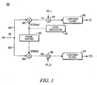
- FIG. 1 shows a known RF direct conversion FM receiver 100 illustrating the problem to be addressed by the present inventions.
- An incoming FM signal x(t) is delivered via an input path 101 having branched connections 103, 105 respectively to two mixers 107, 109.
- a local oscillator 111 generates a reference signal intended to have the same frequency as the carrier frequency of the incoming signal x(t) .
- a first component of the reference signal is applied directly to the mixer 107 where it is multiplied with the input signal x(t) .
- a second component of the reference signal is applied to a phase shifter 113.
- An output of the phase shifter 113 which is the reference signal shifted in phase by ninety degrees is applied to the mixer 109.
- the respective outputs of the mixers 107, 109 are an in-phase component I(t) and a quadrature phase component Q(t) of the input signal x(t).
- the receiver 100 generates a residual DC offset as described earlier and this is shown adding to the components I(t) and Q(t) as components DC_I and DC_Q at junctions 114 and 116 respectively.
- the components I(t) and Q(t) added respectively to the DC offset components DC_I and DC_Q are applied to low pass filters 115 and 117.
- the output signal components from the low pass filters 115 and 117 denoted respectively as I'(t) (I(t) + DC_I) and Q'(t)(Q(t)+DC_Q) are further processed, e.g. in a manner to be described later, to obtain a demodulated signal.
- the branched connections 103, 105 and the components included in them thus form respectively an I-channel and a Q-channel.
- a mathematical analysis of operation of the receiver 100 shown in FIG. 1 is as follows:
- the tone modulation example referred to above assumes use of a signalling tone (audio signal of known frequency carried as a modulation signal) at a frequency ⁇ m that provides frequency modulation in accordance with the industry standard TIA 603.
- TIA 603. This is an industry standard published by TIA and entitled 'Land Mobile FM OR PM Communications Equipment and Performance Standards'.
- the standard includes the following specification details: 'The CDCSS (Continuous Digital Controlled Squelch System) shall define a system where the radio receiver(s) are equipped with tone or data responsive devices that allow audio signals to appear at the receiver audio output, select voice processing such as scrambling, select between voice or data, or control repeater functions, only when a carrier modulated with a specific tone or data pattern is received.
- CDCSS Continuous Digital Controlled Squelch System
- the tone or data pattern must be continuously present for continuous audio output.
- the transmitter emitting the carrier shall be modulated with a continuous tone as in a CTCSS system (Continuous Tone Controlled Squelch System), whose frequency is the same as the tone required to operate the tone-responsive CTCSS device at the receiver output.
- CTCSS system Continuous Tone Controlled Squelch System
- the transmitter emitting the carrier shall in a similar manner be modulated with a continuous NRZ FSK data stream having the correct pattern to operate the data sensitive detector at the receiver output.
- the purpose of the defined system is to minimize the annoyance of hearing communications directed to others sharing the same carrier frequency or channel.
- each user may code his carrier to prevent the reception of audio signals by any uncoded or differently coded carriers
- the CDCSS turn off code is the waveform necessary to disable the audio output of the receiver prior to the RF carrier removal. This serves as a squelch tail or noise eliminator.
- CTCSS/CDCSS and PL/DPL is thus sub-audio signalling under known standard conditions using the protocol of the above TIA standard.
- PL/DPL tones are transmitted in parallel with voice.
- the TIA standard provides a list of suitable tone frequencies, e.g. at 67Hz and 71Hz for PL.
- FIG. 2 shows a RF direct conversion FM receiver 200 embodying the present invention. Components which are the same as in FIG. 1 have the same reference numerals as in FIG. 1 and will not be further described.
- the receiver 200 operates using tone FM modulation as described earlier.
- the local oscillator 111 of FIG. 1 is replaced in the receiver 200 of FIG. 2 by a local oscillator 221 which provides an output reference signal having a frequency which may be shifted by a frequency setter 222 in a manner described later.
- the output signal I'(t) from the low pass filter 115 in the I-channel of the receiver 200 is delivered to a junction 206 and is sampled prior to the junction 206 by a connection 201.
- the connection 201 provides an input connection to an I DC estimator 202 and also to a controller 203 which incorporates a dual purpose offset frequency detector 223.
- the output signal Q'(t) from the low pass filter 117 in the Q-channel is delivered to a junction 207 and is sampled prior to the junction 207 by a connection 204.
- the connection 204 provides an input connection to a Q DC estimator 205 and also to the controller 203.
- An output connection 218 from the controller 203 provides an input connection to the frequency setter 222.
- the I DC estimator 202 estimates, using the sampled input from the connection 201 and also with reference to input signals from the controller 203, a value of DC_I in a manner to be described in detail later and applies at the junction 206 a microvoltage which effectively cancels the estimated DC offset component DC_I.
- the Q DC estimator 205 estimates, using the sampled input from the connection 204 and also with reference to input signals from the controller 203, a value of DC_Q in a manner to be described and applies at the junction 207 a microvoltage which effectively cancels the estimated DC offset component DC_Q.
- the junction 206 provides in a connection 208 of the I-channel a corrected output signal I(t) from which the DC component DC_I has been removed.
- the junction 207 provides in a connection 209 of the Q-channel a corrected output Q(t) from which the DC component DC_Q has been removed.
- These corrected outputs are applied to a processor 210 which calculates a value of the quotient Q(t) / I(t).
- An output signal which represents the quotient value calculated by the processor 210 is passed to a processor 211 which calculates a value of the arctangent of the quotient represented by the signal input to the processor 211.
- An output signal from the processor 211 which represents the calculated arctangent value is passed to a further processor 212 which calculates the differential with respect to time, t, of the input signal to the processor 212 which represents the arctangent value calculated by the processor 211.
- a demodulated output signal is provided by the processor 212 and is provided to an audio output 213 which converts the output signal into an appropriate audio form, e.g. as speech.
- processors include the controller 203, detector 223, frequency setter 222 and the estimators 202 and 205 as well as the processors 210, 211 and 212.
- the modulation 'DC component' J o ( ⁇ ) is now at a frequency f offset Hz offset from DC offset due to hardware to be estimated.
- the integration time (or number of samples for a given sampling frequency) needs to be adaptively controlled as a function of f offset .
- Integration is equivalent to low pass filtering.
- a longer integration time is equivalent to a low pass filter band that is narrower.
- a shorter integration time is equivalent to a low pass filter band that is wider.
- an integration time to be long enough to eliminate the modulation 'DC' component J n ( ⁇ ) which is at a frequency n ⁇ offset .
- I I and Q I are known real sample values stored in a memory incorporated within or associated with the controller 203 and detector 223 for each known received modulating frequency, e.g. for PL or DPL. For example, based on the expected PL/DPL frequency, the values of I I and Q I are stored in the memory.
- Typical bands around offsets of ⁇ m and 2 ⁇ m are indicated by reference indicators B1 and B2 in FIG. 3 .
- the range of each problematic frequency offset in a band around k ⁇ m depends on the integration time operating in the detector 223.
- the problematic frequency range is k ⁇ m ⁇ 20Hz.
- the problematic frequency range is k ⁇ m ⁇ 0.5 Hz .
- the detector 223 determines whether its output is within a problematic frequency band which contains a frequency k n ⁇ m by determining whether the output calculated value of Int is greater than a pre-determined threshold value, THR.
- a preferred inventive procedure 400 (algorithm) which is employed by the controller 203 and detector 223 working in conjunction with the estimators 202 and 205 and the frequency setter 222, in the receiver 200 of FIG. 2 is represented by the flowsheet of FIG. 4 .
- the procedure 400 operates as follows.
- the procedure 400 begins with the receipt of samples of I'(t) and Q'(t) from the I-channel and the Q-channel respectively at a step 401.
- the controller 203 initially sets an integration time of 200 msec for use in the detector 223 and in the estimators 202 and 205.
- the estimators 202 and 205 sample and average I'(t) and Q'(t) in a set of N samples for an integration time, i.e. a sample set time, of 200 msec to obtain values of DC_I_est and DC_Q_est.
- the detector 223 determines whether a calculated value of Int obtained from the detected frequency offset calculation as defined in Equation 10 earlier is greater than the threshold THR shown in FIG. 3 . If the calculated value of Int is not greater than THR, the controller 203 sends a signal to the estimators 202 and 205 to release the DC estimated values, DC_I_est and DC_Q_est, calculated in step 403 for an integration time of 200 msec. So in a step 405 the values of DC_I_est and DC_Q_est are released as outputs from the estimators 202, 205 and are applied as voltage adjustments at the junctions 206, 207. These adjustments are subtracted respectively from I'(t) and Q'(t) in a step 406 to leave only the wanted signals I(t) and Q(t) as outputs in the I-channel and Q-channel respectively in the connections 208, 209.
- step 404 If in step 404 the value of Int calculated by the detector 223 is greater than THR then no signal is issued by the controller 203 to proceed with the calculated values of DC_I_est and DC_Q_est. Instead, in a step 407, the controller 203 checks that the integration time used by the estimators 202, 205 has not yet reached 2000 msec and issues an instruction signal in a step 408 to the estimators 202, 205 to continue their integration (averaging) for another 200 msec. In addition, the detector 223 re-calculates the value of Int in step 403 applied again for another 200 msec - now totally for 400 msec.
- the controller 203 issues a signal in step 405 to the estimators 202, 205 to proceed to release the DC estimated values, DC_I_est and DC_Q_est, that they have calculated with the longer integration time of 400 msec, and these values are subtracted from I'(t) and Q'(t) respectively in step 406.
- step 404 If in step 404 the detected value Int is still greater than THR then no signal is issued by the controller 203 to proceed with the calculated values of DC_I_est and DC_Q_est. Instead, step 407 is re-applied in which the controller 203 checks that the integration time used by the estimators 202, 205 and the detector 223 has not yet reached 2000 msec, and step 408 is re-applied in which the controller issues a signal to the estimators 202, 205 to continue their integration (averaging) for another 200 msec. The detector 223 re-calculates the value of Int in step 403 applied again for another 200 msec - now totally for 600 (200 + 200 + 200) msec.
- the controller 203 issues a signal in step 405 to the estimators 202, 205 to proceed to release the DC estimated values, DC_I_est and DC_Q_est, that they have calculated and these values are subtracted from I'(t) and Q'(t) respectively in step 406.
- steps 407, 408 and 403 are re-applied, and so on.
- Steps 407, 408 and 403 can be successively re-applied causing the integration time to be increased in steps of 200 msec, until a maximum integration time has been reached, e.g. 2000 msec.
- the controller 203 determines in step 407 that the maximum integration time has been reached and a further increase would take the integration time above the maximum, the controller 203 issues a signal in a step 409 via the connection 218 to the frequency setter 222, to shift the frequency of the local oscillator 221 by ⁇ m /2, in practice F PL /2 or F DPL /2 as appropriate.
- the procedure 400 then returns to step 401 and the controller 203 issues a signal for the integration time in the estimators 202, 205 and in the detector 223 to be re-set to 200 msec.
- the method then proceeds again using an integration time of 200 msec in the calculations carried out in step 403 and step 404.
- tone FM modulation has been described in terms of tone FM modulation, the use of tone FM modulation is to be regarded as illustrative rather than limiting.
- the receiver described could also be used to process a signal producing another form of output for a user, e.g. a data output.
- the circuits embodying the invention to compensate for receiver generated DC noise may be used in conjunction with other circuits used for making other corrections.
- the FM receiver e.g. receiver 200
- the FM receiver may include circuit(s) (not shown) to compensate for phase imbalance and/or amplitude imbalance in the I and Q channels, e.g. as described in Applicant's copending UK patent applications GB 0411888.1 and GB 0414459.8 .
Landscapes
- Engineering & Computer Science (AREA)
- Power Engineering (AREA)
- Superheterodyne Receivers (AREA)
- Digital Transmission Methods That Use Modulated Carrier Waves (AREA)
- Noise Elimination (AREA)
Description
- The present invention relates to a receiver for receipt and demodulation of a frequency modulated (FM) signal and a method of operation therein. In particular, the invention relates to a receiver which operates by a direct conversion procedure in which a received FM signal is down-converted directly to a baseband signal.
- Conventional FM receivers have a problem when built using direct conversion architectures. Residual DC offset that is caused by operation of the receiver hardware components adds to the input signal and causes an undesirable distortion in the output, e.g. in the form of an audible signal, provided to a user. The residual DC offset is caused for example by radiation from the local oscillator in the mixers of the receiver, and by DC imbalances in the amplifiers of the receiver.
- In the prior art, the problem has not been dealt with satisfactorily. A one-off correction has been applied, e.g. during factory production. However, the DC offset can vary with time, e.g. as a result of changes in temperature. Thus, the one-off correction can become ineffective with time, particularly if a low tolerance of the DC offset is to be accepted. For example, in some receivers a maximum residual DC offset level of 10µV needs to be achieved whereas the DC offset level present may be as high as 200µV.
-
US6608999 discloses a direct conversion RF receiver. I and Q signals are provided in separate paths. An offset compensation circuit in each path provides a moving average of each signal, which is subtracted from the signal. Once the moving average value has been determined, it is fed back to components located prior to a digital filter in each path, so that each digital filter can be fed with the average value. This allows receiver circuits to be switched off immediately after the average value determination, in order to save power, but without generating noise in the digital filter.US2004/0014450 discloses a direct conversion RF receiver. I and Q signals are provided in separate paths. A compensator compensates for a DC offset in the input signal. - According to the present invention in a first aspect there is provided a receiver for receiving and demodulating a tone frequency modulated RF signal by a direct conversion procedure, the receiver being as defined in
claim 1 of the accompanying claims. - The present invention provides an improved FM receiver in which the problem of undesirable DC offset described above in the receiver is reduced or eliminated. The DC offset may be estimated, in repeated runs of an estimation procedure, by performing a calculation, preferably continuously, by an estimator to estimate the level of DC offset present and by applying a correction using an adjustment signal to cancel the estimated DC offset. Preferably, the calculation and correction are applied using an estimator in each of an I-channel and a Q-channel of the receiver. The calculation performed by the estimator includes (i) taking a set of N samples of the value of an input signal component in the respective channel; (ii) summing the values obtained for the N samples; and (iii) calculating an average value by dividing the sum by the number N of samples.
- Advantageously, the receiver may include a detector which calculates a value of a parameter that is related to a frequency offset between a carrier frequency (centre frequency) of a received FM input signal and a reference frequency of a local oscillator of the receiver. The detector may determine whether the value exceeds a pre-determined threshold. The threshold may indicate that the offset frequency is close to zero or an integral multiple of the frequency of a carried information signal (e.g. an audio or sub-audio signal). The carried signal may beneficially be a known tone frequency as described later. Where the detector determines that the calculated value is greater than the threshold, a controller associated with the detector may increase a sampling (integration) time of the estimator(s) employed to estimate a component of DC offset. Where the sampling time reaches a pre-determined maximum value, the controller may issue a signal which causes the frequency of the reference frequency signal produced by the local oscillator to be shifted by an amount equivalent to half the frequency of an information signal, e.g. audio or sub-audio signal or tone of known frequency, carried by the received input signal.
- The receiver and method according to the invention allow DC receiver offset to be estimated and compensated for frequently or continuously, whilst a FM input signal is being received at the input terminal of the receiver, and without distorting the signal being demodulated, thereby beneficially allowing distortion caused by such DC offset to be suitably minimised or eliminated, thereby improving the quality of a signal provided as an output, e.g. as speech or data information, to a user.
- Embodiments of the present invention will now be described by way of example with reference to the accompanying drawings, in which:
-
-
FIG. 1 is a schematic block circuit diagram of a known FM receiver. -
FIG. 2 is a schematic block circuit diagram of an FM receiver embodying the invention. -
FIG. 3 is a graph of detector output versus offset frequency for a detector employed in the receiver ofFIG. 2 . -
FIG. 4 is a flowsheet illustrating an operational procedure employed in the receiver ofFIG. 2 . -
FIG. 1 shows a known RF directconversion FM receiver 100 illustrating the problem to be addressed by the present inventions. An incoming FM signal x(t) is delivered via aninput path 101 havingbranched connections mixers local oscillator 111 generates a reference signal intended to have the same frequency as the carrier frequency of the incoming signal x(t). A first component of the reference signal is applied directly to themixer 107 where it is multiplied with the input signal x(t). A second component of the reference signal is applied to aphase shifter 113. An output of thephase shifter 113 which is the reference signal shifted in phase by ninety degrees is applied to themixer 109. The respective outputs of themixers receiver 100 generates a residual DC offset as described earlier and this is shown adding to the components I(t) and Q(t) as components DC_I and DC_Q atjunctions low pass filters low pass filters - The
branched connections - A mathematical analysis of operation of the
receiver 100 shown inFIG. 1 is as follows: - The input signal x(t) can be represented in a conventional manner as:

- The output components I'(t) and Q'(t) are as follows:


- For tone FM modulation, explained below, the following simplification can be applied:


- For the I channel with tone FM modulation:

- For the Q channel with tone FM modulation:

- The prior art approach for removing the DC offset in an FM direct conversion receiver is a one-off estimation of the value of the offset and application of an adjustment voltage. However, from the above Equation 4 for the tone FM modulation example, we can see that there is a problem with this approach: removing DC will remove Jo (β) which is a DC component of the modulating information signal and will thereby introduce distortion in an output signal, e.g. an output audio signal such as speech.
- The tone modulation example referred to above assumes use of a signalling tone (audio signal of known frequency carried as a modulation signal) at a frequency ƒm that provides frequency modulation in accordance with the industry standard TIA 603. This is an industry standard published by TIA and entitled 'Land Mobile FM OR PM Communications Equipment and Performance Standards'. The standard includes the following specification details: 'The CDCSS (Continuous Digital Controlled Squelch System) shall define a system where the radio receiver(s) are equipped with tone or data responsive devices that allow audio signals to appear at the receiver audio output, select voice processing such as scrambling, select between voice or data, or control repeater functions, only when a carrier modulated with a specific tone or data pattern is received. The tone or data pattern must be continuously present for continuous audio output. The transmitter emitting the carrier shall be modulated with a continuous tone as in a CTCSS system (Continuous Tone Controlled Squelch System), whose frequency is the same as the tone required to operate the tone-responsive CTCSS device at the receiver output. In a CDCSS system, the transmitter emitting the carrier shall in a similar manner be modulated with a continuous NRZ FSK data stream having the correct pattern to operate the data sensitive detector at the receiver output. The purpose of the defined system is to minimize the annoyance of hearing communications directed to others sharing the same carrier frequency or channel. By using a specific tone or data stream, each user may code his carrier to prevent the reception of audio signals by any uncoded or differently coded carriers The CDCSS turn off code is the waveform necessary to disable the audio output of the receiver prior to the RF carrier removal. This serves as a squelch tail or noise eliminator. To accomplish this, the CDCSS encoder shall transmit a 134.4 +/-0.5 Hz tone for 150 to 200 milliseconds. It can also be a PL/DPL tone. (PL=Private Line, DPL=Digital Private Line)'.
- CTCSS/CDCSS and PL/DPL is thus sub-audio signalling under known standard conditions using the protocol of the above TIA standard. PL/DPL tones are transmitted in parallel with voice. The TIA standard provides a list of suitable tone frequencies, e.g. at 67Hz and 71Hz for PL.
-
FIG. 2 shows a RF directconversion FM receiver 200 embodying the present invention. Components which are the same as inFIG. 1 have the same reference numerals as inFIG. 1 and will not be further described.
Thereceiver 200 operates using tone FM modulation as described earlier. - The
local oscillator 111 ofFIG. 1 is replaced in thereceiver 200 ofFIG. 2 by alocal oscillator 221 which provides an output reference signal having a frequency which may be shifted by afrequency setter 222 in a manner described later. - The output signal I'(t) from the
low pass filter 115 in the I-channel of thereceiver 200 is delivered to ajunction 206 and is sampled prior to thejunction 206 by aconnection 201. Theconnection 201 provides an input connection to anI DC estimator 202 and also to acontroller 203 which incorporates a dual purpose offsetfrequency detector 223. Similarly, the output signal Q'(t) from thelow pass filter 117 in the Q-channel is delivered to ajunction 207 and is sampled prior to thejunction 207 by aconnection 204. Theconnection 204 provides an input connection to aQ DC estimator 205 and also to thecontroller 203. Anoutput connection 218 from thecontroller 203 provides an input connection to thefrequency setter 222. - The I DC estimator 202 estimates, using the sampled input from the
connection 201 and also with reference to input signals from thecontroller 203, a value of DC_I in a manner to be described in detail later and applies at the junction 206 a microvoltage which effectively cancels the estimated DC offset component DC_I. - Similarly, the
Q DC estimator 205 estimates, using the sampled input from theconnection 204 and also with reference to input signals from thecontroller 203, a value of DC_Q in a manner to be described and applies at the junction 207 a microvoltage which effectively cancels the estimated DC offset component DC_Q. - The
junction 206 provides in aconnection 208 of the I-channel a corrected output signal I(t) from which the DC component DC_I has been removed. Likewise, thejunction 207 provides in a connection 209 of the Q-channel a corrected output Q(t) from which the DC component DC_Q has been removed. These corrected outputs are applied to aprocessor 210 which calculates a value of the quotient Q(t)/I(t). An output signal which represents the quotient value calculated by theprocessor 210 is passed to aprocessor 211 which calculates a value of the arctangent of the quotient represented by the signal input to theprocessor 211. An output signal from theprocessor 211 which represents the calculated arctangent value is passed to afurther processor 212 which calculates the differential with respect to time, t, of the input signal to theprocessor 212 which represents the arctangent value calculated by theprocessor 211. Finally, a demodulated output signal is provided by theprocessor 212 and is provided to anaudio output 213 which converts the output signal into an appropriate audio form, e.g. as speech. - It will be apparent to those skilled in the art that in practice a single processor device, e.g. in the form of a programmed digital signal microprocessor, may perform the functions of any two or more of the processors employed in the
receiver 200 shown inFIG. 2 , Such processors include thecontroller 203,detector 223,frequency setter 222 and theestimators processors - Operation of the
controller 203, thedetector 223 and theestimators - Let us examine the equation for the signal I'(t):

receiver 200 is tuned (by providing a reference signal of suitable frequency by the local oscillator 221) to exactly the same frequency as the transmitter carrier frequency, i.e. there is no frequency error. In practice, there is always likely to be some finite frequency offset between the carrier frequency of the received FM signal and the frequency of the reference signal produced by thelocal oscillator 221. This offset can be as small as 0.1 Hz or as large as 500 Hz. We shall assume that there is frequency offset of ƒoffset Hz. For a low RF input signal (-120 to -90 dBm) the DC offset due to receiver hardware is higher than the DC component due to modulation Jo (β). So at low RF signal levels the DC offset due to hardware is more dominant in the form of undesired audio distortion. - In order to estimate accurately the DC offset component due to receiver hardware with a target accuracy of 10 µV we need the modulation DC component Jo (β) to be less then 1 µV. For -60 dBm at the antenna the DC component due to modulation is 10000 uV (worst case example). So an attenuation of 80 dB is needed for this example. Then the expression for I'(t) will be:

- With a frequency offset present the modulation 'DC component' Jo(β) is now at a frequency foffset Hz offset from DC offset due to hardware to be estimated.
Estimation of the DC offset components due to hardware may be done by integrating or summing the values of I'(t) and Q'(t) obtained in a set of N discrete samples over a suitable integration or summing period and then calculating an average by dividing the sum obtained by dividing by the number N of samples. From the expression for I'(t) in Equation 7 above, we can see that if ƒ offset = 0 then Jo (β) appears at zero frequency. If foffset = n·ƒPL , where n is a positive or negative integer, and ƒPL is used as ƒm , then the Bessel component Jn (β) will also appear at zero frequency. So if we integrate I'(t) over a long enough period and if Jn (β) is not at zero frequency offset, we will obtain only the required DC component at 0 Hz, namely the DC offset component due to hardware, DC_I(t). - However, in order to produce a correct DC estimation that will only include the component DC_I(t) the integration time (or number of samples for a given sampling frequency) needs to be adaptively controlled as a function of foffset. This can be explained as follows. Integration is equivalent to low pass filtering. A longer integration time is equivalent to a low pass filter band that is narrower. A shorter integration time is equivalent to a low pass filter band that is wider. In our case we need an integration time to be long enough to eliminate the modulation 'DC' component Jn (β) which is at a frequency nƒoffset.
- This integration procedure to produce an estimated value of DC_I(t), namely DC_I(t)_est, and of DC_Q(t), namely DC_Q(t)_est, can be summarized by the following equations:


T int is the integration or averaging time and will be inversely proportional to the frequency offset foffset , N int is the number of samples taken per set and ƒsampling is the sampling frequency. Thecontroller 203 inFIG. 2 using calculations carried out by thedetector 223 adaptively sets the integration time T int as explained later. If increasing the integration time does not help, the reference frequency produced by thelocal oscillator 111 will be shifted. The integration time should follow the following rule: ƒPL·Tint = M or ƒDPL ·Tint = M, where M is an integer, ƒPL is the PL frequency and ƒDPL is the DPL frequency for tone FM modulation as defined earlier. This is so that the integration time is an integer multiple of the FM tone frequency, using PL or DPL. - The
detector 223 which is incorporated in thecontroller 203 calculates a value of a parameter which is related to (an inverse function of) the offset frequency present between the received carrier signal and the reference signal produced by thelocal oscillator 221. If thedetector 223 detects an offset frequency ƒoffset =k·ƒm, where k is zero or an integer, thecontroller 203 will issue a signal which will disable application of the correction estimated by theestimators - Operation of the dual purpose offset
frequency detector 203 is based on a modified correlation by operation of the following relationship (Equation 10):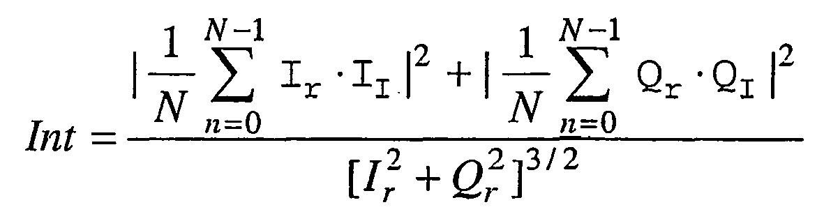
where II = sin(β·sin(2·π·ƒpl ·t))
QI = cos(β·sin(2·π·ƒpl·t))
Normalization by
detector 223 will provide a higher output for a low RF input signal. Ir and Qr are received signals. II and QI are known real sample values stored in a memory incorporated within or associated with thecontroller 203 anddetector 223 for each known received modulating frequency, e.g. for PL or DPL. For example, based on the expected PL/DPL frequency, the values of II and QI are stored in the memory. - The output of the
detector 223, which is the value of the parameter Int defined in Equation 10, as a function of offset frequency (Δf) for a received FM signal having a modulating signal frequency ƒm , e.g. a PL or DPL tone, has a form shown inFIG. 3 . Bands are obtained around offsets of kƒm , where k=0 or an integer. Typical bands around offsets of ƒm and 2ƒm , are indicated by reference indicators B1 and B2 inFIG. 3 . The range of each problematic frequency offset in a band around kƒ m depends on the integration time operating in thedetector 223. For example, for an integration time of 150 msec the problematic frequency range is kƒm ±20Hz. For an integration time of 2000 msec the problematic frequency range is kƒm ±0.5Hz. Thedetector 223 determines whether its output is within a problematic frequency band which contains a frequency knƒm by determining whether the output calculated value of Int is greater than a pre-determined threshold value, THR. - A preferred inventive procedure 400 (algorithm) which is employed by the
controller 203 anddetector 223 working in conjunction with theestimators frequency setter 222, in thereceiver 200 ofFIG. 2 is represented by the flowsheet ofFIG. 4 . Theprocedure 400 operates as follows. - The
procedure 400 begins with the receipt of samples of I'(t) and Q'(t) from the I-channel and the Q-channel respectively at astep 401. In astep 402, thecontroller 203 initially sets an integration time of 200 msec for use in thedetector 223 and in theestimators step 403, theestimators step 404, thedetector 223 determines whether a calculated value of Int obtained from the detected frequency offset calculation as defined in Equation 10 earlier is greater than the threshold THR shown inFIG. 3 . If the calculated value of Int is not greater than THR, thecontroller 203 sends a signal to theestimators step 403 for an integration time of 200 msec. So in astep 405 the values of DC_I_est and DC_Q_est are released as outputs from theestimators junctions step 406 to leave only the wanted signals I(t) and Q(t) as outputs in the I-channel and Q-channel respectively in theconnections 208, 209. - If in
step 404 the value of Int calculated by thedetector 223 is greater than THR then no signal is issued by thecontroller 203 to proceed with the calculated values of DC_I_est and DC_Q_est. Instead, in astep 407, thecontroller 203 checks that the integration time used by theestimators step 408 to theestimators detector 223 re-calculates the value of Int instep 403 applied again for another 200 msec - now totally for 400 msec. If, after those total 400 (200+200) msec, the value of Int is now less than THR, thecontroller 203 issues a signal instep 405 to theestimators step 406. - If in
step 404 the detected value Int is still greater than THR then no signal is issued by thecontroller 203 to proceed with the calculated values of DC_I_est and DC_Q_est. Instead, step 407 is re-applied in which thecontroller 203 checks that the integration time used by theestimators detector 223 has not yet reached 2000 msec, and step 408 is re-applied in which the controller issues a signal to theestimators detector 223 re-calculates the value of Int instep 403 applied again for another 200 msec - now totally for 600 (200 + 200 + 200) msec. If, after that total period of 600 msec, the value of Int is now less than THR, thecontroller 203 issues a signal instep 405 to theestimators step 406. However, if after that period of 600 msec the values of Int is still greater than THR, then steps 407, 408 and 403 are re-applied, and so on. -
Steps controller 203 determines instep 407 that the maximum integration time has been reached and a further increase would take the integration time above the maximum, thecontroller 203 issues a signal in astep 409 via theconnection 218 to thefrequency setter 222, to shift the frequency of thelocal oscillator 221 by ƒm /2, in practice FPL/2 or FDPL/2 as appropriate. Theprocedure 400 then returns to step 401 and thecontroller 203 issues a signal for the integration time in theestimators detector 223 to be re-set to 200 msec. The method then proceeds again using an integration time of 200 msec in the calculations carried out instep 403 andstep 404. - Although the embodiments of the invention above have been described in terms of tone FM modulation, the use of tone FM modulation is to be regarded as illustrative rather than limiting.
- Also, although the above embodiments have been described in terms of processing a signal to produce an audio output, the receiver described could also be used to process a signal producing another form of output for a user, e.g. a data output.
- The circuits embodying the invention to compensate for receiver generated DC noise may be used in conjunction with other circuits used for making other corrections. For example, the FM receiver (e.g. receiver 200) may include circuit(s) (not shown) to compensate for phase imbalance and/or amplitude imbalance in the I and Q channels, e.g. as described in Applicant's copending UK patent applications
GB 0411888.1 GB 0414459.8
Claims (11)
- A receiver (200) for receiving and demodulating a tone frequency modulated RF signal by a direct conversion procedure including an input signal path (101) for receiving an RF input signal and, connected to the input signal path, component channels (103, 105) for processing in-phase (1) and quadrature phase (Q) components of the input signal;
wherein the receiver (200) further includes a compensator coupled to one of the component channels (103, 105) and configured to measure and compensate for DC offset produced by the receiver hardware and combined with an input signal component in the respective channel, the compensator including:an estimator (202, 205) operable to estimate a receiver hardware induced component of DC offset present in the one of the component channels (103, 105) by using an integration procedure calculated over an integration time period; andan estimator controller (203) operably coupled to the estimator (202, 205) and operable to:(i) calculate a first parameter, via an offset frequency detector (223) portion of the estimator controller (203), as an inverse function of a determined offset frequency present between a carrier frequency of the RF input signal and a locally generated reference signal;(ii) compare (404) the first parameter to a threshold value,(iii) if the first parameter is equal to or less than the threshold value, control (406) the estimator (202, 205) to compensate for the receiver hardware induced component of DC offset estimated over the integration time period; and(iv) if the first parameter is greater than the threshold value, control the estimator (202, 205) to temporarily suspend compensation for the receiver hardware induced component of DC offset, and instead re-estimate the receiver hardware induced component of DC offset using a second integration time period longer than the integration time period. - A receiver (200) according to claim 1, wherein the estimator (202, 205) is operable to estimate the receiver hardware induced component of the DC offset present in the one of the component channels by:(i) taking a set ofN samples of the value of the input signal component in the one of the component channels;(ii) summing the values obtained for the N samples; and(iii) calculating an average value by dividing the sum by the number N of samples, and wherein the receiver (200) further comprises a combiner operable to combine with the input signal component an adjustment signal which cancels the receiver hardware induced component of the DC offset present in the one of the component channels.
- A receiver (200) according to claim 1 or claim 2, further comprising:an I-channel (103) connected to the input signal path (101) including a first mixer (107) for mixing the RF input signal with an in-phase reference signal to produce an in-phase component (I(t)) of the input signal in an I-channel;a Q-channel (105) connected to the input signal path (101) including a second mixer (109) for mixing the input signal with a quadrature-phase reference signal to produce a quadrature-phase component (Q(t)) of the input signal in the Q-channel;an I-channel compensator for measuring and compensating for a receiver hardware induced component of DC offset present in the I-channel combined with the input signal component in the I-channel; anda Q-channel compensator for measuring and compensating for a receiver hardware induced component of DC offset present in the Q-channel combined with the input signal component in the Q-channel.
- A receiver (200) according to claim 3, wherein the I-channel compensator and the Q-channel compensator each include estimators (202, 205) which are operable to take a same number N of samples of the input signal components, in a given set of samples.
- A receiver (200) according to claim 4, wherein the estimator (202, 205) of at least one of the I-channel compensator and the Q-channel compensator is operable to take a number N of samples in a set of samples which is variable from set-to-set.
- A receiver (200) according to any previous claim, wherein:the estimator controller (203) is operable to control (408) the integration time period used by the estimator (202, 205) to sample a set of values of the one of the component channels (103, 105); andwherein the offset frequency detector (223) is operable, where an offset frequency is determined to be within a band which includes a frequency k. fm, where k is zero or an integer and fm is a modulating frequency of the input signal, to cause the estimator to issue a signal to suspend compensation for the receiver hardware induced component of DC offset, and instead re-estimate the receiver hardware induced component of DC offset using the second integration time period longer than the integration time period.
- A receiver (200) according to claim 6, wherein
a value of the first parameter Int is given by:
where II = sin(β·sin(2·π·ƒm·t)) and
QI = cos(β·sin(2·π·ƒm·t)),
where Ir and Qr are received FM modulated signal quadrature components, and
where II and QI are component values stored in a memory associated with the detector, for a given received signal having a modulating frequency ƒm and a modulation index β. - A receiver (200) according to claim 7, wherein the estimator controller (203) is operable, if the first parameter is greater than the threshold value, to re-calculate the first parameter value after the increased integration time.
- A receiver (200) according to claim 3, further comprising:a local oscillator (221) for producing the reference signal and a phase shifter (113) connected to the local oscillator (221) for shifting phase of the reference signal to produce the quadrature phase reference signal and a frequency setter (222) for setting the frequency of the reference signal produced by the local oscillator (221), the frequency setter (222) being operable to vary the frequency of the reference signal; andthe estimator controller (203) operably coupled to the frequency setter (222), the offset detector operable to calculate the first parameter as an inverse function of a determined offset frequency present between the carrier frequency of the RF input signal and the reference signal and, where an offset frequency is determined to be within a band which includes a frequency k. fm where k is zero or an integer, and fm is a modulating frequency of the input signal, and the estimator controller (203) is operable to issue a signal to the frequency setter to shift the reference frequency to a frequency outside the band.
- A receiver (200) according to claim 9, wherein:a value of the first parameter Int is given by:the frequency setter (222) is operable, in response to receipt of a signal from the estimator controller (203), to change the in-phase reference frequency by an amount which is substantially equal to one half of the value of the frequency ƒm ; and

where II = sin(β·sin(2·π·ƒm ·t)) and
QI = cos(β·sin(2·π·ƒm·t)),
where Ir and Qr are received FM modulated signal quadrature components, and
where II and QI are component values stored in a memory associated with the offset detector for a given received signal having a modulating frequency ƒm and modulation index β;
the estimator controller (203) is operable to issue (409) a signal to the frequency setter (222) to change the in-phase reference frequency when a further integration time used by the offset detector has reached a pre-determined maximum value. - A receiver (200) according to claim 1, wherein the estimator controller (203) is operable to iteratively, over longer and longer integration time periods, temporarily suspend compensation for the receiver hardware induced component of DC offset and instead re-estimate the receiver hardware induced component of DC offset using the longer and longer integration time periods, until either it is determined that the re-calculated first parameter is equal to or less than the threshold value or it is determined (407) that a predetermined maximum integration value is reached, after which time the estimator controller (203) controls the estimator (202, 205) to compensate for the receiver hardware induced component of DC offset estimated over the predetermined maximum integration time period.
Applications Claiming Priority (2)
| Application Number | Priority Date | Filing Date | Title |
|---|---|---|---|
| GB0505493A GB2424326B (en) | 2005-03-18 | 2005-03-18 | Receiver for receipt and demodulation of a frequency modulated RF signal and method of operation therein |
| PCT/US2006/006821 WO2006101672A1 (en) | 2005-03-18 | 2006-02-27 | Receiver for receipt and demodulation of a frequency modulated rf signal and method of operation therein |
Publications (3)
| Publication Number | Publication Date |
|---|---|
| EP1869779A1 EP1869779A1 (en) | 2007-12-26 |
| EP1869779A4 EP1869779A4 (en) | 2009-07-22 |
| EP1869779B1 true EP1869779B1 (en) | 2013-04-10 |
Family
ID=34509231
Family Applications (1)
| Application Number | Title | Priority Date | Filing Date |
|---|---|---|---|
| EP06736197.2A Expired - Lifetime EP1869779B1 (en) | 2005-03-18 | 2006-02-27 | Receiver for receipt and demodulation of a frequency modulated rf signal and method of operation therein |
Country Status (5)
| Country | Link |
|---|---|
| EP (1) | EP1869779B1 (en) |
| JP (1) | JP4663009B2 (en) |
| CN (1) | CN101142751B (en) |
| GB (1) | GB2424326B (en) |
| WO (1) | WO2006101672A1 (en) |
Families Citing this family (8)
| Publication number | Priority date | Publication date | Assignee | Title |
|---|---|---|---|---|
| CN101478317B (en) * | 2008-12-25 | 2012-02-01 | 苏州全波通信技术有限公司 | IQ amplitude adaptive balance system in direct frequency conversion modulation |
| JP4830012B2 (en) * | 2009-09-01 | 2011-12-07 | シャープ株式会社 | Front-end circuit, tuner and TV broadcast receiver |
| EP2373009A3 (en) * | 2010-03-31 | 2014-05-28 | Sony Corporation | Television signal receiver apparatus with sound signal detection |
| US8358164B2 (en) * | 2010-11-30 | 2013-01-22 | Infineon Technologies Ag | Square wave signal component cancellation |
| JP5599352B2 (en) * | 2011-03-30 | 2014-10-01 | パナソニック株式会社 | Receiver |
| US9455853B2 (en) * | 2014-12-30 | 2016-09-27 | Stmicroelectronics, Inc. | Device and method for FM demodulation with threshold extension |
| JP6341105B2 (en) * | 2015-01-26 | 2018-06-13 | 株式会社Jvcケンウッド | FM receiver and FM receiving method |
| GB201907717D0 (en) | 2019-05-31 | 2019-07-17 | Nordic Semiconductor Asa | Apparatus and methods for dc-offset estimation |
Family Cites Families (18)
| Publication number | Priority date | Publication date | Assignee | Title |
|---|---|---|---|---|
| JP2687851B2 (en) * | 1992-10-19 | 1997-12-08 | 日本電気株式会社 | Receiving machine |
| EP0594894B1 (en) * | 1992-10-28 | 1999-03-31 | Alcatel | DC offset correction for direct-conversion TDMA receiver |
| KR100355684B1 (en) * | 1992-11-26 | 2002-12-11 | 코닌클리케 필립스 일렉트로닉스 엔.브이. | Direct conversion receiver |
| TW225067B (en) * | 1992-11-26 | 1994-06-11 | Philips Electronics Nv | |
| JPH06188637A (en) * | 1992-12-17 | 1994-07-08 | Fujitsu Ten Ltd | Direct conversion reception circuit |
| US5422880A (en) * | 1993-04-05 | 1995-06-06 | Stratacom, Inc. | Broadband switching fabric in a communication controller |
| FI94818C (en) * | 1993-06-02 | 1995-10-25 | Nokia Telecommunications Oy | A method for demodulating a digitally modulated signal and a demodulator |
| GB2283871B (en) * | 1993-10-28 | 1998-01-21 | Plessey Semiconductors Ltd | Control arrangements for digital radio receivers |
| JPH09224059A (en) * | 1996-02-15 | 1997-08-26 | General Res Of Electron Inc | Direct conversion fsk receiver |
| JP3731276B2 (en) * | 1997-03-03 | 2006-01-05 | 三菱電機株式会社 | Receiving machine |
| SE513332C2 (en) | 1998-11-26 | 2000-08-28 | Ericsson Telefon Ab L M | Communication signal receiver and operating method for the same |
| GB2349313A (en) * | 1999-04-21 | 2000-10-25 | Ericsson Telefon Ab L M | Radio receiver |
| JP2002135347A (en) * | 2000-10-24 | 2002-05-10 | Sony Corp | Direct conversion receiver |
| US7522900B2 (en) * | 2001-03-20 | 2009-04-21 | Broadcom Corporation | DC offset correction for use in a radio architecture |
| JP3833924B2 (en) * | 2001-10-26 | 2006-10-18 | 株式会社日立国際電気 | Direct conversion receiver |
| US7212797B2 (en) * | 2002-04-26 | 2007-05-01 | Qualcomm Incorporated | DC removal techniques for wireless networking |
| JP2004048581A (en) | 2002-07-15 | 2004-02-12 | Hitachi Ltd | Receiver and gain control system |
| JP3906179B2 (en) * | 2003-04-25 | 2007-04-18 | 株式会社東芝 | Radio receiver and radio signal processing method |
-
2005
- 2005-03-18 GB GB0505493A patent/GB2424326B/en not_active Expired - Fee Related
-
2006
- 2006-02-27 EP EP06736197.2A patent/EP1869779B1/en not_active Expired - Lifetime
- 2006-02-27 CN CN200680008650.4A patent/CN101142751B/en not_active Expired - Fee Related
- 2006-02-27 JP JP2008501898A patent/JP4663009B2/en not_active Expired - Fee Related
- 2006-02-27 WO PCT/US2006/006821 patent/WO2006101672A1/en not_active Ceased
Also Published As
| Publication number | Publication date |
|---|---|
| CN101142751B (en) | 2015-11-25 |
| GB2424326A (en) | 2006-09-20 |
| CN101142751A (en) | 2008-03-12 |
| GB0505493D0 (en) | 2005-04-20 |
| JP2008536367A (en) | 2008-09-04 |
| EP1869779A1 (en) | 2007-12-26 |
| GB2424326B (en) | 2008-01-16 |
| WO2006101672A1 (en) | 2006-09-28 |
| JP4663009B2 (en) | 2011-03-30 |
| EP1869779A4 (en) | 2009-07-22 |
Similar Documents
| Publication | Publication Date | Title |
|---|---|---|
| US6498929B1 (en) | Receiver having DC offset decreasing function and communication system using the same | |
| RU2146416C1 (en) | Direct-detection digital-correction receiver | |
| JP4718075B2 (en) | Apparatus and method for compensating for interference of direct conversion transceiver | |
| US6950480B2 (en) | Receiver having automatic burst mode I/Q gain and phase balance | |
| US20060068739A1 (en) | Receiver, receiving method and portable wireless apparatus | |
| JP2607847Y2 (en) | Receiver including frequency deviation evaluator | |
| US20070229340A1 (en) | Automatic gain control | |
| JPH1056394A (en) | D. in direct conversion receiver C. Offset removal and spurious AM suppression method and apparatus | |
| KR20010071126A (en) | Distortion correction circuit for direct conversion receiver | |
| EP1222743B1 (en) | Receiver, transceiver, radio unit and method for telecommunication | |
| US7769358B2 (en) | Radio system, radio transmitter, and radio receiver | |
| US7248654B2 (en) | Apparatus and method for compensating I/Q imbalance based on gain-controlled reference channel in orthogonal frequency division multiplex | |
| JP5935631B2 (en) | Compensation device and wireless communication device | |
| WO2011086640A1 (en) | Transmitter apparatus, wireless communication apparatus and transmission method | |
| EP1147615B1 (en) | A homodyne radio receiver | |
| CN101142751B (en) | Receiver for receiving and demodulating frequency modulated RF signals and method of operation therein | |
| JP2001024619A (en) | OFDM signal receiver | |
| KR100251586B1 (en) | Automatic Gain Control of Received Signal in Digital Mobile Communication System | |
| WO2005093979A1 (en) | Radio system and radio communication device | |
| AU2005251078B2 (en) | Receiver and method for wireless communications terminal | |
| JP3678896B2 (en) | Automatic frequency control method | |
| JP3436250B2 (en) | Transmission device | |
| CN100527644C (en) | Radio system, radio transmitter, and radio receiver | |
| KR102064038B1 (en) | Adaptive Phase Adjustor and method to remove the effect of multi-path fading | |
| KR19980080175A (en) | Apparatus and Suppression Method for Suppressing Interference DC Component Shift in a Direct Conversion Wireless Receiver |
Legal Events
| Date | Code | Title | Description |
|---|---|---|---|
| PUAI | Public reference made under article 153(3) epc to a published international application that has entered the european phase |
Free format text: ORIGINAL CODE: 0009012 |
|
| 17P | Request for examination filed |
Effective date: 20071018 |
|
| AK | Designated contracting states |
Kind code of ref document: A1 Designated state(s): AT BE BG CH CY CZ DE DK EE ES FI FR GB GR HU IE IS IT LI LT LU LV MC NL PL PT RO SE SI SK TR |
|
| DAX | Request for extension of the european patent (deleted) | ||
| A4 | Supplementary search report drawn up and despatched |
Effective date: 20090622 |
|
| RAP1 | Party data changed (applicant data changed or rights of an application transferred) |
Owner name: MOTOROLA SOLUTIONS, INC. |
|
| 17Q | First examination report despatched |
Effective date: 20120215 |
|
| GRAP | Despatch of communication of intention to grant a patent |
Free format text: ORIGINAL CODE: EPIDOSNIGR1 |
|
| GRAS | Grant fee paid |
Free format text: ORIGINAL CODE: EPIDOSNIGR3 |
|
| GRAA | (expected) grant |
Free format text: ORIGINAL CODE: 0009210 |
|
| AK | Designated contracting states |
Kind code of ref document: B1 Designated state(s): AT BE BG CH CY CZ DE DK EE ES FI FR GB GR HU IE IS IT LI LT LU LV MC NL PL PT RO SE SI SK TR |
|
| REG | Reference to a national code |
Ref country code: GB Ref legal event code: FG4D Ref country code: DE Ref legal event code: R081 Ref document number: 602006035571 Country of ref document: DE Owner name: MOTOROLA SOLUTIONS, INC., CHICAGO, US Free format text: FORMER OWNER: MOTOROLA, INC., SCHAUMBURG, ILL., US |
|
| REG | Reference to a national code |
Ref country code: CH Ref legal event code: EP Ref country code: AT Ref legal event code: REF Ref document number: 606486 Country of ref document: AT Kind code of ref document: T Effective date: 20130415 |
|
| REG | Reference to a national code |
Ref country code: IE Ref legal event code: FG4D |
|
| REG | Reference to a national code |
Ref country code: DE Ref legal event code: R096 Ref document number: 602006035571 Country of ref document: DE Effective date: 20130606 |
|
| PG25 | Lapsed in a contracting state [announced via postgrant information from national office to epo] |
Ref country code: SI Free format text: LAPSE BECAUSE OF FAILURE TO SUBMIT A TRANSLATION OF THE DESCRIPTION OR TO PAY THE FEE WITHIN THE PRESCRIBED TIME-LIMIT Effective date: 20130410 |
|
| REG | Reference to a national code |
Ref country code: AT Ref legal event code: MK05 Ref document number: 606486 Country of ref document: AT Kind code of ref document: T Effective date: 20130410 |
|
| REG | Reference to a national code |
Ref country code: LT Ref legal event code: MG4D Ref country code: NL Ref legal event code: VDEP Effective date: 20130410 |
|
| PG25 | Lapsed in a contracting state [announced via postgrant information from national office to epo] |
Ref country code: BE Free format text: LAPSE BECAUSE OF FAILURE TO SUBMIT A TRANSLATION OF THE DESCRIPTION OR TO PAY THE FEE WITHIN THE PRESCRIBED TIME-LIMIT Effective date: 20130410 Ref country code: NL Free format text: LAPSE BECAUSE OF FAILURE TO SUBMIT A TRANSLATION OF THE DESCRIPTION OR TO PAY THE FEE WITHIN THE PRESCRIBED TIME-LIMIT Effective date: 20130410 Ref country code: LT Free format text: LAPSE BECAUSE OF FAILURE TO SUBMIT A TRANSLATION OF THE DESCRIPTION OR TO PAY THE FEE WITHIN THE PRESCRIBED TIME-LIMIT Effective date: 20130410 Ref country code: AT Free format text: LAPSE BECAUSE OF FAILURE TO SUBMIT A TRANSLATION OF THE DESCRIPTION OR TO PAY THE FEE WITHIN THE PRESCRIBED TIME-LIMIT Effective date: 20130410 Ref country code: IS Free format text: LAPSE BECAUSE OF FAILURE TO SUBMIT A TRANSLATION OF THE DESCRIPTION OR TO PAY THE FEE WITHIN THE PRESCRIBED TIME-LIMIT Effective date: 20130810 Ref country code: ES Free format text: LAPSE BECAUSE OF FAILURE TO SUBMIT A TRANSLATION OF THE DESCRIPTION OR TO PAY THE FEE WITHIN THE PRESCRIBED TIME-LIMIT Effective date: 20130721 Ref country code: PT Free format text: LAPSE BECAUSE OF FAILURE TO SUBMIT A TRANSLATION OF THE DESCRIPTION OR TO PAY THE FEE WITHIN THE PRESCRIBED TIME-LIMIT Effective date: 20130812 Ref country code: FI Free format text: LAPSE BECAUSE OF FAILURE TO SUBMIT A TRANSLATION OF THE DESCRIPTION OR TO PAY THE FEE WITHIN THE PRESCRIBED TIME-LIMIT Effective date: 20130410 Ref country code: GR Free format text: LAPSE BECAUSE OF FAILURE TO SUBMIT A TRANSLATION OF THE DESCRIPTION OR TO PAY THE FEE WITHIN THE PRESCRIBED TIME-LIMIT Effective date: 20130711 Ref country code: SE Free format text: LAPSE BECAUSE OF FAILURE TO SUBMIT A TRANSLATION OF THE DESCRIPTION OR TO PAY THE FEE WITHIN THE PRESCRIBED TIME-LIMIT Effective date: 20130410 |
|
| PG25 | Lapsed in a contracting state [announced via postgrant information from national office to epo] |
Ref country code: CY Free format text: LAPSE BECAUSE OF FAILURE TO SUBMIT A TRANSLATION OF THE DESCRIPTION OR TO PAY THE FEE WITHIN THE PRESCRIBED TIME-LIMIT Effective date: 20130410 Ref country code: BG Free format text: LAPSE BECAUSE OF FAILURE TO SUBMIT A TRANSLATION OF THE DESCRIPTION OR TO PAY THE FEE WITHIN THE PRESCRIBED TIME-LIMIT Effective date: 20130710 Ref country code: PL Free format text: LAPSE BECAUSE OF FAILURE TO SUBMIT A TRANSLATION OF THE DESCRIPTION OR TO PAY THE FEE WITHIN THE PRESCRIBED TIME-LIMIT Effective date: 20130410 Ref country code: LV Free format text: LAPSE BECAUSE OF FAILURE TO SUBMIT A TRANSLATION OF THE DESCRIPTION OR TO PAY THE FEE WITHIN THE PRESCRIBED TIME-LIMIT Effective date: 20130410 |
|
| PG25 | Lapsed in a contracting state [announced via postgrant information from national office to epo] |
Ref country code: DK Free format text: LAPSE BECAUSE OF FAILURE TO SUBMIT A TRANSLATION OF THE DESCRIPTION OR TO PAY THE FEE WITHIN THE PRESCRIBED TIME-LIMIT Effective date: 20130410 Ref country code: SK Free format text: LAPSE BECAUSE OF FAILURE TO SUBMIT A TRANSLATION OF THE DESCRIPTION OR TO PAY THE FEE WITHIN THE PRESCRIBED TIME-LIMIT Effective date: 20130410 Ref country code: EE Free format text: LAPSE BECAUSE OF FAILURE TO SUBMIT A TRANSLATION OF THE DESCRIPTION OR TO PAY THE FEE WITHIN THE PRESCRIBED TIME-LIMIT Effective date: 20130410 Ref country code: CZ Free format text: LAPSE BECAUSE OF FAILURE TO SUBMIT A TRANSLATION OF THE DESCRIPTION OR TO PAY THE FEE WITHIN THE PRESCRIBED TIME-LIMIT Effective date: 20130410 |
|
| PLBE | No opposition filed within time limit |
Free format text: ORIGINAL CODE: 0009261 |
|
| STAA | Information on the status of an ep patent application or granted ep patent |
Free format text: STATUS: NO OPPOSITION FILED WITHIN TIME LIMIT |
|
| PG25 | Lapsed in a contracting state [announced via postgrant information from national office to epo] |
Ref country code: IT Free format text: LAPSE BECAUSE OF FAILURE TO SUBMIT A TRANSLATION OF THE DESCRIPTION OR TO PAY THE FEE WITHIN THE PRESCRIBED TIME-LIMIT Effective date: 20130410 Ref country code: RO Free format text: LAPSE BECAUSE OF FAILURE TO SUBMIT A TRANSLATION OF THE DESCRIPTION OR TO PAY THE FEE WITHIN THE PRESCRIBED TIME-LIMIT Effective date: 20130410 |
|
| 26N | No opposition filed |
Effective date: 20140113 |
|
| REG | Reference to a national code |
Ref country code: DE Ref legal event code: R097 Ref document number: 602006035571 Country of ref document: DE Effective date: 20140113 |
|
| PG25 | Lapsed in a contracting state [announced via postgrant information from national office to epo] |
Ref country code: LU Free format text: LAPSE BECAUSE OF FAILURE TO SUBMIT A TRANSLATION OF THE DESCRIPTION OR TO PAY THE FEE WITHIN THE PRESCRIBED TIME-LIMIT Effective date: 20140227 Ref country code: MC Free format text: LAPSE BECAUSE OF FAILURE TO SUBMIT A TRANSLATION OF THE DESCRIPTION OR TO PAY THE FEE WITHIN THE PRESCRIBED TIME-LIMIT Effective date: 20130410 |
|
| REG | Reference to a national code |
Ref country code: CH Ref legal event code: PL |
|
| PG25 | Lapsed in a contracting state [announced via postgrant information from national office to epo] |
Ref country code: CH Free format text: LAPSE BECAUSE OF NON-PAYMENT OF DUE FEES Effective date: 20140228 Ref country code: LI Free format text: LAPSE BECAUSE OF NON-PAYMENT OF DUE FEES Effective date: 20140228 |
|
| REG | Reference to a national code |
Ref country code: FR Ref legal event code: ST Effective date: 20141031 |
|
| REG | Reference to a national code |
Ref country code: IE Ref legal event code: MM4A |
|
| PG25 | Lapsed in a contracting state [announced via postgrant information from national office to epo] |
Ref country code: FR Free format text: LAPSE BECAUSE OF NON-PAYMENT OF DUE FEES Effective date: 20140228 Ref country code: IE Free format text: LAPSE BECAUSE OF NON-PAYMENT OF DUE FEES Effective date: 20140227 |
|
| PG25 | Lapsed in a contracting state [announced via postgrant information from national office to epo] |
Ref country code: TR Free format text: LAPSE BECAUSE OF FAILURE TO SUBMIT A TRANSLATION OF THE DESCRIPTION OR TO PAY THE FEE WITHIN THE PRESCRIBED TIME-LIMIT Effective date: 20130410 Ref country code: HU Free format text: LAPSE BECAUSE OF FAILURE TO SUBMIT A TRANSLATION OF THE DESCRIPTION OR TO PAY THE FEE WITHIN THE PRESCRIBED TIME-LIMIT; INVALID AB INITIO Effective date: 20060227 |
|
| REG | Reference to a national code |
Ref country code: DE Ref legal event code: R082 Ref document number: 602006035571 Country of ref document: DE Representative=s name: SCHUMACHER & WILLSAU PATENTANWALTSGESELLSCHAFT, DE Ref country code: DE Ref legal event code: R081 Ref document number: 602006035571 Country of ref document: DE Owner name: MOTOROLA SOLUTIONS, INC., CHICAGO, US Free format text: FORMER OWNER: MOTOROLA SOLUTIONS, INC., SCHAUMBURG, ILL., US |
|
| PGFP | Annual fee paid to national office [announced via postgrant information from national office to epo] |
Ref country code: GB Payment date: 20230214 Year of fee payment: 18 Ref country code: DE Payment date: 20230227 Year of fee payment: 18 |
|
| P01 | Opt-out of the competence of the unified patent court (upc) registered |
Effective date: 20230523 |
|
| REG | Reference to a national code |
Ref country code: DE Ref legal event code: R119 Ref document number: 602006035571 Country of ref document: DE |
|
| GBPC | Gb: european patent ceased through non-payment of renewal fee |
Effective date: 20240227 |
|
| PG25 | Lapsed in a contracting state [announced via postgrant information from national office to epo] |
Ref country code: DE Free format text: LAPSE BECAUSE OF NON-PAYMENT OF DUE FEES Effective date: 20240903 |
|
| PG25 | Lapsed in a contracting state [announced via postgrant information from national office to epo] |
Ref country code: GB Free format text: LAPSE BECAUSE OF NON-PAYMENT OF DUE FEES Effective date: 20240227 |
|
| PG25 | Lapsed in a contracting state [announced via postgrant information from national office to epo] |
Ref country code: GB Free format text: LAPSE BECAUSE OF NON-PAYMENT OF DUE FEES Effective date: 20240227 Ref country code: DE Free format text: LAPSE BECAUSE OF NON-PAYMENT OF DUE FEES Effective date: 20240903 |