EP1863325A1 - Cold-cathode tube drive device - Google Patents
Cold-cathode tube drive device Download PDFInfo
- Publication number
- EP1863325A1 EP1863325A1 EP05768535A EP05768535A EP1863325A1 EP 1863325 A1 EP1863325 A1 EP 1863325A1 EP 05768535 A EP05768535 A EP 05768535A EP 05768535 A EP05768535 A EP 05768535A EP 1863325 A1 EP1863325 A1 EP 1863325A1
- Authority
- EP
- European Patent Office
- Prior art keywords
- cold
- cathode tube
- current value
- circuit
- booster transformer
- Prior art date
- Legal status (The legal status is an assumption and is not a legal conclusion. Google has not performed a legal analysis and makes no representation as to the accuracy of the status listed.)
- Granted
Links
Images



Classifications
-
- H—ELECTRICITY
- H05—ELECTRIC TECHNIQUES NOT OTHERWISE PROVIDED FOR
- H05B—ELECTRIC HEATING; ELECTRIC LIGHT SOURCES NOT OTHERWISE PROVIDED FOR; CIRCUIT ARRANGEMENTS FOR ELECTRIC LIGHT SOURCES, IN GENERAL
- H05B41/00—Circuit arrangements or apparatus for igniting or operating discharge lamps
- H05B41/14—Circuit arrangements
- H05B41/26—Circuit arrangements in which the lamp is fed by power derived from DC by means of a converter, e.g. by high-voltage DC
- H05B41/28—Circuit arrangements in which the lamp is fed by power derived from DC by means of a converter, e.g. by high-voltage DC using static converters
- H05B41/282—Circuit arrangements in which the lamp is fed by power derived from DC by means of a converter, e.g. by high-voltage DC using static converters with semiconductor devices
- H05B41/285—Arrangements for protecting lamps or circuits against abnormal operating conditions
- H05B41/2858—Arrangements for protecting lamps or circuits against abnormal operating conditions for protecting the lamp against abnormal operating conditions
-
- H—ELECTRICITY
- H05—ELECTRIC TECHNIQUES NOT OTHERWISE PROVIDED FOR
- H05B—ELECTRIC HEATING; ELECTRIC LIGHT SOURCES NOT OTHERWISE PROVIDED FOR; CIRCUIT ARRANGEMENTS FOR ELECTRIC LIGHT SOURCES, IN GENERAL
- H05B41/00—Circuit arrangements or apparatus for igniting or operating discharge lamps
- H05B41/14—Circuit arrangements
- H05B41/24—Circuit arrangements in which the lamp is fed by high frequency AC, or with separate oscillator frequency
-
- H—ELECTRICITY
- H05—ELECTRIC TECHNIQUES NOT OTHERWISE PROVIDED FOR
- H05B—ELECTRIC HEATING; ELECTRIC LIGHT SOURCES NOT OTHERWISE PROVIDED FOR; CIRCUIT ARRANGEMENTS FOR ELECTRIC LIGHT SOURCES, IN GENERAL
- H05B41/00—Circuit arrangements or apparatus for igniting or operating discharge lamps
- H05B41/14—Circuit arrangements
- H05B41/26—Circuit arrangements in which the lamp is fed by power derived from DC by means of a converter, e.g. by high-voltage DC
- H05B41/28—Circuit arrangements in which the lamp is fed by power derived from DC by means of a converter, e.g. by high-voltage DC using static converters
- H05B41/282—Circuit arrangements in which the lamp is fed by power derived from DC by means of a converter, e.g. by high-voltage DC using static converters with semiconductor devices
-
- H—ELECTRICITY
- H05—ELECTRIC TECHNIQUES NOT OTHERWISE PROVIDED FOR
- H05B—ELECTRIC HEATING; ELECTRIC LIGHT SOURCES NOT OTHERWISE PROVIDED FOR; CIRCUIT ARRANGEMENTS FOR ELECTRIC LIGHT SOURCES, IN GENERAL
- H05B41/00—Circuit arrangements or apparatus for igniting or operating discharge lamps
- H05B41/14—Circuit arrangements
- H05B41/26—Circuit arrangements in which the lamp is fed by power derived from DC by means of a converter, e.g. by high-voltage DC
- H05B41/28—Circuit arrangements in which the lamp is fed by power derived from DC by means of a converter, e.g. by high-voltage DC using static converters
- H05B41/288—Circuit arrangements in which the lamp is fed by power derived from DC by means of a converter, e.g. by high-voltage DC using static converters with semiconductor devices and specially adapted for lamps without preheating electrodes, e.g. for high-intensity discharge lamps, high-pressure mercury or sodium lamps or low-pressure sodium lamps
-
- H—ELECTRICITY
- H05—ELECTRIC TECHNIQUES NOT OTHERWISE PROVIDED FOR
- H05B—ELECTRIC HEATING; ELECTRIC LIGHT SOURCES NOT OTHERWISE PROVIDED FOR; CIRCUIT ARRANGEMENTS FOR ELECTRIC LIGHT SOURCES, IN GENERAL
- H05B41/00—Circuit arrangements or apparatus for igniting or operating discharge lamps
- H05B41/14—Circuit arrangements
- H05B41/36—Controlling
- H05B41/38—Controlling the intensity of light
- H05B41/39—Controlling the intensity of light continuously
- H05B41/392—Controlling the intensity of light continuously using semiconductor devices, e.g. thyristor
- H05B41/3921—Controlling the intensity of light continuously using semiconductor devices, e.g. thyristor with possibility of light intensity variations
- H05B41/3925—Controlling the intensity of light continuously using semiconductor devices, e.g. thyristor with possibility of light intensity variations by frequency variation
-
- Y—GENERAL TAGGING OF NEW TECHNOLOGICAL DEVELOPMENTS; GENERAL TAGGING OF CROSS-SECTIONAL TECHNOLOGIES SPANNING OVER SEVERAL SECTIONS OF THE IPC; TECHNICAL SUBJECTS COVERED BY FORMER USPC CROSS-REFERENCE ART COLLECTIONS [XRACs] AND DIGESTS
- Y02—TECHNOLOGIES OR APPLICATIONS FOR MITIGATION OR ADAPTATION AGAINST CLIMATE CHANGE
- Y02B—CLIMATE CHANGE MITIGATION TECHNOLOGIES RELATED TO BUILDINGS, e.g. HOUSING, HOUSE APPLIANCES OR RELATED END-USER APPLICATIONS
- Y02B20/00—Energy efficient lighting technologies, e.g. halogen lamps or gas discharge lamps
Definitions
- the present invention relates to a cold-cathode tube drive device.
- CCFLs Cold Cathode Fluorescent Lamps
- liquid crystal TV liquid crystal television receiver
- Fig. 1 Japanese Patent Application Laid-Open No. 2004-213994
- Fig. 4 is a circuit diagram showing a conventional cold-cathode tube drive device.
- an inverter circuit 101 generates a high-frequency voltage
- a booster transformer 102 boosts the high-frequency voltage generated by the inverter circuit 101 to apply the high-frequency voltage after boosted to a cold-cathode tube 103.
- a resonant capacitor 104 is a capacitor composing, together with a secondary winding of the booster transformer 102, a resonant circuit.
- the inverter circuit 101 acquires a drop voltage by a resistor 105 via a diode D and detects a conducting current value of the cold-cathode tube 103 based thereon to thereby control lamp current of the cold-cathode tube 103 in accordance with the value.
- the lamp current of the cold-cathode tube 103 is detected directly from a lower voltage portion of the cold-cathode tube 103.
- the cold-cathode tube 103 is relatively short, in which stray capacitance caused by two wirings 106a, 106b disposed to be connected to both the electrodes of the cold-cathode tube 103 has a smaller impact, so that one of the two wirings 106a, 106b connected to both the electrodes of the cold-cathode tube 103 is integrated into the other.
- the cold-cathode tube 103 of a long size is used and thereby the two wirings 106a, 106b have a longer length. Therefore, when one of the two wirings 106a, 106b is integrated into the other, the stray capacitance increases to increase current leakage, in which luminance down and efficiency down in lamp wattage with respect to the output of the inverter circuit 101 are caused.
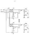
- Fig. 6 is a circuit diagram showing a conventional cold-cathode tube drive device for a long cold-cathode tube.
- Fig. 7 is a circuit diagram showing a conventional cold-cathode tube drive device for a plurality of the long cold-cathode tubes.
- the wiring 106b at the lower voltage side is directly connected to the ground in the vicinity of the cold-cathode tube 103, in which the lamp current value cannot be detected directly from the lower voltage side of the cold-cathode tube 103, so that the conducting current of the secondary winding of the booster transformer 102 is detected as a lamp current from the drop voltage by the resistor 111.
- Patent document 1 Japanese Patent Application Laid-Open No. 2004-213994 (Fig. 1).
- the conducting current value of the secondary winding of the transformer 102 is indirectly detected as a lamp current value, in which the current conducting a stray capacitance Cf between both the electrodes of the cold-cathode tube 103 and a stray capacitance between the cold-cathode tube 103 and a structure such as a panel are included in the current value to be detected, making it difficult to detect a precise lamp current value to control the current, light amount and so forth of the lamp precisely.
- the present invention has been made in consideration of the above-described problem, and an object thereof is to obtain a cold-cathode tube drive device capable of controlling current, a light amount and the like of a lamp precisely by detecting a lamp current value of a cold-cathode tube indirectly and precisely.
- a cold-cathode tube drive device includes: an inverter circuit generating a high-frequency voltage; a booster transformer boosting the high-frequency voltage generated by the inverter circuit; a cold-cathode tube which is turned on by the high-frequency voltage after boosted by the booster transformer; a series circuit having a reactance element and connected in parallel to the cold-cathode tube; a synthesis circuit combining the conducting current value of the series circuit with the secondary-side current value of the booster transformer so as to indirectly detect the lamp current value of the cold-cathode tube; and a control circuit controlling the inverter circuit according to the lamp current value indirectly detected by the synthesis circuit and controlling the lamp current of the cold-cathode tube.
- the impact of the conducting current of the stray capacitance on the current value detected indirectly is reduced by the synthesis circuit, so that the lamp current value of the cold-cathode tube can be detected indirectly and precisely, allowing the lamp current, the lamp light amount of and the like to be controlled precisely.
- the cold-cathode tube drive device may be as follows. Specifically, the synthesis circuit combines the conducting current value of the series circuit with the secondary-side current value of the booster transformer at a ratio of offsetting the conducting current value of the stray capacitance existing in parallel to the cold-cathode tube.
- the conducting current component of the stray capacitance is removed from the detected current value, allowing the lamp current value of the cold-cathode tube to be detected indirectly and more precisely, so that the lamp current, the lamp light amount and the like can be controlled more precisely.
- the cold-cathode tube drive device may be as follows. Specifically, as a reactance element of the series circuit, a resonant capacitor forming, together with the secondary wiring of the booster transformer, the resonant circuit is used.
- the resonant capacitor is used as a reactance element of the series circuit, when a series circuit connected in parallel to the cold-cathode tube and having the reactance element is provided, the number of the additionally-provided element can be reduced.
- the cold-cathode tube drive device detecting the lamp current value of the cold-cathode tube indirectly and precisely to control the lamp current, the lamp light amount and the like precisely can be obtained.
- Fig. 1 is a circuit diagram showing a configuration of a cold-cathode tube drive device according to a mode 1 of the present invention.
- an inverter circuit 1 is a circuit connected to a DC power source to generate a high-frequency voltage.
- a booster transformer 2 is a transformer boosting the high-frequency voltage generated by the inverter circuit 1.
- a cold-cathode tube 3 is a cold-cathode tube (CCFL), of which one end is connected to one end of a secondary wiring of the booster transformer 2 and the other end is connected to a ground in the vicinity thereof (a ground line, a structure serving as a ground, or the like).
- the cold-cathode tube 3 is a discharge tube being a tube in which electrons traveling between electrodes clash with an enclosed gas and the like to emit fluorescence.
- a resonant capacitor 4 is a reactance element forming, together with the secondary winding of the booster transformer 2, a resonant circuit.
- a resistance 5 is a resistance element connected in series to the resonant capacitor 4.
- One end of the resonant capacitor 4 is connected to one end of the cold-cathode tube 3 and the other end of the resonant capacitor 4 is connected to one end of the resistance 5.
- the other end of the resistance 5 is connected to a ground.
- This resonant capacitor 4 and the resistance 5 compose a series circuit 6 connected in parallel to the cold-cathode tube 3.
- a resistance 7 is a resistance element connected in series to the secondary wiring of the booster transformer 2. One end of the resistance 7 is connected to the other end of the secondary wiring of the booster transformer 2 and the other end of the resistance 7 is connected to a ground.
- a synthesis circuit 8 is a circuit combining a conducting current value i2 of the series circuit 6 and a secondary-side current value i l of the booster transformer 2 to indirectly detect a lamp current iL of the cold-cathode tube 3.
- one end of a resistance R1 is connected to one end of the resistance 7 and the other end of the secondary wiring of the booster transformer 2, and the other end of the resistance R1 is connected to one end of a resistance R2 and one end of a resistance R3.
- the other end of the resistance R2 is connected to the other end of the resonant capacitor 4 and one end of a resistance 5.
- the other end of the resistance 3 is connected to a ground.
- the one end of the resistance R1 and the other end of the resistance R2 perform as two input ends of the synthesis circuit 8, and the node of the other end of the resistance R1 and the one end of the resistance R2 performs an output end of the synthesis circuit 8.
- a control circuit 9 is a circuit controlling the inverter circuit 1 according to the lamp current value indirectly detected by the synthesis circuit 8 to control the lamp current, the lamp wattage, and so on of the cold-cathode tube 3. Since the lamp current varies backed by an individual difference between each cold-cathode tube 3, an ambient temperature, and the like, the control circuit 9 controls the inverter circuit 1 so that the lamp current does not vary by the above-described factors and becomes constant.
- the control circuit 9 is a circuit supplying a switching element of a not-shown full-bridge configuration in the inverter circuit 1 with a gate signal to perform PWM (Pulse Width Modulation) control. In the resent mode, the control circuit 9 is connected to the node of the resistances R1, R2, R3 in the synthesis circuit 8 via a diode D.
- stray capacitance Cf is generated between both the electrodes of the cold-cathode tube 3 caused by the cold-cathode tube 3 itself, a small clearance between the cold-cathode tube 3 and the structure such as the panel, and so forth.
- the value of this stray capacitance Cf depends mainly on the size of the clearance between the cold-cathode tube 3 and the structure such as a panel chassis to be the ground.
- the inverter circuit 1 generates a high-frequency voltage of a predetermined frequency and applies it to a primary winding of the booster transformer 2.
- the booster transformer 2 boosts the high-frequency voltage generated by the inverter circuit 1.
- the voltage induced in the secondary winding of the booster transformer 2 is applied to the cold-cathode tube 3 and the like. With this, the lamp current iL is conducted to cause the cold-cathode tube 3 to emit light.
- the control circuit 9 controls the inverter circuit 1 according to the value of the lamp current iL indirectly detected by the synthesis circuit 8 to control the lamp current iL, the lamp wattage, and so on.
- a combined current in which the lamp current, the conducting current of the stray capacitance Cf, and the like are combined, flows in the resistance 7 and the secondary side of the booster transformer 2, and the current value becomes i1.
- Fig. 2 is a view illustrating a relation between the secondary-side current value i1 of the booster transformer 2 and the conducting current value i2 of the series circuit 6 in the cold-cathode tube drive device according to the mode of the present invention. As shown in Fig. 2, the phase of the current value i2 deviates from the phase of the current value i1.
- R7 is defined as the resistance value of the resistance 7
- a combined current value i3 becomes approximately (- i1 ⁇ R7 / (R1 + R3) + i2 ⁇ R5 /(R2 + R3)).
- the weighted difference between the conducting current value i1 of the resistance 7 and the conducting current value i2 of the resistance 5 is the combined current value i3.
- the combined ratio of the conducting current value i1 of the resistance 7 and the conducting current value i2 of the resistance 5 is adjustable at the ratio of the resistance values R5, R7 of the resistances 5, 7. Accordingly, the values of the resistances R5, R7 may be adjusted at the time of a trial manufacturing or a manufacturing of a liquid panel so that the lamp current iL and the combined current i3 coincide to be agreed or resemble, as an example. Further, for the purpose of easing the adjustment, it is acceptable that the resistances R5, R7 are variable resistances. Or otherwise, in place of the values of the resistances R5, R7 or in addition to the values of the resistances R5, R7, the values of the resistances R1, R2, R3 may be adjusted.
- the current value i1 of the resistance 7 contains the component of conducting current iC of the stray capacitance Cf, as described above, hence, the phase of the current value i1 of the resistance 7 deviates from the phase of the lamp current iL to the extent thereof.
- the synthesis circuit 8 by obtaining the difference between the current value i1 and the current value i2 of which phase deviates from the phase of the current value i1 in the manner as described above, a part or all of the component of the conducting current iC of the stray capacitance Cf in the current value i1 of the resistance 7 is/are offset, so that the current value close to the lamp current value iL can be obtained from the current value i1 of the resistance 7, as a combined current value i3.
- the combined current value i3 can be obtained in the synthesis circuit 8, and this current value is detected as a voltage of both the electrodes of the resistance R3.
- the control circuit 9 detects the voltage of both the electrodes of the resistance R3 via the diode D, and the combined current value i3 based thereon is defined as the lamp current value iL indirectly detected, to control the inverter circuit 1 based on the lamp current value iL.
- Fig. 3 is view to illustrate an effect of the cold-cathode tube drive device according to the mode of the present invention.
- a comparison is made between a actually measured waveform of the lamp current value iL being measured directly by inserting a resistance on the lower voltage side of the cold-cathode tube 3 of the circuit shown in Fig. 1 and a actually measured waveform of the combined current i3 in the synthesis circuit 8. As shown in Fig.
- the series circuit 6 having the capacitor 4 is connected in parallel to the cold-cathode tube 3, and the synthesis circuit 8 combines the conducting current value i2 of the series circuit 6 and the secondary-side current value i1 of the booster transformer 2 to detect the lamp current value iL of the cold-cathode tube 3 indirectly.
- the control circuit 9 controls the inverter circuit 1 based on the value of the lamp current value iL indirectly detected by the synthesis circuit 8 to control the lamp current of the cold-cathode tube 3.
- the impact of the conducting current iC of the stray capacitance Cf on the current value iL indirectly detected is reduced by the synthesis circuit 8, hence, by detecting the lamp current value iL of the cold-cathode tube 3 indirectly and precisely, the lamp current, the lamp light amount, and the like can be controlled precisely. Further, when the plurality of cold-cathode tubes 3 are used as a backlight, the light amounts of the respective cold-cathode tubes 3 can be controlled precisely, so that luminance unevenness of the liquid display panel can be prevented from arising.
- the synthesis circuit 8 combines the secondary-side current value i1 of the booster transformer 2 with the conducting current value i2 of the series circuit 6 at the ratio of offsetting the conducting current value iC of the stray capacitance Cf existing in parallel to the cold-cathode tube 3.
- the current value i3 in which the conducting current component iC of the stray capacitance Cf is removed is obtained, allowing the lamp current value iL of the cold-cathode tube 3 to be detected indirectly and more precisely, so that the lamp current, the lamp light amount and the like can be controlled more precisely.
- the resonant capacitor 4 forming, together with the secondary wiring of the booster transformer 2, the resonant circuit is used.
- the resonant capacitor 4 is used as a reactance element of the series circuit 6, when the series circuit 6 connected in parallel to the cold-cathode tube 3 and having the reactance element is provided, the number of the additionally-provided element can be reduced.
- a cold-cathode tube drive device is a device driving a plurality of cold-cathode tubes.
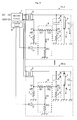
- Fig. 5 is a circuit diagram showing a configuration of the cold-cathode tube drive device according to the mode 2 of the present invention.
- the respective driving sections 21-i include the same booster transformer 2, cold-cathode tube 3, series circuit 6, resistance 7, synthesis circuit 8 and diode D as in Fig. 1, respectively.
- the control circuit 9 controls the inverter circuit 1 based on the lamp current values indirectly detected by the synthesis circuits 8 in the driving sections 21-1 to 21-n to thereby control the lamp currents, the lamp wattages, and the like of the cold-cathode tubes 3 in the driving sections 21-1 to 21-n.
- the same effect as in the mode 1 can be obtained.
- the plurality of the cold-cathode tubes 3 are used as a backlight, the light amounts of the respective cold-cathode tubes 3 can be controlled precisely, so that the luminance unevenness of the liquid display panel can be prevented from arising.
- the resonant capacitor 4 is used as a reactance element of the series circuit 6, however, instead, the series circuit 6 may be provided independently of the resonant capacitor 4.
- the current value i1 (voltage value v1) and the current value i2 (voltage value v2) are combined by the synthesis circuit 8 composed of the three resistances R1, R2, R3, however, instead, the current value i1 (voltage value v1) and the current value i2 (voltage value v2) may be combined using an active element such as a transistor or an operational amplifier.
- the present invention is applicable to, for example, the cold-cathode tube drive device to drive each of the plurality of long cold-cathode tubes composing the backlight of the liquid crystal display panel of a size of 20 inches or more.
Landscapes
- Circuit Arrangements For Discharge Lamps (AREA)
Abstract
Description
- The present invention relates to a cold-cathode tube drive device.
- Conventionally, a plurality of cold-cathode tubes (CCFLs: Cold Cathode Fluorescent Lamps) are used for a backlight of a liquid crystal display panel in a liquid crystal television receiver (hereinafter referred to as the "liquid crystal TV"), a liquid crystal monitor, or the like (see, for example,
Japanese Patent Application Laid-Open No. 2004-213994 - Fig. 4 is a circuit diagram showing a conventional cold-cathode tube drive device. In the device shown in Fig. 4, an
inverter circuit 101 generates a high-frequency voltage, abooster transformer 102 boosts the high-frequency voltage generated by theinverter circuit 101 to apply the high-frequency voltage after boosted to a cold-cathode tube 103. Aresonant capacitor 104 is a capacitor composing, together with a secondary winding of thebooster transformer 102, a resonant circuit. - The
inverter circuit 101 acquires a drop voltage by aresistor 105 via a diode D and detects a conducting current value of the cold-cathode tube 103 based thereon to thereby control lamp current of the cold-cathode tube 103 in accordance with the value. - Based on the circuit configuration as described above, the lamp current of the cold-
cathode tube 103 is detected directly from a lower voltage portion of the cold-cathode tube 103. - In a liquid crystal display panel of a medium-size or below, the cold-
cathode tube 103 is relatively short, in which stray capacitance caused by twowirings cathode tube 103 has a smaller impact, so that one of the twowirings cathode tube 103 is integrated into the other. - Meanwhile, in a liquid crystal display panel of a large size, namely a widescreen being developed recently, the cold-
cathode tube 103 of a long size is used and thereby the twowirings wirings inverter circuit 101 are caused. - Therefore, when the long cold-
cathode tube 103 is used, the one of the twowirings cathode tube 103 is not integrated into the other, and, instead, thewiring 106b at the lower voltage side is directly connected to a case or the like in the vicinity of the root of the cold-cathode tube 103 as a ground. Fig. 6 is a circuit diagram showing a conventional cold-cathode tube drive device for a long cold-cathode tube. In addition, Fig. 7 is a circuit diagram showing a conventional cold-cathode tube drive device for a plurality of the long cold-cathode tubes. - In the above cases, the
wiring 106b at the lower voltage side is directly connected to the ground in the vicinity of the cold-cathode tube 103, in which the lamp current value cannot be detected directly from the lower voltage side of the cold-cathode tube 103, so that the conducting current of the secondary winding of thebooster transformer 102 is detected as a lamp current from the drop voltage by theresistor 111. - Patent document 1:
Japanese Patent Application Laid-Open No. 2004-213994 - However, in the conventional cold-cathode tube drive device for the long cold-cathode tube, the conducting current value of the secondary winding of the
transformer 102 is indirectly detected as a lamp current value, in which the current conducting a stray capacitance Cf between both the electrodes of the cold-cathode tube 103 and a stray capacitance between the cold-cathode tube 103 and a structure such as a panel are included in the current value to be detected, making it difficult to detect a precise lamp current value to control the current, light amount and so forth of the lamp precisely. - The present invention has been made in consideration of the above-described problem, and an object thereof is to obtain a cold-cathode tube drive device capable of controlling current, a light amount and the like of a lamp precisely by detecting a lamp current value of a cold-cathode tube indirectly and precisely.
- In order to bring a solution to the above-described problem, the present invention is as described below.
- A cold-cathode tube drive device according to the present invention includes: an inverter circuit generating a high-frequency voltage; a booster transformer boosting the high-frequency voltage generated by the inverter circuit; a cold-cathode tube which is turned on by the high-frequency voltage after boosted by the booster transformer; a series circuit having a reactance element and connected in parallel to the cold-cathode tube; a synthesis circuit combining the conducting current value of the series circuit with the secondary-side current value of the booster transformer so as to indirectly detect the lamp current value of the cold-cathode tube; and a control circuit controlling the inverter circuit according to the lamp current value indirectly detected by the synthesis circuit and controlling the lamp current of the cold-cathode tube.
- With this, the impact of the conducting current of the stray capacitance on the current value detected indirectly is reduced by the synthesis circuit, so that the lamp current value of the cold-cathode tube can be detected indirectly and precisely, allowing the lamp current, the lamp light amount of and the like to be controlled precisely.
- Further, in addition to the above-described cold-cathode tube drive device, the cold-cathode tube drive device according to the present invention may be as follows. Specifically, the synthesis circuit combines the conducting current value of the series circuit with the secondary-side current value of the booster transformer at a ratio of offsetting the conducting current value of the stray capacitance existing in parallel to the cold-cathode tube.
- With this, the conducting current component of the stray capacitance is removed from the detected current value, allowing the lamp current value of the cold-cathode tube to be detected indirectly and more precisely, so that the lamp current, the lamp light amount and the like can be controlled more precisely.
- Further, in addition to any one of the above-described cold-cathode tube drive devices, the cold-cathode tube drive device according to the present invention may be as follows. Specifically, as a reactance element of the series circuit, a resonant capacitor forming, together with the secondary wiring of the booster transformer, the resonant circuit is used.
- With this, since the resonant capacitor is used as a reactance element of the series circuit, when a series circuit connected in parallel to the cold-cathode tube and having the reactance element is provided, the number of the additionally-provided element can be reduced.
- According to the present invention, the cold-cathode tube drive device detecting the lamp current value of the cold-cathode tube indirectly and precisely to control the lamp current, the lamp light amount and the like precisely can be obtained.
-
- [Fig. 1]Fig. 1 is a circuit diagram showing a configuration of a cold-cathode tube drive device according to a mode of the present invention;
- [Fig. 2]Fig. 2 is a view illustrating a relation between a secondary-side current value of a booster transformer and a conducting current value of a series circuit in the cold-cathode tube drive device according to the mode of the present invention;
- [Fig. 3]Fig. 3 is view to illustrate an effect of the cold-cathode tube drive device according to the mode of the present invention;
- [Fig.4]Fig. 4 is a circuit diagram showing a conventional cold-cathode tube drive device;
- [Fig. 5]Fig. 5 is a circuit diagram showing a configuration of a cold-cathode tube drive device according to a
mode 2 of the present invention; - [Fig.6]Fig. 6 is a circuit diagram showing a conventional cold-cathode tube drive device for a long cold-cathode tube; and
- [Fig. 7] Fig. 7 is a circuit diagram showing a conventional cold-cathode tube drive device for a plurality of the long cold-cathode tubes.
-
- 1. inverter circuit
- 2. booster transformer
- 3. cold-cathode tube
- 4. resonant capacitor (reactance element)
- 6. series circuit
- 8. synthesis circuit
- 9. control circuit
- Hereinafter, modes according to the present invention will be described based on the drawings.
- Fig. 1 is a circuit diagram showing a configuration of a cold-cathode tube drive device according to a
mode 1 of the present invention. In Fig. 1, aninverter circuit 1 is a circuit connected to a DC power source to generate a high-frequency voltage. Abooster transformer 2 is a transformer boosting the high-frequency voltage generated by theinverter circuit 1. - A cold-
cathode tube 3 is a cold-cathode tube (CCFL), of which one end is connected to one end of a secondary wiring of thebooster transformer 2 and the other end is connected to a ground in the vicinity thereof (a ground line, a structure serving as a ground, or the like). The cold-cathode tube 3 is a discharge tube being a tube in which electrons traveling between electrodes clash with an enclosed gas and the like to emit fluorescence. - Further, a resonant capacitor 4 is a reactance element forming, together with the secondary winding of the
booster transformer 2, a resonant circuit. Aresistance 5 is a resistance element connected in series to the resonant capacitor 4. One end of the resonant capacitor 4 is connected to one end of the cold-cathode tube 3 and the other end of the resonant capacitor 4 is connected to one end of theresistance 5. The other end of theresistance 5 is connected to a ground. This resonant capacitor 4 and theresistance 5 compose aseries circuit 6 connected in parallel to the cold-cathode tube 3. - Further, a resistance 7 is a resistance element connected in series to the secondary wiring of the
booster transformer 2. One end of the resistance 7 is connected to the other end of the secondary wiring of thebooster transformer 2 and the other end of the resistance 7 is connected to a ground. - Further, a
synthesis circuit 8 is a circuit combining a conducting current value i2 of theseries circuit 6 and a secondary-side current value i l of thebooster transformer 2 to indirectly detect a lamp current iL of the cold-cathode tube 3. - In the
synthesis circuit 8, one end of a resistance R1 is connected to one end of the resistance 7 and the other end of the secondary wiring of thebooster transformer 2, and the other end of the resistance R1 is connected to one end of a resistance R2 and one end of a resistance R3. The other end of the resistance R2 is connected to the other end of the resonant capacitor 4 and one end of aresistance 5. The other end of theresistance 3 is connected to a ground. In other words, the one end of the resistance R1 and the other end of the resistance R2 perform as two input ends of thesynthesis circuit 8, and the node of the other end of the resistance R1 and the one end of the resistance R2 performs an output end of thesynthesis circuit 8. - Further, a
control circuit 9 is a circuit controlling theinverter circuit 1 according to the lamp current value indirectly detected by thesynthesis circuit 8 to control the lamp current, the lamp wattage, and so on of the cold-cathode tube 3. Since the lamp current varies backed by an individual difference between each cold-cathode tube 3, an ambient temperature, and the like, thecontrol circuit 9 controls theinverter circuit 1 so that the lamp current does not vary by the above-described factors and becomes constant. For instance, thecontrol circuit 9 is a circuit supplying a switching element of a not-shown full-bridge configuration in theinverter circuit 1 with a gate signal to perform PWM (Pulse Width Modulation) control. In the resent mode, thecontrol circuit 9 is connected to the node of the resistances R1, R2, R3 in thesynthesis circuit 8 via a diode D. - Further, stray capacitance Cf is generated between both the electrodes of the cold-
cathode tube 3 caused by the cold-cathode tube 3 itself, a small clearance between the cold-cathode tube 3 and the structure such as the panel, and so forth. The value of this stray capacitance Cf depends mainly on the size of the clearance between the cold-cathode tube 3 and the structure such as a panel chassis to be the ground. - Subsequently, the description will be given of the operation of the above-described device.
- The
inverter circuit 1 generates a high-frequency voltage of a predetermined frequency and applies it to a primary winding of thebooster transformer 2. Thebooster transformer 2 boosts the high-frequency voltage generated by theinverter circuit 1. The voltage induced in the secondary winding of thebooster transformer 2 is applied to the cold-cathode tube 3 and the like. With this, the lamp current iL is conducted to cause the cold-cathode tube 3 to emit light. - The
control circuit 9 controls theinverter circuit 1 according to the value of the lamp current iL indirectly detected by thesynthesis circuit 8 to control the lamp current iL, the lamp wattage, and so on. - Here, the detection of the lamp current value iL by the
synthesis circuit 8 will be described. - Immediately after the light emission, a combined current, in which the lamp current, the conducting current of the stray capacitance Cf, and the like are combined, flows in the resistance 7 and the secondary side of the
booster transformer 2, and the current value becomes i1. - In addition, the resonant capacitor 4 exists in the
series circuit 6, in which the phase of the conducting current of theseries circuit 6 deviates from the phase of the conducting current of the resistance 7, namely the phase of the secondary side current of thebooster transformer 2. The amount of the phase deviation is approximately (90 + 45) degrees. Fig. 2 is a view illustrating a relation between the secondary-side current value i1 of thebooster transformer 2 and the conducting current value i2 of theseries circuit 6 in the cold-cathode tube drive device according to the mode of the present invention. As shown in Fig. 2, the phase of the current value i2 deviates from the phase of the current value i1. - In the
synthesis circuit 8, in accordance with a voltage v1 (= - R7 × i1, R7 is defined as the resistance value of the resistance 7) at both the ends of the resistance 7 and a voltage v2 (= R5 × i2, R5 is defined as the resistance value of the resistance 5) at both the ends of theresistance 5, a combined current value i3 becomes approximately (- i1 × R7 / (R1 + R3) + i2 × R5 /(R2 + R3)). Specifically, the weighted difference between the conducting current value i1 of the resistance 7 and the conducting current value i2 of theresistance 5 is the combined current value i3. - Further, the combined ratio of the conducting current value i1 of the resistance 7 and the conducting current value i2 of the
resistance 5 is adjustable at the ratio of the resistance values R5, R7 of theresistances 5, 7. Accordingly, the values of the resistances R5, R7 may be adjusted at the time of a trial manufacturing or a manufacturing of a liquid panel so that the lamp current iL and the combined current i3 coincide to be agreed or resemble, as an example. Further, for the purpose of easing the adjustment, it is acceptable that the resistances R5, R7 are variable resistances. Or otherwise, in place of the values of the resistances R5, R7 or in addition to the values of the resistances R5, R7, the values of the resistances R1, R2, R3 may be adjusted. - Meanwhile, the current value i1 of the resistance 7 contains the component of conducting current iC of the stray capacitance Cf, as described above, hence, the phase of the current value i1 of the resistance 7 deviates from the phase of the lamp current iL to the extent thereof. Therefore, in the
synthesis circuit 8, by obtaining the difference between the current value i1 and the current value i2 of which phase deviates from the phase of the current value i1 in the manner as described above, a part or all of the component of the conducting current iC of the stray capacitance Cf in the current value i1 of the resistance 7 is/are offset, so that the current value close to the lamp current value iL can be obtained from the current value i1 of the resistance 7, as a combined current value i3. - Thus, the combined current value i3 can be obtained in the
synthesis circuit 8, and this current value is detected as a voltage of both the electrodes of the resistance R3. - The
control circuit 9 detects the voltage of both the electrodes of the resistance R3 via the diode D, and the combined current value i3 based thereon is defined as the lamp current value iL indirectly detected, to control theinverter circuit 1 based on the lamp current value iL. - Fig. 3 is view to illustrate an effect of the cold-cathode tube drive device according to the mode of the present invention. In Fig. 3, in order to verify the effect of the cold-cathode tube drive device, a comparison is made between a actually measured waveform of the lamp current value iL being measured directly by inserting a resistance on the lower voltage side of the cold-
cathode tube 3 of the circuit shown in Fig. 1 and a actually measured waveform of the combined current i3 in thesynthesis circuit 8. As shown in Fig. 3, by combining the secondary-side current value i1 of thebooster transformer 2 and the current value i2 of theseries circuit 6 at the predetermined ratio, the combined current i3 almost coinciding as well as resembling the directly measured lamp current value iL can be obtained. - As has been described above, according to the
mode 1 above, theseries circuit 6 having the capacitor 4 is connected in parallel to the cold-cathode tube 3, and thesynthesis circuit 8 combines the conducting current value i2 of theseries circuit 6 and the secondary-side current value i1 of thebooster transformer 2 to detect the lamp current value iL of the cold-cathode tube 3 indirectly. Based on the above, thecontrol circuit 9 controls theinverter circuit 1 based on the value of the lamp current value iL indirectly detected by thesynthesis circuit 8 to control the lamp current of the cold-cathode tube 3. - With this, the impact of the conducting current iC of the stray capacitance Cf on the current value iL indirectly detected is reduced by the
synthesis circuit 8, hence, by detecting the lamp current value iL of the cold-cathode tube 3 indirectly and precisely, the lamp current, the lamp light amount, and the like can be controlled precisely. Further, when the plurality of cold-cathode tubes 3 are used as a backlight, the light amounts of the respective cold-cathode tubes 3 can be controlled precisely, so that luminance unevenness of the liquid display panel can be prevented from arising. - Furthermore, according to the
mode 1 described above, thesynthesis circuit 8 combines the secondary-side current value i1 of thebooster transformer 2 with the conducting current value i2 of theseries circuit 6 at the ratio of offsetting the conducting current value iC of the stray capacitance Cf existing in parallel to the cold-cathode tube 3. - Through this, the current value i3 in which the conducting current component iC of the stray capacitance Cf is removed is obtained, allowing the lamp current value iL of the cold-
cathode tube 3 to be detected indirectly and more precisely, so that the lamp current, the lamp light amount and the like can be controlled more precisely. - Further, according to the
mode 1 described above, as a reactance element of theseries circuit 6, the resonant capacitor 4 forming, together with the secondary wiring of thebooster transformer 2, the resonant circuit is used. - With this, since the resonant capacitor 4 is used as a reactance element of the
series circuit 6, when theseries circuit 6 connected in parallel to the cold-cathode tube 3 and having the reactance element is provided, the number of the additionally-provided element can be reduced. - A cold-cathode tube drive device according to a
mode 2 of the present invention is a device driving a plurality of cold-cathode tubes. Fig. 5 is a circuit diagram showing a configuration of the cold-cathode tube drive device according to themode 2 of the present invention. In Fig. 5, each of driving sections 21-i (i = 1, ..., n, n > 1) are a circuit driving a single cold-cathode tube 3 based on the high-frequency voltage outputted by theinverter circuit 1. The respective driving sections 21-i include thesame booster transformer 2, cold-cathode tube 3,series circuit 6, resistance 7,synthesis circuit 8 and diode D as in Fig. 1, respectively. In themode 2, thecontrol circuit 9 controls theinverter circuit 1 based on the lamp current values indirectly detected by thesynthesis circuits 8 in the driving sections 21-1 to 21-n to thereby control the lamp currents, the lamp wattages, and the like of the cold-cathode tubes 3 in the driving sections 21-1 to 21-n. - Note that, as for the other configuration in Fig. 5, those denoted by the same numerical references as in the mode 1 (Fig. 1) have the same configurations as of the
mode 1, respectively, so that the description thereof will be omitted here. Also, the operations of the respective driving sections 21-i are the same as of the same circuit portion of themode 1, so that the description thereof will be omitted here. - As has been described above, according to the above-described
mode 2, even when the plurality of cold-cathode tubes 3 are turned on, the same effect as in themode 1 can be obtained. In other words, when the plurality of the cold-cathode tubes 3 are used as a backlight, the light amounts of the respective cold-cathode tubes 3 can be controlled precisely, so that the luminance unevenness of the liquid display panel can be prevented from arising. - Note that the above-described respective modes are preferred examples of the present invention, however, the present invention is not limited to the above and can be modified or altered in various manner without departing from the scope of the present invention.
- For instance, in the above-described first and
mode 2, the resonant capacitor 4 is used as a reactance element of theseries circuit 6, however, instead, theseries circuit 6 may be provided independently of the resonant capacitor 4. - Further, in the above-described first and
mode 2, the current value i1 (voltage value v1) and the current value i2 (voltage value v2) are combined by thesynthesis circuit 8 composed of the three resistances R1, R2, R3, however, instead, the current value i1 (voltage value v1) and the current value i2 (voltage value v2) may be combined using an active element such as a transistor or an operational amplifier. - The present invention is applicable to, for example, the cold-cathode tube drive device to drive each of the plurality of long cold-cathode tubes composing the backlight of the liquid crystal display panel of a size of 20 inches or more.
Claims (3)
- A cold-cathode tube drive device comprising:an inverter circuit generating a high-frequency voltage;a booster transformer boosting the high-frequency voltage generated by said inverter circuit;a cold-cathode tube which is turned on by the high-frequency voltage after boosted by said booster transformer;a series circuit having a reactance element and connected in parallel to said cold-cathode tube;a synthesis circuit combining the conducting current value of the series circuit with the secondary-side current value of said booster transformer so as to indirectly detect the lamp current value of said cold-cathode tube; anda control circuit controlling said inverter circuit according to the lamp current value indirectly detected by said synthesis circuit and controlling the lamp current of said cold-cathode tube.
- The cold-cathode tube drive device according to claim 1,
wherein said synthesis circuit combines the conducting current value of said series circuit with the secondary-side current value of said booster transformer at a ratio of offsetting the conducting current value of the stray capacitance existing in parallel to said cold-cathode tube. - The cold-cathode tube drive device according to claim 1 or claim 2,
wherein the reactance element of said series circuit is a resonant condenser forming, together with the secondary wiring of said booster transformer, the resonant circuit.
Applications Claiming Priority (2)
| Application Number | Priority Date | Filing Date | Title |
|---|---|---|---|
| JP2004303123A JP4446476B2 (en) | 2004-10-18 | 2004-10-18 | Cold cathode tube drive |
| PCT/JP2005/014497 WO2006043361A1 (en) | 2004-10-18 | 2005-08-08 | Cold-cathode tube drive device |
Publications (3)
| Publication Number | Publication Date |
|---|---|
| EP1863325A1 true EP1863325A1 (en) | 2007-12-05 |
| EP1863325A4 EP1863325A4 (en) | 2009-12-30 |
| EP1863325B1 EP1863325B1 (en) | 2011-06-22 |
Family
ID=36202785
Family Applications (1)
| Application Number | Title | Priority Date | Filing Date |
|---|---|---|---|
| EP05768535A Expired - Lifetime EP1863325B1 (en) | 2004-10-18 | 2005-08-08 | Cold-cathode tube drive device |
Country Status (8)
| Country | Link |
|---|---|
| US (1) | US7656101B2 (en) |
| EP (1) | EP1863325B1 (en) |
| JP (1) | JP4446476B2 (en) |
| KR (1) | KR100824710B1 (en) |
| CN (1) | CN101019469B (en) |
| AT (1) | ATE514317T1 (en) |
| TW (1) | TW200614875A (en) |
| WO (1) | WO2006043361A1 (en) |
Families Citing this family (4)
| Publication number | Priority date | Publication date | Assignee | Title |
|---|---|---|---|---|
| JP2009009721A (en) * | 2007-06-26 | 2009-01-15 | Sanken Electric Co Ltd | Discharge lamp lighting device |
| JP2009032421A (en) * | 2007-07-24 | 2009-02-12 | Sanken Electric Co Ltd | Discharge lamp lighting device |
| TW201034518A (en) * | 2009-03-05 | 2010-09-16 | Delta Electronics Inc | Lamp driving system |
| CN101835325A (en) * | 2009-03-10 | 2010-09-15 | 台达电子工业股份有限公司 | Lamp tube driving system |
Family Cites Families (12)
| Publication number | Priority date | Publication date | Assignee | Title |
|---|---|---|---|---|
| JPS61154486A (en) * | 1984-12-27 | 1986-07-14 | Stanley Electric Co Ltd | Inverter |
| JP3096242B2 (en) * | 1995-08-30 | 2000-10-10 | 日本政策投資銀行 | Optical disk curing device |
| JPH09129382A (en) * | 1995-10-17 | 1997-05-16 | Internatl Business Mach Corp <Ibm> | Detector and information processing system for anomaly in discharge tube circuit |
| EP0782374B1 (en) * | 1995-12-26 | 1999-10-27 | Tokin Corporation | Inverter circuit for lighting a cold-cathode tube by the use of a piezoelectric transformer |
| DE19613257A1 (en) | 1996-01-26 | 1997-07-31 | Tridonic Bauelemente | Method and electronic control circuit for regulating the operating behavior of gas discharge lamps |
| EP0910229A3 (en) * | 1997-10-16 | 1999-08-25 | Tokin Corporation | Cold-cathode tube lighting circuit with protection circuit for piezoelectric transformer |
| US5969482A (en) * | 1998-11-30 | 1999-10-19 | Philips Electronics North America Corporation | Circuit arrangement for operating a discharge lamp including real power sensing using a single quadrant multiplier |
| US6100647A (en) * | 1998-12-28 | 2000-08-08 | Philips Electronics North America Corp. | Lamp ballast for accurate control of lamp intensity |
| US6420839B1 (en) | 2001-01-19 | 2002-07-16 | Ambit Microsystems Corp. | Power supply system for multiple loads and driving system for multiple lamps |
| JP2004213994A (en) * | 2002-12-27 | 2004-07-29 | Harison Toshiba Lighting Corp | Discharge lamp lighting device |
| JP3096242U (en) * | 2003-03-04 | 2003-09-12 | 船井電機株式会社 | Television receivers and cold cathode tube dimmers |
| JP4716105B2 (en) * | 2005-11-14 | 2011-07-06 | ミネベア株式会社 | Discharge lamp lighting device |
-
2004
- 2004-10-18 JP JP2004303123A patent/JP4446476B2/en not_active Expired - Fee Related
-
2005
- 2005-08-08 WO PCT/JP2005/014497 patent/WO2006043361A1/en not_active Ceased
- 2005-08-08 US US11/577,437 patent/US7656101B2/en not_active Expired - Fee Related
- 2005-08-08 KR KR1020077006941A patent/KR100824710B1/en not_active Expired - Fee Related
- 2005-08-08 CN CN200580030562XA patent/CN101019469B/en not_active Expired - Fee Related
- 2005-08-08 EP EP05768535A patent/EP1863325B1/en not_active Expired - Lifetime
- 2005-08-08 AT AT05768535T patent/ATE514317T1/en not_active IP Right Cessation
- 2005-10-07 TW TW094135115A patent/TW200614875A/en not_active IP Right Cessation
Also Published As
| Publication number | Publication date |
|---|---|
| EP1863325B1 (en) | 2011-06-22 |
| KR20070057206A (en) | 2007-06-04 |
| TWI347801B (en) | 2011-08-21 |
| KR100824710B1 (en) | 2008-04-24 |
| JP4446476B2 (en) | 2010-04-07 |
| WO2006043361A1 (en) | 2006-04-27 |
| CN101019469A (en) | 2007-08-15 |
| EP1863325A4 (en) | 2009-12-30 |
| ATE514317T1 (en) | 2011-07-15 |
| CN101019469B (en) | 2010-07-07 |
| JP2006114441A (en) | 2006-04-27 |
| US20090045756A1 (en) | 2009-02-19 |
| US7656101B2 (en) | 2010-02-02 |
| TW200614875A (en) | 2006-05-01 |
Similar Documents
| Publication | Publication Date | Title |
|---|---|---|
| US7489087B2 (en) | Backlight inverter and method of driving same | |
| US20090179581A1 (en) | Inverter circuit, backlight assembly and liquid crystal display having the same, and method thereof | |
| JP2002203689A (en) | Driving device for cold cathode fluorescent tube using piezoelectric transformer and driving method thereof | |
| JP2005063970A (en) | Lamp driving method and apparatus, and backlight assembly and liquid crystal display device including the apparatus | |
| KR20060053986A (en) | Discharge lamp lighting device | |
| CN101317324B (en) | Power supply device, light emitting device and electronic equipment using the same | |
| JP2006024511A (en) | Discharge lamp lighting device | |
| US7315133B2 (en) | Discharge lamp lighting apparatus | |
| EP1863325B1 (en) | Cold-cathode tube drive device | |
| US7235931B2 (en) | Discharge lamp lighting apparatus for lighting multiple discharge lamps | |
| US7230390B2 (en) | Cold cathode fluorescent lamp assembly | |
| JP4125687B2 (en) | Discharge tube lighting control circuit and abnormality detection circuit thereof | |
| JP2005190835A (en) | Backlight device for liquid crystal television | |
| US7791283B2 (en) | Discharge lamp lighting apparatus | |
| JP3513515B2 (en) | CCFL driver circuit | |
| JP3975727B2 (en) | Flat plate light source device | |
| KR20040058071A (en) | Dielectric barrier discharge lamp lighting apparatus | |
| JP2007265897A (en) | Inverter circuit for discharge tube | |
| JP2004328951A (en) | Inverter transformer | |
| JP2004327352A (en) | CCFL lighting circuit | |
| KR20040089778A (en) | Circuit for Controlling Driving Frequency of Lamp for Back Light | |
| JP2005143253A (en) | Inverter drive circuit |
Legal Events
| Date | Code | Title | Description |
|---|---|---|---|
| PUAI | Public reference made under article 153(3) epc to a published international application that has entered the european phase |
Free format text: ORIGINAL CODE: 0009012 |
|
| 17P | Request for examination filed |
Effective date: 20070404 |
|
| AK | Designated contracting states |
Kind code of ref document: A1 Designated state(s): AT BE BG CH CY CZ DE DK EE ES FI FR GB GR HU IE IS IT LI LT LU LV MC NL PL PT RO SE SI SK TR |
|
| DAX | Request for extension of the european patent (deleted) | ||
| A4 | Supplementary search report drawn up and despatched |
Effective date: 20091201 |
|
| 17Q | First examination report despatched |
Effective date: 20100308 |
|
| RIC1 | Information provided on ipc code assigned before grant |
Ipc: H05B 41/392 20060101ALI20101111BHEP Ipc: H05B 41/24 20060101AFI20101111BHEP |
|
| GRAP | Despatch of communication of intention to grant a patent |
Free format text: ORIGINAL CODE: EPIDOSNIGR1 |
|
| GRAS | Grant fee paid |
Free format text: ORIGINAL CODE: EPIDOSNIGR3 |
|
| GRAA | (expected) grant |
Free format text: ORIGINAL CODE: 0009210 |
|
| AK | Designated contracting states |
Kind code of ref document: B1 Designated state(s): AT BE BG CH CY CZ DE DK EE ES FI FR GB GR HU IE IS IT LI LT LU LV MC NL PL PT RO SE SI SK TR |
|
| REG | Reference to a national code |
Ref country code: GB Ref legal event code: FG4D |
|
| REG | Reference to a national code |
Ref country code: CH Ref legal event code: EP |
|
| REG | Reference to a national code |
Ref country code: IE Ref legal event code: FG4D |
|
| REG | Reference to a national code |
Ref country code: DE Ref legal event code: R096 Ref document number: 602005028659 Country of ref document: DE Effective date: 20110811 |
|
| REG | Reference to a national code |
Ref country code: NL Ref legal event code: VDEP Effective date: 20110622 |
|
| PG25 | Lapsed in a contracting state [announced via postgrant information from national office to epo] |
Ref country code: LT Free format text: LAPSE BECAUSE OF FAILURE TO SUBMIT A TRANSLATION OF THE DESCRIPTION OR TO PAY THE FEE WITHIN THE PRESCRIBED TIME-LIMIT Effective date: 20110622 Ref country code: SE Free format text: LAPSE BECAUSE OF FAILURE TO SUBMIT A TRANSLATION OF THE DESCRIPTION OR TO PAY THE FEE WITHIN THE PRESCRIBED TIME-LIMIT Effective date: 20110622 |
|
| PG25 | Lapsed in a contracting state [announced via postgrant information from national office to epo] |
Ref country code: FI Free format text: LAPSE BECAUSE OF FAILURE TO SUBMIT A TRANSLATION OF THE DESCRIPTION OR TO PAY THE FEE WITHIN THE PRESCRIBED TIME-LIMIT Effective date: 20110622 Ref country code: LV Free format text: LAPSE BECAUSE OF FAILURE TO SUBMIT A TRANSLATION OF THE DESCRIPTION OR TO PAY THE FEE WITHIN THE PRESCRIBED TIME-LIMIT Effective date: 20110622 Ref country code: GR Free format text: LAPSE BECAUSE OF FAILURE TO SUBMIT A TRANSLATION OF THE DESCRIPTION OR TO PAY THE FEE WITHIN THE PRESCRIBED TIME-LIMIT Effective date: 20110923 Ref country code: SI Free format text: LAPSE BECAUSE OF FAILURE TO SUBMIT A TRANSLATION OF THE DESCRIPTION OR TO PAY THE FEE WITHIN THE PRESCRIBED TIME-LIMIT Effective date: 20110622 Ref country code: AT Free format text: LAPSE BECAUSE OF FAILURE TO SUBMIT A TRANSLATION OF THE DESCRIPTION OR TO PAY THE FEE WITHIN THE PRESCRIBED TIME-LIMIT Effective date: 20110622 Ref country code: CY Free format text: LAPSE BECAUSE OF FAILURE TO SUBMIT A TRANSLATION OF THE DESCRIPTION OR TO PAY THE FEE WITHIN THE PRESCRIBED TIME-LIMIT Effective date: 20110622 |
|
| PG25 | Lapsed in a contracting state [announced via postgrant information from national office to epo] |
Ref country code: NL Free format text: LAPSE BECAUSE OF FAILURE TO SUBMIT A TRANSLATION OF THE DESCRIPTION OR TO PAY THE FEE WITHIN THE PRESCRIBED TIME-LIMIT Effective date: 20110622 Ref country code: BE Free format text: LAPSE BECAUSE OF FAILURE TO SUBMIT A TRANSLATION OF THE DESCRIPTION OR TO PAY THE FEE WITHIN THE PRESCRIBED TIME-LIMIT Effective date: 20110622 |
|
| PG25 | Lapsed in a contracting state [announced via postgrant information from national office to epo] |
Ref country code: PT Free format text: LAPSE BECAUSE OF FAILURE TO SUBMIT A TRANSLATION OF THE DESCRIPTION OR TO PAY THE FEE WITHIN THE PRESCRIBED TIME-LIMIT Effective date: 20111024 Ref country code: CZ Free format text: LAPSE BECAUSE OF FAILURE TO SUBMIT A TRANSLATION OF THE DESCRIPTION OR TO PAY THE FEE WITHIN THE PRESCRIBED TIME-LIMIT Effective date: 20110622 Ref country code: IS Free format text: LAPSE BECAUSE OF FAILURE TO SUBMIT A TRANSLATION OF THE DESCRIPTION OR TO PAY THE FEE WITHIN THE PRESCRIBED TIME-LIMIT Effective date: 20111022 Ref country code: EE Free format text: LAPSE BECAUSE OF FAILURE TO SUBMIT A TRANSLATION OF THE DESCRIPTION OR TO PAY THE FEE WITHIN THE PRESCRIBED TIME-LIMIT Effective date: 20110622 |
|
| PG25 | Lapsed in a contracting state [announced via postgrant information from national office to epo] |
Ref country code: SK Free format text: LAPSE BECAUSE OF FAILURE TO SUBMIT A TRANSLATION OF THE DESCRIPTION OR TO PAY THE FEE WITHIN THE PRESCRIBED TIME-LIMIT Effective date: 20110622 Ref country code: RO Free format text: LAPSE BECAUSE OF FAILURE TO SUBMIT A TRANSLATION OF THE DESCRIPTION OR TO PAY THE FEE WITHIN THE PRESCRIBED TIME-LIMIT Effective date: 20110622 Ref country code: PL Free format text: LAPSE BECAUSE OF FAILURE TO SUBMIT A TRANSLATION OF THE DESCRIPTION OR TO PAY THE FEE WITHIN THE PRESCRIBED TIME-LIMIT Effective date: 20110622 |
|
| PG25 | Lapsed in a contracting state [announced via postgrant information from national office to epo] |
Ref country code: MC Free format text: LAPSE BECAUSE OF NON-PAYMENT OF DUE FEES Effective date: 20110831 |
|
| REG | Reference to a national code |
Ref country code: CH Ref legal event code: PL |
|
| PLBE | No opposition filed within time limit |
Free format text: ORIGINAL CODE: 0009261 |
|
| STAA | Information on the status of an ep patent application or granted ep patent |
Free format text: STATUS: NO OPPOSITION FILED WITHIN TIME LIMIT |
|
| PG25 | Lapsed in a contracting state [announced via postgrant information from national office to epo] |
Ref country code: CH Free format text: LAPSE BECAUSE OF NON-PAYMENT OF DUE FEES Effective date: 20110831 Ref country code: LI Free format text: LAPSE BECAUSE OF NON-PAYMENT OF DUE FEES Effective date: 20110831 |
|
| REG | Reference to a national code |
Ref country code: FR Ref legal event code: ST Effective date: 20120430 |
|
| GBPC | Gb: european patent ceased through non-payment of renewal fee |
Effective date: 20110922 |
|
| REG | Reference to a national code |
Ref country code: IE Ref legal event code: MM4A |
|
| 26N | No opposition filed |
Effective date: 20120323 |
|
| PG25 | Lapsed in a contracting state [announced via postgrant information from national office to epo] |
Ref country code: IT Free format text: LAPSE BECAUSE OF FAILURE TO SUBMIT A TRANSLATION OF THE DESCRIPTION OR TO PAY THE FEE WITHIN THE PRESCRIBED TIME-LIMIT Effective date: 20110622 |
|
| PG25 | Lapsed in a contracting state [announced via postgrant information from national office to epo] |
Ref country code: DK Free format text: LAPSE BECAUSE OF FAILURE TO SUBMIT A TRANSLATION OF THE DESCRIPTION OR TO PAY THE FEE WITHIN THE PRESCRIBED TIME-LIMIT Effective date: 20110622 |
|
| REG | Reference to a national code |
Ref country code: DE Ref legal event code: R097 Ref document number: 602005028659 Country of ref document: DE Effective date: 20120323 |
|
| PG25 | Lapsed in a contracting state [announced via postgrant information from national office to epo] |
Ref country code: IE Free format text: LAPSE BECAUSE OF NON-PAYMENT OF DUE FEES Effective date: 20110808 |
|
| PG25 | Lapsed in a contracting state [announced via postgrant information from national office to epo] |
Ref country code: FR Free format text: LAPSE BECAUSE OF NON-PAYMENT OF DUE FEES Effective date: 20110831 Ref country code: GB Free format text: LAPSE BECAUSE OF NON-PAYMENT OF DUE FEES Effective date: 20110922 |
|
| PG25 | Lapsed in a contracting state [announced via postgrant information from national office to epo] |
Ref country code: ES Free format text: LAPSE BECAUSE OF FAILURE TO SUBMIT A TRANSLATION OF THE DESCRIPTION OR TO PAY THE FEE WITHIN THE PRESCRIBED TIME-LIMIT Effective date: 20111003 |
|
| PG25 | Lapsed in a contracting state [announced via postgrant information from national office to epo] |
Ref country code: LU Free format text: LAPSE BECAUSE OF NON-PAYMENT OF DUE FEES Effective date: 20110808 |
|
| PG25 | Lapsed in a contracting state [announced via postgrant information from national office to epo] |
Ref country code: BG Free format text: LAPSE BECAUSE OF FAILURE TO SUBMIT A TRANSLATION OF THE DESCRIPTION OR TO PAY THE FEE WITHIN THE PRESCRIBED TIME-LIMIT Effective date: 20110922 |
|
| PG25 | Lapsed in a contracting state [announced via postgrant information from national office to epo] |
Ref country code: TR Free format text: LAPSE BECAUSE OF FAILURE TO SUBMIT A TRANSLATION OF THE DESCRIPTION OR TO PAY THE FEE WITHIN THE PRESCRIBED TIME-LIMIT Effective date: 20110622 |
|
| PG25 | Lapsed in a contracting state [announced via postgrant information from national office to epo] |
Ref country code: HU Free format text: LAPSE BECAUSE OF FAILURE TO SUBMIT A TRANSLATION OF THE DESCRIPTION OR TO PAY THE FEE WITHIN THE PRESCRIBED TIME-LIMIT Effective date: 20110622 |
|
| PGFP | Annual fee paid to national office [announced via postgrant information from national office to epo] |
Ref country code: DE Payment date: 20180823 Year of fee payment: 14 |
|
| REG | Reference to a national code |
Ref country code: DE Ref legal event code: R119 Ref document number: 602005028659 Country of ref document: DE |
|
| PG25 | Lapsed in a contracting state [announced via postgrant information from national office to epo] |
Ref country code: DE Free format text: LAPSE BECAUSE OF NON-PAYMENT OF DUE FEES Effective date: 20200303 |