EP1863096A1 - Semiconductor device and method of manufacturing the same - Google Patents
Semiconductor device and method of manufacturing the same Download PDFInfo
- Publication number
- EP1863096A1 EP1863096A1 EP06011118A EP06011118A EP1863096A1 EP 1863096 A1 EP1863096 A1 EP 1863096A1 EP 06011118 A EP06011118 A EP 06011118A EP 06011118 A EP06011118 A EP 06011118A EP 1863096 A1 EP1863096 A1 EP 1863096A1
- Authority
- EP
- European Patent Office
- Prior art keywords
- semiconductor
- base substrate
- main surface
- hetero
- type
- Prior art date
- Legal status (The legal status is an assumption and is not a legal conclusion. Google has not performed a legal analysis and makes no representation as to the accuracy of the status listed.)
- Granted
Links
Images

Classifications
-
- H—ELECTRICITY
- H10—SEMICONDUCTOR DEVICES; ELECTRIC SOLID-STATE DEVICES NOT OTHERWISE PROVIDED FOR
- H10D—INORGANIC ELECTRIC SEMICONDUCTOR DEVICES
- H10D30/00—Field-effect transistors [FET]
- H10D30/60—Insulated-gate field-effect transistors [IGFET]
- H10D30/64—Double-diffused metal-oxide semiconductor [DMOS] FETs
- H10D30/66—Vertical DMOS [VDMOS] FETs
-
- H—ELECTRICITY
- H10—SEMICONDUCTOR DEVICES; ELECTRIC SOLID-STATE DEVICES NOT OTHERWISE PROVIDED FOR
- H10D—INORGANIC ELECTRIC SEMICONDUCTOR DEVICES
- H10D12/00—Bipolar devices controlled by the field effect, e.g. insulated-gate bipolar transistors [IGBT]
- H10D12/01—Manufacture or treatment
- H10D12/031—Manufacture or treatment of IGBTs
-
- H—ELECTRICITY
- H10—SEMICONDUCTOR DEVICES; ELECTRIC SOLID-STATE DEVICES NOT OTHERWISE PROVIDED FOR
- H10D—INORGANIC ELECTRIC SEMICONDUCTOR DEVICES
- H10D30/00—Field-effect transistors [FET]
- H10D30/01—Manufacture or treatment
- H10D30/021—Manufacture or treatment of FETs having insulated gates [IGFET]
- H10D30/028—Manufacture or treatment of FETs having insulated gates [IGFET] of double-diffused metal oxide semiconductor [DMOS] FETs
- H10D30/0291—Manufacture or treatment of FETs having insulated gates [IGFET] of double-diffused metal oxide semiconductor [DMOS] FETs of vertical DMOS [VDMOS] FETs
-
- H—ELECTRICITY
- H10—SEMICONDUCTOR DEVICES; ELECTRIC SOLID-STATE DEVICES NOT OTHERWISE PROVIDED FOR
- H10D—INORGANIC ELECTRIC SEMICONDUCTOR DEVICES
- H10D30/00—Field-effect transistors [FET]
- H10D30/01—Manufacture or treatment
- H10D30/021—Manufacture or treatment of FETs having insulated gates [IGFET]
- H10D30/028—Manufacture or treatment of FETs having insulated gates [IGFET] of double-diffused metal oxide semiconductor [DMOS] FETs
- H10D30/0291—Manufacture or treatment of FETs having insulated gates [IGFET] of double-diffused metal oxide semiconductor [DMOS] FETs of vertical DMOS [VDMOS] FETs
- H10D30/0297—Manufacture or treatment of FETs having insulated gates [IGFET] of double-diffused metal oxide semiconductor [DMOS] FETs of vertical DMOS [VDMOS] FETs using recessing of the gate electrodes, e.g. to form trench gate electrodes
-
- H—ELECTRICITY
- H10—SEMICONDUCTOR DEVICES; ELECTRIC SOLID-STATE DEVICES NOT OTHERWISE PROVIDED FOR
- H10D—INORGANIC ELECTRIC SEMICONDUCTOR DEVICES
- H10D30/00—Field-effect transistors [FET]
- H10D30/60—Insulated-gate field-effect transistors [IGFET]
- H10D30/64—Double-diffused metal-oxide semiconductor [DMOS] FETs
- H10D30/66—Vertical DMOS [VDMOS] FETs
- H10D30/668—Vertical DMOS [VDMOS] FETs having trench gate electrodes, e.g. UMOS transistors
-
- H—ELECTRICITY
- H10—SEMICONDUCTOR DEVICES; ELECTRIC SOLID-STATE DEVICES NOT OTHERWISE PROVIDED FOR
- H10D—INORGANIC ELECTRIC SEMICONDUCTOR DEVICES
- H10D62/00—Semiconductor bodies, or regions thereof, of devices having potential barriers
- H10D62/10—Shapes, relative sizes or dispositions of the regions of the semiconductor bodies; Shapes of the semiconductor bodies
- H10D62/102—Constructional design considerations for preventing surface leakage or controlling electric field concentration
- H10D62/103—Constructional design considerations for preventing surface leakage or controlling electric field concentration for increasing or controlling the breakdown voltage of reverse-biased devices
- H10D62/105—Constructional design considerations for preventing surface leakage or controlling electric field concentration for increasing or controlling the breakdown voltage of reverse-biased devices by having particular doping profiles, shapes or arrangements of PN junctions; by having supplementary regions, e.g. junction termination extension [JTE]
- H10D62/109—Reduced surface field [RESURF] PN junction structures
- H10D62/111—Multiple RESURF structures, e.g. double RESURF or 3D-RESURF structures
-
- H—ELECTRICITY
- H10—SEMICONDUCTOR DEVICES; ELECTRIC SOLID-STATE DEVICES NOT OTHERWISE PROVIDED FOR
- H10D—INORGANIC ELECTRIC SEMICONDUCTOR DEVICES
- H10D62/00—Semiconductor bodies, or regions thereof, of devices having potential barriers
- H10D62/80—Semiconductor bodies, or regions thereof, of devices having potential barriers characterised by the materials
- H10D62/82—Heterojunctions
-
- H—ELECTRICITY
- H10—SEMICONDUCTOR DEVICES; ELECTRIC SOLID-STATE DEVICES NOT OTHERWISE PROVIDED FOR
- H10D—INORGANIC ELECTRIC SEMICONDUCTOR DEVICES
- H10D62/00—Semiconductor bodies, or regions thereof, of devices having potential barriers
- H10D62/80—Semiconductor bodies, or regions thereof, of devices having potential barriers characterised by the materials
- H10D62/82—Heterojunctions
- H10D62/822—Heterojunctions comprising only Group IV materials heterojunctions, e.g. Si/Ge heterojunctions
-
- H—ELECTRICITY
- H10—SEMICONDUCTOR DEVICES; ELECTRIC SOLID-STATE DEVICES NOT OTHERWISE PROVIDED FOR
- H10D—INORGANIC ELECTRIC SEMICONDUCTOR DEVICES
- H10D62/00—Semiconductor bodies, or regions thereof, of devices having potential barriers
- H10D62/80—Semiconductor bodies, or regions thereof, of devices having potential barriers characterised by the materials
- H10D62/83—Semiconductor bodies, or regions thereof, of devices having potential barriers characterised by the materials being Group IV materials, e.g. B-doped Si or undoped Ge
- H10D62/832—Semiconductor bodies, or regions thereof, of devices having potential barriers characterised by the materials being Group IV materials, e.g. B-doped Si or undoped Ge being Group IV materials comprising two or more elements, e.g. SiGe
- H10D62/8325—Silicon carbide
-
- H—ELECTRICITY
- H10—SEMICONDUCTOR DEVICES; ELECTRIC SOLID-STATE DEVICES NOT OTHERWISE PROVIDED FOR
- H10D—INORGANIC ELECTRIC SEMICONDUCTOR DEVICES
- H10D10/00—Bipolar junction transistors [BJT]
- H10D10/40—Vertical BJTs
- H10D10/441—Vertical BJTs having an emitter-base junction ending at a main surface of the body and a base-collector junction ending at a lateral surface of the body
-
- H—ELECTRICITY
- H10—SEMICONDUCTOR DEVICES; ELECTRIC SOLID-STATE DEVICES NOT OTHERWISE PROVIDED FOR
- H10D—INORGANIC ELECTRIC SEMICONDUCTOR DEVICES
- H10D30/00—Field-effect transistors [FET]
- H10D30/80—FETs having rectifying junction gate electrodes
- H10D30/83—FETs having PN junction gate electrodes
- H10D30/831—Vertical FETs having PN junction gate electrodes
-
- H—ELECTRICITY
- H10—SEMICONDUCTOR DEVICES; ELECTRIC SOLID-STATE DEVICES NOT OTHERWISE PROVIDED FOR
- H10D—INORGANIC ELECTRIC SEMICONDUCTOR DEVICES
- H10D30/00—Field-effect transistors [FET]
- H10D30/80—FETs having rectifying junction gate electrodes
- H10D30/87—FETs having Schottky gate electrodes, e.g. metal-semiconductor FETs [MESFET]
- H10D30/871—Vertical FETs having Schottky gate electrodes
-
- H—ELECTRICITY
- H10—SEMICONDUCTOR DEVICES; ELECTRIC SOLID-STATE DEVICES NOT OTHERWISE PROVIDED FOR
- H10D—INORGANIC ELECTRIC SEMICONDUCTOR DEVICES
- H10D62/00—Semiconductor bodies, or regions thereof, of devices having potential barriers
- H10D62/10—Shapes, relative sizes or dispositions of the regions of the semiconductor bodies; Shapes of the semiconductor bodies
- H10D62/17—Semiconductor regions connected to electrodes not carrying current to be rectified, amplified or switched, e.g. channel regions
- H10D62/393—Body regions of DMOS transistors or IGBTs
-
- H—ELECTRICITY
- H10—SEMICONDUCTOR DEVICES; ELECTRIC SOLID-STATE DEVICES NOT OTHERWISE PROVIDED FOR
- H10D—INORGANIC ELECTRIC SEMICONDUCTOR DEVICES
- H10D62/00—Semiconductor bodies, or regions thereof, of devices having potential barriers
- H10D62/80—Semiconductor bodies, or regions thereof, of devices having potential barriers characterised by the materials
- H10D62/83—Semiconductor bodies, or regions thereof, of devices having potential barriers characterised by the materials being Group IV materials, e.g. B-doped Si or undoped Ge
- H10D62/8303—Diamond
-
- H—ELECTRICITY
- H10—SEMICONDUCTOR DEVICES; ELECTRIC SOLID-STATE DEVICES NOT OTHERWISE PROVIDED FOR
- H10D—INORGANIC ELECTRIC SEMICONDUCTOR DEVICES
- H10D62/00—Semiconductor bodies, or regions thereof, of devices having potential barriers
- H10D62/80—Semiconductor bodies, or regions thereof, of devices having potential barriers characterised by the materials
- H10D62/85—Semiconductor bodies, or regions thereof, of devices having potential barriers characterised by the materials being Group III-V materials, e.g. GaAs
- H10D62/8503—Nitride Group III-V materials, e.g. AlN or GaN
Definitions
- the present invention relates to a semiconductor device and a method of manufacturing the same.
- the SJ-MOSFET can exceed a limit of theoretical performance determined by an Si (silicon) material, although Si is used as the material of the SJ-MOSFET, Moreover, in the SJ-MOSFET, p and n impurity regions are formed in a sandwich arrangement in a drift region of a body portion. In this structure, a depletion layer is extended in a horizontal direction, and thereby it is possible to simultaneously deplete the whole drift region, which has not been possible with earlier structures. Therefore, the structure can achieve a higher impurity concentration in a p-type region and lower on-resistance as compared to the earlier structures.
- the above-mentioned SJ structure has needed to form the p-type columnar structure on an n-type semiconductor substrate having a depth depending on an element breakdown voltage.
- formation of an element includes: a process of multistage epitaxial growth, and a process of impurity introduction on a patterned region after the epitaxial growth process. The processes are repeated multiple times to form the element.
- the SJ structure had a problem of rising costs.
- An object of the invention is to provide a semiconductor device capable of realizing a switching element having low on-resistance at a low cost, and a method of manufacturing a semiconductor device.
- a semiconductor device of the invention includes a first conductive type semiconductor base substrate; and a switching mechanism which is formed on a first main surface of the semiconductor base substrate and switches ON/OFF of a current.
- a semiconductor base substrate In the semiconductor base substrate, a plurality of columnar hetero-semiconductor regions are formed at spaced intervals within the semiconductor substrate, and the hetero-semiconductor regions are made of a semiconductor material having a different band gap from the semiconductor substrate and extend between the first main surface and a second main surface opposite to the first main surface.
- Fig. 1 is a sectional view showing a structure of an element portion of a semiconductor device according to the first embodiment of the present invention.
- a drain region 1 made of n- type SiC (silicon carbide) epitaxially grown is formed on an n + type SiC substrate 2.
- a power MOSFET is formed on a first main surface of the n-type SiC drain region 1.
- a polytype of the SiC can be 4H, 6H, 3C, or others.
- the SiC may be replaced by GaN (gallium nitride) or diamond, which is a wide band gap material excellent for use in a power device.
- the power MOSFET used as a switching mechanism may be replaced by a switching mechanism of other switching devices.
- a JFET junction FET
- MESFET metal-semiconductor FET
- bipolar transistor or a switching mechanism utilizing a heterojunction, which is disclosed in Japanese Patent Laid-open Official Gazette No. 2003-318398 may be used.
- a switching mechanism utilizing a heterojunction which is disclosed in Japanese Patent Laid-open Official Gazette No. 2003-318398 may be used.
- a case of the power MOSFET for example, utilizing an edge of a gate electrode 7, which is formed with a gate insulating film 6 interposed in between, a p-type well region 3 and an n + type source region 5 are formed by double diffusion.
- a channel region 10 is formed, on a surface of the p-type well region 3, in contact with the n + type source region 5, and immediately under the gate electrode 7.
- This switching mechanism controls an electric potential to be applied to the gate electrode 7, and thereby ON/OFF of a current between a drain electrode 9 and a source electrode 8 is switched.
- the switching mechanism in the case of the power MOSFET refers to the gate electrode 7, the gate insulating film 6, and the channel region 10.
- p-type well regions are formed with an n-type source region interposed therebetween.
- the p-type well region has a low concentration and a relatively great depth, and the n-type source region has a high concentration and a relatively shallow depth.
- the p-type well region constitutes a gate region, and a gate electrode is formed thereon.
- a region interposed in between the p-type well regions having a great depth constitutes a channel region.
- This switching mechanism controls an amount of injection of majority carriers from the n-type source region, by changing a height of a potential barrier across the channel region through application of gate and drain voltages.
- the switching mechanism in the case of the JFET refers to the gate electrode and the channel region.
- a gate electrode is provided close to a heterojunction interface with a gate insulating film interposed therebetween.
- This switching mechanism controls a width of an energy barrier due to the heterojunction by controlling an electric potential to be applied to the gate electrode, and switches ON/OFF of a current by flowing a tunnel current.
- a channel structure utilizing a two-dimensional electron gas cloud may be used.
- the n + type source region 5 is formed within the p-type well region 3.
- the gate electrode 7 is formed on the gate insulating film 6 which is formed on the first main surface so as to lay on a plurality of (in Fig. 1, there are shown two p-type well regions 3) p-type well regions 3 arranged discretely.
- the source electrode 8 made of, for example, a metal is formed so as to connect to the n + type source region 5.
- Fig. 1 shows a representative example of an aspect in which two base unit cells face each other. A large number of cells, however, are actually connected in parallel. A concentration and a thickness of the drain region 1 are set according to a required breakdown voltage.
- the drain region 1 needs to have a thickness of about 10 ⁇ m as an example in order to obtain a breakdown voltage of 1000 V level.
- the n + type SiC substrate 2 is connected ohmically with the drain electrode 9 on its rear surface.
- the configuration of the first embodiment is characterized in that a hetero-semiconductor region 4 made of p + type polysilicon (polycrystalline silicon) is formed in a columnar shape in the drain region 1.
- the hetero-semiconductor region 4 made of the p + type polysilicon is connected to the source electrode 8 made of, for example, a metal.
- the hetero-semiconductor region 4 is at the same potential as the source electrode 8, the n + type source region 5, and the p-type well region 3.
- the n - type drain region 1 is formed on the n + type SiC substrate 2 by epitaxial growth.
- a trench 11 is formed in the surface of the drain region 1 by trench etching.
- a p + type polysilicon layer is deposited so as to fill in the trench 11. After the completion of the deposition of the p + type polysilicon layer in the trench 11, the p + type polysilicon layer deposited on the surface of the drain region 1 is removed by etch back or the like.
- the method of manufacturing a semiconductor device includes an operation of forming a plurality of columnar trenches 11 in the first main surface of the semiconductor base substrate; and an operation of forming the hetero-semiconductor region 4 by filling each of the trenches 11 with a semiconductor material (e.g., p + type polysilicon) for forming the hetero-semiconductor region 4.
- a semiconductor material e.g., p + type polysilicon
- the switching mechanism portion formed of the power MOSFET acts to switch ON/OFF of a main current passing through an element.
- a main current flows from the drain electrode 9 to the source electrode 8 through the n + type SiC substrate 2, the n - type drain region 1, the channel region 10 formed immediately under the gate insulating film 6, and the n + type source region 5.
- a reverse bias is applied to a heterojunction formed between the hetero-semiconductor region 4 and the n - type drain region 1.
- the hetero-semiconductor region 4 is made of p + type polysilicon and is at the same potential as the source electrode 8.
- the heterojunction serves as a diode having a high breakdown voltage.
- the semiconductor device includes the n + type SiC substrate 2 and the n - type drain region 1 which constitute a first conductive type semiconductor base substrate; and the switching mechanism, which is formed on the first main surface of the semiconductor base substrate (e.g., the n - type drain region 1) and switches ON/OFF of a current.
- the hetero-semiconductor regions 4 are made of a semiconductor material (e.g., p + type polysilicon) having a different band gap from the semiconductor base substrate (e.g., the n - type drain region 1).
- a depletion layer can be extended in a horizontal direction in the drain region 1 when the element turns off. Therefore, the entire area of the drain region 1 is depleted, and a peak of electric field strength near an interface between the p-type well region 3 and the drain region 1 is reduced. Accordingly, it is possible to impart a uniform distribution of electric field in a vertical direction. Since the peak of electric field strength is reduced, a breakdown voltage can be increased. Thereby, a concentration of the drain region 1 can be increased to reduce on-resistance. Therefore, the first embodiment can achieve both a high breakdown voltage and low on-resistance which exceed material limits (i.e., theoretical performance limits) of a wide band gap semiconductor such as SiC.
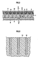
- hetero-semiconductor regions 15 made of p + type polysilicon corresponding to the p-type columnar structures can be formed as narrow regions at a time by trench etching, as illustrated in Fig. 3 showing the general configuration of the first embodiment.
- the p-type columnar structure can be greatly thinned (narrowed), although the horizontal width of an n-type columnar structure 14 (the drain region shown in Fig. 1) is about the same as those of the structures of earlier technology.
- a cell density of the overall element can be increased. The increase of the cell density permits a corresponding reduction in the on-resistance normalized according to the area of the element in the entire element.
- the first embodiment enables a size reduction of the region for holding the breakdown voltage of the element, and thus achieves an effect of reducing sufficiently the on-resistance normalized according to the area of the element.
- the first embodiment has an effect of achieving good breakdown voltage characteristics with little reverse leakage characteristics.
- the semiconductor device according to the first embodiment can contribute greatly to size and cost reductions of a power electronics system such as an inverter for motor drive.
- the semiconductor base substrate is made of any of silicon carbide (SiC) (employed herein), gallium nitride (GaN), or diamond.
- the hetero-semiconductor region 4 is made of at least one of monocrystalline silicon (silicon (Si)), polycrystalline silicon (employed herein), and amorphous silicon.
- Si silicon carbide
- GaN gallium nitride
- a general semiconductor material can be used to easily form the semiconductor device having a high breakdown voltage.
- the semiconductor device further includes the source electrode 8 formed on the first main surface of the semiconductor base substrate; and the drain electrode 9 formed on and connected ohmically with the second or the first main surface of the semiconductor base substrate (e.g., the second main surface because of the vertical device employed herein).
- the switching mechanism switches ON/OFF of a current between the drain electrode 9 and the source electrode 8, and the hetero-semiconductor region 4 is electrically connected to the source electrode 8. This allows realizing the power MOSFET, which constitutes the switching element having low on-resistance, at a low cost.
- the hetero-semiconductor region 4 is a second conductive type having a high concentration (e.g., the p type employed herein) with respect to the semiconductor base substrate. This allows realizing the switching element having low on-state resistance, at low cost.
- FIG. 2 is a sectional view showing a structure of an element portion of a semiconductor device according to the second embodiment of the present invention.
- the switching mechanism is applied to a U-gate (trench gate) power MOSFET.
- reference numerals 12 and 13 denote a gate insulating film and a U-gate electrode, respectively.
- the first embodiment has been described by referring to the sectional structure in which two base cells face each other.
- Fig. 2 showing the second embodiment, there is illustrated a wide range of the sectional structure in a way that a plurality of columnar hetero-semiconductor regions 4 made of p + type polysilicon are arranged.
- the other configurations and the basic operations, functions and effects of the second embodiment are equivalent to those of the first embodiment.
- the second embodiment facilitates forming the structure capable of obtaining SJ (RESURF (reduced surface field) effect) which exceeds the theoretical performance limits of SiC as in the case of the first embodiment.
- the second embodiment has a heterointerface, and therefore a low-on-resistance switch having good reverse recovery characteristics is realized.
- the hetero-semiconductor region 4 is formed to penetrate to the bottom of the n - type SiC drain region 1.
- the hetero-semiconductor region 4 does not necessarily reach the bottom of the n - type SiC drain region 1, or may reach into the n + type SiC substrate 2.
Landscapes
- Junction Field-Effect Transistors (AREA)
- Electrodes Of Semiconductors (AREA)
Abstract
Description
- The present invention relates to a semiconductor device and a method of manufacturing the same.
- Earlier techniques include a so-called superjunction (SJ) power MOSFET (metal oxide semiconductor field effect transistor) described in "Proceedings of 2004 International Symposium Power Semiconductor Devices & ICs, Kitakyushu, p. 459-462," for example.
- The SJ-MOSFET can exceed a limit of theoretical performance determined by an Si (silicon) material, although Si is used as the material of the SJ-MOSFET, Moreover, in the SJ-MOSFET, p and n impurity regions are formed in a sandwich arrangement in a drift region of a body portion. In this structure, a depletion layer is extended in a horizontal direction, and thereby it is possible to simultaneously deplete the whole drift region, which has not been possible with earlier structures. Therefore, the structure can achieve a higher impurity concentration in a p-type region and lower on-resistance as compared to the earlier structures.
- Because of needs of p-type and n-type columnar structures, the above-mentioned SJ structure has needed to form the p-type columnar structure on an n-type semiconductor substrate having a depth depending on an element breakdown voltage.
- Thus, formation of an element includes: a process of multistage epitaxial growth, and a process of impurity introduction on a patterned region after the epitaxial growth process. The processes are repeated multiple times to form the element. Thus, the SJ structure had a problem of rising costs.
- An object of the invention is to provide a semiconductor device capable of realizing a switching element having low on-resistance at a low cost, and a method of manufacturing a semiconductor device.
- In order to solve the foregoing problem, a semiconductor device of the invention includes a first conductive type semiconductor base substrate; and a switching mechanism which is formed on a first main surface of the semiconductor base substrate and switches ON/OFF of a current. In the semiconductor base substrate, a plurality of columnar hetero-semiconductor regions are formed at spaced intervals within the semiconductor substrate, and the hetero-semiconductor regions are made of a semiconductor material having a different band gap from the semiconductor substrate and extend between the first main surface and a second main surface opposite to the first main surface.
-
- Fig. 1 is a sectional view showing a structure of an element portion of a semiconductor device according to a first embodiment of the present invention;
- Fig. 2 is a sectional view showing a structure of an element portion of a semiconductor device according to a second embodiment of the present invention; and
- Fig. 3 is a sectional view showing a general structure of a heterojunction of the present invention.
- Embodiments of the present invention will be described in detail below with reference to the drawings. In the drawings to be described below, the same reference numerals designate parts having the same functions, and the repeated description of these parts will be omitted.
- A first embodiment of the invention will be described with reference to Fig. 1. Fig. 1 is a sectional view showing a structure of an element portion of a semiconductor device according to the first embodiment of the present invention.
- A configuration shown in Fig. 1 will be explained. A drain region 1 made of n- type SiC (silicon carbide) epitaxially grown is formed on an n+
type SiC substrate 2. A power MOSFET is formed on a first main surface of the n-type SiC drain region 1. A polytype of the SiC can be 4H, 6H, 3C, or others. Moreover, the SiC may be replaced by GaN (gallium nitride) or diamond, which is a wide band gap material excellent for use in a power device. - The power MOSFET used as a switching mechanism may be replaced by a switching mechanism of other switching devices. For example, a JFET (junction FET), a MESFET (metal-semiconductor FET), a bipolar transistor, or a switching mechanism utilizing a heterojunction, which is disclosed in Japanese Patent Laid-open Official Gazette
No. 2003-318398 type well region 3 and an n+type source region 5 are formed by double diffusion. Achannel region 10 is formed, on a surface of the p-type well region 3, in contact with the n+type source region 5, and immediately under the gate electrode 7. This switching mechanism controls an electric potential to be applied to the gate electrode 7, and thereby ON/OFF of a current between adrain electrode 9 and asource electrode 8 is switched. In other words, the switching mechanism in the case of the power MOSFET refers to the gate electrode 7, the gate insulating film 6, and thechannel region 10. In a case of the JFET, p-type well regions are formed with an n-type source region interposed therebetween. The p-type well region has a low concentration and a relatively great depth, and the n-type source region has a high concentration and a relatively shallow depth. The p-type well region constitutes a gate region, and a gate electrode is formed thereon. A region interposed in between the p-type well regions having a great depth constitutes a channel region. This switching mechanism controls an amount of injection of majority carriers from the n-type source region, by changing a height of a potential barrier across the channel region through application of gate and drain voltages. In other words, the switching mechanism in the case of the JFET refers to the gate electrode and the channel region. In the switching mechanism utilizing a heterojunction, a gate electrode is provided close to a heterojunction interface with a gate insulating film interposed therebetween. This switching mechanism controls a width of an energy barrier due to the heterojunction by controlling an electric potential to be applied to the gate electrode, and switches ON/OFF of a current by flowing a tunnel current. When GaN is used, a channel structure utilizing a two-dimensional electron gas cloud may be used. - As for the explanation of the power MOSFET, the n+
type source region 5 is formed within the p-type well region 3. The gate electrode 7 is formed on the gate insulating film 6 which is formed on the first main surface so as to lay on a plurality of (in Fig. 1, there are shown two p-type well regions 3) p-type well regions 3 arranged discretely. Thesource electrode 8 made of, for example, a metal is formed so as to connect to the n+type source region 5. Fig. 1 shows a representative example of an aspect in which two base unit cells face each other. A large number of cells, however, are actually connected in parallel. A concentration and a thickness of the drain region 1 are set according to a required breakdown voltage. The drain region 1 needs to have a thickness of about 10 µm as an example in order to obtain a breakdown voltage of 1000 V level. The n+type SiC substrate 2 is connected ohmically with thedrain electrode 9 on its rear surface. - The configuration of the first embodiment is characterized in that a hetero-
semiconductor region 4 made of p+ type polysilicon (polycrystalline silicon) is formed in a columnar shape in the drain region 1. The hetero-semiconductor region 4 made of the p+ type polysilicon is connected to thesource electrode 8 made of, for example, a metal. The hetero-semiconductor region 4 is at the same potential as thesource electrode 8, the n+type source region 5, and the p-type well region 3. - Next, a method of manufacturing the semiconductor device mentioned above will be described. Since a detailed method of manufacturing the power MOSFET portion is generally known, therefore the description of this portion will be omitted. The description will be given only with regard to a method of manufacturing an essential configuration of the present invention. The n- type drain region 1 is formed on the n+
type SiC substrate 2 by epitaxial growth. Atrench 11 is formed in the surface of the drain region 1 by trench etching. A p+ type polysilicon layer is deposited so as to fill in thetrench 11. After the completion of the deposition of the p+ type polysilicon layer in thetrench 11, the p+ type polysilicon layer deposited on the surface of the drain region 1 is removed by etch back or the like. Incidentally, introduction of p+ type impurities to the polysilicon layer can be performed simultaneously with or after the deposition of the polysilicon layer. As described above, the method of manufacturing a semiconductor device according to the first embodiment includes an operation of forming a plurality ofcolumnar trenches 11 in the first main surface of the semiconductor base substrate; and an operation of forming the hetero-semiconductor region 4 by filling each of thetrenches 11 with a semiconductor material (e.g., p+ type polysilicon) for forming the hetero-semiconductor region 4. The adoption of the above-mentioned manufacturing method facilitates a manufacturing process, and can prevent a rise in a manufacturing cost. Moreover, impurity implantation performed for each multistage epitaxial growth is not necessary. Thus, the above-mentioned manufacturing method can prevent variations in device characteristics and improve yields. Therefore, the manufacturing cost can be reduced. - The description will now be given with regard to an operation of the semiconductor device according to the first embodiment. The switching mechanism portion formed of the power MOSFET acts to switch ON/OFF of a main current passing through an element. In an operation of an original vertical power MOSFET, when the element turns on, a main current flows from the
drain electrode 9 to thesource electrode 8 through the n+type SiC substrate 2, the n- type drain region 1, thechannel region 10 formed immediately under the gate insulating film 6, and the n+type source region 5. When the element turns off, a reverse bias is applied to a heterojunction formed between the hetero-semiconductor region 4 and the n- type drain region 1. In this case, the hetero-semiconductor region 4 is made of p+ type polysilicon and is at the same potential as thesource electrode 8. The heterojunction serves as a diode having a high breakdown voltage. By experimental results obtained by inventors' tremendous effort, it has been found out that the p+ type is desirable to obtain diode characteristics which have a high breakdown voltage and produce little leakage current. - As described above, the semiconductor device according to the first embodiment includes the n+
type SiC substrate 2 and the n- type drain region 1 which constitute a first conductive type semiconductor base substrate; and the switching mechanism, which is formed on the first main surface of the semiconductor base substrate (e.g., the n- type drain region 1) and switches ON/OFF of a current. In the semiconductor device, a plurality of columnar hetero-semiconductor regions 4, which extend between the first main surface and a second main surface opposite to the first main surface, are formed at spaced intervals within the semiconductor base substrate (e.g., the n- type drain region 1). The hetero-semiconductor regions 4 are made of a semiconductor material (e.g., p+ type polysilicon) having a different band gap from the semiconductor base substrate (e.g., the n-type drain region 1). - By adopting the configuration of the first embodiment, a depletion layer can be extended in a horizontal direction in the drain region 1 when the element turns off. Therefore, the entire area of the drain region 1 is depleted, and a peak of electric field strength near an interface between the p-
type well region 3 and the drain region 1 is reduced. Accordingly, it is possible to impart a uniform distribution of electric field in a vertical direction. Since the peak of electric field strength is reduced, a breakdown voltage can be increased. Thereby, a concentration of the drain region 1 can be increased to reduce on-resistance. Therefore, the first embodiment can achieve both a high breakdown voltage and low on-resistance which exceed material limits (i.e., theoretical performance limits) of a wide band gap semiconductor such as SiC. The earlier technology previously mentioned has a problem as given below. In the p-type and the n-type columnar structures, a depletion layer is extended in a horizontal direction in a state where a reverse bias is applied to the element, and thereby it is necessary to ensure a sufficient horizontal dimension. Therefore, there has been a problem of an increase in the horizontal dimension of the overall element. In the element of the first embodiment, no depletion layer spreads in the hetero-semiconductor region 4 made of p+ type polysilicon, and thereby the p-type columnar structure can be formed as a narrow region. Therefore, the element of the first embodiment can be formed in a smaller horizontal dimension as compared to the SJ devices of earlier technology. As previously mentioned, the p-type columnar structure, which is formed between the n-type columnar structures (n-type drift regions) of the above-mentioned SJ device of earlier technology, has to introduce impurities for each multistage epitaxial growth. Thus, the SJ device of earlier technology inevitably has a great horizontal width in view of accuracy of alignment with patterning. On the other hand, in the first embodiment, hetero-semiconductor regions 15 made of p+ type polysilicon corresponding to the p-type columnar structures can be formed as narrow regions at a time by trench etching, as illustrated in Fig. 3 showing the general configuration of the first embodiment. Thus, the p-type columnar structure can be greatly thinned (narrowed), although the horizontal width of an n-type columnar structure 14 (the drain region shown in Fig. 1) is about the same as those of the structures of earlier technology. A cell density of the overall element can be increased. The increase of the cell density permits a corresponding reduction in the on-resistance normalized according to the area of the element in the entire element. As mentioned above, the first embodiment enables a size reduction of the region for holding the breakdown voltage of the element, and thus achieves an effect of reducing sufficiently the on-resistance normalized according to the area of the element. Moreover, the first embodiment has an effect of achieving good breakdown voltage characteristics with little reverse leakage characteristics. By the above-described effectiveness, the semiconductor device according to the first embodiment can contribute greatly to size and cost reductions of a power electronics system such as an inverter for motor drive. - The semiconductor base substrate is made of any of silicon carbide (SiC) (employed herein), gallium nitride (GaN), or diamond. The hetero-
semiconductor region 4 is made of at least one of monocrystalline silicon (silicon (Si)), polycrystalline silicon (employed herein), and amorphous silicon. Thus, a general semiconductor material can be used to easily form the semiconductor device having a high breakdown voltage. - The semiconductor device further includes the
source electrode 8 formed on the first main surface of the semiconductor base substrate; and thedrain electrode 9 formed on and connected ohmically with the second or the first main surface of the semiconductor base substrate (e.g., the second main surface because of the vertical device employed herein). In the semiconductor device, the switching mechanism switches ON/OFF of a current between thedrain electrode 9 and thesource electrode 8, and the hetero-semiconductor region 4 is electrically connected to thesource electrode 8. This allows realizing the power MOSFET, which constitutes the switching element having low on-resistance, at a low cost. - The hetero-
semiconductor region 4 is a second conductive type having a high concentration (e.g., the p type employed herein) with respect to the semiconductor base substrate. This allows realizing the switching element having low on-state resistance, at low cost. - A second embodiment of the present invention will be described with reference to Fig. 2. Fig. 2 is a sectional view showing a structure of an element portion of a semiconductor device according to the second embodiment of the present invention.
- In the second embodiment, the switching mechanism is applied to a U-gate (trench gate) power MOSFET. In Fig. 2,
reference numerals - The first embodiment has been described by referring to the sectional structure in which two base cells face each other. In Fig. 2 showing the second embodiment, there is illustrated a wide range of the sectional structure in a way that a plurality of columnar hetero-
semiconductor regions 4 made of p+ type polysilicon are arranged. The other configurations and the basic operations, functions and effects of the second embodiment are equivalent to those of the first embodiment. Specifically, the second embodiment facilitates forming the structure capable of obtaining SJ (RESURF (reduced surface field) effect) which exceeds the theoretical performance limits of SiC as in the case of the first embodiment. Moreover, the second embodiment has a heterointerface, and therefore a low-on-resistance switch having good reverse recovery characteristics is realized. - It should be noted that the above-described embodiments are for a purpose of facilitating the understanding of the present invention and are not intended to limit the present invention. Accordingly, each of the components disclosed in the aforementioned embodiments is intended to cover all such design changes and equivalences as fall within the technical scope of the present invention. Although the above-mentioned first and second embodiments have been described by giving the power MOSFET as an example of the switching mechanism, other switching mechanisms may be used, such as a JFET, a MESFET, a bipolar transistor, or a switching element utilizing a heterojunction disclosed in Japanese Patent Laid-open Official Gazette
No. 2003-318398 semiconductor region 4 is formed to penetrate to the bottom of the n- type SiC drain region 1. However, the hetero-semiconductor region 4 does not necessarily reach the bottom of the n- type SiC drain region 1, or may reach into the n+type SiC substrate 2. - The entire content of a Patent Application No. TOKUGAN 2004-349485 with a filing date of December 2, 2004 in Japan is hereby incorporated by reference.
- Although the invention is not limited to the embodiments described above. Modifications and variations of the embodiments described above will occur to those skilled in the art, in light of the teachings. The scope of the invention is defined with reference to the following claims.
Claims (5)
- A semiconductor device, comprising:a first conductive type semiconductor base substrate (1, 2); anda switching mechanism (6, 7, 10) which is formed on a first main surface of the semiconductor base substrate (1, 2) and switches ON/OFF of a current,wherein a plurality of columnar hetero-semiconductor regions (4), which are made of a semiconductor material having a different band gap from the semiconductor base substrate (1, 2), are formed at spaced intervals within the semiconductor base substrate (1, 2), and the hetero-samiconductor regions (4) extend between the first main surface and a second main surface opposite to the first main surface.
- The semiconductor device according to claim 1, wherein the semiconductor base substrate (1, 2) is made of any one of silicon carbide (SiC), gallium nitride (GaN), and diamond, and the hetero-semiconductor regions (4) are made of at least one of single crystal silicon, polycrystalline silicon, and amorphous silicon.
- The semiconductor device according to any one of claims 1 and 2, further comprising:a source electrode (8) formed on the first main surface of the semiconductor base substrate (1, 2); anda drain electrode (9) formed on and connected ohmically with the second or the first main surface of the semiconductor base substrate (1, 2),
wherein the switching mechanism (6, 7, 10) switches ON/OFF of a current between the drain electrode (9) and the source electrode (8), and the hetero-semiconductor regions (4) are electrically connected to the source electrode (8). - The semiconductor device according to any one of claims 2 and 3,
wherein the hetero-semiconductor regions (4) are a second conductive type having a high concentration with respect to the semiconductor base substrate (1, 2). - A method of manufacturing a semiconductor device according to any one of claims 1 to 4, comprising:forming a plurality of columnar trenches (11) in the first main surface of the semiconductor base substrate (1, 2); andforming the hetero-semiconductor regions (4) by filling each of the trenches with the semiconductor material.
Priority Applications (1)
| Application Number | Priority Date | Filing Date | Title |
|---|---|---|---|
| EP06011118.4A EP1863096B1 (en) | 2006-05-30 | 2006-05-30 | Semiconductor device and method of manufacturing the same |
Applications Claiming Priority (1)
| Application Number | Priority Date | Filing Date | Title |
|---|---|---|---|
| EP06011118.4A EP1863096B1 (en) | 2006-05-30 | 2006-05-30 | Semiconductor device and method of manufacturing the same |
Publications (2)
| Publication Number | Publication Date |
|---|---|
| EP1863096A1 true EP1863096A1 (en) | 2007-12-05 |
| EP1863096B1 EP1863096B1 (en) | 2017-07-19 |
Family
ID=37000177
Family Applications (1)
| Application Number | Title | Priority Date | Filing Date |
|---|---|---|---|
| EP06011118.4A Ceased EP1863096B1 (en) | 2006-05-30 | 2006-05-30 | Semiconductor device and method of manufacturing the same |
Country Status (1)
| Country | Link |
|---|---|
| EP (1) | EP1863096B1 (en) |
Cited By (5)
| Publication number | Priority date | Publication date | Assignee | Title |
|---|---|---|---|---|
| CN109119463A (en) * | 2018-08-29 | 2019-01-01 | 电子科技大学 | A kind of lateral trench type MOSFET element and preparation method thereof |
| CN109192780A (en) * | 2018-08-29 | 2019-01-11 | 电子科技大学 | A kind of lateral MOSFET device and preparation method thereof |
| WO2019101685A1 (en) * | 2017-11-23 | 2019-05-31 | Robert Bosch Gmbh | Vertical power transistor with heterojunctions |
| CN110429137A (en) * | 2019-08-15 | 2019-11-08 | 西安电子科技大学 | VDMOS with partial gallium nitride/silicon semiconductor material heterojunction and its manufacturing method |
| CN110518069A (en) * | 2019-08-15 | 2019-11-29 | 西安电子科技大学 | With partially carbonized silicon/silicon semiconductor material hetero-junctions VDMOS and preparation method thereof |
Citations (4)
| Publication number | Priority date | Publication date | Assignee | Title |
|---|---|---|---|---|
| US5216275A (en) * | 1991-03-19 | 1993-06-01 | University Of Electronic Science And Technology Of China | Semiconductor power devices with alternating conductivity type high-voltage breakdown regions |
| DE19839970A1 (en) * | 1998-09-02 | 2000-03-16 | Siemens Ag | Edge structure and drift region, e.g. for a junction-trench MOSFET, diode, IGBT or silicon carbide JFET, comprises multilevel embedded regions which are connected below active zones and are floating elsewhere |
| EP1139433A1 (en) * | 2000-03-31 | 2001-10-04 | Shindengen Electric Manufacturing Company, Limited | Semiconductor device having a Schottky barrier diode structure |
| EP1544920A2 (en) * | 2003-12-18 | 2005-06-22 | Nissan Motor Co., Ltd. | Semiconductor device having a heterojunction or a Schottky junction |
Family Cites Families (1)
| Publication number | Priority date | Publication date | Assignee | Title |
|---|---|---|---|---|
| JP4265201B2 (en) * | 2002-10-25 | 2009-05-20 | 富士電機デバイステクノロジー株式会社 | Super junction semiconductor device |
-
2006
- 2006-05-30 EP EP06011118.4A patent/EP1863096B1/en not_active Ceased
Patent Citations (4)
| Publication number | Priority date | Publication date | Assignee | Title |
|---|---|---|---|---|
| US5216275A (en) * | 1991-03-19 | 1993-06-01 | University Of Electronic Science And Technology Of China | Semiconductor power devices with alternating conductivity type high-voltage breakdown regions |
| DE19839970A1 (en) * | 1998-09-02 | 2000-03-16 | Siemens Ag | Edge structure and drift region, e.g. for a junction-trench MOSFET, diode, IGBT or silicon carbide JFET, comprises multilevel embedded regions which are connected below active zones and are floating elsewhere |
| EP1139433A1 (en) * | 2000-03-31 | 2001-10-04 | Shindengen Electric Manufacturing Company, Limited | Semiconductor device having a Schottky barrier diode structure |
| EP1544920A2 (en) * | 2003-12-18 | 2005-06-22 | Nissan Motor Co., Ltd. | Semiconductor device having a heterojunction or a Schottky junction |
Non-Patent Citations (1)
| Title |
|---|
| HAJJIAH A T ET AL: "Novel SiC-trench-MOSFET with reduced oxide electric field", SOLID-STATE AND INTEGRATED CIRCUITS TECHNOLOGY, 2004, PROCEEDINGS, 18 October 2004 (2004-10-18), pages 340 - 344, XP010805392 * |
Cited By (8)
| Publication number | Priority date | Publication date | Assignee | Title |
|---|---|---|---|---|
| WO2019101685A1 (en) * | 2017-11-23 | 2019-05-31 | Robert Bosch Gmbh | Vertical power transistor with heterojunctions |
| CN109119463A (en) * | 2018-08-29 | 2019-01-01 | 电子科技大学 | A kind of lateral trench type MOSFET element and preparation method thereof |
| CN109192780A (en) * | 2018-08-29 | 2019-01-11 | 电子科技大学 | A kind of lateral MOSFET device and preparation method thereof |
| CN109119463B (en) * | 2018-08-29 | 2020-07-31 | 电子科技大学 | A kind of lateral trench type MOSFET device and preparation method thereof |
| CN109192780B (en) * | 2018-08-29 | 2020-11-27 | 电子科技大学 | A kind of lateral MOSFET device and preparation method thereof |
| CN110429137A (en) * | 2019-08-15 | 2019-11-08 | 西安电子科技大学 | VDMOS with partial gallium nitride/silicon semiconductor material heterojunction and its manufacturing method |
| CN110518069A (en) * | 2019-08-15 | 2019-11-29 | 西安电子科技大学 | With partially carbonized silicon/silicon semiconductor material hetero-junctions VDMOS and preparation method thereof |
| CN110518069B (en) * | 2019-08-15 | 2020-10-13 | 西安电子科技大学 | VDMOS with partial silicon carbide/silicon semiconductor material heterojunction and method of making the same |
Also Published As
| Publication number | Publication date |
|---|---|
| EP1863096B1 (en) | 2017-07-19 |
Similar Documents
| Publication | Publication Date | Title |
|---|---|---|
| JP7658394B2 (en) | Semiconductor Device | |
| EP1204145B1 (en) | Semiconductor element | |
| US11961904B2 (en) | Semiconductor device including trench gate structure and buried shielding region and method of manufacturing | |
| US7436004B2 (en) | Semiconductor device | |
| JP3385938B2 (en) | Silicon carbide semiconductor device and method of manufacturing the same | |
| JP7697777B2 (en) | Trench-gate silicon carbide devices | |
| EP1503425B1 (en) | Heterojunction semiconductor device and method of manufacturing the same | |
| US7479678B2 (en) | Semiconductor element and method of manufacturing the same | |
| US20170213908A1 (en) | Self-aligned shielded-gate trench mos-controlled silicon carbide switch with reduced miller capacitance and method of manufacturing the same | |
| CA2567070A1 (en) | Silicon carbide devices and fabricating methods therefor | |
| CN107210318A (en) | High-voltage semi-conductor equipment | |
| US12176423B2 (en) | FinFET power semiconductor devices | |
| JP2005011846A (en) | Semiconductor device | |
| US7521731B2 (en) | Semiconductor device and method of manufacturing the same | |
| EP1575097A2 (en) | Semiconductor device with heterojunction | |
| EP1863096B1 (en) | Semiconductor device and method of manufacturing the same | |
| CN100561739C (en) | Semiconductor device | |
| JP5614399B2 (en) | Field effect transistor and manufacturing method thereof | |
| CN101083280B (en) | Semiconductor device and method of manufacturing same | |
| KR100766668B1 (en) | Semiconductor device and manufacturing method thereof | |
| JP7628874B2 (en) | Semiconductor device and its manufacturing method | |
| GB2548126A (en) | A SiC trench transistor | |
| CN121909753A (en) | silicon carbide semiconductor devices |
Legal Events
| Date | Code | Title | Description |
|---|---|---|---|
| PUAI | Public reference made under article 153(3) epc to a published international application that has entered the european phase |
Free format text: ORIGINAL CODE: 0009012 |
|
| 17P | Request for examination filed |
Effective date: 20060530 |
|
| AK | Designated contracting states |
Kind code of ref document: A1 Designated state(s): AT BE BG CH CY CZ DE DK EE ES FI FR GB GR HU IE IS IT LI LT LU LV MC NL PL PT RO SE SI SK TR |
|
| AX | Request for extension of the european patent |
Extension state: AL BA HR MK YU |
|
| AKX | Designation fees paid |
Designated state(s): DE FR GB |
|
| 17Q | First examination report despatched |
Effective date: 20090126 |
|
| APBK | Appeal reference recorded |
Free format text: ORIGINAL CODE: EPIDOSNREFNE |
|
| APBN | Date of receipt of notice of appeal recorded |
Free format text: ORIGINAL CODE: EPIDOSNNOA2E |
|
| APBR | Date of receipt of statement of grounds of appeal recorded |
Free format text: ORIGINAL CODE: EPIDOSNNOA3E |
|
| APAF | Appeal reference modified |
Free format text: ORIGINAL CODE: EPIDOSCREFNE |
|
| APBX | Invitation to file observations in appeal sent |
Free format text: ORIGINAL CODE: EPIDOSNOBA2E |
|
| APBZ | Receipt of observations in appeal recorded |
Free format text: ORIGINAL CODE: EPIDOSNOBA4E |
|
| APBT | Appeal procedure closed |
Free format text: ORIGINAL CODE: EPIDOSNNOA9E |
|
| GRAP | Despatch of communication of intention to grant a patent |
Free format text: ORIGINAL CODE: EPIDOSNIGR1 |
|
| INTG | Intention to grant announced |
Effective date: 20170407 |
|
| GRAS | Grant fee paid |
Free format text: ORIGINAL CODE: EPIDOSNIGR3 |
|
| GRAA | (expected) grant |
Free format text: ORIGINAL CODE: 0009210 |
|
| AK | Designated contracting states |
Kind code of ref document: B1 Designated state(s): DE FR GB |
|
| REG | Reference to a national code |
Ref country code: GB Ref legal event code: FG4D |
|
| REG | Reference to a national code |
Ref country code: DE Ref legal event code: R096 Ref document number: 602006053043 Country of ref document: DE |
|
| REG | Reference to a national code |
Ref country code: FR Ref legal event code: PLFP Year of fee payment: 13 |
|
| REG | Reference to a national code |
Ref country code: DE Ref legal event code: R097 Ref document number: 602006053043 Country of ref document: DE |
|
| PLBE | No opposition filed within time limit |
Free format text: ORIGINAL CODE: 0009261 |
|
| STAA | Information on the status of an ep patent application or granted ep patent |
Free format text: STATUS: NO OPPOSITION FILED WITHIN TIME LIMIT |
|
| 26N | No opposition filed |
Effective date: 20180420 |
|
| PGFP | Annual fee paid to national office [announced via postgrant information from national office to epo] |
Ref country code: FR Payment date: 20230420 Year of fee payment: 18 Ref country code: DE Payment date: 20230419 Year of fee payment: 18 |
|
| PGFP | Annual fee paid to national office [announced via postgrant information from national office to epo] |
Ref country code: GB Payment date: 20230420 Year of fee payment: 18 |
|
| REG | Reference to a national code |
Ref country code: DE Ref legal event code: R079 Ref document number: 602006053043 Country of ref document: DE Free format text: PREVIOUS MAIN CLASS: H01L0029060000 Ipc: H10D0062100000 |
|
| REG | Reference to a national code |
Ref country code: DE Ref legal event code: R119 Ref document number: 602006053043 Country of ref document: DE |
|
| GBPC | Gb: european patent ceased through non-payment of renewal fee |
Effective date: 20240530 |
|
| PG25 | Lapsed in a contracting state [announced via postgrant information from national office to epo] |
Ref country code: DE Free format text: LAPSE BECAUSE OF NON-PAYMENT OF DUE FEES Effective date: 20241203 |
|
| PG25 | Lapsed in a contracting state [announced via postgrant information from national office to epo] |
Ref country code: FR Free format text: LAPSE BECAUSE OF NON-PAYMENT OF DUE FEES Effective date: 20240531 |
|
| PG25 | Lapsed in a contracting state [announced via postgrant information from national office to epo] |
Ref country code: GB Free format text: LAPSE BECAUSE OF NON-PAYMENT OF DUE FEES Effective date: 20240530 |