EP1863088A2 - FET semiconductor device with partial annular gate electrodes - Google Patents
FET semiconductor device with partial annular gate electrodes Download PDFInfo
- Publication number
- EP1863088A2 EP1863088A2 EP07010724A EP07010724A EP1863088A2 EP 1863088 A2 EP1863088 A2 EP 1863088A2 EP 07010724 A EP07010724 A EP 07010724A EP 07010724 A EP07010724 A EP 07010724A EP 1863088 A2 EP1863088 A2 EP 1863088A2
- Authority
- EP
- European Patent Office
- Prior art keywords
- semiconductor device
- field effect
- fet
- fets
- effect transistors
- Prior art date
- Legal status (The legal status is an assumption and is not a legal conclusion. Google has not performed a legal analysis and makes no representation as to the accuracy of the status listed.)
- Withdrawn
Links
Images







Classifications
-
- H—ELECTRICITY
- H10—SEMICONDUCTOR DEVICES; ELECTRIC SOLID-STATE DEVICES NOT OTHERWISE PROVIDED FOR
- H10D—INORGANIC ELECTRIC SEMICONDUCTOR DEVICES
- H10D84/00—Integrated devices formed in or on semiconductor substrates that comprise only semiconducting layers, e.g. on Si wafers or on GaAs-on-Si wafers
- H10D84/80—Integrated devices formed in or on semiconductor substrates that comprise only semiconducting layers, e.g. on Si wafers or on GaAs-on-Si wafers characterised by the integration of at least one component covered by groups H10D12/00 or H10D30/00, e.g. integration of IGFETs
- H10D84/82—Integrated devices formed in or on semiconductor substrates that comprise only semiconducting layers, e.g. on Si wafers or on GaAs-on-Si wafers characterised by the integration of at least one component covered by groups H10D12/00 or H10D30/00, e.g. integration of IGFETs of only field-effect components
- H10D84/83—Integrated devices formed in or on semiconductor substrates that comprise only semiconducting layers, e.g. on Si wafers or on GaAs-on-Si wafers characterised by the integration of at least one component covered by groups H10D12/00 or H10D30/00, e.g. integration of IGFETs of only field-effect components of only insulated-gate FETs [IGFET]
-
- H—ELECTRICITY
- H10—SEMICONDUCTOR DEVICES; ELECTRIC SOLID-STATE DEVICES NOT OTHERWISE PROVIDED FOR
- H10D—INORGANIC ELECTRIC SEMICONDUCTOR DEVICES
- H10D89/00—Aspects of integrated devices not covered by groups H10D84/00 - H10D88/00
- H10D89/10—Integrated device layouts
-
- H—ELECTRICITY
- H10—SEMICONDUCTOR DEVICES; ELECTRIC SOLID-STATE DEVICES NOT OTHERWISE PROVIDED FOR
- H10D—INORGANIC ELECTRIC SEMICONDUCTOR DEVICES
- H10D84/00—Integrated devices formed in or on semiconductor substrates that comprise only semiconducting layers, e.g. on Si wafers or on GaAs-on-Si wafers
- H10D84/80—Integrated devices formed in or on semiconductor substrates that comprise only semiconducting layers, e.g. on Si wafers or on GaAs-on-Si wafers characterised by the integration of at least one component covered by groups H10D12/00 or H10D30/00, e.g. integration of IGFETs
- H10D84/82—Integrated devices formed in or on semiconductor substrates that comprise only semiconducting layers, e.g. on Si wafers or on GaAs-on-Si wafers characterised by the integration of at least one component covered by groups H10D12/00 or H10D30/00, e.g. integration of IGFETs of only field-effect components
- H10D84/83—Integrated devices formed in or on semiconductor substrates that comprise only semiconducting layers, e.g. on Si wafers or on GaAs-on-Si wafers characterised by the integration of at least one component covered by groups H10D12/00 or H10D30/00, e.g. integration of IGFETs of only field-effect components of only insulated-gate FETs [IGFET]
- H10D84/83125—Integrated devices formed in or on semiconductor substrates that comprise only semiconducting layers, e.g. on Si wafers or on GaAs-on-Si wafers characterised by the integration of at least one component covered by groups H10D12/00 or H10D30/00, e.g. integration of IGFETs of only field-effect components of only insulated-gate FETs [IGFET] the IGFETs characterised by having shared source or drain regions
Definitions
- the present invention relates to a semiconductor device.
- FETs field effect transistors
- higher pair accuracy or namely higher relativity accuracy is often required between those FETs.
- high pair accuracy is required for reducing an input off-set voltage for such operational amplifier or such comparator.
- Typical conventional semiconductor devices provided with a plurality of FETs include semiconductor devices described in Japanese Patent Laid-Open No. S62-81054 ( No. 1987-81054 ) and Japanese Patent Laid-Open No. H06-13574 ( No. 1994-13574 ).
- FIG. 16 is a plan view, showing a semiconductor device described in Japanese Patent Laid-Open No. S62-81054 .
- a semiconductor device 100 includes four FETs 101, 102, 103 and 104. Each of these FETs has an annular gate electrode 111, and a source electrode 112 and a drain region 113 provided in the outside and the inside thereof, respectively.
- the source electrode, the gate electrode and the drain electrode are electrically coupled with each other.
- a coupling situation between the FET 102 and the FET 104 is similar to that between the FET 101 and the FET 103.
- a combination of the FET 101 and the FET 103 substantially functions as one FET and a combination of the FET 102 and the FET 104 substantially functions as another FET. Then, the FET composed of the FETs 101 and 103 and the FET composed of the FETs 102 and 104 constitute an FET pair.
- Fig. 17 is a plan view, showing a semiconductor device described in Japanese Patent Laid-Open No. H06-13574 .
- a semiconductor device 200 an FET 210a and an FET 210b constituting an FET pair are also provided.
- the FETs 210a and 210b share a source region 201.
- the FET 210a has a gate electrode 202a and a drain region 203a.
- the FET 210b has a gate electrode 202b and a drain region 203b.
- the FETs 101,102,103 and 104 are disposed to be spaced apart from each other.
- the pair accuracies of the FET-pairs composed of such FETs are more easily affected by a variation of impurity concentration in the diffusion layer in the substrate surface, as compared with the configuration, in which these are disposed closely with each other.
- geometries of the respective gate electrodes 202a and 202b are equivalent to a partial rectangular (more specifically, three in four sides that constitutes a rectangle). Therefore, channel-length in corners of the gate electrode 202a and 202b (for example, a section surrounded with dotted line L1) is different from that of other sections. Since an electric current flowing through the source and the drain tends to flow through a pass of shorter channel-length as possible, a deviation is created in such electric current. This cause being susceptive with an influence of a variation of an impurity concentration in the diffusion layer in the substrate surface, leading to a decrease in the pair accuracy of the FET-pair.
- a semiconductor device comprising: a plurality of field effect transistors provided in a certain region defined by an element isolation region, wherein gate electrodes of the plurality of field effect transistors are arranged along a circle in plan view, and wherein at least two field effect transistors selected from the plurality of field effect transistors have substantially same geometry.
- a plurality of FETs are provided in a certain region.
- these FETs are more easily arranged to be closer to each other, as compared with a case of providing the FETs in different certain regions, respectively. Therefore, the pair accuracy of the FET-pair composed of these FETs is difficult to be influenced by a variation of an impurity concentration in the diffusion layer in the substrate surface.
- the gate electrodes of the FETs are arranged along a circle. Thus, unlikely with the semiconductor device shown in Fig. 17, a deviation in an electric current flowing through the source and the drain can be prevented.
- a semiconductor device having a constitution that is suitable in improving a pair accuracy of an FET-pair is achieved.
- Fig. 1 is a plan view, showing first embodiment of a semiconductor device according to the present invention.
- a semiconductor device 1 includes an FET 10 (first FET), an FET 20 (second FET), an FET 30 (third FET) and an FET 40 (fourth FET). These FETs 10, 20, 30 and 40 are provided in an active region R1 (certain region).
- the active region means a region defined by an element isolation region, as described above. More specifically, the active region R1 is surrounded by an element isolation region (not shown in Fig. 1). In addition, no element isolation region is present in the active region R1.
- the FET 10, the FET 20, the FET 30 and the FET 40 have a gate electrode 12, a gate electrode 22, a gate electrode 32 and a gate electrode 42, respectively.
- the gate electrode 12, the gate electrode 22, the gate electrode 32 and the gate electrode 42 are arranged along a circle in this sequence in plan view.
- Materials of the gate electrodes 12, 22, 32 and 42 are, for example, polysilicon.
- the FETs 10, 20, 30 and 40 have a substantially identical geometry. Therefore, the gate electrodes 12, 22, 32 and 42 also have a substantially identical geometry.
- the term "to have a substantially identical geometry” means that geometries thereof in plan view are geometrically congruence. More specifically, as shown in Fig.
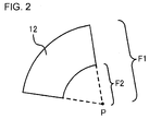
- each of the gate electrodes 12, 22, 32 and 42 has a geometry that is substantially equivalent to a partial annular circle, which is prepared by eliminating a second sector F2 from a first sector F1 in plan view, the first sector F1 having a center P, which is equivalent to a center of the aforementioned circle, and the second sector having the center P, which is also equivalent to the center of the aforementioned circle, and having a radius, which is shorter than a radius of the first sector F1.
- the exemplary implementation is made in reference to the gate electrode 12.
- the outside of the above-described circle in plan view, or in other words, the outside of the gate electrode 12, 22, 32 and 42 are provided with diffusion layers 14, 24, 34 and 44 (first diffusion layer).
- the diffusion layer 44 with the gate electrode 42 and the diffusion layer 56 constitute the FET 40.
- the diffusion layers 14, 24, 34 and 44 function as drain regions of the FETs 10, 20, 30 and 40, respectively.
- the inside of the above-described circle in plan view is, or in other words, the insides of the gate electrodes 12, 22, 32 and 42 are, provided with the diffusion layer 56 (second diffusion layer).
- the diffusion layer 56 is shared by the FETs 10, 20, 30 and 40.
- the diffusion layer 56 functions as source regions of the FETs 10, 20, 30 and 40.
- the source region (diffusion layer 56), the gate electrode 32 and the drain region (diffusion layer 34) of the FET 30 are electrically coupled to the source region (diffusion layer 56), the gate electrode 12 and the drain region (diffusion layer 14) of the FET 10, respectively.
- the source region (diffusion layer 56), the gate electrode 42 and the drain region (diffusion layer 44) of the FET 40 are electrically coupled to the source region (diffusion layer 56), the gate electrode 22 and the drain region (diffusion layer 24) of the FET 20, respectively.
- one combination of the FET 10 and the FET 30 substantially function as an FET
- another combination of the FET 20 and the FET 40 substantially function as another FET.
- an FET pair is constituted of the FET, which is composed of the FETs 10 and 30, and the FET, which is composed of from FET 20 and 40.
- Fig. 3A and Fig. 3B are cross-sectional views, showing cross sections along line III-III of the semiconductor device 1 of Fig. 1.
- Fig. 4A and Fig. 4B are cross-sectional views, showing cross sections along line IV-IV of the semiconductor device 1 of Fig. 1.
- Fig. 3A and Fig. 4A represent N-channel FETs 10, 20, 30 and 40
- Fig. 3B and Fig. 4B represent P-channel FETs 10, 20, 30 and 40.
- the above-described gate electrodes 12, 22, 32 and 42 are formed on a semiconductor substrate 61.
- the diffusion layers 14, 24, 34 and 44 and the diffusion layer 56 are formed in the semiconductor substrate 61.
- the diffusion layers 14, 24, 34 and 44 and the diffusion layer 56 are N+ type when the FETs 10, 20, 30 and 40 are N-channel type FETs, and are P+ type when the FETs 10, 20, 30 and 40 are P-channel type FETs.
- the semiconductor substrate 61 includes an N-type substrate 62 and an N-type epitaxial layer 64 formed thereon. However, it is not essential to provide the epitaxial layer 64 in the semiconductor substrate 61.
- a P-type well region 66 is further formed in a surface layer of the semiconductor substrate 61.
- the semiconductor substrate 61 is provided with an element isolation region 68 formed therein. Typical configuration of the element isolation region 68 includes shallow trench isolation (STI) or local oxidation of silicon (LOCOS).
- STI shallow trench isolation
- LOCS local oxidation of silicon
- An interlayer insulating film 72 is also provided on the semiconductor substrate 61. Further, the source electrode 57 is coupled to the diffusion layer 56 via an opening formed in the interlayer insulating film 72, and, the drain electrode 15 and the drain electrode 35 are coupled to the diffusion layer 14 and the diffusion layer 34, respectively. In addition to above, the diffusion layers 24 and 44, which do not appear in the cross-sectional view of Fig. 4A or Fig. 4B, are coupled to the drain electrodes, similarly as the diffusion layer 14 and 34. Further, the interlayer insulating film 72, the source electrode 57 and the drain electrode 15 and 35 are not shown in the plan view of Fig. 1.
- Fig. 5 and Fig. 6 are circuit architecture diagrams, showing a general comparator.
- a comparator presented in these diagrams includes a differential circuit 82 and a mirror circuit 84.
- the differential circuit 82 is constituted of an FET pair, which is composed of two N-channel FETs (MN1 and MN2) in the exemplary implementation shown in Fig. 5, and is alternatively constituted of an FET pair, which is composed of two P-channel FETs (MP3 and MP4) in the exemplary implementation shown in Fig. 6.
- the mirror circuit 84 is constituted of an FET pair, which is composed of two P-channel FETs (MP1 and MP2) in the exemplary implementation shown in Fig. 5, and is alternatively constituted of an FET pair, which is composed of two N-channel FETs (MN3 and MN4) in the exemplary implementation shown in Fig. 6.
- FET pair which is composed of two P-channel FETs (MP1 and MP2) in the exemplary implementation shown in Fig. 5
- MN3 and MN4 N-channel FETs
- sources of FETs are represented by SP1, SP2, SN1 and SN2
- gates of FETs are represented by GP1, GP2, GN1 and GN2
- drains of FETs are represented by DP1, DP2, DN1 and DN2, respectively.
- sources of FETs are represented by SP3, SP4, SN3 and SN4, gates of FETs (MP3, MP4, MN3 and MN4) are represented by GP3, GP4, GN3 and GN4, and drains of FETs (MP3, MP4, MN3 and MN4) are represented by DP3, DP4, DN3 and DN4, respectively.
- the present invention may be preferably applied to the comparator having such configuration.
- the FET composed of the FETs 20 and 40 may be employed for the MN1 (or MP3), and the FET composed of the FETs 10 and 30 may be employed for the MN2 (or MP4).
- Similar configuration may be applied to the mirror circuit 84, and specifically, the FET composed of the FETs 10 and 30 may be employed for the MP1 (or MN3), and the FET composed of the FETs 20 and 40 may be employed for the MP2 (or MN4).
- Fig. 7 is a plan view, showing an example of a circuit layout in a case of applying the present invention to the comparator of Fig. 5.
- a differential circuit (differential circuit 82 of Fig. 5) is disposed in an active region R1 in an upper section of the diagram
- a mirror circuit (mirror circuit 84 of Fig. 5) is disposed in an active region R1 in a lower section of the diagram.
- the FETs 10 and 30 correspond to the MN2 of Fig. 5
- the FETs 20 and 40 correspond to the MN1.
- the FETs 10 and 30 correspond to the MP1 of Fig. 5
- the FETs 20 and 40 correspond to the MP2.
- the respective gate electrodes of the FETs (MP1 and MP2) are mutually coupled via a metallic interconnect 94.
- a numeral 92 in Fig. 7 represents a polysilicon.
- an improved pair accuracy of the FET pair (NM1 and MN2) of the differential circuit 82 allows a reduced input off-set voltage of the comparator.
- an improved pair accuracy of the FET pair (NP1 and MP2) of the mirror circuit 84 allows a reduced input off-set voltage of the comparator.
- the FETs 10, 20, 30 and 40 are provided in one active region R1.
- the pair accuracy of the FET pair composed of these FETs is difficult to be influenced by a variation of an impurity concentration in the diffusion layer in the substrate surface.
- the gate electrodes 12, 22, 32 and 42 of the FETs are arranged along one circle. Therefore, unlike as a case of the semiconductor device shown in Fig. 17, no corner of the gate electrode is present on the channel-forming region.
- the channel-lengths of respective FETs 10, 20, 30 and 40 are substantially constant, thereby preventing an electric current flowing through the source and the drain from being unevenly distributed. Therefore, the semiconductor device 1 having the structure suitable in improving the pair accuracy of the FET pair can be achieved.
- the FETs 10, 20, 30 and 40 are provided in the same active region R1, an area occupied by these FETs can be reduced. This eventually contributes to a miniaturization of the semiconductor device 1. On the contrary, when a plurality of FETs are provided in separate active regions as shown by the semiconductor device in Fig. 16, an area occupied by these FETs is increased.
- the pair accuracy of the FET pair can be provided if the FETs 10 and 20 have substantially an identical geometry and the FETs 30 and 40 have substantially an identical geometry which is different from the identical geometry of the FETs 10 and 20.
- This allows an improved pair accuracy of the FET pair constituted of the FETs 10 and 30 and the FETs 20 and 40.
- the FETs 10, 20, 30 and 40 have substantially an identical geometry, which allows further improvement in the pair accuracy of the FET pair.
- the FET pair having different geometries are easily affected by a dimension difference, resulting in providing a structure that is not suited for providing an improved pair accuracy.
- Fig. 18 is a plan view, showing a conventional semiconductor device comprising a plurality of FETs having different geometries.
- the semiconductor device 300 is described in Japanese Patent Laid-Open No. S62-81054 , similarly as the semiconductor device of Fig. 16.
- a gate electrode 311a and a gate electrode 311b are provided in the semiconductor device 300.
- the gate electrodes 311a and 311b have different geometries.
- the gate electrode 311a with the source electrode 312a constitute an FET.
- the gate electrode 311b, with_the source electrode 312b constitute another FET.
- These two FETs share a drain electrode 313. Since the semiconductor device 300 is easily affected by a dimension difference, resulting in a deteriorated dimensional accuracy, it is difficult to control an area ratio of the channel-forming regions of two FETs with higher accuracy.
- the geometries of the respective gate electrodes 12, 22, 32 and 42 are substantially equivalent to a partial annular circle, which is prepared by eliminating a second sector F2 from a first sector F1. This allows easily achieving the FETs having a constant channel-length.
- a combination of the FET 10 and the FET 30 substantially function as an FET
- another combination of the FET 20 and the FET 40 substantially function as another FET.
- an impurity concentration is lower as closer to the right end in the diagram of Fig. 1
- the diffusion layers of the FET 10 and the FET 40 have relatively higher concentrations
- the diffusion layers of the FET 20 and the FET 30 have relatively lower concentrations.
- the diffusion layer 56 is shared by the FETs 10, 20, 30 and 40.
- a plurality of FETs having the source regions that are mutually electrically coupled with a simple configuration can be obtained.
- this preferably allows applying the semiconductor device 1 to circuits such as a differential circuit or a mirror circuit, employing the FET pair having source regions that are mutually coupled.
- a differential circuit or a mirror circuit employing the FET pair having source regions that are mutually coupled.
- an input off-set voltage of the comparator can be reduced.
- Fig. 8 is a plan view, showing second embodiment of a semiconductor device according to the present invention.
- a semiconductor device 2 the configurations of the gate electrodes 12, 22, 32 and 42 are different from that of the semiconductor device 1 described in reference to Fig. 1.
- Other configurations of the semiconductor device 2 are similar to that of the semiconductor device 1.
- an end portion 12a of a gate electrode 12 protrudes toward the outside of the above-described circle.
- the protruded section defines an end portion of a diffusion layer 14.
- Such protruded section extends to the outside of an active region R1. This provides the diffusion layer 14 being completely surrounded by the gate electrode 12 and an element isolation region, in plan view.
- the configurations of the gate electrodes 22, 32 and 42 are also similar to the gate electrode 12.
- the semiconductor device 2 is compared with the semiconductor device 1.
- the exemplary implementation will be made in reference to the FET 10.
- a dimensional accuracy of the channel-forming region depends upon three parameters, namely: a dimensional accuracy in the geometry of the gate electrode 12 (polysilicon, for example); a dimensional accuracy in the geometry of the diffusion layer 14; and a dimensional accuracy in the geometry of the diffusion layer 56.
- a dimensional accuracy of the channel-forming region depends upon two parameters, namely: a dimensional accuracy in the geometry of the gate electrode 12; and a dimensional accuracy in the geometry of the diffusion layer 56. Therefore, according to the semiconductor device 2, more improved pair accuracy of the FET pair can be achieved, as compared with the semiconductor device 1.
- Other advantageous effects of the semiconductor device 2 are similar to that of the semiconductor device 1.
- Fig. 9 is a plan view, showing third embodiment of a semiconductor device according to the present invention.
- a semiconductor device 3 the configurations of the gate electrodes 12, 22, 32 and 42 are different from that of the semiconductor device 1 described in reference to Fig. 1.
- Other configurations of the semiconductor device 3 are similar to that of the semiconductor device 1.
- an end portion 12a of a gate electrode 12 protrudes toward both of the outside and the inside of the above-described circle. It is similar as described for the semiconductor device 2 in reference to Fig. 8 that the protruded section defines an end portion of a diffusion layer 14. In semiconductor device 3, the additional inwardly-protruded section defines an end portion of a section adjacent the gate electrode 12 in the diffusion layer 56.
- the configurations of the gate electrodes 22, 32 and 42 are similar to that of the gate electrode 12.
- a dimensional accuracy of the channel-forming region depends only a dimensional accuracy in the geometry of the gate electrode 12. Therefore, the semiconductor device 3 can provide more improved pair accuracy of the FET pair can be achieved, as compared with the semiconductor device 2.
- Other advantageous effects of the semiconductor device 3 are similar to that of the semiconductor device 2.
- a dimensional accuracy of the channel-forming region does not depend on a dimensional accuracy of the active region R1. This is because the gate electrodes 12, 22, 32 and 42 are disposed within the active region R1.
- the end portion 12a may be protruded only toward the inside of the above-described circle.
- a dimensional accuracy of the channel-forming region depends upon two parameters, namely: a dimensional accuracy in the geometry of the ate electrode 12; and a dimensional accuracy in the geometry of the diffusion layer 14. Therefore, such semiconductor device can provide more improved pair accuracy of the FET pair can be achieved, as compared with the semiconductor device 1.
- the semiconductor device according to the present invention is limited to the configurations illustrated in the above-described embodiments, and thus various modifications thereof are also available.
- exemplary implementations of the four FETs constituting FET pairs which are divided by 2 FETs to 2 FETs, have been illustrated.
- exemplary implementations of the FET pairs which are constituted by the FET composed of two FETs 10 and 30 and the FET composed of two FETs 20 and 40, have been illustrated.
- two FETs constituting the FET pair may be divided by one FET to one FET, or six or more FETs constituting the FET pairs may be divided by three or more FETs to three or more FETs.
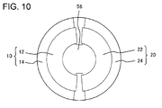
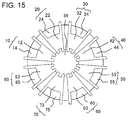
- An example of one-and-one is shown in Fig. 10, Fig. 11 and Fig. 12, and an example of four-and-four is shown in Fig. 13, Fig. 14 and Fig. 15.
- Fig. 10 In Fig. 10, Fig. 11 and Fig. 12, two FETs composed of the FET 10 and the FET 20 are provided.
- the FET 10 and the FET 20 constitute a FET pair.
- Fig. 11 illustrates an example of the end portion of the gate electrode being protruded toward the outside of the circle, similarly as in Fig. 8.
- Fig. 12 illustrates an example of the end portion of the gate electrode being protruded toward both of the outside and the inside of a circle, similarly as in Fig. 9.
- FETs 10, 20, 30, 40, 50, 60, 70 and 80 are provided.
- the FETs 50, 60, 70 and 80 have gate electrodes 53, 63, 73 and 83, respectively. Further, the FETs 50, 60, 70 and 80 have diffusion layers 55, 65, 75 and 85 functioning as drain regions, respectively.
- electrical couplings are formed among the source region, the gate electrode and the drain region.
- electrical couplings are formed among the source region, the gate electrode and the drain region.
- an FET pair is constituted by an FET composed of the FETs 10, 30, 50 and 70 and an FET composed of the FETs 20, 40, 60 and 80.
- Fig. 14 illustrates an example of the end portion of the gate electrode being protruded toward the outside of the circle, similarly as in Fig. 8.
- Fig. 15 illustrates an example of the end portion of the gate electrode being protruded toward both of the outside and the inside of a circle, similarly as in Fig. 9.
- each of the FETs 10, 20, 30 and 40 may alternatively functions as an independent FET.
- two FET pairs composed of the FET pair constituted by the FETs 10 and 20 and the FET pair constituted by the FETs 30 and 40 can be formed in an active region.
- the gate electrodes 12, 22, 32 and 42 being arranged along a circumference of a complete circle have been illustrated.
- the gate electrodes 12, 22, 32 and 42 may alternatively be arranged along a circumference of a polygon that is similar to a circle, instead of the circumference of the complete circle. Even in such case, it can also be considered that the gate electrodes 12, 22, 32 and 42 are arranged along a circle.
- diffusion layer 56 in the inside of the gate electrode functioning as a source region
- diffusion layer may function as a drain region
- a diffusion layer outside of the gate electrode may function as a source region.
- the present invention may also be preferably applied to an operational amplifier.
Landscapes
- Metal-Oxide And Bipolar Metal-Oxide Semiconductor Integrated Circuits (AREA)
- Semiconductor Integrated Circuits (AREA)
Abstract
Description
- This application is based on
Japanese patent application No. 2006-154313 - The present invention relates to a semiconductor device.
- In relation to semiconductor devices having a plurality of field effect transistors (FETs), higher pair accuracy or namely higher relativity accuracy is often required between those FETs. For example, in relation to an operational amplifier or a differential circuit in comparator, or a pair FETs constituting a mirror circuit, high pair accuracy is required for reducing an input off-set voltage for such operational amplifier or such comparator.
- Typical conventional semiconductor devices provided with a plurality of FETs include semiconductor devices described in
Japanese Patent Laid-Open No. S62-81054 No. 1987-81054 Japanese Patent Laid-Open No. H06-13574 No. 1994-13574 - Fig. 16 is a plan view, showing a semiconductor device described in
Japanese Patent Laid-Open No. S62-81054 semiconductor device 100 includes fourFETs annular gate electrode 111, and asource electrode 112 and adrain region 113 provided in the outside and the inside thereof, respectively. In theFET 101 and theFET 103, the source electrode, the gate electrode and the drain electrode are electrically coupled with each other. A coupling situation between the FET 102 and the FET 104 is similar to that between the FET 101 and the FET 103. - Therefore, in the
semiconductor device 100, a combination of the FET 101 and the FET 103 substantially functions as one FET and a combination of the FET 102 and the FET 104 substantially functions as another FET. Then, the FET composed of the FETs 101 and 103 and the FET composed of theFETs - Fig. 17 is a plan view, showing a semiconductor device described in
Japanese Patent Laid-Open No. H06-13574 semiconductor device 200, an FET 210a and an FET 210b constituting an FET pair are also provided. The FETs 210a and 210b share asource region 201. The FET 210a has agate electrode 202a and adrain region 203a. Similarly, the FET 210b has agate electrode 202b and adrain region 203b. - In addition to above, another prior art document related to the present invention is Japanese Patent Laid-Open
No. H02-210864 (1990 Japanese Patent Laid-Open No. S62-81054 Japanese Patent Laid-Open No. H06-13574 - In the
semiconductor device 100 of Fig. 16, the FETs 101,102,103 and 104 are disposed to be spaced apart from each other. In such configuration, the pair accuracies of the FET-pairs composed of such FETs are more easily affected by a variation of impurity concentration in the diffusion layer in the substrate surface, as compared with the configuration, in which these are disposed closely with each other. - Besides, in the
semiconductor device 200 of Fig. 17, geometries of therespective gate electrodes gate electrode - As described above, in relation to the conventional semiconductor device provided with a plurality of FETs, there is room for improving the pair accuracy of the FET-pair.
- According to one aspect of the present invention, there is provided a semiconductor device comprising: a plurality of field effect transistors provided in a certain region defined by an element isolation region, wherein gate electrodes of the plurality of field effect transistors are arranged along a circle in plan view, and wherein at least two field effect transistors selected from the plurality of field effect transistors have substantially same geometry.
- In such semiconductor device, a plurality of FETs are provided in a certain region. Thus, these FETs are more easily arranged to be closer to each other, as compared with a case of providing the FETs in different certain regions, respectively. Therefore, the pair accuracy of the FET-pair composed of these FETs is difficult to be influenced by a variation of an impurity concentration in the diffusion layer in the substrate surface. Further, the gate electrodes of the FETs are arranged along a circle. Thus, unlikely with the semiconductor device shown in Fig. 17, a deviation in an electric current flowing through the source and the drain can be prevented.
- According to the present invention, a semiconductor device having a constitution that is suitable in improving a pair accuracy of an FET-pair is achieved.
- The above and other objects, advantages and features of the present invention will be more apparent from the following description of certain preferred embodiments taken in conjunction with the accompanying drawings, in which:
- Fig. 1 is a plan view, illustrating first embodiment of a semiconductor device according to the present invention;
- Fig. 2 is a plan view, useful in describing a two-dimensional geometry of a gate electrode in the semiconductor device of Fig. 1;
- Figs. 3A and 3B are cross-sectional views, illustrating a cross section along line III-III of the semiconductor device shown in Fig. 1;
- Fig. 4A and 4B are cross-sectional view, illustrating cross section along line IV-IV of the semiconductor device shown in Fig. 1;
- Fig. 5 is a circuit architecture diagram, illustrating a configuration of a general comparator;
- Fig. 6 is also a circuit architecture diagram, illustrating a configuration of a general comparator;
- Fig. 7 a plan view, illustrating an example of a circuit layout, in which the present invention is applied to the comparator shown in Fig. 5;
- Fig. 8 is a plan view, illustrating second embodiment of a semiconductor device according to the present invention;
- Fig. 9 is a plan view, illustrating third embodiment of a semiconductor device according to the present invention;
- Fig. 10 is a plan view, illustrating a modified example in the preferred embodiments;
- Fig. 11 is a plan view, illustrating another modified example in the preferred embodiments;
- Fig. 12 is a plan view, illustrating further modified example in the preferred embodiments;
- Fig. 13 is a plan view, illustrating yet other modified example in the preferred embodiments;
- Fig. 14 is a plan view, illustrating yet other modified example in the preferred embodiments;
- Fig. 15 is a plan view, illustrating yet other modified example in the preferred embodiments;
- Fig. 16 is a plan view, illustrating a semiconductor device described in
Japanese Patent Laid-Open No. S62-81054 - Fig. 17 is a plan view, illustrating a semiconductor device described in Japanese Patent Laid-Open No. H06-13574; and
- Fig. 18 is a plan view, illustrating another semiconductor devices described in Japanese Patent Laid-Open
No. S62-81054 - The invention will be now described herein with reference to illustrative embodiments. Those skilled in the art will recognize that many alternative embodiments can be accomplished using the teachings of the present invention and that the invention is not limited to the embodiments illustrated for explanatory purposed.
- Exemplary implementations of semiconductor devices according to the present invention will be described in reference to the annexed figures. In all figures, identical numeral is assigned to an element commonly appeared in the description of the present invention in reference to the figures, and the detailed description thereof will not be repeated.
- Fig. 1 is a plan view, showing first embodiment of a semiconductor device according to the present invention. A
semiconductor device 1 includes an FET 10 (first FET), an FET 20 (second FET), an FET 30 (third FET) and an FET 40 (fourth FET). TheseFETs - The
FET 10, theFET 20, theFET 30 and theFET 40 have agate electrode 12, agate electrode 22, agate electrode 32 and agate electrode 42, respectively. Thegate electrode 12, thegate electrode 22, thegate electrode 32 and thegate electrode 42 are arranged along a circle in this sequence in plan view. Materials of thegate electrodes - Besides, the
FETs gate electrodes gate electrodes gate electrode 12. - Returning to Fig. 1, the outside of the above-described circle in plan view, or in other words, the outside of the
gate electrode diffusion layers diffusion layer 14 with thegate electrode 12 and thediffusion layer 56 as discuss later, constitute theFET 10. Thediffusion layer 24 with thegate electrode 22 and thediffusion layer 56, constitute theFET 20. Thediffusion layer 34 with thegate electrode 32 and thediffusion layer 56, constitute theFET 30. Further, thediffusion layer 44 with thegate electrode 42 and thediffusion layer 56, constitute theFET 40. The diffusion layers 14, 24, 34 and 44 function as drain regions of theFETs - The inside of the above-described circle in plan view is, or in other words, the insides of the
gate electrodes diffusion layer 56 is shared by theFETs diffusion layer 56 functions as source regions of theFETs - In the configuration according to the present embodiment, the source region (diffusion layer 56), the
gate electrode 32 and the drain region (diffusion layer 34) of theFET 30 are electrically coupled to the source region (diffusion layer 56), thegate electrode 12 and the drain region (diffusion layer 14) of theFET 10, respectively. Similarly, the source region (diffusion layer 56), thegate electrode 42 and the drain region (diffusion layer 44) of theFET 40 are electrically coupled to the source region (diffusion layer 56), thegate electrode 22 and the drain region (diffusion layer 24) of theFET 20, respectively. - Therefore, in the
semiconductor device 1, one combination of theFET 10 and theFET 30 substantially function as an FET, and another combination of theFET 20 and theFET 40 substantially function as another FET. Thus, an FET pair is constituted of the FET, which is composed of theFETs FET - Fig. 3A and Fig. 3B are cross-sectional views, showing cross sections along line III-III of the
semiconductor device 1 of Fig. 1. Fig. 4A and Fig. 4B are cross-sectional views, showing cross sections along line IV-IV of thesemiconductor device 1 of Fig. 1. In these cross-sections, Fig. 3A and Fig. 4A represent N-channel FETs channel FETs - As can be seen from these cross-sectional views, the above-described
gate electrodes semiconductor substrate 61. On the other hand, the diffusion layers 14, 24, 34 and 44 and thediffusion layer 56 are formed in thesemiconductor substrate 61. The diffusion layers 14, 24, 34 and 44 and thediffusion layer 56 are N+ type when theFETs FETs - The
semiconductor substrate 61 includes an N-type substrate 62 and an N-type epitaxial layer 64 formed thereon. However, it is not essential to provide theepitaxial layer 64 in thesemiconductor substrate 61. When theFET type well region 66 is further formed in a surface layer of thesemiconductor substrate 61. Further, thesemiconductor substrate 61 is provided with anelement isolation region 68 formed therein. Typical configuration of theelement isolation region 68 includes shallow trench isolation (STI) or local oxidation of silicon (LOCOS). - An interlayer insulating
film 72 is also provided on thesemiconductor substrate 61. Further, thesource electrode 57 is coupled to thediffusion layer 56 via an opening formed in theinterlayer insulating film 72, and, thedrain electrode 15 and thedrain electrode 35 are coupled to thediffusion layer 14 and thediffusion layer 34, respectively. In addition to above, the diffusion layers 24 and 44, which do not appear in the cross-sectional view of Fig. 4A or Fig. 4B, are coupled to the drain electrodes, similarly as thediffusion layer interlayer insulating film 72, thesource electrode 57 and thedrain electrode - Suitable applications of the present invention will be described in reference to Fig. 5 and Fig. 6. Fig. 5 and Fig. 6 are circuit architecture diagrams, showing a general comparator. A comparator presented in these diagrams includes a
differential circuit 82 and amirror circuit 84. Thedifferential circuit 82 is constituted of an FET pair, which is composed of two N-channel FETs (MN1 and MN2) in the exemplary implementation shown in Fig. 5, and is alternatively constituted of an FET pair, which is composed of two P-channel FETs (MP3 and MP4) in the exemplary implementation shown in Fig. 6. Besides, themirror circuit 84 is constituted of an FET pair, which is composed of two P-channel FETs (MP1 and MP2) in the exemplary implementation shown in Fig. 5, and is alternatively constituted of an FET pair, which is composed of two N-channel FETs (MN3 and MN4) in the exemplary implementation shown in Fig. 6. In Fig. 5, sources of FETs (MP1, MP2, MN1 and MN2) are represented by SP1, SP2, SN1 and SN2, gates of FETs (MP1, MP2, MN1 and MN2) are represented by GP1, GP2, GN1 and GN2, and drains of FETs (MP1, MP2, MN1 and MN2) are represented by DP1, DP2, DN1 and DN2, respectively. In Fig. 6, sources of FETs (MP3, MP4, MN3 and MN4) are represented by SP3, SP4, SN3 and SN4, gates of FETs (MP3, MP4, MN3 and MN4) are represented by GP3, GP4, GN3 and GN4, and drains of FETs (MP3, MP4, MN3 and MN4) are represented by DP3, DP4, DN3 and DN4, respectively. - The present invention may be preferably applied to the comparator having such configuration. For example, taking the
differential circuit 82 as an example, the FET composed of theFETs FETs mirror circuit 84, and specifically, the FET composed of theFETs FETs - Fig. 7 is a plan view, showing an example of a circuit layout in a case of applying the present invention to the comparator of Fig. 5. In this exemplary implementation, a differential circuit (
differential circuit 82 of Fig. 5) is disposed in an active region R1 in an upper section of the diagram, and a mirror circuit (mirror circuit 84 of Fig. 5) is disposed in an active region R1 in a lower section of the diagram. Concerning the differential circuit, theFETs FETs FETs FETs metallic interconnect 94. Here, a numeral 92 in Fig. 7 represents a polysilicon. - Advantageous effects obtainable by employing the configuration of the present embodiment will be described. In Fig. 5, an improved pair accuracy of the FET pair (NM1 and MN2) of the
differential circuit 82 allows a reduced input off-set voltage of the comparator. Further, an improved pair accuracy of the FET pair (NP1 and MP2) of themirror circuit 84 allows a reduced input off-set voltage of the comparator. In thesemiconductor device 1, as described in reference to Fig. 7, theFETs - Further, the
gate electrodes respective FETs semiconductor device 1 having the structure suitable in improving the pair accuracy of the FET pair can be achieved. - Since the
FETs semiconductor device 1. On the contrary, when a plurality of FETs are provided in separate active regions as shown by the semiconductor device in Fig. 16, an area occupied by these FETs is increased. - In reference to Fig. 7, for example, the pair accuracy of the FET pair can be provided if the
FETs FETs FETs FETs FETs FETs - Fig. 18 is a plan view, showing a conventional semiconductor device comprising a plurality of FETs having different geometries. The
semiconductor device 300 is described inJapanese Patent Laid-Open No. S62-81054 gate electrode 311a and agate electrode 311b are provided in thesemiconductor device 300. Thegate electrodes gate electrode 311a with thesource electrode 312a, constitute an FET. Further, thegate electrode 311b,with_the source electrode 312b, constitute another FET. These two FETs share adrain electrode 313. Since thesemiconductor device 300 is easily affected by a dimension difference, resulting in a deteriorated dimensional accuracy, it is difficult to control an area ratio of the channel-forming regions of two FETs with higher accuracy. - In the
semiconductor device 1, as described in reference to Fig. 2, the geometries of therespective gate electrodes - It is configured that a combination of the
FET 10 and theFET 30 substantially function as an FET, and another combination of theFET 20 and theFET 40 substantially function as another FET. This allows that the pair accuracy of the FET pair composed of these FETs is further difficult to be influenced by a variation of an impurity concentration in the diffusion layer in the substrate surface. For example, when a single-dimensional concentration gradient is present, in which an impurity concentration is lower as closer to the right end in the diagram of Fig. 1, the diffusion layers of theFET 10 and theFET 40 have relatively higher concentrations, and the diffusion layers of theFET 20 and theFET 30 have relatively lower concentrations. Therefore, the above described configuration results in that both of the FET composed of theFETs FETs - The
diffusion layer 56 is shared by theFETs semiconductor device 1 to circuits such as a differential circuit or a mirror circuit, employing the FET pair having source regions that are mutually coupled. In particular, as illustrated in Fig. 5 and Fig. 6, if the semiconductor device is applied to a differential circuit or a mirror circuit of a comparator, an input off-set voltage of the comparator can be reduced. - Fig. 8 is a plan view, showing second embodiment of a semiconductor device according to the present invention. In a
semiconductor device 2, the configurations of thegate electrodes semiconductor device 1 described in reference to Fig. 1. Other configurations of thesemiconductor device 2 are similar to that of thesemiconductor device 1. - In the
semiconductor device 2, anend portion 12a of agate electrode 12 protrudes toward the outside of the above-described circle. The protruded section defines an end portion of adiffusion layer 14. Such protruded section extends to the outside of an active region R1. This provides thediffusion layer 14 being completely surrounded by thegate electrode 12 and an element isolation region, in plan view. The configurations of thegate electrodes gate electrode 12. - Here, concerning dependencies for a dimensional accuracy of a channel-forming region, the
semiconductor device 2 is compared with thesemiconductor device 1. For simplicity, the exemplary implementation will be made in reference to theFET 10. In thesemiconductor device 1, a dimensional accuracy of the channel-forming region depends upon three parameters, namely: a dimensional accuracy in the geometry of the gate electrode 12 (polysilicon, for example); a dimensional accuracy in the geometry of thediffusion layer 14; and a dimensional accuracy in the geometry of thediffusion layer 56. On the other hand, in thesemiconductor device 2, a dimensional accuracy of the channel-forming region depends upon two parameters, namely: a dimensional accuracy in the geometry of thegate electrode 12; and a dimensional accuracy in the geometry of thediffusion layer 56. Therefore, according to thesemiconductor device 2, more improved pair accuracy of the FET pair can be achieved, as compared with thesemiconductor device 1. Other advantageous effects of thesemiconductor device 2 are similar to that of thesemiconductor device 1. - Fig. 9 is a plan view, showing third embodiment of a semiconductor device according to the present invention. In a
semiconductor device 3, the configurations of thegate electrodes semiconductor device 1 described in reference to Fig. 1. Other configurations of thesemiconductor device 3 are similar to that of thesemiconductor device 1. - In the
semiconductor device 3, anend portion 12a of agate electrode 12 protrudes toward both of the outside and the inside of the above-described circle. It is similar as described for thesemiconductor device 2 in reference to Fig. 8 that the protruded section defines an end portion of adiffusion layer 14. Insemiconductor device 3, the additional inwardly-protruded section defines an end portion of a section adjacent thegate electrode 12 in thediffusion layer 56. The configurations of thegate electrodes gate electrode 12. - In the
semiconductor device 3 having such configuration, a dimensional accuracy of the channel-forming region depends only a dimensional accuracy in the geometry of thegate electrode 12. Therefore, thesemiconductor device 3 can provide more improved pair accuracy of the FET pair can be achieved, as compared with thesemiconductor device 2. Other advantageous effects of thesemiconductor device 3 are similar to that of thesemiconductor device 2. In addition to above, in all of thesemiconductor devices gate electrodes - In the present embodiment, the
end portion 12a may be protruded only toward the inside of the above-described circle. In such case, a dimensional accuracy of the channel-forming region depends upon two parameters, namely: a dimensional accuracy in the geometry of the ateelectrode 12; and a dimensional accuracy in the geometry of thediffusion layer 14. Therefore, such semiconductor device can provide more improved pair accuracy of the FET pair can be achieved, as compared with thesemiconductor device 1. - It is not intended that the semiconductor device according to the present invention is limited to the configurations illustrated in the above-described embodiments, and thus various modifications thereof are also available. For example, in the above-described embodiments, exemplary implementations of the four FETs constituting FET pairs, which are divided by 2 FETs to 2 FETs, have been illustrated. More specifically, exemplary implementations of the FET pairs, which are constituted by the FET composed of two
FETs FETs - In Fig. 10, Fig. 11 and Fig. 12, two FETs composed of the
FET 10 and theFET 20 are provided. TheFET 10 and theFET 20 constitute a FET pair. In these diagrams, Fig. 11 illustrates an example of the end portion of the gate electrode being protruded toward the outside of the circle, similarly as in Fig. 8. Further, Fig. 12 illustrates an example of the end portion of the gate electrode being protruded toward both of the outside and the inside of a circle, similarly as in Fig. 9. - In Fig. 13, Fig. 14 and Fig. 15, eight
FETs FETs gate electrodes FETs diffusion layers FETs FETs FETs FETs - Further, in the above-described embodiments, in the above-described embodiment, exemplary implementations of two FETs among the
FETs FETs FETs FETs - In the above-described embodiments, exemplary implementations of the
gate electrodes gate electrodes gate electrodes - In the above-described embodiments, exemplary implementations of all FETs in the active region R1 having the same geometry, have been illustrated. Alternatively, if three or more FETs are provided in the active region R1, it is sufficient that at least two FETs have the same geometry.
- In the above-described embodiments, exemplary implementations of the diffusion layer (diffusion layer 56) in the inside of the gate electrode functioning as a source region have been illustrated. Alternatively, such diffusion layer may function as a drain region, and a diffusion layer outside of the gate electrode may function as a source region.
- In the above-described embodiments, exemplary implementations of applying the present invention to a comparator have been illustrated. Alternatively, the present invention may also be preferably applied to an operational amplifier.
- It is apparent that the present invention is not limited to the above embodiment, and may be modified and changed without departing from the scope and spirit of the invention.
Claims (12)
- A semiconductor device, comprising:a plurality of field effect transistors (FETs) provided in a certain region defined by an element isolation region,wherein gate electrodes of said plurality of field effect transistors are arranged along a circle in plan view, andwherein at least two field effect transistors selected from said plurality of field effect transistors have substantially same geometry.
- The semiconductor device as set forth in claim 1, wherein each of said gate electrodes has a geometry that is substantially equivalent to a partial annular circle, which is prepared by eliminating a second sector from a first sector in plan view, said first sector having a center, which is equivalent to a center of said circle, and said second sector having a center, which is also equivalent to the center of said circle, and having a radius, which is shorter than a radius of said first sector.
- The semiconductor device as set forth in claim 1 or 2, wherein said plurality of field effect transistors include a first, a second, a third and a fourth field effect transistors, and
said gate electrodes of said first, said second, said third and said fourth field effect transistors are arranged in this sequence along said circle. - The semiconductor device as set forth in claim 3, wherein a source region, a gate electrode and a drain region of said third field effect transistor are electrically coupled to a source region, a gate electrode and a drain region of said first field effect transistor, respectively, and wherein a source region, a gate electrode and a drain region of said fourth field effect transistor are electrically coupled to a source region, a gate electrode and a drain region of said second field effect transistor, respectively.
- The semiconductor device as set forth in any of claims 1 to 4, further comprising a first and a second diffusion layers provided in the outside and the inside of said circle in plan view, respectively, wherein one of said first and said second diffusion layers functions as a source region of said field effect transistor, and the other functions as a drain region of said field effect transistor.
- The semiconductor device as set forth in claim 5, wherein
an end portion of said gate electrode protrudes toward the outside of said circle, and wherein an end of said first diffusion layer is defined by the protruded section. - The semiconductor device as set forth in claim 6, wherein an end portion of said gate electrode protrudes toward the inside of said circle, and wherein an end of a portion of said second diffusion layer adjacent said gate electrode is defined by the protruded section.
- The semiconductor device as set forth in any of claims 5 to 7, wherein said plurality of field effect transistors share said second diffusion layer.
- The semiconductor device as set forth in claim 8, wherein said second diffusion layer functions as a source region of each of said field effect transistors.
- The semiconductor device as set forth in any of claims 1 to 9, wherein said plurality of field effect transistors include a pair of field effect transistors, each of which has a source region, said source regions of said pair of field effect transistors being mutually electrically coupled.
- The semiconductor device as set forth in claim 10, wherein said pair of field effect transistors constitute one of a differential circuit and a mirror circuit.
- The semiconductor device as set forth in claim 10, wherein said pair of field effect transistors constitute one of a differential circuit and a mirror circuit in one of an operational amplifier and a comparator.
Applications Claiming Priority (1)
| Application Number | Priority Date | Filing Date | Title |
|---|---|---|---|
| JP2006154313A JP2007324438A (en) | 2006-06-02 | 2006-06-02 | Semiconductor device |
Publications (2)
| Publication Number | Publication Date |
|---|---|
| EP1863088A2 true EP1863088A2 (en) | 2007-12-05 |
| EP1863088A3 EP1863088A3 (en) | 2010-11-24 |
Family
ID=38328533
Family Applications (1)
| Application Number | Title | Priority Date | Filing Date |
|---|---|---|---|
| EP07010724A Withdrawn EP1863088A3 (en) | 2006-06-02 | 2007-05-30 | FET semiconductor device with partial annular gate electrodes |
Country Status (3)
| Country | Link |
|---|---|
| US (1) | US7675089B2 (en) |
| EP (1) | EP1863088A3 (en) |
| JP (1) | JP2007324438A (en) |
Cited By (1)
| Publication number | Priority date | Publication date | Assignee | Title |
|---|---|---|---|---|
| CN103636002A (en) * | 2011-05-19 | 2014-03-12 | 惠普发展公司,有限责任合伙企业 | Device active channel aspect ratio greater than the channel aspect ratio |
Family Cites Families (8)
| Publication number | Priority date | Publication date | Assignee | Title |
|---|---|---|---|---|
| US4546453A (en) * | 1982-06-22 | 1985-10-08 | Motorola, Inc. | Four-state ROM cell with increased differential between states |
| JPS6281054A (en) | 1985-10-04 | 1987-04-14 | Nec Corp | Semiconductor device |
| JPH02210864A (en) | 1989-02-09 | 1990-08-22 | Matsushita Electron Corp | Semiconductor integrated circuit device |
| EP0466463A1 (en) * | 1990-07-10 | 1992-01-15 | Kawasaki Steel Corporation | Basic cell and arrangement structure thereof |
| JP2713082B2 (en) | 1992-03-27 | 1998-02-16 | 松下電器産業株式会社 | Semiconductor device |
| TW377493B (en) * | 1996-12-27 | 1999-12-21 | Matsushita Electric Industrial Co Ltd | Semiconductor integrated circuit device |
| US7005713B2 (en) * | 2003-12-01 | 2006-02-28 | The Aerospace Corporation | Annular segmented MOSFET |
| US7294892B2 (en) * | 2005-05-27 | 2007-11-13 | Faraday Technology Corp. | Multi-transistor layout capable of saving area |
-
2006
- 2006-06-02 JP JP2006154313A patent/JP2007324438A/en not_active Withdrawn
-
2007
- 2007-05-30 EP EP07010724A patent/EP1863088A3/en not_active Withdrawn
- 2007-05-30 US US11/806,232 patent/US7675089B2/en not_active Expired - Fee Related
Cited By (5)
| Publication number | Priority date | Publication date | Assignee | Title |
|---|---|---|---|---|
| CN103636002A (en) * | 2011-05-19 | 2014-03-12 | 惠普发展公司,有限责任合伙企业 | Device active channel aspect ratio greater than the channel aspect ratio |
| EP2710637A4 (en) * | 2011-05-19 | 2014-08-06 | Hewlett Packard Development Co | LENGTH / ACTIVE CHANNEL WIDTH OF DEVICE GREATER THAN LENGTH / CHANNEL WIDTH |
| CN103636002B (en) * | 2011-05-19 | 2016-10-26 | 惠普发展公司,有限责任合伙企业 | Device active channel aspect ratio greater than the channel aspect ratio |
| US9773782B2 (en) | 2011-05-19 | 2017-09-26 | Hewlett-Packard Development Company, L.P. | Transistor having an active channel region |
| US10170466B2 (en) | 2011-05-19 | 2019-01-01 | Hewlett-Packard Development Company, L.P. | Device having an active channel region |
Also Published As
| Publication number | Publication date |
|---|---|
| US7675089B2 (en) | 2010-03-09 |
| JP2007324438A (en) | 2007-12-13 |
| US20070278522A1 (en) | 2007-12-06 |
| EP1863088A3 (en) | 2010-11-24 |
Similar Documents
| Publication | Publication Date | Title |
|---|---|---|
| JPH0997885A (en) | Gate array | |
| US10825814B2 (en) | Semiconductor device | |
| CN1866541B (en) | Field effect transistor and method for manufacturing same | |
| CN104979349B (en) | Semiconductor device | |
| JP2018195775A (en) | Semiconductor device | |
| US20010019166A1 (en) | Semiconductor devices | |
| US10431655B2 (en) | Transistor structure | |
| US8110454B2 (en) | Methods of forming drain extended transistors | |
| JP3457539B2 (en) | Semiconductor device | |
| TWI392083B (en) | Semiconductor device | |
| US20050230751A1 (en) | Semiconductor device | |
| US10373862B2 (en) | Semiconductor device | |
| JP4864344B2 (en) | Semiconductor device | |
| JP2676888B2 (en) | Semiconductor device | |
| US7675089B2 (en) | Semiconductor device | |
| JP2015095492A (en) | Semiconductor device | |
| US6320233B1 (en) | CMOS semiconductor device | |
| EP0373631B1 (en) | MOS transistor and differential amplifier circuit with low offset | |
| US7211870B2 (en) | Semiconductor device | |
| JP2007019413A (en) | Semiconductor device for protection circuit | |
| US6492687B2 (en) | Merged semiconductor device and method | |
| US11587869B2 (en) | Semiconductor device and method of manufacturing the same | |
| JP6674056B2 (en) | Semiconductor device | |
| US11121264B2 (en) | Junction field effect transistor | |
| JPH10294383A (en) | Input protection diode |
Legal Events
| Date | Code | Title | Description |
|---|---|---|---|
| PUAI | Public reference made under article 153(3) epc to a published international application that has entered the european phase |
Free format text: ORIGINAL CODE: 0009012 |
|
| AK | Designated contracting states |
Kind code of ref document: A2 Designated state(s): AT BE BG CH CY CZ DE DK EE ES FI FR GB GR HU IE IS IT LI LT LU LV MC MT NL PL PT RO SE SI SK TR |
|
| AX | Request for extension of the european patent |
Extension state: AL BA HR MK YU |
|
| RAP1 | Party data changed (applicant data changed or rights of an application transferred) |
Owner name: RENESAS ELECTRONICS CORPORATION |
|
| PUAL | Search report despatched |
Free format text: ORIGINAL CODE: 0009013 |
|
| AK | Designated contracting states |
Kind code of ref document: A3 Designated state(s): AT BE BG CH CY CZ DE DK EE ES FI FR GB GR HU IE IS IT LI LT LU LV MC MT NL PL PT RO SE SI SK TR |
|
| AX | Request for extension of the european patent |
Extension state: AL BA HR MK RS |
|
| REG | Reference to a national code |
Ref country code: DE Ref legal event code: R108 |
|
| AKY | No designation fees paid | ||
| REG | Reference to a national code |
Ref country code: DE Ref legal event code: R108 Effective date: 20110720 |
|
| STAA | Information on the status of an ep patent application or granted ep patent |
Free format text: STATUS: THE APPLICATION IS DEEMED TO BE WITHDRAWN |
|
| 18D | Application deemed to be withdrawn |
Effective date: 20110525 |