EP1863023A2 - Optical disc apparatus and recording power control method - Google Patents
Optical disc apparatus and recording power control method Download PDFInfo
- Publication number
- EP1863023A2 EP1863023A2 EP07109206A EP07109206A EP1863023A2 EP 1863023 A2 EP1863023 A2 EP 1863023A2 EP 07109206 A EP07109206 A EP 07109206A EP 07109206 A EP07109206 A EP 07109206A EP 1863023 A2 EP1863023 A2 EP 1863023A2
- Authority
- EP
- European Patent Office
- Prior art keywords
- power
- current
- erase
- emission
- laser light
- Prior art date
- Legal status (The legal status is an assumption and is not a legal conclusion. Google has not performed a legal analysis and makes no representation as to the accuracy of the status listed.)
- Withdrawn
Links
- 230000003287 optical effect Effects 0.000 title claims description 40
- 238000000034 method Methods 0.000 title claims description 30
- 238000010586 diagram Methods 0.000 description 10
- 238000005070 sampling Methods 0.000 description 7
- 230000004044 response Effects 0.000 description 6
- 238000001514 detection method Methods 0.000 description 5
- 101100371162 Mus musculus Tslp gene Proteins 0.000 description 3
- 101100049053 Mus musculus Vash1 gene Proteins 0.000 description 3
- 238000007796 conventional method Methods 0.000 description 2
- 230000003247 decreasing effect Effects 0.000 description 2
- 230000000630 rising effect Effects 0.000 description 2
- 230000015556 catabolic process Effects 0.000 description 1
- 238000012937 correction Methods 0.000 description 1
- 238000006731 degradation reaction Methods 0.000 description 1
- 238000009499 grossing Methods 0.000 description 1
- 238000004519 manufacturing process Methods 0.000 description 1
- 238000005259 measurement Methods 0.000 description 1
- 230000002123 temporal effect Effects 0.000 description 1
- 238000012360 testing method Methods 0.000 description 1
Images



Classifications
-
- G—PHYSICS
- G11—INFORMATION STORAGE
- G11B—INFORMATION STORAGE BASED ON RELATIVE MOVEMENT BETWEEN RECORD CARRIER AND TRANSDUCER
- G11B7/00—Recording or reproducing by optical means, e.g. recording using a thermal beam of optical radiation by modifying optical properties or the physical structure, reproducing using an optical beam at lower power by sensing optical properties; Record carriers therefor
- G11B7/12—Heads, e.g. forming of the optical beam spot or modulation of the optical beam
- G11B7/125—Optical beam sources therefor, e.g. laser control circuitry specially adapted for optical storage devices; Modulators, e.g. means for controlling the size or intensity of optical spots or optical traces
- G11B7/126—Circuits, methods or arrangements for laser control or stabilisation
- G11B7/1263—Power control during transducing, e.g. by monitoring
-
- G—PHYSICS
- G11—INFORMATION STORAGE
- G11B—INFORMATION STORAGE BASED ON RELATIVE MOVEMENT BETWEEN RECORD CARRIER AND TRANSDUCER
- G11B7/00—Recording or reproducing by optical means, e.g. recording using a thermal beam of optical radiation by modifying optical properties or the physical structure, reproducing using an optical beam at lower power by sensing optical properties; Record carriers therefor
- G11B7/004—Recording, reproducing or erasing methods; Read, write or erase circuits therefor
- G11B7/0045—Recording
-
- G—PHYSICS
- G11—INFORMATION STORAGE
- G11B—INFORMATION STORAGE BASED ON RELATIVE MOVEMENT BETWEEN RECORD CARRIER AND TRANSDUCER
- G11B7/00—Recording or reproducing by optical means, e.g. recording using a thermal beam of optical radiation by modifying optical properties or the physical structure, reproducing using an optical beam at lower power by sensing optical properties; Record carriers therefor
- G11B7/004—Recording, reproducing or erasing methods; Read, write or erase circuits therefor
- G11B7/0045—Recording
- G11B7/00456—Recording strategies, e.g. pulse sequences
Definitions
- This invention relates to the technique for recording information onto a recordable optical disc, such as CD-R, CD-RW, DVD-R, DVD-RW, DVD-RAM, HDDVD-R, HDDVD-RAM, or HDDVD-RW, and more particularly to control of recording power.
- a recordable optical disc such as CD-R, CD-RW, DVD-R, DVD-RW, DVD-RAM, HDDVD-R, HDDVD-RAM, or HDDVD-RW
- a rewritable optical disc For example, in a rewritable optical disc, groove and/or land tracks are formed on the disc surface, recording layers are formed at the tracks, and a beam spot of laser light is caused to follow a track, thereby forming or erasing recording marks.
- the driving-current-to-emission-power characteristic of a laser diode used for an optical disc fluctuates according to temperature change or temporal change. To improve the recording performance, it is important to control the emission power so that the power may be constant.
- a conventional power control method first, the value of recording power (peak power) in the mark part, the value of recording power (erase power) in the space part, and the value of bottom power in a multi-pulse are held. Then, on the basis of the held values and the ratio of the erase power to preset peak power and bottom power, erase power is calculated.
- the recording pulse is controlled so that the actual intensity levels of the peak power, bottom power, and erase power may coincide with respective target values (Jpn. Pat. Appln. KOKAI Publication No. 2000-30276 ).
- APC Auto Power Control
- an object of the invention to provide control whereby an LD is caused to always emit light with required power without using a high-priced fast response/high accuracy peak hold circuit or broadband monitor, even if a fluctuation in the characteristic of the LD occurs due to temperature changes.
- the I-L characteristic the current-to-emission-power characteristic of an LD using the average power and erase power in recording that can be measured with a narrowband peak hold circuit without using a broadband peak hold circuit and determining a current setting value to obtain an arbitrary power level.
- the I-L characteristic fluctuates due to temperature changes or time degradation, it is necessary to determine a driving current value that causes the optimum power to be generated constantly. At this time, if the latest I-L characteristic is known, not only can a constant emission level be kept, but also a current value to obtain a new target level can be known immediately, even when the target level is changed in learning or testing the write characteristic. Therefore, it is possible to control the emission power level instantaneously without going through transitional conditions in feedback control of conventional emission power.
- an LD is caused to always emit light with required power without using a high-priced fast response/high accuracy peak hold circuit or broadband monitor, even if the characteristic of the LD fluctuates due to temperature changes.
- FIG. 1 is a block diagram showing an example of the configuration of an optical disc apparatus to which the invention is applied.
- the optical disc apparatus records and reproduces information onto and from an information storage medium, or an optical disc 100, such as a DVD (Digital Versatile Disc).
- an optical disc 100 such as a DVD (Digital Versatile Disc).
- grooves are cut concentrically or spirally.
- the concave parts are called lands and the convex parts are called grooves.
- One round of a groove or a land is called a track.
- Intensity-modulated laser light is applied along the track (or only a groove or both a groove and a land) to form recording marks, thereby recording user data.
- the data is reproduced by applying read-power laser light weaker than in recording to the track and detecting changes in the reflected light intensity caused by recording marks on the track.
- the recorded data is erased by applying erase-power laser light higher than the read power to the track to crystallize the recording layer.
- the optical disc 100 is rotated by a spindle motor 63.
- a rotation detector 63a provided on the spindle motor 63 supplies FG pulses. When the spindle motor 63 makes one revolution, for example, five FG pulses are generated. From the FG pulses, the rotation angle and rotation number of the spindle motor 63 can be determined.
- optical pickup 65 Information is recorded onto and reproduced from the optical disc 100 by an optical pickup 65.
- the optical pickup 65 is coupled with a sled motor 66 via a gear.
- the sled motor 66 is controlled by a sled motor control circuit 68.
- a speed detecting circuit 69 is connected to the sled motor control circuit 68.
- a speed signal of the optical pickup 65 detected by the speed detecting circuit 69 is sent to the sled motor control circuit 68.
- a permanent magnet (not shown) is provided at the fixed part of the sled motor 66.
- a driving coil 67 is excited by the sled motor control circuit 68, thereby moving the optical pickup 65 over the radius of the optical disc 100.
- An objective lens 70 supported by a wire or leaf spring (not shown) is provided to the optical pickup 65.
- the objective lens 70 can be moved by the driving of a driving coil 72 in the focusing direction (or in the direction of optical axis of the lens). It also can be moved by the driving of a driving coil 71 in the tracking direction (or in the direction perpendicular to the optical axis of the lens).
- a modulation circuit 73 subjects user data supplied from a host unit 94 via an interface circuit 93 to, for example, 8-14 modulation (EFM) in recording information, thereby providing EFM data.
- EFM 8-14 modulation
- a laser control circuit 75 supplies a write signal to a laser diode (or laser light-emitting element) 79 on the basis of the EFM data supplied from the modulation circuit 73.
- the laser control circuit 75 supplies a read signal smaller than the write signal to the laser diode 79. The configuration of the laser control circuit 75 will be described in detail later.
- a front monitor FM composed of a photodiode detects the light quantity of laser light, or emission power, generated by the laser diode 79 and supplies the detected current to the laser control circuit 75.
- the laser control circuit 75 controls the laser diode 79 so as to cause the diode 79 to emit light with reproducing laser power, recording laser power, or erasing laser power set by a CPU 90.
- the laser diode 79 generates laser light according to the signal supplied from the laser control circuit 75.
- the laser light emitted from the laser diode 79 passes through a collimator lens 80, a half prism 81, and the objective lens 70 and is shed on the optical disc 100.
- the reflected light from the optical disc 100 passes through the objective lens 70, half prism 81, a condenser lens 82, and a cylindrical lens 83 and is directed to an photodetector 84.
- the photodetector 84 is composed of, for example, quadrant photo-detection cells.
- the detected signals of these photo-detection cells are output to an RF amplifier 85.
- the RF amplifier 85 processes the signals from the photo-detection cells and produces a focus error signal FE indicating a deviation from the just focus, a tracking error signal TE indicating the difference between the beam spot center of laser light and the track center, and an RF signal as the sum total signal of photo-detection cell signals.
- the focus error signal FE is supplied to a focusing control circuit 87.
- the focusing control circuit 87 generates a focus driving signal according to a focus error signal FE.
- the focus driving signal is supplied to the driving coil 71 in the focusing direction. This achieves focus servo whereby laser light is caused to always focus on the recording film of the optical disc 100.
- the tracking error signal TE is supplied to a tracking control circuit 88.
- the tracking control circuit 88 generates a track driving signal according to the tracking error signal TE.
- the track driving signal output from the tracking control circuit 88 is supplied to the driving coil 72 in the tracking direction. This achieves tracking servo whereby laser light is caused to always trace a track formed on the optical disc 100.
- Use of the focus servo and tracking servo causes changes in the reflected light from the pits made in the track of the optical disc 100 according to the recording information to be reflected in the sum total signal RF of the output signals of the individual photo-detection cells of the photodetector 84.
- the signal is supplied to a data reproducing circuit 78.
- the data reproducing circuit 78 reproduces the recorded data on the basis of the reproducing clock signal from a PLL circuit 76.
- the sled motor control circuit 68 controls the sled motor 66 or PUH 65 in such a manner that the objective lens 70 comes close to a specific position in the PUH 65.
- the motor control circuit 64, sled motor control circuit 68, laser control circuit 73, PLL circuit 76, data reproducing circuit 78, focusing control circuit 87, tracking control circuit 88, error correction circuit 62, and others are controlled by the CPU 90 via the bus 89.
- the CPU 90 controls the recording and reproducing apparatus in a comprehensive manner.
- the CPU 90 uses a RAM 91 as a working area and performs a specific operation according to a control program including programs of the invention recorded in a ROM 92.
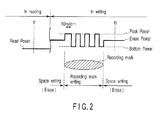
- FIG. 2 shows an example of laser emission power in a data read operation and a data write operation.
- the laser diode 79 repeats peak power and bottom power as shown in FIG. 2, thereby forming a recording mark on a track.
- the laser diode 79 generates erase power, thereby crystallizing the recording layer of the disc 100 to form a space (or to erase the mark).
- the laser diode 79 In a data read operation, the laser diode 79 generates read power continuously.
- the read power is much lower than the erase power and therefore the phase state of the recording layer is not changed by the read power.
- FIG. 3 is a block diagram showing the configuration of an embodiment of the laser control circuit 75.
- the peak reference current IPref corresponds to the target peak power of the LD 79.
- a current amplifier 23 amplifies the peak reference current IPref and outputs a peak current IP.
- the input voltage of the current amplifier 23 corresponds to the peak current value and is input via a switch SW5 to an ADC 18, which AD-converts the voltage.
- the resulting signal is read by the CPU 90.
- a switch SW1 goes on at the peak of the recording signal waveform in a write operation as shown in FIG. 2.
- the peak current IP amplified by the current amplifier 23 flows through the LD via an adder 27.
- An erase DAC 13 DA-converts erase reference data DEref set by the CPU 90 and outputs an erase reference current IEref.
- the erase reference current IEref shows target erase power.
- a sample hold circuit 12 samples the erase power with such timing as time te in generating the erase power in FIG. 2 and outputs an erase sample voltage VEsh to an erase auto-power controller (APC) 19.
- the erase sample voltage VEsh is input via the switch SM5 to the ADC 18, which AD-converts the voltage.
- the resulting signal is read by the CPU 90.
- the erase sample voltage VEsh shows emission power in an erase operation.
- An erase APC 19 converts the erase reference current IEref into an erase reference voltage VEref and compares the voltage with the erase sample voltage VEsh.
- the erase APC 19 outputs an erase current IEa APC-controlled so that VEref and VEsh may equal each other. For example, if the erase sample voltage VEsh is lower than the erase reference voltage VEref, the output erase current IEa is increased. Conversely, if the erase sample voltage VEsh is higher than the erase reference voltage VEref, the output erase current IEa is decreased.
- the current amplifier 24 amplifies the erase current IEa and outputs an erase current IE.
- the input voltage of the current amplifier 24 shows the magnitude of the erase current IEa.
- the input voltage of the current amplifier 24 is input via the switch SW5 to the ADC 18, which AD-converts the voltage.
- the resulting voltage is read by the CPU 90.
- the switch SW2 goes on during the erase period of the recoding signal waveform in a write operation as shown in FIG. 2.
- the erase current IP amplified by the current amplifier 24 flows through the LD via an adder 28 and the adder 27.
- the read reference current IRref shows target read power.
- a low-pass filter 14 filters the voltage generated by the output current Ifm of the front monitor FM.
- a sample hold circuit 15 samples the output value of an LFP 14 with such timing as time tr in generating the read power in FIG. 2 and outputs a read sample voltage VRsh to a read APC 21.
- the read sample voltage VRsh shows emission power in a read operation.
- a read APC 21 converts the read reference current IRref into a read reference voltage VRref and compares the voltage with the read sample voltage VRsh.
- the read APC 21 outputs a read current IRa APC-controlled so that the read reference voltage VRref and the read sample voltage VRsh may equal each other. For example, if the read sample voltage VRsh is lower than the read reference voltage VRref, the read current IRa is increased. Conversely, if the read sample voltage VRsh is higher than the read reference voltage VRref, the read current IRa is decreased.
- the current amplifier 25 amplifies the read current IRa and outputs a read current IR.
- the switch SW3 goes on in a read operation as shown in FIG. 2.
- the read current IR amplified by the current amplifier 25 flows through the LD via an adder 29 and the adders 28 and 27.
- the low-pass filter 14 and sample hold circuit 15 output an average value VAsh corresponding to average power P AVG in a write operation as shown in FIG. 5.
- the average value VAsh is input via the switch SW5 to the ADC 18, which AD-converts the average value.
- the resulting signal is read by the CPU 90.
- the switch SW3 remains off in a write operation.
- the bottom reference current IBref corresponds to target bottom power.
- a current amplifier 26 amplifies the bottom reference current IBref and outputs a bottom current IB.
- a switch SW4 goes on at the bottom level of the recording signal waveform in a write operation as shown in FIG. 2. As a result, the bottom current IB amplified by the current amplifier 26 flows through the LD via the adders 29, 28, 27.
- FIG. 4 shows the relationship between emission power used in LD emission power control and LD driving currents.
- the quality of a recording mark (or reproduced signal quality) formed in the recording layer of an optical disc depends greatly on the accuracy of the peak power of the LD. Therefore, it is necessary to control the peak power accurately so as to coincide with a target value.
- the emission power of the LD was measured with a light-receiving element, such as a front monitor, and a peak current for generating target power was determined.
- a peak current for generating target power was determined.
- the output current or output voltage of the light-receiving element in generating peak power was held at the peak hold circuit.
- the held value was AD-converted.
- the resulting signal was read by the CPU.
- a faster-response, higher-accuracy peak hold circuit was required. Use of such a peak hold circuit results in an increase in the manufacturing cost of the optical disc apparatus. The same holds true for bottom power.
- the current-to-emission-power characteristic of the LD is estimated in an embodiment of the invention and, on the basis of the current-to-emission-power characteristic, for example, the optimum peak current (or peak reference data DPref) is determined.
- the current-to-emission-power characteristic of the LD can be estimated.
- the current-to-emission-power characteristic of the LD is estimated. As seen from FIG. 2 and FIG. 5 described later, the measurement of the average power and erase power needs neither a fast-response sample hold circuit nor a front monitor.
- the erase APC 19 performs feedback control of the power sampled in a space interval by the sample hold circuit 12 so that the sample power may be equal to the target erase power, thereby controlling the erase power. In this way, the current value of the LD emitting light with the target erase power is acquired via an AD converter 18.
- the peak power can be determined almost uniquely from the I-L characteristic found from the average emission power, erase power, and pulse waveform. If the average power is close to the erase power, the waveform of the multi-pulse, average power, or erase power is changed temporarily and the I-L characteristic is estimated.
- FIG. 5 shows a conceptual diagram of average power. The high-frequency components are removed from the output of the front monitor FM by the low-pass filter 14 and the resulting signal is sampled by the sample hold circuit 15. The average power is obtained via the AD converter 18 from the sampled signal.
- FIG. 6 shows a waveform of a single pulse.
- FIG. 7 shows a waveform of a multi-pulse.
- the write strategy is a laser modulation method or a recording waveform in recording a mark onto an optical disc. It is defined for each length of a recording mark, such as 3T or 4T, in written standards or the like.
- Tsfp is the time from the rising of a write pulse signal (Write Pulse) until the first rising of a reference clock signal (CLOCK) when a data signal (DATA) is at the high (H) level.
- ⁇ and ⁇ are calculated by substituting dp', d E ', and d B ' into dp, d E , and d B in equation (2) and equation (3). If the frequency of appearance of each mark length and each space length in user data to be written is known, weighting can be done in calculating an average duty ratio.
- the I-L characteristic of the LD is nonlinear at high temperature and high output as shown in FIG. 8. At such high temperature and high output, the nonlinearity of the I-L characteristic can be compensated for by a method described below.
- FIG. 9 is a diagram to help explain a method of compensating for the current-to-emission-power nonlinear characteristic according to an embodiment of the invention.
- State 1 shows the I-L characteristic in the preceding sampling
- state 2 shows the I-L characteristic in the present sampling
- state 2' shows the I-L characteristic with no deviation from a straight line.
- the amount of deviation ⁇ P P from the straight line in the peak power is determined.
- FIG. 10 is a flowchart to help explain an LD driving current value setting process in laser emission power control. Each block is executed under the control of the CPU 90.
- the CPU 90 sets predetermined initial power (in FIG. 3, the individual initial values of the peak reference data DPref, erase reference data DEref, and bottom reference data DBref) or the power in the preceding start-up in the DAC 11, DAC 13, and DAC 17 (001)
- the pulse duty ratio of each of the bottom power, erase power, and peak power is calculated using equation (13) to equation (21) (002).
- a recording start trigger (instruction) is waited for (003).
- the erase power in FIG. 3, the output voltage VEsh of the sample hold circuit 12
- erase current the output terminal voltage of the erase APC 19
- a smoothing process such as taking a moving average, may be performed.
- the moving average is obtained by measuring the erase power and erase current repeatedly through a loop process and striking an average of the latest erase power and erase current.
- the erase APC 19 performs control so that the erase power may be kept at the target value.
- the output voltage (VAsh in FIG. 3) of the sample hold circuit 15 in recording is acquired as the average power P AVG from the ADC 18 (005).
- the average power P AVG is compared with the erase power obtained in block 004. If the difference between the average power and the erase power is equal or less than a specific value (or if the average power is close to the erase power) (Yes in 006), the waveform is changed temporarily in the direction of time or in the direction of amplitude, that is, the strategy is changed (012).
- the specific value of the difference is several % (e.g., 2%) of the difference between the peak power and bottom power.
- a case where the difference between the average power and the erase power is equal to or lees than the specific value is actually rare.
- the pulse duty ratio of each of the bottom power, erase power, and peak power is calculated again using equation (13) to equation (21) (002). Then, it is determined whether the erase power is almost equal to the average power (004 to 006). The above processes are repeated until the difference between the erase power and the average power has exceeded the specific value.
- the peak current value and bottom current value for causing the LD to emit light with a desired peak power and bottom power are calculated using equation (22) and equation (23) (007). Then, the calculated current values are set in the peak DAC 11 and bottom DAC 17 as current command values (in FIG. 3, the peak reference data DPref and bottom reference data DBref) (009). Thereafter, control returns to block 004, where a loop process is carried out periodically, which enables the emission power to be controlled.
- FIG. 11 is a flowchart to help explain an LD driving current value setting process in laser emission power control according to the second embodiment. Each block is executed under the control of the CPU 90.
- the linearity can be compensated for by performing control as shown in FIG. 11.
- the processes from the initial setting (101) to the acquisition of the average power (104) are the same as the above processes (001 to 004).
- an ambient temperature is estimated from the erase power setting value (in FIG. 3, the erase reference value DEref) and erase current (in FIG. 3, the current IEa).
- the erase power setting value in FIG. 3, the erase reference value DEref
- the current IEa the current IEa
- the erase APC 19 performs this control.
- the ambient temperature is estimated.
- the estimation of the ambient temperature in block 105 is for determining the timing of starting the compensation in the second embodiment and therefore it is not necessary to always perform control including compensation (107 to 109).
- the ambient temperature is higher than T1°C (in the case of an LD for DVD, about 50°C). If the ambient temperature is higher than T1°C (in the case of Yes), the I-L characteristic ( ⁇ , ⁇ ) in the straight line area is calculated using equations (27) and (28) (107). In block 108, the amount of deviation ⁇ Pp from the straight line at the peak power is found using equation (32). Finally, in block 109, the peak current and bottom current used in the present sampling interval are calculated using equations (33) and (34) and are set in the peak DAC 11 and bottom DAC 17, respectively.
- the I-L characteristic ( ⁇ , ⁇ ) is calculated by the method in block 007 to block 010 in the above-described flowchart of FIG. 10. Then, the resulting values are set in the peak DAC 11 and bottom DAC 17, respectively.
Landscapes
- Physics & Mathematics (AREA)
- Optics & Photonics (AREA)
- Optical Head (AREA)
- Optical Recording Or Reproduction (AREA)
Abstract
In a data write operation, the average value of the emission power detected by a front monitor (FM) is obtained via a low-pass filter (14) and a sample hold circuit (15). In the write operation, erase power controlled by an erase APC (19) is obtained via a sample hold circuit (12). While an LD (79) is emitting light with the erase power, an erase current is determined from the output voltage of the erase APC (19). On the basis of the average power, the erase power, the erase current, and a waveform of the recording pulse, a current-to-emission-power characteristic of the LD (79) is estimated (007). Furthermore, on the basis of the current-to-emission-power characteristic, the peak power in the write operation of the LD (79) are controlled (008 to 010).
Description
- This invention relates to the technique for recording information onto a recordable optical disc, such as CD-R, CD-RW, DVD-R, DVD-RW, DVD-RAM, HDDVD-R, HDDVD-RAM, or HDDVD-RW, and more particularly to control of recording power.
- In recent years, a high recording density optical disc apparatus, such as a DVD recorder, has been popularized. With improvements in the recording density of the optical disc, the optical disc has been required to have a high reliability of its recoding quality.
- For example, in a rewritable optical disc, groove and/or land tracks are formed on the disc surface, recording layers are formed at the tracks, and a beam spot of laser light is caused to follow a track, thereby forming or erasing recording marks. It is known that the driving-current-to-emission-power characteristic of a laser diode used for an optical disc fluctuates according to temperature change or temporal change. To improve the recording performance, it is important to control the emission power so that the power may be constant.
- In a conventional power control method, first, the value of recording power (peak power) in the mark part, the value of recording power (erase power) in the space part, and the value of bottom power in a multi-pulse are held. Then, on the basis of the held values and the ratio of the erase power to preset peak power and bottom power, erase power is calculated. The recording pulse is controlled so that the actual intensity levels of the peak power, bottom power, and erase power may coincide with respective target values (Jpn. Pat. Appln. KOKAI Publication
No. 2000-30276 - Generally, control to keep the emission power of a laser diode (LD) constant (Auto Power Control, hereinafter referred to as APC) is performed on the three levels, peak power, erase power, and bottom power, in a multi-pulse method of recording a single recording mark with a plurality of peak power pulses by use of a peak (bottom) hold circuit and a sample hold circuit through analog or digital feedback control. The conventional method, however, has the following problems:
- (1) A fast-response/high-accuracy peak hold circuit or sample hold circuit is required.
- (2) When pulses (boost pulses) higher than those in the other parts are used only as the pulses corresponding to the beginning and end of a mark part, it is unclear which one of a plurality of peak levels is held by the peak hold circuit.
- (3) As an optical monitor element, such as a front monitor, to measure a peak level, a broadband one is needed.
- These problems arise prominently as the recording density and speed of the optical disc increase.
- It is, accordingly, an object of the invention to provide control whereby an LD is caused to always emit light with required power without using a high-priced fast response/high accuracy peak hold circuit or broadband monitor, even if a fluctuation in the characteristic of the LD occurs due to temperature changes.
- To solve the problems in the conventional method, there is provided a method of estimating the current-to-emission-power characteristic (hereinafter, referred to as the I-L characteristic) of an LD using the average power and erase power in recording that can be measured with a narrowband peak hold circuit without using a broadband peak hold circuit and determining a current setting value to obtain an arbitrary power level.
- Since the I-L characteristic fluctuates due to temperature changes or time degradation, it is necessary to determine a driving current value that causes the optimum power to be generated constantly. At this time, if the latest I-L characteristic is known, not only can a constant emission level be kept, but also a current value to obtain a new target level can be known immediately, even when the target level is changed in learning or testing the write characteristic. Therefore, it is possible to control the emission power level instantaneously without going through transitional conditions in feedback control of conventional emission power.
- According to an embodiment of the invention, it is possible to provide control whereby an LD is caused to always emit light with required power without using a high-priced fast response/high accuracy peak hold circuit or broadband monitor, even if the characteristic of the LD fluctuates due to temperature changes.
- The invention can be more fully understood from the following detailed description when taken in conjunction with the accompanying drawings, in which:
- FIG. 1 is a block diagram showing an example of the configuration of an optical disc apparatus to which the invention is applied;
- FIG. 2 is a diagram to help explain an example of laser emission power in a data read operation and a data write operation;
- FIG. 3 is a block diagram showing the configuration of an embodiment of the laser control circuit;
- FIG. 4 shows the relationship between emission power used in LD emission power control and LD driving currents;
- FIG. 5 is a diagram to help explain average power;
- FIG. 6 is a diagram to help explain the duty ratio of a single-pulse recording waveform;
- FIG. 7 is a diagram to help explain the duty ratio of a multi-pulse recording waveform;
- FIG. 8 is a graph obtained when the current to emission power of a laser diode is nonlinear;
- FIG. 9 is a graph to help explain an embodiment of a method of compensating for the nonlinear characteristic of the current to emission power in the invention;
- FIG. 10 is a flowchart to help explain an LD driving current value setting process in laser emission power control; and
- FIG. 11 is a flowchart to help explain a second embodiment of the LD driving current value setting process in laser emission power control.
- Hereinafter, referring to the accompanying drawings, embodiments of the present invention will be explained.
- FIG. 1 is a block diagram showing an example of the configuration of an optical disc apparatus to which the invention is applied.
- The optical disc apparatus records and reproduces information onto and from an information storage medium, or an
optical disc 100, such as a DVD (Digital Versatile Disc). In theoptical disc 100, grooves are cut concentrically or spirally. The concave parts are called lands and the convex parts are called grooves. One round of a groove or a land is called a track. Intensity-modulated laser light is applied along the track (or only a groove or both a groove and a land) to form recording marks, thereby recording user data. The data is reproduced by applying read-power laser light weaker than in recording to the track and detecting changes in the reflected light intensity caused by recording marks on the track. The recorded data is erased by applying erase-power laser light higher than the read power to the track to crystallize the recording layer. - The
optical disc 100 is rotated by aspindle motor 63. Arotation detector 63a provided on thespindle motor 63 supplies FG pulses. When thespindle motor 63 makes one revolution, for example, five FG pulses are generated. From the FG pulses, the rotation angle and rotation number of thespindle motor 63 can be determined. - Information is recorded onto and reproduced from the
optical disc 100 by anoptical pickup 65. Theoptical pickup 65 is coupled with asled motor 66 via a gear. Thesled motor 66 is controlled by a sledmotor control circuit 68. - A
speed detecting circuit 69 is connected to the sledmotor control circuit 68. A speed signal of theoptical pickup 65 detected by thespeed detecting circuit 69 is sent to the sledmotor control circuit 68. A permanent magnet (not shown) is provided at the fixed part of thesled motor 66. Adriving coil 67 is excited by the sledmotor control circuit 68, thereby moving theoptical pickup 65 over the radius of theoptical disc 100. - An
objective lens 70 supported by a wire or leaf spring (not shown) is provided to theoptical pickup 65. Theobjective lens 70 can be moved by the driving of adriving coil 72 in the focusing direction (or in the direction of optical axis of the lens). It also can be moved by the driving of adriving coil 71 in the tracking direction (or in the direction perpendicular to the optical axis of the lens). - A
modulation circuit 73 subjects user data supplied from ahost unit 94 via aninterface circuit 93 to, for example, 8-14 modulation (EFM) in recording information, thereby providing EFM data. When information is recorded (or when a mark is formed), alaser control circuit 75 supplies a write signal to a laser diode (or laser light-emitting element) 79 on the basis of the EFM data supplied from themodulation circuit 73. When information is read, thelaser control circuit 75 supplies a read signal smaller than the write signal to thelaser diode 79. The configuration of thelaser control circuit 75 will be described in detail later. - A front monitor FM composed of a photodiode detects the light quantity of laser light, or emission power, generated by the
laser diode 79 and supplies the detected current to thelaser control circuit 75. On the basis of the detected current from the front monitor FM, thelaser control circuit 75 controls thelaser diode 79 so as to cause thediode 79 to emit light with reproducing laser power, recording laser power, or erasing laser power set by aCPU 90. - The
laser diode 79 generates laser light according to the signal supplied from thelaser control circuit 75. The laser light emitted from thelaser diode 79 passes through acollimator lens 80, ahalf prism 81, and theobjective lens 70 and is shed on theoptical disc 100. The reflected light from theoptical disc 100 passes through theobjective lens 70,half prism 81, a condenser lens 82, and acylindrical lens 83 and is directed to anphotodetector 84. - The
photodetector 84 is composed of, for example, quadrant photo-detection cells. The detected signals of these photo-detection cells are output to anRF amplifier 85. TheRF amplifier 85 processes the signals from the photo-detection cells and produces a focus error signal FE indicating a deviation from the just focus, a tracking error signal TE indicating the difference between the beam spot center of laser light and the track center, and an RF signal as the sum total signal of photo-detection cell signals. - The focus error signal FE is supplied to a focusing
control circuit 87. The focusingcontrol circuit 87 generates a focus driving signal according to a focus error signal FE. The focus driving signal is supplied to the drivingcoil 71 in the focusing direction. This achieves focus servo whereby laser light is caused to always focus on the recording film of theoptical disc 100. - The tracking error signal TE is supplied to a
tracking control circuit 88. Thetracking control circuit 88 generates a track driving signal according to the tracking error signal TE. The track driving signal output from thetracking control circuit 88 is supplied to the drivingcoil 72 in the tracking direction. This achieves tracking servo whereby laser light is caused to always trace a track formed on theoptical disc 100. - Use of the focus servo and tracking servo causes changes in the reflected light from the pits made in the track of the
optical disc 100 according to the recording information to be reflected in the sum total signal RF of the output signals of the individual photo-detection cells of thephotodetector 84. The signal is supplied to adata reproducing circuit 78. Thedata reproducing circuit 78 reproduces the recorded data on the basis of the reproducing clock signal from aPLL circuit 76. - When the
objective lens 70 is controlled by thetracking control circuit 88, the sledmotor control circuit 68 controls thesled motor 66 orPUH 65 in such a manner that theobjective lens 70 comes close to a specific position in thePUH 65. - The
motor control circuit 64, sledmotor control circuit 68,laser control circuit 73,PLL circuit 76,data reproducing circuit 78, focusingcontrol circuit 87, trackingcontrol circuit 88,error correction circuit 62, and others are controlled by theCPU 90 via thebus 89. According to an operation command supplied from ahost unit 94 via aninterface circuit 93, theCPU 90 controls the recording and reproducing apparatus in a comprehensive manner. TheCPU 90 uses aRAM 91 as a working area and performs a specific operation according to a control program including programs of the invention recorded in aROM 92. - FIG. 2 shows an example of laser emission power in a data read operation and a data write operation.
- In a data write operation, the
laser diode 79 repeats peak power and bottom power as shown in FIG. 2, thereby forming a recording mark on a track. Thelaser diode 79 generates erase power, thereby crystallizing the recording layer of thedisc 100 to form a space (or to erase the mark). - In a data read operation, the
laser diode 79 generates read power continuously. The read power is much lower than the erase power and therefore the phase state of the recording layer is not changed by the read power. - FIG. 3 is a block diagram showing the configuration of an embodiment of the
laser control circuit 75. - A
peak DAC 11 DA-converts peak reference data DPref set by theCPU 90 and outputs a peak reference current IPref. The peak reference current IPref corresponds to the target peak power of theLD 79. Acurrent amplifier 23 amplifies the peak reference current IPref and outputs a peak current IP. At this time, the input voltage of thecurrent amplifier 23 corresponds to the peak current value and is input via a switch SW5 to anADC 18, which AD-converts the voltage. The resulting signal is read by theCPU 90. A switch SW1 goes on at the peak of the recording signal waveform in a write operation as shown in FIG. 2. As a result, the peak current IP amplified by thecurrent amplifier 23 flows through the LD via anadder 27. - An erase
DAC 13 DA-converts erase reference data DEref set by theCPU 90 and outputs an erase reference current IEref. The erase reference current IEref shows target erase power. Asample hold circuit 12 samples the erase power with such timing as time te in generating the erase power in FIG. 2 and outputs an erase sample voltage VEsh to an erase auto-power controller (APC) 19. The erase sample voltage VEsh is input via the switch SM5 to theADC 18, which AD-converts the voltage. The resulting signal is read by theCPU 90. The erase sample voltage VEsh shows emission power in an erase operation. - An erase
APC 19 converts the erase reference current IEref into an erase reference voltage VEref and compares the voltage with the erase sample voltage VEsh. The eraseAPC 19 outputs an erase current IEa APC-controlled so that VEref and VEsh may equal each other. For example, if the erase sample voltage VEsh is lower than the erase reference voltage VEref, the output erase current IEa is increased. Conversely, if the erase sample voltage VEsh is higher than the erase reference voltage VEref, the output erase current IEa is decreased. - The
current amplifier 24 amplifies the erase current IEa and outputs an erase current IE. The input voltage of thecurrent amplifier 24 shows the magnitude of the erase current IEa. Moreover, the input voltage of thecurrent amplifier 24 is input via the switch SW5 to theADC 18, which AD-converts the voltage. The resulting voltage is read by theCPU 90. The switch SW2 goes on during the erase period of the recoding signal waveform in a write operation as shown in FIG. 2. As a result, the erase current IP amplified by thecurrent amplifier 24 flows through the LD via anadder 28 and theadder 27. - A
read DAC 16 DA-converts read reference data DRref set by theCPU 90 and outputs a read reference current IRref. The read reference current IRref shows target read power. A low-pass filter 14 filters the voltage generated by the output current Ifm of the front monitor FM. Asample hold circuit 15 samples the output value of anLFP 14 with such timing as time tr in generating the read power in FIG. 2 and outputs a read sample voltage VRsh to aread APC 21. The read sample voltage VRsh shows emission power in a read operation. - A
read APC 21 converts the read reference current IRref into a read reference voltage VRref and compares the voltage with the read sample voltage VRsh. Theread APC 21 outputs a read current IRa APC-controlled so that the read reference voltage VRref and the read sample voltage VRsh may equal each other. For example, if the read sample voltage VRsh is lower than the read reference voltage VRref, the read current IRa is increased. Conversely, if the read sample voltage VRsh is higher than the read reference voltage VRref, the read current IRa is decreased. - The
current amplifier 25 amplifies the read current IRa and outputs a read current IR. The switch SW3 goes on in a read operation as shown in FIG. 2. As a result, the read current IR amplified by thecurrent amplifier 25 flows through the LD via anadder 29 and theadders - The low-
pass filter 14 and sample holdcircuit 15 output an average value VAsh corresponding to average power PAVG in a write operation as shown in FIG. 5. The average value VAsh is input via the switch SW5 to theADC 18, which AD-converts the average value. The resulting signal is read by theCPU 90. The switch SW3 remains off in a write operation. - A
bottom DAC 17 DA-converts bottom reference data DBref set by theCPU 90 and outputs a bottom reference current IBref. The bottom reference current IBref corresponds to target bottom power. Acurrent amplifier 26 amplifies the bottom reference current IBref and outputs a bottom current IB. A switch SW4 goes on at the bottom level of the recording signal waveform in a write operation as shown in FIG. 2. As a result, the bottom current IB amplified by thecurrent amplifier 26 flows through the LD via theadders - Next, a concrete method of estimating the I-L characteristic will be described.
- FIG. 4 shows the relationship between emission power used in LD emission power control and LD driving currents. The quality of a recording mark (or reproduced signal quality) formed in the recording layer of an optical disc depends greatly on the accuracy of the peak power of the LD. Therefore, it is necessary to control the peak power accurately so as to coincide with a target value.
- Previously, while the magnitude of the peak current for generating the peak power was being changed, the emission power of the LD was measured with a light-receiving element, such as a front monitor, and a peak current for generating target power was determined. At this time, when emission power was measured, the output current or output voltage of the light-receiving element in generating peak power was held at the peak hold circuit. The held value was AD-converted. The resulting signal was read by the CPU. As the data recorded onto the optical disc got denser and the rotation number of the disc in recording increased, a faster-response, higher-accuracy peak hold circuit was required. Use of such a peak hold circuit results in an increase in the manufacturing cost of the optical disc apparatus. The same holds true for bottom power.
- To overcome this problem, the current-to-emission-power characteristic of the LD is estimated in an embodiment of the invention and, on the basis of the current-to-emission-power characteristic, for example, the optimum peak current (or peak reference data DPref) is determined.
- In FIG. 4, for example, if a straight line passing through the peak power (point B in FIG. 4) in peak-current driving and the erase power (point A in FIG. 4) in erase-current driving is known, the current-to-emission-power characteristic of the LD can be estimated. In the embodiment of the invention, using the average power measured value and erase power measured value in a write operation as parameters, the current-to-emission-power characteristic of the LD is estimated. As seen from FIG. 2 and FIG. 5 described later, the measurement of the average power and erase power needs neither a fast-response sample hold circuit nor a front monitor.
- First, the erase
APC 19 performs feedback control of the power sampled in a space interval by thesample hold circuit 12 so that the sample power may be equal to the target erase power, thereby controlling the erase power. In this way, the current value of the LD emitting light with the target erase power is acquired via anAD converter 18. - The peak power can be determined almost uniquely from the I-L characteristic found from the average emission power, erase power, and pulse waveform. If the average power is close to the erase power, the waveform of the multi-pulse, average power, or erase power is changed temporarily and the I-L characteristic is estimated. FIG. 5 shows a conceptual diagram of average power. The high-frequency components are removed from the output of the front monitor FM by the low-
pass filter 14 and the resulting signal is sampled by thesample hold circuit 15. The average power is obtained via theAD converter 18 from the sampled signal. - Hereinafter, concrete calculation examples will be described.
- If power is P and current is I, the I-L characteristic of the LD is expressed as equation (1):

- Using the average power measured value PAVG, erase power measured value PE, the duty ratios dP, dE, and dB of the peak pulse, erase pulse, and bottom pulse (dp + dE + dB = 1) respectively, and the respective current values Ip, IE, and IB, the coefficients α and β can be expressed by equation (2) and equation (3):


- Here, the duty ratios dp, dE, and dB (dp + dE + dB = 1) are constants determined by waveforms. FIG. 6 shows a waveform of a single pulse. FIG. 7 shows a waveform of a multi-pulse.
- In the case of NT space/NT mark consecutive pattern as shown in FIG. 6, if the data period is A, the erase width in one data period is K, the peak pulse width is M, and the bottom width is L (where N in NT is, for example, an integer in the range from 2 to 13 and T is a reference clock period), the duty ratios can be expressed by the following equations:


- When these are expressed using Tsfp and Telp in a write strategy, the following equations are obtained. The write strategy is a laser modulation method or a recording waveform in recording a mark onto an optical disc. It is defined for each length of a recording mark, such as 3T or 4T, in written standards or the like. For example, Tsfp is the time from the rising of a write pulse signal (Write Pulse) until the first rising of a reference clock signal (CLOCK) when a data signal (DATA) is at the high (H) level.


- In the case of a 2T multi-pulse NT space/NT mark consecutive pattern as shown in FIG. 7, if the data period is A, the peak pulse widths in one data period are B, C, and D, the erase width is E, and the bottom width is H, the duty ratios are expressed by the following equations:


- When these are expressed using Tsfp, Telp, Tefp, Tsmp, Temp, Tslp, and Tlc in the write strategy, the following equations are obtained:
- When N = 2,


- When N ≥ 3,


- In actual data, suppose each mark length and each space length appear evenly. If the shortest mark length is Tmin [T] and the longest mark length is Tmax [T], let


- Then, α and β are calculated by substituting dp', dE', and dB' into dp, dE, and dB in equation (2) and equation (3). If the frequency of appearance of each mark length and each space length in user data to be written is known, weighting can be done in calculating an average duty ratio.
- Peak current IP and bottom current IB corresponding to the target peak power PP and bottom power PB are found using equation (1) as follows:


- Repeating the above estimating process at a constant frequency makes it possible to always obtain the latest I-L characteristic and control the power level even in the middle of recording user data onto the optical disc.
- It is known that the I-L characteristic of the LD is nonlinear at high temperature and high output as shown in FIG. 8. At such high temperature and high output, the nonlinearity of the I-L characteristic can be compensated for by a method described below.
- FIG. 9 is a diagram to help explain a method of compensating for the current-to-emission-power nonlinear characteristic according to an embodiment of the invention.
State 1 shows the I-L characteristic in the preceding sampling,state 2 shows the I-L characteristic in the present sampling, and state 2' shows the I-L characteristic with no deviation from a straight line. - If the coefficients used in calculating the peak current and bottom current in the preceding sampling interval are α' and β' and the coefficients in the present sampling intervals are α and β, the I-L characteristic in a straight line area is expressed by the following equations:


- Since α and β represent the present state, the following equation holds:

- Here, since α hardly changes even if the temperature changes, α can be approximated as follows:

- Thus, β is found using the following equation:

- Moreover, the amount of deviation ΔPP from the straight line in the peak power is determined.
- If the peak current is IP' and bottom current is IB' in the preceding sampling interval and ΔPP is taken into consideration, the peak power Pp and bottom power PB are expressed by the following equations:


- Using the duty ratios dp, dE, and dB, the average power PAVG obtained from an AD converter is expressed by the following equation:

- Substituting equations (29) and (30) into equation (31) gives:

- In this way, ΔPp from the straight line is determined.
- Finally, the peak current IP and bottom current IB used in the present sampling interval are calculated.
- If the peak power and bottom power necessary for recording are Ppref and PBref respectively, the peak current Ip and bottom current IB can be determined as follows:


- Even if the I-L characteristic is nonlinear, use of the above method makes it possible to compensate for the nonlinearity.
- Next, a recording power control operation according to an embodiment of the invention will be explained in detail. FIG. 10 is a flowchart to help explain an LD driving current value setting process in laser emission power control. Each block is executed under the control of the
CPU 90. - First, the
CPU 90 sets predetermined initial power (in FIG. 3, the individual initial values of the peak reference data DPref, erase reference data DEref, and bottom reference data DBref) or the power in the preceding start-up in theDAC 11,DAC 13, and DAC 17 (001) - From the present write strategy, the pulse duty ratio of each of the bottom power, erase power, and peak power is calculated using equation (13) to equation (21) (002). A recording start trigger (instruction) is waited for (003). If recording is started, the erase power (in FIG. 3, the output voltage VEsh of the sample hold circuit 12) and erase current (the output terminal voltage of the erase APC 19) are taken in as digital signals via the AD converter 18 (004). Here, a smoothing process, such as taking a moving average, may be performed. The moving average is obtained by measuring the erase power and erase current repeatedly through a loop process and striking an average of the latest erase power and erase current. At this time, the erase
APC 19 performs control so that the erase power may be kept at the target value. - The output voltage (VAsh in FIG. 3) of the
sample hold circuit 15 in recording is acquired as the average power PAVG from the ADC 18 (005). The average power PAVG is compared with the erase power obtained inblock 004. If the difference between the average power and the erase power is equal or less than a specific value (or if the average power is close to the erase power) (Yes in 006), the waveform is changed temporarily in the direction of time or in the direction of amplitude, that is, the strategy is changed (012). Here, the specific value of the difference is several % (e.g., 2%) of the difference between the peak power and bottom power. Here, a case where the difference between the average power and the erase power is equal to or lees than the specific value is actually rare. - From the changed strategy, the pulse duty ratio of each of the bottom power, erase power, and peak power is calculated again using equation (13) to equation (21) (002). Then, it is determined whether the erase power is almost equal to the average power (004 to 006). The above processes are repeated until the difference between the erase power and the average power has exceeded the specific value.
- The erase power, erase current, and average power obtained in
block 004 and block 005, the peak current and bottom current set inblock 001, and each pulse duty ratio calculated inblock 002 are substituted into equation (2) and equation (3), thereby estimating the current-to-output characteristic of the laser diode (α and β). As the peak current and bottom current, IPref and IBref in FIG. 3 may be obtained viaADC 18. Since these values are practically the same as those set inblock 001, the values set inblock 001 are used. - From the estimated current-to-output characteristic, the peak current value and bottom current value for causing the LD to emit light with a desired peak power and bottom power are calculated using equation (22) and equation (23) (007). Then, the calculated current values are set in the
peak DAC 11 andbottom DAC 17 as current command values (in FIG. 3, the peak reference data DPref and bottom reference data DBref) (009). Thereafter, control returns to block 004, where a loop process is carried out periodically, which enables the emission power to be controlled. - Next, a recording power control operation according to a second embodiment of the invention will be explained. FIG. 11 is a flowchart to help explain an LD driving current value setting process in laser emission power control according to the second embodiment. Each block is executed under the control of the
CPU 90. - For example, if the I-L characteristic of a red LD is nonlinear at high temperature and high output as described above, the linearity can be compensated for by performing control as shown in FIG. 11. The processes from the initial setting (101) to the acquisition of the average power (104) are the same as the above processes (001 to 004).
- In block 105, an ambient temperature is estimated from the erase power setting value (in FIG. 3, the erase reference value DEref) and erase current (in FIG. 3, the current IEa). When light has been emitted with high emission power and the ambient temperature has become high, the luminous efficiency of the LD drops. Therefore, to emit light even at high temperature with the same power as at normal temperature, the current value has to be increased. The erase
APC 19 performs this control. On the basis of an increment in the current at this time, the ambient temperature is estimated. The estimation of the ambient temperature in block 105 is for determining the timing of starting the compensation in the second embodiment and therefore it is not necessary to always perform control including compensation (107 to 109). - In
block 106, it is determined whether the ambient temperature is higher than T1°C (in the case of an LD for DVD, about 50°C). If the ambient temperature is higher than T1°C (in the case of Yes), the I-L characteristic (α, β) in the straight line area is calculated using equations (27) and (28) (107). Inblock 108, the amount of deviation ΔPp from the straight line at the peak power is found using equation (32). Finally, in block 109, the peak current and bottom current used in the present sampling interval are calculated using equations (33) and (34) and are set in thepeak DAC 11 andbottom DAC 17, respectively. - In
block 106, if the ambient temperature is equal to or lower than T1°C (in the case of No), the I-L characteristic (α, β) is calculated by the method inblock 007 to block 010 in the above-described flowchart of FIG. 10. Then, the resulting values are set in thepeak DAC 11 andbottom DAC 17, respectively. - As described above, according to the embodiments of the invention, it is possible to provide control whereby an LD always emits light with required power without using a high-priced fast-response/high-accuracy peak hold circuit or broadband monitor even if the characteristic of the LD fluctuates due to temperature changes.
Claims (10)
- An optical disc apparatus characterized by comprising:a laser light-emitting element;a detecting unit (FM) which detects the emission power of the laser light-emitting element;an average power measuring unit (14, 15) which measures an average value of the emission power detected by the detecting unit in a write operation in which the laser light-emitting element is driven with recording pulses and marks are formed on a track on an optical disc;an erase power measuring unit (12, 18) which, in the write operation, measures erase power controlled so as to coincide with a target value by feedback control;an erase current measuring unit (19, 18) which, while the laser light-emitting element is emitting light with the erase power, measures an erase current driving the laser light-emitting element;an estimating unit (80, 007) which estimates a current-to-emission-power characteristic of the laser light-emitting element on the basis of the average power, the erase power, the erase current, and a waveform of the recording pulse; andcontrol unit (90, 008 to 010) which controls the peak power of the laser light-emitting element in the write operation on the basis of the current-to-emission-power characteristic.
- The optical disc apparatus according to claim 1, characterized in that the estimating unit estimates the current-to-emission-power characteristic to be a straight line and further estimates the amount of deviation of actually generated peak power from target peak power in the write operation calculated from the current-to-emission-power characteristic (108), and
the control units correct the actually generated peak power on the basis of the amount of deviation (107). - The optical disc apparatus according to claim 1 or 2, characterized by further comprising a unit (012) which, when the difference between the average power and the erase power is equal to or less than a specific value, changes a write strategy of the recording pulse waveform.
- The optical disc apparatus according to any one of claim 1 to claim 3, characterized in that the control unit controls the bottom power of the laser light-emitting element in the write operation on the basis of the current-to-emission-power characteristic (17, 18).
- A recording power control method characterized by comprising the steps of:detecting the emission power of a laser light-emitting element (FM), and measuring an average value of the detected emission power (005, 15) in a write operation in which the laser light-emitting element is driven with recording pulses and marks are formed on a track on an optical disc;in the write operation, measuring erase power controlled so as to coincide with a target value by feedback control (004, 12);while the laser light-emitting element is emitting light with the erase power, measuring an erase current driving the laser light-emitting element (004, 12);estimating a current-to-emission-power characteristic of the laser light-emitting element on the basis of the average power, the erase power, the erase current, and a waveform of the recording pulse (007); andcontrolling the peak power of the laser light-emitting element in the write operation on the basis of the current-to-emission-power characteristic.
- The recording power control method according to claim 5, characterized in that the step of estimating the current-to-emission-power characteristic includes a step of estimating the current-to-emission-power characteristic to be a straight line and further estimating the amount of deviation ΔPP of actually generated peak power from target peak power in the write operation calculated from the current-to-emission-power characteristic (108), and
the step of controlling the peak power includes a step of correcting the actually generated peak power on the basis of the amount of deviation ΔPP (109). - The recording power control method according to claim 5, characterized by further comprising a step of, when the difference between the average power and the erase power is equal to or less than a specific value, changing a write strategy of the recording pulse waveform.
- The recording power control method according to claim 6, characterized by further comprising a step of, when the difference between the average power and the erase power is equal to or less than a specific value, changing a write strategy of the recording pulse waveform.
- The recording power control method according to claim 5, characterized in that the step of controlling the peak power includes a step of controlling the bottom power of the laser light-emitting element in the write operation on the basis of the current-to-emission-power characteristic.
- The recording power control method according to claim 6, characterized in that the step of controlling the peak power includes a step of controlling the bottom power of the laser light-emitting element in the write operation on the basis of the current-to-emission-power characteristic.
Applications Claiming Priority (1)
| Application Number | Priority Date | Filing Date | Title |
|---|---|---|---|
| JP2006152758A JP2007323734A (en) | 2006-05-31 | 2006-05-31 | Optical disc apparatus and recording power control method |
Publications (1)
| Publication Number | Publication Date |
|---|---|
| EP1863023A2 true EP1863023A2 (en) | 2007-12-05 |
Family
ID=38442629
Family Applications (1)
| Application Number | Title | Priority Date | Filing Date |
|---|---|---|---|
| EP07109206A Withdrawn EP1863023A2 (en) | 2006-05-31 | 2007-05-30 | Optical disc apparatus and recording power control method |
Country Status (6)
| Country | Link |
|---|---|
| US (1) | US20080144453A1 (en) |
| EP (1) | EP1863023A2 (en) |
| JP (1) | JP2007323734A (en) |
| KR (1) | KR100892331B1 (en) |
| CN (1) | CN101083094A (en) |
| TW (1) | TW200818147A (en) |
Families Citing this family (2)
| Publication number | Priority date | Publication date | Assignee | Title |
|---|---|---|---|---|
| JP2008299957A (en) * | 2007-05-31 | 2008-12-11 | Toshiba Corp | Optical disk device and method for controlling optical disk device |
| US20100272139A1 (en) * | 2009-04-23 | 2010-10-28 | Mediatek Inc. | Driving circuit for driving laser diode and method for controlling laser powers of laser diode |
Family Cites Families (9)
| Publication number | Priority date | Publication date | Assignee | Title |
|---|---|---|---|---|
| JP3441212B2 (en) * | 1995-01-19 | 2003-08-25 | 株式会社リコー | Power control method |
| JP3457463B2 (en) * | 1996-04-26 | 2003-10-20 | 富士通株式会社 | Optical storage |
| KR20010003547A (en) * | 1999-06-24 | 2001-01-15 | 윤종용 | Method for detecting of optimum writing power in a optic disk |
| JP3697962B2 (en) * | 1999-08-20 | 2005-09-21 | ティアック株式会社 | Optical disk drive device |
| JP2004110915A (en) * | 2002-09-17 | 2004-04-08 | Ricoh Co Ltd | Write power control method and device |
| JP2004318996A (en) * | 2003-04-16 | 2004-11-11 | Sanyo Electric Co Ltd | Optical disk device and control method thereof |
| JP4145713B2 (en) * | 2003-05-19 | 2008-09-03 | 株式会社リコー | LASER POWER CONTROL DEVICE, INFORMATION RECORDING DEVICE, OPTICAL DISK DEVICE, LASER LIGHT SOURCE DRIVE CURRENT DETERMINING METHOD, INFORMATION RECORDING METHOD, AND OPTICAL DISK RECORDING METHOD |
| US20050083828A1 (en) * | 2003-10-17 | 2005-04-21 | Chih-Yuan Chen | Apparatus and method for laser power control |
| JP2005202995A (en) * | 2004-01-13 | 2005-07-28 | Matsushita Electric Ind Co Ltd | Light emitting current adjusting method for optical disc apparatus and optical disc apparatus |
-
2006
- 2006-05-31 JP JP2006152758A patent/JP2007323734A/en not_active Withdrawn
-
2007
- 2007-05-29 KR KR1020070052039A patent/KR100892331B1/en not_active Expired - Fee Related
- 2007-05-30 EP EP07109206A patent/EP1863023A2/en not_active Withdrawn
- 2007-05-30 TW TW096119386A patent/TW200818147A/en unknown
- 2007-05-31 CN CNA2007101059110A patent/CN101083094A/en active Pending
- 2007-05-31 US US11/809,164 patent/US20080144453A1/en not_active Abandoned
Also Published As
| Publication number | Publication date |
|---|---|
| CN101083094A (en) | 2007-12-05 |
| US20080144453A1 (en) | 2008-06-19 |
| KR100892331B1 (en) | 2009-04-08 |
| TW200818147A (en) | 2008-04-16 |
| KR20070115684A (en) | 2007-12-06 |
| JP2007323734A (en) | 2007-12-13 |
Similar Documents
| Publication | Publication Date | Title |
|---|---|---|
| US7212477B2 (en) | Optical recording/reproducing apparatus with APC and SPS processes | |
| US5712839A (en) | Laser light power control system having reflected light detector | |
| KR101162371B1 (en) | Laser driving method and laser driving device | |
| KR20030020932A (en) | Optical recorder and laser power control method | |
| JP3552938B2 (en) | Optical disk apparatus and correction method therefor | |
| WO2003001519A1 (en) | Information recording method and information recording apparatus | |
| US20020101806A1 (en) | Method of calculating write condition detection index and optical disk writing method and apparatus using the method | |
| US20040047255A1 (en) | Information recording apparatus and information recording method | |
| US20050083828A1 (en) | Apparatus and method for laser power control | |
| US20080144453A1 (en) | Optical disc apparatus and recording power control method | |
| US7126896B2 (en) | Information recording method, recording condition detection method, and information recording apparatus | |
| US20040013068A1 (en) | Information recording apparatus and method thereof, and waveform data generating device and method thereof | |
| US7239590B2 (en) | Write power control method, write power control apparatus and information recording apparatus having the same | |
| US20080069158A1 (en) | Laser power control technique and apparatus for recording and reproducing data in and from optical disk under laser power control | |
| US7170837B2 (en) | Optical disk device having means for generating a tracking offset signal according to laser diode current or temperature | |
| US7808871B2 (en) | Power control apparatus and method for an optical drive | |
| JP4209205B2 (en) | Light beam output control device, optical pickup device, light beam emission control method, light beam emission control program, and recording medium recording the same | |
| US20080101428A1 (en) | Laser-power control method, and laser driving device and optical disc apparatus using the method | |
| US20090180366A1 (en) | Optical disc recording apparatus | |
| US20080084805A1 (en) | Writing power calibrating method and data recording apparatus using the same | |
| JP4027886B2 (en) | Optical information recording / reproducing apparatus, laser light source driving current value determining method, program for executing the method, and computer-readable recording medium storing the program | |
| JP4726517B2 (en) | Optical information recording device | |
| JP2004110963A (en) | Laser control device | |
| JP2008300005A (en) | Optical disc apparatus and control method thereof | |
| JP2004199839A (en) | Optical disk recording device |
Legal Events
| Date | Code | Title | Description |
|---|---|---|---|
| PUAI | Public reference made under article 153(3) epc to a published international application that has entered the european phase |
Free format text: ORIGINAL CODE: 0009012 |
|
| 17P | Request for examination filed |
Effective date: 20070530 |
|
| AK | Designated contracting states |
Kind code of ref document: A2 Designated state(s): AT BE BG CH CY CZ DE DK EE ES FI FR GB GR HU IE IS IT LI LT LU LV MC MT NL PL PT RO SE SI SK TR |
|
| AX | Request for extension of the european patent |
Extension state: AL BA HR MK YU |
|
| STAA | Information on the status of an ep patent application or granted ep patent |
Free format text: STATUS: THE APPLICATION HAS BEEN WITHDRAWN |
|
| 18W | Application withdrawn |
Effective date: 20090610 |