EP1861905B1 - Polarization-reversed iii-nitride light-emitting device - Google Patents
Polarization-reversed iii-nitride light-emitting device Download PDFInfo
- Publication number
- EP1861905B1 EP1861905B1 EP06727657A EP06727657A EP1861905B1 EP 1861905 B1 EP1861905 B1 EP 1861905B1 EP 06727657 A EP06727657 A EP 06727657A EP 06727657 A EP06727657 A EP 06727657A EP 1861905 B1 EP1861905 B1 EP 1861905B1
- Authority
- EP
- European Patent Office
- Prior art keywords
- region
- light emitting
- iii
- type region
- nitride
- Prior art date
- Legal status (The legal status is an assumption and is not a legal conclusion. Google has not performed a legal analysis and makes no representation as to the accuracy of the status listed.)
- Expired - Lifetime
Links
Images



Classifications
-
- H—ELECTRICITY
- H10—SEMICONDUCTOR DEVICES; ELECTRIC SOLID-STATE DEVICES NOT OTHERWISE PROVIDED FOR
- H10H—INORGANIC LIGHT-EMITTING SEMICONDUCTOR DEVICES HAVING POTENTIAL BARRIERS
- H10H20/00—Individual inorganic light-emitting semiconductor devices having potential barriers, e.g. light-emitting diodes [LED]
- H10H20/80—Constructional details
- H10H20/81—Bodies
- H10H20/822—Materials of the light-emitting regions
- H10H20/824—Materials of the light-emitting regions comprising only Group III-V materials, e.g. GaP
- H10H20/825—Materials of the light-emitting regions comprising only Group III-V materials, e.g. GaP containing nitrogen, e.g. GaN
-
- H—ELECTRICITY
- H01—ELECTRIC ELEMENTS
- H01S—DEVICES USING THE PROCESS OF LIGHT AMPLIFICATION BY STIMULATED EMISSION OF RADIATION [LASER] TO AMPLIFY OR GENERATE LIGHT; DEVICES USING STIMULATED EMISSION OF ELECTROMAGNETIC RADIATION IN WAVE RANGES OTHER THAN OPTICAL
- H01S5/00—Semiconductor lasers
- H01S5/30—Structure or shape of the active region; Materials used for the active region
- H01S5/32—Structure or shape of the active region; Materials used for the active region comprising PN junctions, e.g. hetero- or double- heterostructures
- H01S5/323—Structure or shape of the active region; Materials used for the active region comprising PN junctions, e.g. hetero- or double- heterostructures in AIIIBV compounds, e.g. AlGaAs-laser, InP-based laser
- H01S5/32308—Structure or shape of the active region; Materials used for the active region comprising PN junctions, e.g. hetero- or double- heterostructures in AIIIBV compounds, e.g. AlGaAs-laser, InP-based laser emitting light at a wavelength less than 900 nm
- H01S5/32341—Structure or shape of the active region; Materials used for the active region comprising PN junctions, e.g. hetero- or double- heterostructures in AIIIBV compounds, e.g. AlGaAs-laser, InP-based laser emitting light at a wavelength less than 900 nm blue laser based on GaN or GaP
-
- H—ELECTRICITY
- H01—ELECTRIC ELEMENTS
- H01S—DEVICES USING THE PROCESS OF LIGHT AMPLIFICATION BY STIMULATED EMISSION OF RADIATION [LASER] TO AMPLIFY OR GENERATE LIGHT; DEVICES USING STIMULATED EMISSION OF ELECTROMAGNETIC RADIATION IN WAVE RANGES OTHER THAN OPTICAL
- H01S2304/00—Special growth methods for semiconductor lasers
-
- H—ELECTRICITY
- H01—ELECTRIC ELEMENTS
- H01S—DEVICES USING THE PROCESS OF LIGHT AMPLIFICATION BY STIMULATED EMISSION OF RADIATION [LASER] TO AMPLIFY OR GENERATE LIGHT; DEVICES USING STIMULATED EMISSION OF ELECTROMAGNETIC RADIATION IN WAVE RANGES OTHER THAN OPTICAL
- H01S5/00—Semiconductor lasers
- H01S5/02—Structural details or components not essential to laser action
- H01S5/0206—Substrates, e.g. growth, shape, material, removal or bonding
- H01S5/0213—Sapphire, quartz or diamond based substrates
-
- H—ELECTRICITY
- H01—ELECTRIC ELEMENTS
- H01S—DEVICES USING THE PROCESS OF LIGHT AMPLIFICATION BY STIMULATED EMISSION OF RADIATION [LASER] TO AMPLIFY OR GENERATE LIGHT; DEVICES USING STIMULATED EMISSION OF ELECTROMAGNETIC RADIATION IN WAVE RANGES OTHER THAN OPTICAL
- H01S5/00—Semiconductor lasers
- H01S5/02—Structural details or components not essential to laser action
- H01S5/0206—Substrates, e.g. growth, shape, material, removal or bonding
- H01S5/0215—Bonding to the substrate
-
- H—ELECTRICITY
- H01—ELECTRIC ELEMENTS
- H01S—DEVICES USING THE PROCESS OF LIGHT AMPLIFICATION BY STIMULATED EMISSION OF RADIATION [LASER] TO AMPLIFY OR GENERATE LIGHT; DEVICES USING STIMULATED EMISSION OF ELECTROMAGNETIC RADIATION IN WAVE RANGES OTHER THAN OPTICAL
- H01S5/00—Semiconductor lasers
- H01S5/02—Structural details or components not essential to laser action
- H01S5/0206—Substrates, e.g. growth, shape, material, removal or bonding
- H01S5/0217—Removal of the substrate
-
- H—ELECTRICITY
- H01—ELECTRIC ELEMENTS
- H01S—DEVICES USING THE PROCESS OF LIGHT AMPLIFICATION BY STIMULATED EMISSION OF RADIATION [LASER] TO AMPLIFY OR GENERATE LIGHT; DEVICES USING STIMULATED EMISSION OF ELECTROMAGNETIC RADIATION IN WAVE RANGES OTHER THAN OPTICAL
- H01S5/00—Semiconductor lasers
- H01S5/02—Structural details or components not essential to laser action
- H01S5/022—Mountings; Housings
- H01S5/02208—Mountings; Housings characterised by the shape of the housings
-
- H—ELECTRICITY
- H01—ELECTRIC ELEMENTS
- H01S—DEVICES USING THE PROCESS OF LIGHT AMPLIFICATION BY STIMULATED EMISSION OF RADIATION [LASER] TO AMPLIFY OR GENERATE LIGHT; DEVICES USING STIMULATED EMISSION OF ELECTROMAGNETIC RADIATION IN WAVE RANGES OTHER THAN OPTICAL
- H01S5/00—Semiconductor lasers
- H01S5/30—Structure or shape of the active region; Materials used for the active region
- H01S5/32—Structure or shape of the active region; Materials used for the active region comprising PN junctions, e.g. hetero- or double- heterostructures
- H01S5/3202—Structure or shape of the active region; Materials used for the active region comprising PN junctions, e.g. hetero- or double- heterostructures grown on specifically orientated substrates, or using orientation dependent growth
- H01S5/320225—Structure or shape of the active region; Materials used for the active region comprising PN junctions, e.g. hetero- or double- heterostructures grown on specifically orientated substrates, or using orientation dependent growth polar orientation
-
- H—ELECTRICITY
- H10—SEMICONDUCTOR DEVICES; ELECTRIC SOLID-STATE DEVICES NOT OTHERWISE PROVIDED FOR
- H10H—INORGANIC LIGHT-EMITTING SEMICONDUCTOR DEVICES HAVING POTENTIAL BARRIERS
- H10H20/00—Individual inorganic light-emitting semiconductor devices having potential barriers, e.g. light-emitting diodes [LED]
- H10H20/01—Manufacture or treatment
- H10H20/011—Manufacture or treatment of bodies, e.g. forming semiconductor layers
- H10H20/018—Bonding of wafers
-
- H—ELECTRICITY
- H10—SEMICONDUCTOR DEVICES; ELECTRIC SOLID-STATE DEVICES NOT OTHERWISE PROVIDED FOR
- H10H—INORGANIC LIGHT-EMITTING SEMICONDUCTOR DEVICES HAVING POTENTIAL BARRIERS
- H10H20/00—Individual inorganic light-emitting semiconductor devices having potential barriers, e.g. light-emitting diodes [LED]
- H10H20/80—Constructional details
- H10H20/81—Bodies
- H10H20/817—Bodies characterised by the crystal structures or orientations, e.g. polycrystalline, amorphous or porous
Definitions
- This invention relates to a semiconductor light-emitting device with a polarization-reversed light emitting region, and methods of making such a device.
- LEDs light emitting diodes
- RCLEDs resonant cavity light emitting diodes
- VCSELs vertical cavity laser diodes
- edge emitting lasers are among the most efficient light sources currently available.
- Materials systems currently of interest in the manufacture of high-brightness light emitting devices capable of operation across the visible spectrum include Group III-V semiconductors, particularly binary, ternary, and quaternary alloys of gallium, aluminum, indium, and nitrogen, also referred to as III-nitride materials.
- m-nitride light emitting devices are fabricated by epitaxially growing a stack of semiconductor layers of different compositions and dopant concentrations on a sapphire, silicon carbide, III-nitride, or other suitable substrate by metal-organic chemical vapor deposition (MOCVD), molecular beam epitaxy (MBE), or other epitaxial techniques.
- MOCVD metal-organic chemical vapor deposition
- MBE molecular beam epitaxy
- the stack often includes one or more n-type layers doped with, for example, Si, formed over the substrate, a light emitting or active region formed over the n-type layer or layers, and one or more p-type layers doped with, for example, Mg, formed over the active region.
- III-nitride devices formed on conductive substrates may have the p- and n-contacts formed on opposite sides of the device.
- III-nitride devices are fabricated on insulating substrates, such as sapphire, with both contacts on the same side of the device. Such devices are mounted so light is extracted either through the contacts (known as an epitaxy-up device) or through a surface of the device opposite the contacts (known as a flip chip device).
- III-nitride light emitting devices that operate efficiently at high current density.
- US-A-2002/0110172 discloses for example a light emitter having a reversed polarisation field in respect to the whole pn-junction.
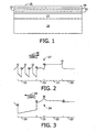
- Fig. 1 illustrates a common III-nitride light-emitting device.
- An n-type region 11 is grown over a sapphire substrate 10.
- the internal quantum efficiency of the device defined as the ratio of the flux of photons generated to the flux of carriers supplied, initially increases, then decreases, as illustrated in Fig. 14 .
- the decrease in internal quantum efficiency at high current density may be at least partially caused by electron leakage from the active region due to the design of the device of Fig. 1 . Also, electron leakage limits the peak efficiency of the device.
- Electron leakage is exacerbated by naturally occurring polarization in wurtzite crystals.
- the crystal layers in III-nitride devices grown on lattice-mismatched substrates such as sapphire are often grown as strained wurtzite crystals.
- Such crystals exhibit two types of polarization: spontaneous polarization, which arises from the crystal symmetry, and piezoelectric polarization, which arises from strain.
- the total polarization in a layer is the sum of the spontaneous and piezoelectric polarization.
- a polarization-induced sheet charge occurs at the interface between layers of different composition. In general, the density of a sheet charge will depend upon both the spontaneous polarization and the piezoelectric polarization due to strain between the two adjacent layers.
- Fig. 2 illustrates a portion of the conduction band of the device of Fig. 1 . The sign and location of the sheet charges are indicated by "+" and "-" signs in Fig. 2 .
- GaN spacer layer 13 may be omitted, other materials may form the barrier, and that the problem with a positive sheet charge at the interface forming the barrier may be generalized to other devices.
- the positive sheet charge at the interface reduces the effective height of the AlGaN barrier, permitting electrons to leak from the active region. Any leakage current recombines nonradiatively in the p-type layers and does not contribute to light emission from the device. As the current density increases, the amount of leakage current increases, contributing to the decrease in internal quantum efficiency at high current density. Also, leakage current is present even at low current densities, reducing the overall peak efficiency of the device.
- the direction of current flow (i.e. the motion of positive charge carriers, or holes) is antiparallel to the direction of the [0001] c-axis.
- This relative arrangement of the current flow and polarization arises from the relative ease of growing Mg-doped p-type III-nitride material after the n-type region rather than before, and the conditions used for conventional growth of high quality III-nitride layers by MOCVD on sapphire substrates, which provide an excess of Ga compared to N present on the crystal surface, resulting in the positive direction of the [0001] c-axis pointing out of the surface of the film. Because the p-type region is placed on top of the n-type region, current will flow from the top of the wafer towards the substrate.
- the light-emitting region of a semiconductor light-emitting device has the reverse-polarization of a conventional III-nitride semiconductor light-emitting device.
- Reverse-polarization refers to reversing the relative arrangement of current flow with respect to the [0001] c-axis, such that the current flow is parallel to the [0001] c-axis, not antiparallel as in the device of Fig. 1 . Reversing the polarization in the light-emitting region may reduce leakage current, potentially increasing the light generating efficiency.
- Fig. 3 illustrates a portion of the conduction band of a device according to embodiments of the invention.
- the barrier on the p-side of the light emitting layer which confines charge carriers in light emitting layer 20, is disposed between spacer layer 21, which may be GaN, and layer 22, which may be p-type Algal.
- spacer layer 21 which may be GaN
- layer 22 which may be p-type Algal.
- the c-axis points toward the light-emitting region, as indicated at 18 in Fig. 3 . In this orientation, the current flow under forward bias operating conditions is parallel to the c-axis.
- light emitting region 20 may be a single thick or thin light emitting layer, as illustrated in Fig. 3 , or may include multiple quantum wells separated by barrier layers, as illustrated in Fig. 2 .
- spacer layer 21 may be doped n-type or not intentionally doped. Since spacer layer 21 is located on the p-side of the light-emitting layer, spacer layer 21 is considered part of the p-type region of the device, even if spacer layer 21 is n-type or undoped.
- Fig. 12 illustrates a unit cell of wurtzite GaN, formed from gallium atoms 93 and nitrogen atoms 94.
- Wurtzite GaN has a gallium face 90 and a nitrogen face 91.
- the c-axis 92 points from the nitrogen face 91 to the gallium face 90.
- the exposed, top surface of GaN created by, for example, conventional growth on a c-plane sapphire substrate, is the gallium face 90.
- Growth on the gallium face 90 of a GaN surface results in the c-axis orientation illustrated in Fig. 2 .
- the buried surface of GaN adjacent to the sapphire after conventional growth on c-plane sapphire is the nitrogen face 91.
- epitaxial structures are grown conventionally such that the gallium face is exposed.
- the epitaxial structure is then bonded to another epitaxial structure or a host substrate and the growth substrate is removed, such that the nitrogen face is exposed.
- the light-emitting region in the resulting device is oriented such that the nitrogen face is the crystal surface facing the p-type region, and an interface between the light emitting region and the p-type region has the c-axis orientation illustrated in Fig. 3 .
- the bond is preferably spaced apart from the light emitting region, such that after processing is complete, a device structure defined as a portion n-type region proximate to one side of the light emitting region, the light emitting region, and a portion of the p-type region proximate the other side of the light emitting region, is uninterrupted by the bond.
- the bond may be spaced at least 500 nm from an edge of the light emitting region.
- the epitaxial surface that is bonded to another epitaxial structure or a host structure may be p-type, n-type, or undoped.
- Fig. 4 illustrates a first method of forming a device with the c-axis orientation of the light-emitting region illustrated in Fig. 3 .
- Two separate epitaxial structures are grown on growth substrates 40 and 46.
- Growth substrates may be any suitable growth substrate, such as, for example, sapphire, SiC, AIN, or GaN.
- An optional n-type, p-type, or undoped region 41, referred to below as an n-type region may be grown over substrate 40.
- a first region 44 which may be n-type, p-type, or undoped, but is referred to below as an n-type region, light emitting region 43, and a second n-type region 42 are grown over substrate 46.
- Light emitting region 43 may be, for example, a single thin or thick light emitting layer, or multiple quantum wells separated by barrier layers.
- N-type region 44 which, after later processing, is located on the p-side of the active region, may include a GaN layer adjacent to light emitting region 43, such as layer 21 of Fig. 3 , and an AIGaN layer adjacent to the GaN layer, such as layer 22 of Fig. 3 .
- Other regions which may be n-type, p-type, or undoped may separate n-type region 44 from substrate 46, and may be formed over n-type region 42 (i.e., between n-type region 42 and the bonded interface with region 41).
- N-type region 44 or any other region between substrate 46 and light emitting region 43 may include release layers designed to facilitate release of the growth substrate by simple chemical etching, or thinning of the epitaxial layers after substrate removal.
- the top surface of the semiconductor structure grown on substrate 46, n-type region 42 in Fig. 4 , and the surface of n-type region 41 are bonded together under elevated temperature and pressure.
- An appropriate temperature for bonding may be, for example, between 500 and 1500 °C; an appropriate pressure for bonding may be, for example, between 5 and 1500 psi.
- the surfaces may be pressed together at the above temperature and pressure in an atmosphere of, for example, N 2 for a specified time period, for example, at least 2 minutes, often for at least 30 minutes. Under these conditions, a robust semiconductor bond is formed between the two surfaces. Such a bond may withstand the temperatures necessary for further semiconductor processing subsequent to bonding, such as growing additional semiconductor layers.
- a diffusion-soldering bond one or more metals such as Zn and Sn are deposited at the bonded interface and bonded at low temperature.
- the ZnSn bond is stable at high temperatures, for example temperatures greater than 900 °C.
- the surfaces are bonded using a thin metallic film such as A1 as a bonding layer. The Al may alloy into the two semiconductor surfaces, creating a bond that is stable at high temperatures.
- one or more dielectric layers such as SiO 2 , Si 3 N 4 , SiON, TiO 2 , SiO 2 , SnO 2 , ZrO 2 , ZnO,MgF 2 , Al 2 O 3 may form one of the bonded surfaces or may be disposed between the two bonded surfaces.
- Bond 50 may be formed between two GaN surfaces, between an InGaN surface and a GaN surface, between two InGaN surfaces, or between any other suitable surfaces.
- the bond may be formed directly between GaN or InGaN and a non-III-nitride host substrate, such as an Al 2 O 3 , Si or SiC substrate.
- substrate 40 and n-type region 41 of Fig. 4 may be replaced by a Si, SiC, or Al 2 O 3 substrate without any epitaxial layers grown on the replacement substrate.
- the host substrate may be a dielectric distributed Bragg reflector. "Wavelength-Converted Semiconductor Light Emitting Device," Application Serial No. [Attorney Docket No.
- LUM-04-02-07 describes a ceramic body, which may be used as a host substrate.
- the host substrate must be able to tolerate the conditions required for any processing to take place after the bond.
- the two bonded surfaces may be optionally smoothed prior to bonding, for example by polishing by conventional methods.
- the two epitaxial structures are grown in conditions that favor formation of smooth surfaces for bonding.
- a sapphire growth substrate may be removed by exposing, through substrate 46, portions of the interface between substrate 46 and crystal region 44 to a high fluence pulsed ultraviolet laser in a step and repeat pattern.
- the exposed portions may be isolated by trenches etched through the crystal layers of the device, in order to isolate the shock wave caused by exposure to the laser. Such etching is done prior to bonding.
- the photon energy of the laser is above the band gap of the crystal layer adjacent to the sapphire (GaN in some embodiments), thus the pulse energy is effectively converted to thermal energy within the first 100 nm of epitaxial material adjacent to the sapphire.
- sufficiently high fluence i.e.
- the temperature within the first 100 nm rises on a nanosecond scale to a temperature greater than 1000°C, high enough for the GaN to dissociate into gallium and nitrogen gasses, releasing the epitaxial layers from substrate 46.
- Other substrates, such as SiC, Si, and engineered substrates based on Si may be removed by conventional processes, such as etching and/or lapping.
- n-type region 44a may be thinned to just above light emitting region 43 by dry etching, wet etching such as photoelectrochemical etching, and/or chemical mechanical polishing.
- p-type region 52 is formed by diffusing a p-type dopant such as Mg into thinned n-type region 44b, thus converting the conductivity of this region from n-type to p-type.
- Mg and Au may be thermally evaporated on the surface of n-type region 44a, then heated, for example to a temperature of 900 °C for six hours. The remaining Mg and Au are then removed by etching, and the device annealed, for example at a temperature between 850 and 1050 °C, to activate the diffused Mg.
- a p-type dopant such as Mg (often co-implanted with P) or Be (often co-implanted with O) may be implanted into n-type region 44b.
- a Ni layer may be formed on n-type region 44b to protect the surface during implant, then Be metal and O 2 gas are used to implant Be and O into n-type region 44b at an energy greater than 50keV and a dosage between 10 13 cm -2 and 10 16 cm -2 .
- the Ni is then removed and the device is annealed at a temperature greater than 900 °C to activate the implanted dopant.
- Implantation may also be used to increase the doping level of an already p-type material, for example p-type region 52 described below in reference to Fig. 7 .
- p-type region 52 is grown over thinned n-type region 44a.
- P-type region 52 may be grown in conventional growth conditions, after an optional cleaning of the surface by, for example, etching. Regrowth of p-type region 52 is possible because every structure in the device, including semiconductor bond 50, can withstand the high temperatures required for III-nitride growth.
- n-type region 44 exposed by removal of substrate 46 is the nitrogen face. Accordingly, p-type region 52, whether formed by diffusion or implantation of a p-type dopant into an n-type region or by growth on the exposed n-type region, will also have the nitrogen face up, resulting in the desirable c-axis orientation between the active region and the p-type region illustrated in Fig. 3 .
- Nitrogen-face films may be grown by, for example, molecular beam epitaxy or MOCVD, as described in more detail in " Morphological and structure characteristics of homoepitaxial GaN grown by metalorganic chemical vapour deposition (MOCVD)," Journal of Crystal Growth 204 (1999) 419-428 and " Playing with Polarity", Phys. Stat. Sol. (b) 228, No. 2, 505-512 (2001 ).
- Figs. 6 and 7 are now ready for conventional flip chip processing, which requires etching a mesa to expose a portion of one of n-type regions 42 or 41, forming transparent or reflective contacts on n-type region 42 or 41 and p-type region 52, and mounting the device such that light is extracted either through the contacts (in the case of transparent contacts) or through substrate 40 (in the case of reflective contacts).
- the device may processed as a thin film device, wherein the surface of p-type region 52 in either of Figs.
- 6 and 7 may be metal-bonded to a host substrate through a bond that forms a contact to p-type region 52, then substrate 40 may be removed, a contact may be formed on the exposed surface of n-type region 41, and the device may be mounted such that light is extracted through the exposed surface of n-type region 41.
- the host substrate is a dielectric distributed Bragg reflector
- a vertical cavity laser or a resonant cavity light emitting diode may be formed.
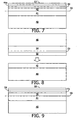
- Fig. 8 illustrates a second method of forming a device according to Fig. 3 .
- two separate epitaxial structures are grown on growth substrates 40 and 46.
- n-type, p-type, or undoped region 41 referred to below as an n-type region, is grown over substrate. 40.
- p-type region 54 is grown first, followed by light emitting region 53 and n-type region 56.
- P-type region 54 may include a GaN layer adjacent to light emitting region 53, such as layer 21 of Fig. 3 , and an AlGaN layer adjacent to the GaN layer, such as layer 22 of Fig. 3 .
- regions which may be n-type, p-type, or undoped may separate p-type region 54 from substrate 46, and may be formed over n-type region 56 (i.e., between n-type region 56 and the bonded interface with region 41).
- n-type region 41 may be omitted and n-type region 56 may be directly bonded to a suitable host structure.
- Substrate 46 is then removed, as described above, and p-type region 54 may optionally be thinned.
- P-type region 54 may include release layers designed to facilitate release of the growth substrate by simple chemical etching, or thinning of the epitaxial layers after substrate removal.
- a second p-type region 58 may be grown on the surface of p-type region 54 after the removal of substrate 46, or a p-type dopant such as Mg may be diffused or implanted into p-type region 54, as illustrated in Fig. 9 .
- growth of a second p-type region, diffusion, or implantation are necessary after thinning to recover from crystalline damage that occurs during thinning. Growth of a p-type region 58 after thinning may be desirable to space the damage caused by thinning apart from light emitting layer 53, since such damage may cause optical and electrical losses. Damage to the surface of p-type region 54 may be repaired by a high temperature anneal in NH 3 .
- the device may be annealed at a pressure of 200 Torr and a temperature of 850 to 1000 °C.
- a p-type dopant precursor such as CP 2 Mg may be added during the anneal to repair p-type region 54, or to further dope p-type region 54 to reduce contact resistance.
- the device illustrated in Fig. 9 may then be processed as a flip chip or thin film device, as described above.
- one surface is roughened or textured prior to bonding.
- Figs. 10 and 11 illustrate embodiments that include a textured region 60.
- textured region 60 is a photonic crystal region in the form of a periodic array of holes. Photonic crystal structures are described in more detail in U.S. Pub. No. 2003/0141507 titled "LED efficiency using photonic crystal structure".
- the periodic array of holes has a lattice constant a, which may range from 0.1 ⁇ to 4 ⁇ , where ⁇ is the wavelength of light emitting by the active region within the semiconductor structure. In other embodiments, features larger than 2 microns are formed in textured region 60. Textured region 60 is bonded to 41 by a bond 50 as illustrated in Fig. z10.
- the structure may then be flipped over and bonded to a host substrate 65 by a bond such as a metal bond (not shown) formed at the interface between p-type region 58 and host substrate 65, as illustrated in Fig. 11 .
- Substrate 40 of Fig. 10 is then removed, and a contact (not shown) may be formed on the exposed surface of region 41, through which light is extracted from the device.
- Textured region 60 acts as a buried light scattering layer within the device, which may increase the amount of light extracted from the device.
- Fig. 11 illustrates a thin film device
- the bonded device of Fig. 10 may also be processed into a flip chip device as described above.
- Figs. 10 and 11 show a device similar to that shown in Figs.
- a textured or roughened region is formed over n-type region 56, such a textured or roughened region may be incorporated into a device as illustrated in Figs. 4, 5, 6 , and 7 , where the textured or roughened region is formed over n-type region 42, then bonded to region 41.
- Fig. 13 is an exploded view of a packaged light-emitting device, as described in more detail in U.S. Patent 6,274,924 .
- a heat-sinking slug 100 is placed into an insert-molded leadframe.
- the insert-molded leadframe is, for example, a filled plastic material 105 molded around a metal frame 106 that provides an electrical path.
- Slug 100 may include an optional reflector cup 102.
- the light emitting device die 104 which may be any of the devices described above, is mounted directly or indirectly via a thermally conducting submount 103 to slug 100.
- a cover 108 which may be an optical lens, may be added.
- III-nitride lasers are limited to a wavelength range from near UV (390nm) to blue (460nm). Lowering the current threshold where stimulated emission begins may expand the potential operating wavelength of III-nitride lasers into UV and toward green.
- the current leakage also limits the total output power of the lasers, so by reducing this leakage, embodiments of the present invention may enable higher power III-nitride lasers.
- the light-emitting device structure may be grown on low dislocation templates for increased reliability.
- FIG. 15 An edge-emitting laser is illustrated in Fig 15 .
- the device of Fig. 15 contains the same epitaxial layers as Fig 9 , though a laser may also be formed with the same epitaxial layers as Figs. 6 or 7 .
- a stripe mesa structure is etched to n-type region 56 layer to define the laser cavity width and to reveal n-type region 56 for contacting.
- N-contact 57 and p-contact 55 are deposited and defined with standard techniques.
- the cavity is defined length-wise (out of the page) by dry etching or cleaving the laser facets.
- An additional AIGaN cladding layer may be added between regions 53 and 56 to confine the optical laser mode in the vertical direction.
Landscapes
- Physics & Mathematics (AREA)
- Condensed Matter Physics & Semiconductors (AREA)
- General Physics & Mathematics (AREA)
- Electromagnetism (AREA)
- Optics & Photonics (AREA)
- Led Devices (AREA)
- Polarising Elements (AREA)
- Electroluminescent Light Sources (AREA)
Abstract
Description
- This invention relates to a semiconductor light-emitting device with a polarization-reversed light emitting region, and methods of making such a device.
- Semiconductor light-emitting devices including light emitting diodes (LEDs), resonant cavity light emitting diodes (RCLEDs), vertical cavity laser diodes (VCSELs), and edge emitting lasers are among the most efficient light sources currently available. Materials systems currently of interest in the manufacture of high-brightness light emitting devices capable of operation across the visible spectrum include Group III-V semiconductors, particularly binary, ternary, and quaternary alloys of gallium, aluminum, indium, and nitrogen, also referred to as III-nitride materials. Typically, m-nitride light emitting devices are fabricated by epitaxially growing a stack of semiconductor layers of different compositions and dopant concentrations on a sapphire, silicon carbide, III-nitride, or other suitable substrate by metal-organic chemical vapor deposition (MOCVD), molecular beam epitaxy (MBE), or other epitaxial techniques. The stack often includes one or more n-type layers doped with, for example, Si, formed over the substrate, a light emitting or active region formed over the n-type layer or layers, and one or more p-type layers doped with, for example, Mg, formed over the active region. III-nitride devices formed on conductive substrates may have the p- and n-contacts formed on opposite sides of the device. Often, III-nitride devices are fabricated on insulating substrates, such as sapphire, with both contacts on the same side of the device. Such devices are mounted so light is extracted either through the contacts (known as an epitaxy-up device) or through a surface of the device opposite the contacts (known as a flip chip device).
Needed in the art is III-nitride light emitting devices that operate efficiently at high current density. -
US-A-2002/0110172 discloses for example a light emitter having a reversed polarisation field in respect to the whole pn-junction. - The object of the present invention is fulfilled by a device and a method as defined in
claims 1 and 13, respectively. Preferred embodiments are defined in the dependent claims. -
-
Fig. 1 illustrates an III-nitride light-emitting device. -
Fig. 2 illustrates a portion of the conduction band for the device ofFig. 1 . -
Fig. 3 illustrates a portion of the conduction band for a device according to embodiments of the invention. -
Fig. 4 illustrates bonding two epitaxial structures together. -
Fig. 5 illustrates the device ofFig. 4 after removal of one growth substrate and optional thinning of the exposed epitaxial layer. -
Fig. 6 illustrates the device ofFig. 5 after diffusion or implantation ofp-type dopant. -
Fig. 7 illustrates the device ofFig. 5 after regrowth of a new p-type region. -
Fig. 8 illustrates bonding two epitaxial structures together. -
Fig. 9 illustrates the device ofFig. 8 after removal of one growth substrate and optional regrowth of a new p-type region. -
Fig. 10 illustrates a device incorporating a textured region. -
Fig. 11 illustrates the device ofFig. 10 after bonding to a host substrate removal of the second growth substrate. -
Fig. 12 illustrates a unit cell of wurtzite GaN. -
Fig. 13 is an exploded view of a packaged light-emitting device. -
Fig. 14 is a plot of quantum efficiency as a function of current density. -
Fig. 15 illustrates a laser according to embodiments of the invention. -
Fig. 1 illustrates a common III-nitride light-emitting device. An n-type region 11 is grown over asapphire substrate 10. Anactive region 12, which may include multiple quantum wells separated by barrier layers, is grown over n-type region 11, followed by aGaN spacer layer 13, a p-type AlGaN layer 14, and a p-type contact layer 15. - As the current density applied to the device of
Fig. 1 increases, the internal quantum efficiency of the device, defined as the ratio of the flux of photons generated to the flux of carriers supplied, initially increases, then decreases, as illustrated inFig. 14 . The decrease in internal quantum efficiency at high current density may be at least partially caused by electron leakage from the active region due to the design of the device ofFig. 1 . Also, electron leakage limits the peak efficiency of the device. - Electron leakage is exacerbated by naturally occurring polarization in wurtzite crystals. The crystal layers in III-nitride devices grown on lattice-mismatched substrates such as sapphire are often grown as strained wurtzite crystals. Such crystals exhibit two types of polarization: spontaneous polarization, which arises from the crystal symmetry, and piezoelectric polarization, which arises from strain. The total polarization in a layer is the sum of the spontaneous and piezoelectric polarization. A polarization-induced sheet charge occurs at the interface between layers of different composition. In general, the density of a sheet charge will depend upon both the spontaneous polarization and the piezoelectric polarization due to strain between the two adjacent layers.
Fig. 2 illustrates a portion of the conduction band of the device ofFig. 1 . The sign and location of the sheet charges are indicated by "+" and "-" signs inFig. 2 . - Conventional growth on a typical substrate, such as sapphire or SiC, results in the wurtzite c-axis orientation indicated at 18 in
Fig. 2 . Across the interface between the active region and the p-type layers, the c-axis points toward the p-type layers. This orientation results in a positive sheet charge at the interface betweenGaN spacer layer 13 and p-type AlGaN layer 14. In the device illustrated inFig. 1 , theinterface 17 betweenGaN spacer layer 13 and p-type AlGaN layer 14 is intended to form a "barrier" to confine conduction band electrons in the active region. It is to be understood that GaNspacer layer 13 may be omitted, other materials may form the barrier, and that the problem with a positive sheet charge at the interface forming the barrier may be generalized to other devices. The positive sheet charge at the interface reduces the effective height of the AlGaN barrier, permitting electrons to leak from the active region. Any leakage current recombines nonradiatively in the p-type layers and does not contribute to light emission from the device. As the current density increases, the amount of leakage current increases, contributing to the decrease in internal quantum efficiency at high current density. Also, leakage current is present even at low current densities, reducing the overall peak efficiency of the device. - In the III-nitride device illustrated in
Fig. 1 , the direction of current flow (i.e. the motion of positive charge carriers, or holes) is antiparallel to the direction of the [0001] c-axis. This relative arrangement of the current flow and polarization arises from the relative ease of growing Mg-doped p-type III-nitride material after the n-type region rather than before, and the conditions used for conventional growth of high quality III-nitride layers by MOCVD on sapphire substrates, which provide an excess of Ga compared to N present on the crystal surface, resulting in the positive direction of the [0001] c-axis pointing out of the surface of the film. Because the p-type region is placed on top of the n-type region, current will flow from the top of the wafer towards the substrate. - In accordance with embodiments of the invention, the light-emitting region of a semiconductor light-emitting device has the reverse-polarization of a conventional III-nitride semiconductor light-emitting device. "Reverse-polarization" refers to reversing the relative arrangement of current flow with respect to the [0001] c-axis, such that the current flow is parallel to the [0001] c-axis, not antiparallel as in the device of
Fig. 1 . Reversing the polarization in the light-emitting region may reduce leakage current, potentially increasing the light generating efficiency. -
Fig. 3 illustrates a portion of the conduction band of a device according to embodiments of the invention. In the device illustrated inFig. 3 , the barrier on the p-side of the light emitting layer, which confines charge carriers inlight emitting layer 20, is disposed betweenspacer layer 21, which may be GaN, andlayer 22, which may be p-type Algal. Across the interface between the light emitting region and the p-type region, betweenlayers Fig. 3 . In this orientation, the current flow under forward bias operating conditions is parallel to the c-axis. This orientation results in a negative sheet charge at the barrier 24 (the interface betweenlayers 21 and 22), which increases the barrier height, reducing the electron current that leaks pastlight emitting region 20. In embodiments of the invention,light emitting region 20 may be a single thick or thin light emitting layer, as illustrated inFig. 3 , or may include multiple quantum wells separated by barrier layers, as illustrated inFig. 2 . In some embodiments,spacer layer 21. may be doped n-type or not intentionally doped. Sincespacer layer 21 is located on the p-side of the light-emitting layer,spacer layer 21 is considered part of the p-type region of the device, even ifspacer layer 21 is n-type or undoped. -
Fig. 12 illustrates a unit cell of wurtzite GaN, formed fromgallium atoms 93 andnitrogen atoms 94. Wurtzite GaN has agallium face 90 and anitrogen face 91. The c-axis 92 points from thenitrogen face 91 to thegallium face 90. The exposed, top surface of GaN created by, for example, conventional growth on a c-plane sapphire substrate, is thegallium face 90. Growth on thegallium face 90 of a GaN surface results in the c-axis orientation illustrated inFig. 2 . The buried surface of GaN adjacent to the sapphire after conventional growth on c-plane sapphire is thenitrogen face 91. In embodiments of the invention, epitaxial structures are grown conventionally such that the gallium face is exposed. The epitaxial structure is then bonded to another epitaxial structure or a host substrate and the growth substrate is removed, such that the nitrogen face is exposed. As a result of growth or processing after bonding, the light-emitting region in the resulting device is oriented such that the nitrogen face is the crystal surface facing the p-type region, and an interface between the light emitting region and the p-type region has the c-axis orientation illustrated inFig. 3 . - The bond is preferably spaced apart from the light emitting region, such that after processing is complete, a device structure defined as a portion n-type region proximate to one side of the light emitting region, the light emitting region, and a portion of the p-type region proximate the other side of the light emitting region, is uninterrupted by the bond. For example, in some embodiments the bond may be spaced at least 500 nm from an edge of the light emitting region. The epitaxial surface that is bonded to another epitaxial structure or a host structure may be p-type, n-type, or undoped.
-
Fig. 4 illustrates a first method of forming a device with the c-axis orientation of the light-emitting region illustrated inFig. 3 . Two separate epitaxial structures are grown ongrowth substrates undoped region 41, referred to below as an n-type region, may be grown oversubstrate 40. Afirst region 44, which may be n-type, p-type, or undoped, but is referred to below as an n-type region, light emittingregion 43, and a second n-type region 42 are grown oversubstrate 46.Light emitting region 43 may be, for example, a single thin or thick light emitting layer, or multiple quantum wells separated by barrier layers. N-type region 44, which, after later processing, is located on the p-side of the active region, may include a GaN layer adjacent to light emittingregion 43, such aslayer 21 ofFig. 3 , and an AIGaN layer adjacent to the GaN layer, such aslayer 22 ofFig. 3 . Other regions which may be n-type, p-type, or undoped may separate n-type region 44 fromsubstrate 46, and may be formed over n-type region 42 (i.e., between n-type region 42 and the bonded interface with region 41). N-type region 44 or any other region betweensubstrate 46 andlight emitting region 43 may include release layers designed to facilitate release of the growth substrate by simple chemical etching, or thinning of the epitaxial layers after substrate removal. - The top surface of the semiconductor structure grown on
substrate 46, n-type region 42 inFig. 4 , and the surface of n-type region 41 are bonded together under elevated temperature and pressure. An appropriate temperature for bonding may be, for example, between 500 and 1500 °C; an appropriate pressure for bonding may be, for example, between 5 and 1500 psi. The surfaces may be pressed together at the above temperature and pressure in an atmosphere of, for example, N2 for a specified time period, for example, at least 2 minutes, often for at least 30 minutes. Under these conditions, a robust semiconductor bond is formed between the two surfaces. Such a bond may withstand the temperatures necessary for further semiconductor processing subsequent to bonding, such as growing additional semiconductor layers. Other bonding techniques besides semiconductor wafer bonding may be used, such as diffusion soldering bonding. In a diffusion-soldering bond, one or more metals such as Zn and Sn are deposited at the bonded interface and bonded at low temperature. The ZnSn bond is stable at high temperatures, for example temperatures greater than 900 °C. In another alternative method, the surfaces are bonded using a thin metallic film such as A1 as a bonding layer. The Al may alloy into the two semiconductor surfaces, creating a bond that is stable at high temperatures. In some embodiments, one or more dielectric layers such as SiO2, Si3N4, SiON, TiO2, SiO2, SnO2, ZrO2, ZnO,MgF2, Al2O3 may form one of the bonded surfaces or may be disposed between the two bonded surfaces. - Bond 50 (
Fig. 5 ) may be formed between two GaN surfaces, between an InGaN surface and a GaN surface, between two InGaN surfaces, or between any other suitable surfaces. Alternatively, the bond may be formed directly between GaN or InGaN and a non-III-nitride host substrate, such as an Al2O3, Si or SiC substrate. For example,substrate 40 and n-type region 41 ofFig. 4 may be replaced by a Si, SiC, or Al2O3 substrate without any epitaxial layers grown on the replacement substrate. Alternatively, the host substrate may be a dielectric distributed Bragg reflector. "Wavelength-Converted Semiconductor Light Emitting Device," Application Serial No. [Attorney Docket No. LUM-04-02-07], describes a ceramic body, which may be used as a host substrate. In some embodiments, the host substrate must be able to tolerate the conditions required for any processing to take place after the bond. The two bonded surfaces may be optionally smoothed prior to bonding, for example by polishing by conventional methods. In some embodiments, the two epitaxial structures are grown in conditions that favor formation of smooth surfaces for bonding. - After bonding,
substrate 46 from the top device is removed, as illustrated inFig. 5 . A sapphire growth substrate may be removed by exposing, throughsubstrate 46, portions of the interface betweensubstrate 46 andcrystal region 44 to a high fluence pulsed ultraviolet laser in a step and repeat pattern. The exposed portions may be isolated by trenches etched through the crystal layers of the device, in order to isolate the shock wave caused by exposure to the laser. Such etching is done prior to bonding. The photon energy of the laser is above the band gap of the crystal layer adjacent to the sapphire (GaN in some embodiments), thus the pulse energy is effectively converted to thermal energy within the first 100 nm of epitaxial material adjacent to the sapphire. At sufficiently high fluence (i.e. greater than about 500 mJ/cm2) and a photon energy above the band gap of GaN and below the absorption edge of sapphire (i.e. between about 3.44 and about 6 eV), the temperature within the first 100 nm rises on a nanosecond scale to a temperature greater than 1000°C, high enough for the GaN to dissociate into gallium and nitrogen gasses, releasing the epitaxial layers fromsubstrate 46. Other substrates, such as SiC, Si, and engineered substrates based on Si may be removed by conventional processes, such as etching and/or lapping. - After removal of
substrate 46, the resulting structure in the example ofFig. 5 includes epitaxial n-type region 44,active region 43, and n-type region 42 bonded throughbond 50 to n-type region 41 andsubstrate 40. Aftersubstrate 46 is removed, n-type region 44a (Fig. 5 ) may be thinned to just abovelight emitting region 43 by dry etching, wet etching such as photoelectrochemical etching, and/or chemical mechanical polishing. - A p-type region is then formed over light emitting
region 43. InFig. 6 , p-type region 52 is formed by diffusing a p-type dopant such as Mg into thinned n-type region 44b, thus converting the conductivity of this region from n-type to p-type. For example, Mg and Au may be thermally evaporated on the surface of n-type region 44a, then heated, for example to a temperature of 900 °C for six hours. The remaining Mg and Au are then removed by etching, and the device annealed, for example at a temperature between 850 and 1050 °C, to activate the diffused Mg. Alternatively, a p-type dopant such as Mg (often co-implanted with P) or Be (often co-implanted with O) may be implanted into n-type region 44b. For example, a Ni layer may be formed on n-type region 44b to protect the surface during implant, then Be metal and O2 gas are used to implant Be and O into n-type region 44b at an energy greater than 50keV and a dosage between 1013 cm-2 and 1016 cm-2. The Ni is then removed and the device is annealed at a temperature greater than 900 °C to activate the implanted dopant. Implantation may also be used to increase the doping level of an already p-type material, for example p-type region 52 described below in reference toFig. 7 . - In
Fig. 7 , p-type region 52 is grown over thinned n-type region 44a. P-type region 52 may be grown in conventional growth conditions, after an optional cleaning of the surface by, for example, etching. Regrowth of p-type region 52 is possible because every structure in the device, includingsemiconductor bond 50, can withstand the high temperatures required for III-nitride growth. - The surface of n-
type region 44 exposed by removal ofsubstrate 46 is the nitrogen face. Accordingly, p-type region 52, whether formed by diffusion or implantation of a p-type dopant into an n-type region or by growth on the exposed n-type region, will also have the nitrogen face up, resulting in the desirable c-axis orientation between the active region and the p-type region illustrated inFig. 3 . Nitrogen-face films may be grown by, for example, molecular beam epitaxy or MOCVD, as described in more detail in "Morphological and structure characteristics of homoepitaxial GaN grown by metalorganic chemical vapour deposition (MOCVD)," Journal of Crystal Growth 204 (1999) 419-428 and "Playing with Polarity", Phys. Stat. Sol. (b) 228, No. 2, 505-512 (2001). - The devices illustrated in
Figs. 6 and7 are now ready for conventional flip chip processing, which requires etching a mesa to expose a portion of one of n-type regions type region type region 52, and mounting the device such that light is extracted either through the contacts (in the case of transparent contacts) or through substrate 40 (in the case of reflective contacts). Alternatively, the device may processed as a thin film device, wherein the surface of p-type region 52 in either ofFigs. 6 and7 may be metal-bonded to a host substrate through a bond that forms a contact to p-type region 52, thensubstrate 40 may be removed, a contact may be formed on the exposed surface of n-type region 41, and the device may be mounted such that light is extracted through the exposed surface of n-type region 41. In embodiments where the host substrate is a dielectric distributed Bragg reflector, a vertical cavity laser or a resonant cavity light emitting diode may be formed. -
Fig. 8 illustrates a second method of forming a device according toFig. 3 . As inFig. 4 , two separate epitaxial structures are grown ongrowth substrates Fig 4 , n-type, p-type, orundoped region 41, referred to below as an n-type region, is grown over substrate. 40. Oversubstrate 46, p-type region 54 is grown first, followed by light emittingregion 53 and n-type region 56. P-type region 54 may include a GaN layer adjacent to light emittingregion 53, such aslayer 21 ofFig. 3 , and an AlGaN layer adjacent to the GaN layer, such aslayer 22 ofFig. 3 . Other regions which may be n-type, p-type, or undoped may separate p-type region 54 fromsubstrate 46, and may be formed over n-type region 56 (i.e., between n-type region 56 and the bonded interface with region 41). - The top surface of the semiconductor structure grown on
substrate 46, n-type region 56 inFig. 8 , and the surface of n-type region 41 are bonded together under similar conditions as those described in reference toFig. 4 . As described above, n-type region 41 may be omitted and n-type region 56 may be directly bonded to a suitable host structure.Substrate 46 is then removed, as described above, and p-type region 54 may optionally be thinned. P-type region 54 may include release layers designed to facilitate release of the growth substrate by simple chemical etching, or thinning of the epitaxial layers after substrate removal. A second p-type region 58 may be grown on the surface of p-type region 54 after the removal ofsubstrate 46, or a p-type dopant such as Mg may be diffused or implanted into p-type region 54, as illustrated inFig. 9 . In some embodiments, growth of a second p-type region, diffusion, or implantation are necessary after thinning to recover from crystalline damage that occurs during thinning. Growth of a p-type region 58 after thinning may be desirable to space the damage caused by thinning apart from light emittinglayer 53, since such damage may cause optical and electrical losses. Damage to the surface of p-type region 54 may be repaired by a high temperature anneal in NH3. For example, the device may be annealed at a pressure of 200 Torr and a temperature of 850 to 1000 °C. A p-type dopant precursor such as CP2Mg may be added during the anneal to repair p-type region 54, or to further dope p-type region 54 to reduce contact resistance. The device illustrated inFig. 9 may then be processed as a flip chip or thin film device, as described above. - In some embodiments, one surface is roughened or textured prior to bonding.
Figs. 10 and 11 illustrate embodiments that include atextured region 60. In some embodiments,textured region 60 is a photonic crystal region in the form of a periodic array of holes. Photonic crystal structures are described in more detail inU.S. Pub. No. 2003/0141507 titled "LED efficiency using photonic crystal structure". The periodic array of holes has a lattice constant a, which may range from 0.1λ to 4λ, where λ is the wavelength of light emitting by the active region within the semiconductor structure. In other embodiments, features larger than 2 microns are formed intextured region 60.Textured region 60 is bonded to 41 by abond 50 as illustrated in Fig. z10. The structure may then be flipped over and bonded to ahost substrate 65 by a bond such as a metal bond (not shown) formed at the interface between p-type region 58 andhost substrate 65, as illustrated inFig. 11 .Substrate 40 ofFig. 10 is then removed, and a contact (not shown) may be formed on the exposed surface ofregion 41, through which light is extracted from the device.Textured region 60 acts as a buried light scattering layer within the device, which may increase the amount of light extracted from the device. ThoughFig. 11 illustrates a thin film device, the bonded device ofFig. 10 may also be processed into a flip chip device as described above. Also, thoughFigs. 10 and 11 show a device similar to that shown inFigs. 8 and 9 , where the p-type region 54 is grown prior to thelight emitting region 53, then the textured or roughened region is formed over n-type region 56, such a textured or roughened region may be incorporated into a device as illustrated inFigs. 4, 5, 6 , and7 , where the textured or roughened region is formed over n-type region 42, then bonded toregion 41. -
Fig. 13 is an exploded view of a packaged light-emitting device, as described in more detail inU.S. Patent 6,274,924 . A heat-sinking slug 100 is placed into an insert-molded leadframe. The insert-molded leadframe is, for example, a filledplastic material 105 molded around ametal frame 106 that provides an electrical path.Slug 100 may include anoptional reflector cup 102. The light emitting device die 104, which may be any of the devices described above, is mounted directly or indirectly via a thermally conductingsubmount 103 to slug 100. Acover 108, which may be an optical lens, may be added. The devices illustrated inFigs. 7, 9 and10 may be processed into edge-emitting or vertical-cavity surface emitting lasers. Reduced carrier leakage provided by these structures may improve the laser operating characteristics, such as the threshold current. The threshold current can be written as:
- An edge-emitting laser is illustrated in
Fig 15 . The device ofFig. 15 contains the same epitaxial layers asFig 9 , though a laser may also be formed with the same epitaxial layers asFigs. 6 or7 . A stripe mesa structure is etched to n-type region 56 layer to define the laser cavity width and to reveal n-type region 56 for contacting. N-contact 57 and p-contact 55 are deposited and defined with standard techniques. The cavity is defined length-wise (out of the page) by dry etching or cleaving the laser facets. An additional AIGaN cladding layer may be added betweenregions
Claims (20)
- A structure comprising- a device structure comprising a III-nitride light emitting region (43, 53) disposed between a p-type region (52, 58) and an n-type region (42, 56), the light emitting region comprising a wurtzite crystal structure,
wherein across an interface between the light emitting region and the p-type region a wurtzite c-axis (92), defined as pointing from a nitrogen face (91) of a III-nitride unit cell to a gallium face (90) of a III-nitride unit cell, points toward the light emitting region, and- a bond (50) connecting a surface of the n-region and a surface of a host structure (40, 41),CHARACTERIZED IN THAT
the p-region comprises a barrier (24) having a negative sheet charge being adapted to reduce, in operation, electron current leakage from the light emitting region. - The structure of claim 1, wherein one of the two surfaces is selected from the group GaN, AlN, InGaN, SiC, and Si.
- The structure of claim 1, wherein one of the two surfaces comprises a dielectric layer.
- The structure of claim 3, wherein the dielectric layer is selected from the group SiO2, Si3N4, SiON, TiO2, SiO2, SnO2, ZrO2, ZnO,MgF2, and Al2O3.
- The structure of claim 1, wherein one of the two surfaces is textured.
- The structure of claim 5, wherein the textured surface comprises a periodic array of holes formed in the textured surface.
- The structure of claim 6, wherein the periodic array of holes has a lattice constant between 0.1λ and 4λ, wherein λ is a wavelength of light in the light emitting region.
- The structure of claim 1, wherein the bond (50) comprises a semiconductor bond and is substantially free of metal.
- The structure of claim 1, wherein the bond (50) comprises a metal layer.
- The structure of claim 1, wherein the bond (50) comprises a metal - semiconductor alloy.
- The structure of claim 1, further comprising contacts electrically connected to the n-type region (42, 56) and the p-type region (52, 58).
- The structure of claim 1, further comprising: a mesa including a portion of the light emitting region (43, 53); and laser facets disposed on opposite ends of the mesa.
- A method of forming a semiconductor light emitting device, the method comprising- providing an epitaxial structure comprising a III-nitride region (44, 54) grown on a growth substrate (46), a light emitting region (43, 53) grown over the III-nitride region, and an n-type region (42, 56) grown over the light emitting region,- bonding the epitaxial structure to a host structure by a bond (50) between a surface of the epitaxial structure and a surface of the host structure, wherein at least one of the surfaces is a III-nitride surface,- removing the growth substrate (46) to expose a nitrogen-face (91) of a wurtzite III-nitride unit cell of the epitaxial structure,- after removing the growth substrate (46), forming a p-type region (52, 58) on or in the epitaxial structure, the p-type region comprising a barrier (24) having a negative sheet charge being adapted to reduce, in operation, electron current leakage from the light emitting region.
- The method of claim 13, wherein bonding comprises bonding the host structure to the epitaxial structure such that the n-type region is disposed between the light emitting region and the bond.
- The method of claim 14, further comprising thinning the III-nitride region (44, 54) after removing the growth substrate (46) to form a remaining portion of the III-nitride region.
- The method of claim 15, further comprising diffusing or implanting a p-type dopant into the remaining portion of the III-nitride region (44, 54).
- The method of claim 16, further comprising annealing the remaining portion after diffusing or implanting.
- The method of claim 15, further comprising growing the p-type region (52, 58) over the remaining portion of the III-nitride region (44, 54).
- The method of claim 13, wherein the host structure comprises a distributed Bragg reflector.
- The method of claim 13, further comprising:- forming a mesa including a portion of the light emitting region (43, 53); and- forming laser facets on opposite ends of the mesa.
Applications Claiming Priority (2)
| Application Number | Priority Date | Filing Date | Title |
|---|---|---|---|
| US11/080,022 US7804100B2 (en) | 2005-03-14 | 2005-03-14 | Polarization-reversed III-nitride light emitting device |
| PCT/IB2006/050756 WO2006097878A1 (en) | 2005-03-14 | 2006-03-10 | Polarization-reversed iii-nitride light-emitting device |
Publications (2)
| Publication Number | Publication Date |
|---|---|
| EP1861905A1 EP1861905A1 (en) | 2007-12-05 |
| EP1861905B1 true EP1861905B1 (en) | 2009-01-14 |
Family
ID=36637000
Family Applications (1)
| Application Number | Title | Priority Date | Filing Date |
|---|---|---|---|
| EP06727657A Expired - Lifetime EP1861905B1 (en) | 2005-03-14 | 2006-03-10 | Polarization-reversed iii-nitride light-emitting device |
Country Status (9)
| Country | Link |
|---|---|
| US (1) | US7804100B2 (en) |
| EP (1) | EP1861905B1 (en) |
| JP (1) | JP5174327B2 (en) |
| KR (1) | KR101256378B1 (en) |
| CN (1) | CN101164209B (en) |
| AT (1) | ATE421176T1 (en) |
| DE (1) | DE602006004855D1 (en) |
| TW (1) | TWI420687B (en) |
| WO (1) | WO2006097878A1 (en) |
Families Citing this family (28)
| Publication number | Priority date | Publication date | Assignee | Title |
|---|---|---|---|---|
| US10374120B2 (en) * | 2005-02-18 | 2019-08-06 | Koninklijke Philips N.V. | High efficiency solar cells utilizing wafer bonding and layer transfer to integrate non-lattice matched materials |
| TW200707799A (en) | 2005-04-21 | 2007-02-16 | Aonex Technologies Inc | Bonded intermediate substrate and method of making same |
| JP2007165478A (en) * | 2005-12-12 | 2007-06-28 | National Univ Corp Shizuoka Univ | Photocathode and photodetector |
| US20070243703A1 (en) * | 2006-04-14 | 2007-10-18 | Aonex Technololgies, Inc. | Processes and structures for epitaxial growth on laminate substrates |
| US8193020B2 (en) * | 2006-11-15 | 2012-06-05 | The Regents Of The University Of California | Method for heteroepitaxial growth of high-quality N-face GaN, InN, and AlN and their alloys by metal organic chemical vapor deposition |
| CA2669228C (en) * | 2006-11-15 | 2014-12-16 | The Regents Of The University Of California | Method for heteroepitaxial growth of high-quality n-face gan, inn, and ain and their alloys by metal organic chemical vapor deposition |
| US20080111144A1 (en) * | 2006-11-15 | 2008-05-15 | The Regents Of The University Of California | LIGHT EMITTING DIODE AND LASER DIODE USING N-FACE GaN, InN, AND AlN AND THEIR ALLOYS |
| WO2008060531A2 (en) * | 2006-11-15 | 2008-05-22 | The Regents Of The University Of California | Light emitting diode and laser diode using n-face gan, inn, and ain and their alloys |
| US20080149946A1 (en) | 2006-12-22 | 2008-06-26 | Philips Lumileds Lighting Company, Llc | Semiconductor Light Emitting Device Configured To Emit Multiple Wavelengths Of Light |
| US20090085065A1 (en) * | 2007-03-29 | 2009-04-02 | The Regents Of The University Of California | Method to fabricate iii-n semiconductor devices on the n-face of layers which are grown in the iii-face direction using wafer bonding and substrate removal |
| US7732301B1 (en) | 2007-04-20 | 2010-06-08 | Pinnington Thomas Henry | Bonded intermediate substrate and method of making same |
| US20090278233A1 (en) * | 2007-07-26 | 2009-11-12 | Pinnington Thomas Henry | Bonded intermediate substrate and method of making same |
| US9048169B2 (en) * | 2008-05-23 | 2015-06-02 | Soitec | Formation of substantially pit free indium gallium nitride |
| EP2323180A1 (en) * | 2008-09-11 | 2011-05-18 | Sumitomo Electric Industries, Ltd. | Nitride semiconductor optical device, epitaxial wafer for nitride semiconductor optical device, and method for manufacturing semiconductor light-emitting device |
| US8299473B1 (en) * | 2009-04-07 | 2012-10-30 | Soraa, Inc. | Polarized white light devices using non-polar or semipolar gallium containing materials and transparent phosphors |
| JP5597933B2 (en) * | 2009-05-01 | 2014-10-01 | 住友電気工業株式会社 | Group III nitride semiconductor layer bonded substrate and manufacturing method thereof |
| WO2010129464A1 (en) * | 2009-05-05 | 2010-11-11 | 3M Innovative Properties Company | Re-emitting semiconductor carrier devices for use with leds and methods of manufacture |
| US8994071B2 (en) | 2009-05-05 | 2015-03-31 | 3M Innovative Properties Company | Semiconductor devices grown on indium-containing substrates utilizing indium depletion mechanisms |
| US8541803B2 (en) | 2009-05-05 | 2013-09-24 | 3M Innovative Properties Company | Cadmium-free re-emitting semiconductor construction |
| EP2449608A1 (en) | 2009-06-30 | 2012-05-09 | 3M Innovative Properties Company | Electroluminescent devices with color adjustment based on current crowding |
| KR20120092549A (en) | 2009-06-30 | 2012-08-21 | 쓰리엠 이노베이티브 프로퍼티즈 컴파니 | White light electroluminescent devices with adjustable color temperature |
| CN102646766B (en) | 2011-02-18 | 2014-08-27 | 展晶科技(深圳)有限公司 | Light emitting diode (LED) epitaxial structure and processing procedure |
| DE102012106998A1 (en) * | 2012-07-31 | 2014-02-06 | Osram Opto Semiconductors Gmbh | Reflective contact layer system for an optoelectronic component and method for its production |
| US10636663B2 (en) * | 2017-03-29 | 2020-04-28 | Toyoda Gosei Co., Ltd. | Method of manufacturing semiconductor device including implanting impurities into an implanted region of a semiconductor layer and annealing the implanted region |
| KR102570628B1 (en) * | 2018-12-07 | 2023-08-23 | 서울시립대학교 산학협력단 | Electrochemical device |
| CN110993758B (en) * | 2019-10-31 | 2020-12-22 | 华灿光电(苏州)有限公司 | Display array of miniature light-emitting diodes and method of making the same |
| JP2022132130A (en) * | 2021-02-26 | 2022-09-07 | 日亜化学工業株式会社 | Semiconductor light emitting element and method for manufacturing the same |
| EP4050666A1 (en) * | 2021-02-26 | 2022-08-31 | Nichia Corporation | Semiconductor light emitting element and method of manufacturing the same |
Family Cites Families (34)
| Publication number | Priority date | Publication date | Assignee | Title |
|---|---|---|---|---|
| US5342808A (en) * | 1992-03-12 | 1994-08-30 | Hewlett-Packard Company | Aperture size control for etched vias and metal contacts |
| US5432808A (en) * | 1993-03-15 | 1995-07-11 | Kabushiki Kaisha Toshiba | Compound semicondutor light-emitting device |
| US5376580A (en) * | 1993-03-19 | 1994-12-27 | Hewlett-Packard Company | Wafer bonding of light emitting diode layers |
| TW289837B (en) * | 1994-01-18 | 1996-11-01 | Hwelett Packard Co | |
| US5974069A (en) * | 1994-09-16 | 1999-10-26 | Rohm Co., Ltd | Semiconductor laser and manufacturing method thereof |
| DE19629920B4 (en) * | 1995-08-10 | 2006-02-02 | LumiLeds Lighting, U.S., LLC, San Jose | Light-emitting diode with a non-absorbing distributed Bragg reflector |
| US5917202A (en) * | 1995-12-21 | 1999-06-29 | Hewlett-Packard Company | Highly reflective contacts for light emitting semiconductor devices |
| US5779924A (en) * | 1996-03-22 | 1998-07-14 | Hewlett-Packard Company | Ordered interface texturing for a light emitting device |
| US5783477A (en) * | 1996-09-20 | 1998-07-21 | Hewlett-Packard Company | Method for bonding compounds semiconductor wafers to create an ohmic interface |
| US6229160B1 (en) * | 1997-06-03 | 2001-05-08 | Lumileds Lighting, U.S., Llc | Light extraction from a semiconductor light-emitting device via chip shaping |
| US6849472B2 (en) * | 1997-09-30 | 2005-02-01 | Lumileds Lighting U.S., Llc | Nitride semiconductor device with reduced polarization fields |
| JP3955367B2 (en) * | 1997-09-30 | 2007-08-08 | フィリップス ルミレッズ ライティング カンパニー リミテッド ライアビリティ カンパニー | Optical semiconductor device and manufacturing method thereof |
| US6191437B1 (en) * | 1998-01-21 | 2001-02-20 | Rohm Co., Ltd. | Semiconductor light emitting device and method of manufacturing the same |
| JPH11224859A (en) * | 1998-02-05 | 1999-08-17 | Sanyo Electric Co Ltd | Doping method of gallium nitride based compound semiconductor and method of manufacturing semiconductor device |
| US6274924B1 (en) * | 1998-11-05 | 2001-08-14 | Lumileds Lighting, U.S. Llc | Surface mountable LED package |
| US20010042866A1 (en) * | 1999-02-05 | 2001-11-22 | Carrie Carter Coman | Inxalygazn optical emitters fabricated via substrate removal |
| US6320206B1 (en) * | 1999-02-05 | 2001-11-20 | Lumileds Lighting, U.S., Llc | Light emitting devices having wafer bonded aluminum gallium indium nitride structures and mirror stacks |
| US6468923B1 (en) * | 1999-03-26 | 2002-10-22 | Canon Kabushiki Kaisha | Method of producing semiconductor member |
| US6177359B1 (en) * | 1999-06-07 | 2001-01-23 | Agilent Technologies, Inc. | Method for detaching an epitaxial layer from one substrate and transferring it to another substrate |
| US6515313B1 (en) * | 1999-12-02 | 2003-02-04 | Cree Lighting Company | High efficiency light emitters with reduced polarization-induced charges |
| US6486499B1 (en) * | 1999-12-22 | 2002-11-26 | Lumileds Lighting U.S., Llc | III-nitride light-emitting device with increased light generating capability |
| US6526082B1 (en) * | 2000-06-02 | 2003-02-25 | Lumileds Lighting U.S., Llc | P-contact for GaN-based semiconductors utilizing a reverse-biased tunnel junction |
| US6853663B2 (en) * | 2000-06-02 | 2005-02-08 | Agilent Technologies, Inc. | Efficiency GaN-based light emitting devices |
| US6525335B1 (en) * | 2000-11-06 | 2003-02-25 | Lumileds Lighting, U.S., Llc | Light emitting semiconductor devices including wafer bonded heterostructures |
| US20020070125A1 (en) * | 2000-12-13 | 2002-06-13 | Nova Crystals, Inc. | Method for lift-off of epitaxially grown semiconductors by electrochemical anodic etching |
| CN1154155C (en) * | 2001-01-12 | 2004-06-16 | 中国科学院半导体研究所 | Method for producing III family nitride single/multiple layer heterogeneous strain film |
| US7045878B2 (en) * | 2001-05-18 | 2006-05-16 | Reveo, Inc. | Selectively bonded thin film layer and substrate layer for processing of useful devices |
| TW493287B (en) * | 2001-05-30 | 2002-07-01 | Epistar Corp | Light emitting diode structure with non-conductive substrate |
| US7279718B2 (en) * | 2002-01-28 | 2007-10-09 | Philips Lumileds Lighting Company, Llc | LED including photonic crystal structure |
| JP2003264314A (en) * | 2002-03-11 | 2003-09-19 | Matsushita Electric Ind Co Ltd | Semiconductor device and manufacturing method thereof |
| KR101030068B1 (en) | 2002-07-08 | 2011-04-19 | 니치아 카가쿠 고교 가부시키가이샤 | Nitride semiconductor device manufacturing method and nitride semiconductor device |
| GB2407700A (en) * | 2003-10-28 | 2005-05-04 | Sharp Kk | MBE growth of nitride semiconductor lasers |
| JP3994287B2 (en) * | 2004-07-07 | 2007-10-17 | サンケン電気株式会社 | Semiconductor light emitting device |
| US7221000B2 (en) * | 2005-02-18 | 2007-05-22 | Philips Lumileds Lighting Company, Llc | Reverse polarization light emitting region for a semiconductor light emitting device |
-
2005
- 2005-03-14 US US11/080,022 patent/US7804100B2/en not_active Expired - Lifetime
-
2006
- 2006-03-10 WO PCT/IB2006/050756 patent/WO2006097878A1/en not_active Ceased
- 2006-03-10 AT AT06727657T patent/ATE421176T1/en not_active IP Right Cessation
- 2006-03-10 KR KR1020077023473A patent/KR101256378B1/en not_active Expired - Lifetime
- 2006-03-10 CN CN2006800083366A patent/CN101164209B/en not_active Expired - Lifetime
- 2006-03-10 EP EP06727657A patent/EP1861905B1/en not_active Expired - Lifetime
- 2006-03-10 DE DE602006004855T patent/DE602006004855D1/en not_active Expired - Lifetime
- 2006-03-13 TW TW095108451A patent/TWI420687B/en not_active IP Right Cessation
- 2006-03-14 JP JP2006109167A patent/JP5174327B2/en not_active Expired - Lifetime
Also Published As
| Publication number | Publication date |
|---|---|
| EP1861905A1 (en) | 2007-12-05 |
| WO2006097878A1 (en) | 2006-09-21 |
| ATE421176T1 (en) | 2009-01-15 |
| CN101164209B (en) | 2011-07-06 |
| TWI420687B (en) | 2013-12-21 |
| US7804100B2 (en) | 2010-09-28 |
| CN101164209A (en) | 2008-04-16 |
| US20060202215A1 (en) | 2006-09-14 |
| DE602006004855D1 (en) | 2009-03-05 |
| TW200644287A (en) | 2006-12-16 |
| JP5174327B2 (en) | 2013-04-03 |
| JP2006287237A (en) | 2006-10-19 |
| KR20070116101A (en) | 2007-12-06 |
| KR101256378B1 (en) | 2013-04-25 |
Similar Documents
| Publication | Publication Date | Title |
|---|---|---|
| US7804100B2 (en) | Polarization-reversed III-nitride light emitting device | |
| US7880186B2 (en) | III-nitride light emitting device with double heterostructure light emitting region | |
| TWI497753B (en) | Group III nitride light-emitting device containing boron | |
| TWI374551B (en) | Iii-nitride light-emitting devices with improved high-current efficiency | |
| US20100244065A1 (en) | Semiconductor light emitting device grown on an etchable substrate | |
| US20020110172A1 (en) | Efficiency GaN-based light emitting devices | |
| KR101306024B1 (en) | Reverse polarization light emitting region for a nitride light emitting device | |
| JP2005311375A (en) | Semiconductor light emitting device including in-plane light emitting layer | |
| US20110121358A1 (en) | P-type layer for a iii-nitride light emitting device | |
| JP2007043151A (en) | Radiation emitting semiconductor chip | |
| JP5384783B2 (en) | Reverse-polarized light-emitting region for semiconductor light-emitting devices | |
| JP4493041B2 (en) | Nitride semiconductor light emitting device |
Legal Events
| Date | Code | Title | Description |
|---|---|---|---|
| PUAI | Public reference made under article 153(3) epc to a published international application that has entered the european phase |
Free format text: ORIGINAL CODE: 0009012 |
|
| 17P | Request for examination filed |
Effective date: 20071015 |
|
| AK | Designated contracting states |
Kind code of ref document: A1 Designated state(s): AT BE BG CH CY CZ DE DK EE ES FI FR GB GR HU IE IS IT LI LT LU LV MC NL PL PT RO SE SI SK TR |
|
| RAP1 | Party data changed (applicant data changed or rights of an application transferred) |
Owner name: KONINKLIJKE PHILIPS ELECTRONICS N.V. Owner name: PHILIPS LUMILEDS LIGHTING COMPANY LLC |
|
| 17Q | First examination report despatched |
Effective date: 20080115 |
|
| DAX | Request for extension of the european patent (deleted) | ||
| GRAP | Despatch of communication of intention to grant a patent |
Free format text: ORIGINAL CODE: EPIDOSNIGR1 |
|
| GRAC | Information related to communication of intention to grant a patent modified |
Free format text: ORIGINAL CODE: EPIDOSCIGR1 |
|
| GRAS | Grant fee paid |
Free format text: ORIGINAL CODE: EPIDOSNIGR3 |
|
| GRAA | (expected) grant |
Free format text: ORIGINAL CODE: 0009210 |
|
| AK | Designated contracting states |
Kind code of ref document: B1 Designated state(s): AT BE BG CH CY CZ DE DK EE ES FI FR GB GR HU IE IS IT LI LT LU LV MC NL PL PT RO SE SI SK TR |
|
| REG | Reference to a national code |
Ref country code: GB Ref legal event code: FG4D |
|
| REG | Reference to a national code |
Ref country code: CH Ref legal event code: EP |
|
| REG | Reference to a national code |
Ref country code: IE Ref legal event code: FG4D |
|
| REF | Corresponds to: |
Ref document number: 602006004855 Country of ref document: DE Date of ref document: 20090305 Kind code of ref document: P |
|
| PG25 | Lapsed in a contracting state [announced via postgrant information from national office to epo] |
Ref country code: NL Free format text: LAPSE BECAUSE OF FAILURE TO SUBMIT A TRANSLATION OF THE DESCRIPTION OR TO PAY THE FEE WITHIN THE PRESCRIBED TIME-LIMIT Effective date: 20090114 |
|
| NLV1 | Nl: lapsed or annulled due to failure to fulfill the requirements of art. 29p and 29m of the patents act | ||
| PG25 | Lapsed in a contracting state [announced via postgrant information from national office to epo] |
Ref country code: FI Free format text: LAPSE BECAUSE OF FAILURE TO SUBMIT A TRANSLATION OF THE DESCRIPTION OR TO PAY THE FEE WITHIN THE PRESCRIBED TIME-LIMIT Effective date: 20090114 Ref country code: ES Free format text: LAPSE BECAUSE OF FAILURE TO SUBMIT A TRANSLATION OF THE DESCRIPTION OR TO PAY THE FEE WITHIN THE PRESCRIBED TIME-LIMIT Effective date: 20090425 Ref country code: LT Free format text: LAPSE BECAUSE OF FAILURE TO SUBMIT A TRANSLATION OF THE DESCRIPTION OR TO PAY THE FEE WITHIN THE PRESCRIBED TIME-LIMIT Effective date: 20090114 Ref country code: SI Free format text: LAPSE BECAUSE OF FAILURE TO SUBMIT A TRANSLATION OF THE DESCRIPTION OR TO PAY THE FEE WITHIN THE PRESCRIBED TIME-LIMIT Effective date: 20090114 |
|
| PG25 | Lapsed in a contracting state [announced via postgrant information from national office to epo] |
Ref country code: AT Free format text: LAPSE BECAUSE OF FAILURE TO SUBMIT A TRANSLATION OF THE DESCRIPTION OR TO PAY THE FEE WITHIN THE PRESCRIBED TIME-LIMIT Effective date: 20090114 Ref country code: SE Free format text: LAPSE BECAUSE OF FAILURE TO SUBMIT A TRANSLATION OF THE DESCRIPTION OR TO PAY THE FEE WITHIN THE PRESCRIBED TIME-LIMIT Effective date: 20090414 Ref country code: PT Free format text: LAPSE BECAUSE OF FAILURE TO SUBMIT A TRANSLATION OF THE DESCRIPTION OR TO PAY THE FEE WITHIN THE PRESCRIBED TIME-LIMIT Effective date: 20090615 Ref country code: PL Free format text: LAPSE BECAUSE OF FAILURE TO SUBMIT A TRANSLATION OF THE DESCRIPTION OR TO PAY THE FEE WITHIN THE PRESCRIBED TIME-LIMIT Effective date: 20090114 Ref country code: IS Free format text: LAPSE BECAUSE OF FAILURE TO SUBMIT A TRANSLATION OF THE DESCRIPTION OR TO PAY THE FEE WITHIN THE PRESCRIBED TIME-LIMIT Effective date: 20090514 Ref country code: LV Free format text: LAPSE BECAUSE OF FAILURE TO SUBMIT A TRANSLATION OF THE DESCRIPTION OR TO PAY THE FEE WITHIN THE PRESCRIBED TIME-LIMIT Effective date: 20090114 |
|
| PG25 | Lapsed in a contracting state [announced via postgrant information from national office to epo] |
Ref country code: BE Free format text: LAPSE BECAUSE OF FAILURE TO SUBMIT A TRANSLATION OF THE DESCRIPTION OR TO PAY THE FEE WITHIN THE PRESCRIBED TIME-LIMIT Effective date: 20090114 |
|
| PG25 | Lapsed in a contracting state [announced via postgrant information from national office to epo] |
Ref country code: MC Free format text: LAPSE BECAUSE OF NON-PAYMENT OF DUE FEES Effective date: 20090331 Ref country code: CZ Free format text: LAPSE BECAUSE OF FAILURE TO SUBMIT A TRANSLATION OF THE DESCRIPTION OR TO PAY THE FEE WITHIN THE PRESCRIBED TIME-LIMIT Effective date: 20090114 Ref country code: DK Free format text: LAPSE BECAUSE OF FAILURE TO SUBMIT A TRANSLATION OF THE DESCRIPTION OR TO PAY THE FEE WITHIN THE PRESCRIBED TIME-LIMIT Effective date: 20090114 Ref country code: EE Free format text: LAPSE BECAUSE OF FAILURE TO SUBMIT A TRANSLATION OF THE DESCRIPTION OR TO PAY THE FEE WITHIN THE PRESCRIBED TIME-LIMIT Effective date: 20090114 |
|
| PLBE | No opposition filed within time limit |
Free format text: ORIGINAL CODE: 0009261 |
|
| STAA | Information on the status of an ep patent application or granted ep patent |
Free format text: STATUS: NO OPPOSITION FILED WITHIN TIME LIMIT |
|
| PG25 | Lapsed in a contracting state [announced via postgrant information from national office to epo] |
Ref country code: SK Free format text: LAPSE BECAUSE OF FAILURE TO SUBMIT A TRANSLATION OF THE DESCRIPTION OR TO PAY THE FEE WITHIN THE PRESCRIBED TIME-LIMIT Effective date: 20090114 Ref country code: RO Free format text: LAPSE BECAUSE OF FAILURE TO SUBMIT A TRANSLATION OF THE DESCRIPTION OR TO PAY THE FEE WITHIN THE PRESCRIBED TIME-LIMIT Effective date: 20090114 |
|
| 26N | No opposition filed |
Effective date: 20091015 |
|
| REG | Reference to a national code |
Ref country code: IE Ref legal event code: MM4A |
|
| PG25 | Lapsed in a contracting state [announced via postgrant information from national office to epo] |
Ref country code: BG Free format text: LAPSE BECAUSE OF FAILURE TO SUBMIT A TRANSLATION OF THE DESCRIPTION OR TO PAY THE FEE WITHIN THE PRESCRIBED TIME-LIMIT Effective date: 20090414 Ref country code: IE Free format text: LAPSE BECAUSE OF NON-PAYMENT OF DUE FEES Effective date: 20090310 |
|
| PG25 | Lapsed in a contracting state [announced via postgrant information from national office to epo] |
Ref country code: GR Free format text: LAPSE BECAUSE OF FAILURE TO SUBMIT A TRANSLATION OF THE DESCRIPTION OR TO PAY THE FEE WITHIN THE PRESCRIBED TIME-LIMIT Effective date: 20090415 |
|
| REG | Reference to a national code |
Ref country code: CH Ref legal event code: PL |
|
| PG25 | Lapsed in a contracting state [announced via postgrant information from national office to epo] |
Ref country code: CH Free format text: LAPSE BECAUSE OF NON-PAYMENT OF DUE FEES Effective date: 20100331 Ref country code: LI Free format text: LAPSE BECAUSE OF NON-PAYMENT OF DUE FEES Effective date: 20100331 |
|
| PG25 | Lapsed in a contracting state [announced via postgrant information from national office to epo] |
Ref country code: IT Free format text: LAPSE BECAUSE OF FAILURE TO SUBMIT A TRANSLATION OF THE DESCRIPTION OR TO PAY THE FEE WITHIN THE PRESCRIBED TIME-LIMIT Effective date: 20090114 |
|
| PG25 | Lapsed in a contracting state [announced via postgrant information from national office to epo] |
Ref country code: LU Free format text: LAPSE BECAUSE OF NON-PAYMENT OF DUE FEES Effective date: 20090310 |
|
| PG25 | Lapsed in a contracting state [announced via postgrant information from national office to epo] |
Ref country code: HU Free format text: LAPSE BECAUSE OF FAILURE TO SUBMIT A TRANSLATION OF THE DESCRIPTION OR TO PAY THE FEE WITHIN THE PRESCRIBED TIME-LIMIT Effective date: 20090715 |
|
| PG25 | Lapsed in a contracting state [announced via postgrant information from national office to epo] |
Ref country code: TR Free format text: LAPSE BECAUSE OF FAILURE TO SUBMIT A TRANSLATION OF THE DESCRIPTION OR TO PAY THE FEE WITHIN THE PRESCRIBED TIME-LIMIT Effective date: 20090114 |
|
| PG25 | Lapsed in a contracting state [announced via postgrant information from national office to epo] |
Ref country code: CY Free format text: LAPSE BECAUSE OF FAILURE TO SUBMIT A TRANSLATION OF THE DESCRIPTION OR TO PAY THE FEE WITHIN THE PRESCRIBED TIME-LIMIT Effective date: 20090114 |
|
| REG | Reference to a national code |
Ref country code: FR Ref legal event code: PLFP Year of fee payment: 11 |
|
| REG | Reference to a national code |
Ref country code: FR Ref legal event code: PLFP Year of fee payment: 12 |
|
| REG | Reference to a national code |
Ref country code: DE Ref legal event code: R082 Ref document number: 602006004855 Country of ref document: DE Ref country code: DE Ref legal event code: R081 Ref document number: 602006004855 Country of ref document: DE Owner name: LUMILEDS HOLDING B.V., NL Free format text: FORMER OWNER: PHILIPS LUMILEDS LIGHTING COMPANY, LLC, SAN JOSE, CALIF, US |
|
| REG | Reference to a national code |
Ref country code: FR Ref legal event code: CA Effective date: 20180126 Ref country code: FR Ref legal event code: TP Owner name: LUMILEDS HOLDING B.V., NL Effective date: 20180126 |
|
| REG | Reference to a national code |
Ref country code: FR Ref legal event code: PLFP Year of fee payment: 13 |
|
| REG | Reference to a national code |
Ref country code: GB Ref legal event code: 732E Free format text: REGISTERED BETWEEN 20180920 AND 20180926 |
|
| PGFP | Annual fee paid to national office [announced via postgrant information from national office to epo] |
Ref country code: DE Payment date: 20250327 Year of fee payment: 20 |
|
| PGFP | Annual fee paid to national office [announced via postgrant information from national office to epo] |
Ref country code: FR Payment date: 20250324 Year of fee payment: 20 |
|
| PGFP | Annual fee paid to national office [announced via postgrant information from national office to epo] |
Ref country code: GB Payment date: 20250325 Year of fee payment: 20 |
|
| REG | Reference to a national code |
Ref country code: DE Ref legal event code: R071 Ref document number: 602006004855 Country of ref document: DE |
|
| REG | Reference to a national code |
Ref country code: GB Ref legal event code: PE20 Expiry date: 20260309 |