EP1860739A1 - Connector with contacts of different lengths - Google Patents
Connector with contacts of different lengths Download PDFInfo
- Publication number
- EP1860739A1 EP1860739A1 EP07009324A EP07009324A EP1860739A1 EP 1860739 A1 EP1860739 A1 EP 1860739A1 EP 07009324 A EP07009324 A EP 07009324A EP 07009324 A EP07009324 A EP 07009324A EP 1860739 A1 EP1860739 A1 EP 1860739A1
- Authority
- EP
- European Patent Office
- Prior art keywords
- pin
- providing
- group
- connector
- signal transmission
- Prior art date
- Legal status (The legal status is an assumption and is not a legal conclusion. Google has not performed a legal analysis and makes no representation as to the accuracy of the status listed.)
- Granted
Links
- 230000002093 peripheral effect Effects 0.000 claims abstract description 32
- 230000005540 biological transmission Effects 0.000 claims description 21
- 230000005236 sound signal Effects 0.000 claims description 18
- 230000008054 signal transmission Effects 0.000 claims description 17
- 230000002776 aggregation Effects 0.000 claims description 4
- 238000004220 aggregation Methods 0.000 claims description 4
- 230000008878 coupling Effects 0.000 claims 6
- 238000010168 coupling process Methods 0.000 claims 6
- 238000005859 coupling reaction Methods 0.000 claims 6
- 238000010586 diagram Methods 0.000 description 2
- 238000003780 insertion Methods 0.000 description 2
- 230000037431 insertion Effects 0.000 description 2
- 238000012986 modification Methods 0.000 description 2
- 230000004048 modification Effects 0.000 description 2
- HDOZVRUNCMBHFH-UHFFFAOYSA-N zotepine Chemical group CN(C)CCOC1=CC2=CC=CC=C2SC2=CC=C(Cl)C=C12 HDOZVRUNCMBHFH-UHFFFAOYSA-N 0.000 description 1
Images


Classifications
-
- H—ELECTRICITY
- H01—ELECTRIC ELEMENTS
- H01R—ELECTRICALLY-CONDUCTIVE CONNECTIONS; STRUCTURAL ASSOCIATIONS OF A PLURALITY OF MUTUALLY-INSULATED ELECTRICAL CONNECTING ELEMENTS; COUPLING DEVICES; CURRENT COLLECTORS
- H01R12/00—Structural associations of a plurality of mutually-insulated electrical connecting elements, specially adapted for printed circuits, e.g. printed circuit boards [PCB], flat or ribbon cables, or like generally planar structures, e.g. terminal strips, terminal blocks; Coupling devices specially adapted for printed circuits, flat or ribbon cables, or like generally planar structures; Terminals specially adapted for contact with, or insertion into, printed circuits, flat or ribbon cables, or like generally planar structures
- H01R12/70—Coupling devices
- H01R12/71—Coupling devices for rigid printing circuits or like structures
- H01R12/72—Coupling devices for rigid printing circuits or like structures coupling with the edge of the rigid printed circuits or like structures
- H01R12/722—Coupling devices for rigid printing circuits or like structures coupling with the edge of the rigid printed circuits or like structures coupling devices mounted on the edge of the printed circuits
- H01R12/725—Coupling devices for rigid printing circuits or like structures coupling with the edge of the rigid printed circuits or like structures coupling devices mounted on the edge of the printed circuits containing contact members presenting a contact carrying strip, e.g. edge-like strip
-
- H—ELECTRICITY
- H01—ELECTRIC ELEMENTS
- H01R—ELECTRICALLY-CONDUCTIVE CONNECTIONS; STRUCTURAL ASSOCIATIONS OF A PLURALITY OF MUTUALLY-INSULATED ELECTRICAL CONNECTING ELEMENTS; COUPLING DEVICES; CURRENT COLLECTORS
- H01R13/00—Details of coupling devices of the kinds covered by groups H01R12/70 or H01R24/00 - H01R33/00
- H01R13/648—Protective earth or shield arrangements on coupling devices, e.g. anti-static shielding
- H01R13/658—High frequency shielding arrangements, e.g. against EMI [Electro-Magnetic Interference] or EMP [Electro-Magnetic Pulse]
Definitions
- the present invention relates to a connector. More particularly, the present invention relates to a connector having different pin lengths.
- USB Universal serial bus
- PDA personal digital assistants
- smart phones GPS devices
- music players music players
- game machines the cost and the volumes thereof may be increased if various connectors are to be disposed therein.
- the pin lengths of a connector are the same, the angle of inserting the connector is different when the user habit and the working environment are different.
- Signal misjudgment may be caused if the pin connection sequence in the connector is not consistent, for example, if the pin for transmitting signal is connected before the ground pin, signal misjudgment will be caused due to a lack of ground voltage level.
- the present invention is directed to provide a connector which is suitable for both USB and audio signal transmissions.
- a connector wherein USB pins and audio signal pins are integrated into an insulating layer, so as to integrate the functions of various connectors.
- a connector wherein pins of different lengths are disposed according to different functions so that the connector can be applied to different insertion angles, accordingly the accuracy of signal transmission is improved and signal misjudgment is avoided.
- the present invention provides a connector for connecting a host and a peripheral device.
- the connector includes N pin groups and each of the pin groups has different pin length, wherein N is a positive integer and is greater than or equal to 3.
- the connector includes 5 pin groups, the pin lengths of the pin groups are respectively L 1 ⁇ L 5 .
- L 1 , L 2 , L 3 , L 4 , L 5 are all positive integers, and L 1 >L 2 >L 3 >L 4 >L 5 .
- the present invention provides a connector for connecting a host and a peripheral device.
- the connector includes two ground pins, three audio pins, a power supply pin, three signal pins, and two data pins.
- the length of the ground pins is L 1
- the length of the audio pins is L 2
- the length of the power supply pin is L 3
- the length of the signal pins is L 4
- the length of the data pins is L 5 .
- L 1 , L 2 , L 3 , L 4 , L 5 are all positive integers and L 1 >L 2 >L 3 >L 4 >L 5 .
- the present invention provides a connector for connecting a host and a peripheral device.
- the connector includes an insulating layer having a top surface and a bottom surface and N pin groups respectively disposed, on the top surface and the bottom surface, wherein each of the pin groups has different pin length, N is a positive integer and N is greater than or equal to 3.
- the connector includes 5 pin groups, and the pin lengths of the 5 pin groups are respectively L 1 ⁇ L 5 .
- L 1 , L 2 , L 3 , L 4 , L 5 are all positive integers and L 1 >L 2 >L 3 >L 4 >L 5 .
- multiple pins are adopted in the present invention to integrate USB and audio signal transmission interfaces into a connector so that a single connector can perform more functions, accordingly, the number of connectors and the space required by the connectors in an electronic apparatus can be reduced. Meanwhile, pins of different lengths are disposed according to different functions so that the connector can be applied to different insertion angles, accordingly, the accuracy of signal transmission is increased and signal misjudgment is avoided.
- FIG. 1 is a diagram illustrating the pin lengths of a connector according to an embodiment of the present invention.
- FIG. 2 is a cross-sectional view illustrating the structure of a connector according to an embodiment of the present invention.
- FIG. 3 is a cross-sectional view illustrating the major pins of a connector according to an embodiment of the present invention.
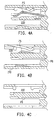
- FIG. 4A is a cross-sectional view of FIG. 3 cut along line A ⁇ A'.
- FIG. 4B is a cross-sectional view of FIG. 3 cut along line B ⁇ B'.
- FIG. 4C is a cross-sectional view of FIG. 3 cut along line C ⁇ C'.
- FIG. 1 is a diagram illustrating the pin lengths of a connector according to an embodiment of the present invention.
- the pin lengths of the connector are classified into 5, which are respectively L 1 ⁇ L 5 .
- the 11 pins P1 ⁇ P11 in the present embodiment are classified into 5 pin groups based on the pin lengths L 1 ⁇ L 5 thereof.
- the first pin group is ground pins including pins P5 and P10, which are referred to thereinafter as ground pins P5 and P10, and the pin length thereof is L 1 .
- the second pin group is audio pins including pins P6, P7, and P11, which are referred to thereinafter as audio pins P6, P7, and P11, and the pin length thereof is L 2 .
- the third pin group is power supply pin including only pin P1, which is referred to thereinafter as power supply pin P1, and the pin length thereof is L 3 .
- the fourth pin group is signal pins including pins P2, P3, and P4, which are referred to thereinafter as signal pins P2, P3, and P4, and the pin length thereof is L 4 .
- the fifth pin group is data pins including pins P8 and P9, which are referred to thereinafter as data pins P8 and P9, and the pin length thereof is L 5 .
- L 1 , L 2 , L 3 , L 4 , and L 5 are all positive integers and L 1 >L 2 >L 3 >L 4 >L 5 .
- the pins P1 ⁇ P11 are classified into 5 different lengths, wherein the pin length L 1 of the ground pins P5 and P10 is the longest.
- the ground pins P5 and P10 always connect the peripheral device and the host first regardless from which direction the user inserts the connector into the host, so that a common ground voltage level can be built up first between the host and the peripheral device to avoid signal misjudgment due to different user habit or working environment.
- the audio pins P6, P7, and P11 are mainly for transmitting audio signals and the pin length L 2 thereof is slightly smaller than the pin length L 1 of the ground pins P5 and P10. Besides, the ground voltage level required for signal transmission by the audio pins P6, P7, and P11 can be connected to the ground terminal along with the ground pin P10 through an independent path so as to reduce noise interference.
- the audio pin P6 when the peripheral device performs the function of a microphone, the audio pin P6 provides a transmission path for the audio signals of the microphone. If the peripheral device performs the function of a speaker or an earphone, the audio pin P7 provides a transmission path for right-channel audio signals, while the audio pin P11 provides a transmission path for left-channel audio signals.
- the data pins P8 and P9 are mainly used for providing a digital signal transmission path between the peripheral device and the host, and the pin length L 5 thereof is the shortest.
- the data pin P9 provides a clock signal transmission path, and the peripheral device can transmit a device data to the host or the device data can be transmitted from the host to the peripheral device along with the clock signal through the data pin P8.
- the host determines the type of the peripheral device according to the device data and controls the peripheral device through data transmission.
- the aggregation of the ground pin P5, the power supply pin P1, and the signal pins P2, P3, P4 has the function of connecting a USB interface and the ground pin P5, the power supply pin P1, and the signal pins P2, P3, P4 are disposed on the same surface of the connector.
- the power supply pin P1 provides the transmission path of the voltage source
- the signal pins P2 and P3 provide the transmission path for differential signals in the USB
- the signal pin P4 is used for determining the master-slave relationship between the host and the peripheral device during signal transmission based on the voltage level thereof.
- FIG. 2 is a cross-sectional view illustrating the structure of a connector according to the present embodiment.
- the pins P1 ⁇ P5 are disposed on the same surface of the connector 200, which is referred to as the top surface of the insulating layer 220 in the present embodiment.
- the pins P6 ⁇ P11 are disposed on another side of the connector 200, which is referred to as the bottom surface of the insulating layer 220 in the present embodiment.
- the outside of the connector 200 is surrounded by a case 210.
- the insulating layer 220 isolates the pins P1 ⁇ P5 and the pins P6 ⁇ P11.
- the connector 200 is connected to a host through a printed circuit board.
- the host can be a PDA, smart cell phone, GPS device, music player, and game machine.
- FIG. 3 is a cross-sectional view illustrating the major pins of a connector according to the present embodiment.
- the cross-sectional view thereof cut along line A-A' is as shown in FIG. 4A, wherein the signal pin P3 is disposed on the top surface of the insulating layer 220.
- the audio pin P6 as example, the cross-sectional view thereof cut along line B ⁇ B' is as shown in FIG. 4B, wherein the ground pin P5 and the audio pin P6 are respectively disposed on the top and bottom surface of the insulating layer 220.
- the ground pin P5 is closer to the opening of the case 210 than the audio pin P6, so that the ground pin P5 can first come into contact with the corresponding pin of the socket when the connector 200 is connected to the socket.
- the data pin P8 as example, the cross-sectional view thereof cut along line C-C' is as shown in FIG. 4C, wherein the data pin P8 is disposed on the bottom surface of the insulating layer 220.
- FIG. 4A-4A are cross-sectional views illustrating the major pin structures according to the present embodiment.
- the present invention is not limited to these structures. Even the present invention has bee explained with 5 pin lengths as example, the present invention can be applied to connectors of various pin lengths.
- the other workable connector structures should be easily understood by those having ordinary skill in the art and therefore will not be described herein.
- pin functions of the present invention are not limited thereto.
- the applications of the present invention in connectors of different pin functions or transmission interfaces can be easily understood based on the present disclosure by those having ordinary knowledge in the art, therefore will not be described herein.
- pins of different lengths are used for different pin functions so that signal misjudgment due to different user habit or working environment can be effectively avoided.
- the functions of various connectors can be integrated into one single connector so that the space and design cost of hand-held electronic devices can be effectively reduced.
Landscapes
- Details Of Connecting Devices For Male And Female Coupling (AREA)
- Coupling Device And Connection With Printed Circuit (AREA)
Abstract
Description
- The present invention relates to a connector. More particularly, the present invention relates to a connector having different pin lengths.
- Universal serial bus (USB) is usually used as the interface for transmitting digital signals, and as to some commonly used peripheral devices, such as earphones and speakers, to improve audio quality and simplify design, independent connectors are generally used for transmitting data and for differentiating the peripheral devices. However, as to those hand-held devices whose designs are going towards being light, thin, short, compact and small, such as mobile phones, personal digital assistants (PDAs), smart phones, GPS devices, music players, and game machines, the cost and the volumes thereof may be increased if various connectors are to be disposed therein.
- Generally, the pin lengths of a connector are the same, the angle of inserting the connector is different when the user habit and the working environment are different. Signal misjudgment may be caused if the pin connection sequence in the connector is not consistent, for example, if the pin for transmitting signal is connected before the ground pin, signal misjudgment will be caused due to a lack of ground voltage level.
- Accordingly, the present invention is directed to provide a connector which is suitable for both USB and audio signal transmissions.
- According to another aspect of the present invention, a connector is provided, wherein USB pins and audio signal pins are integrated into an insulating layer, so as to integrate the functions of various connectors.
- According to yet another aspect of the present invention, a connector is provided, wherein pins of different lengths are disposed according to different functions so that the connector can be applied to different insertion angles, accordingly the accuracy of signal transmission is improved and signal misjudgment is avoided.
- To achieve the aforementioned and other aspects , the present invention provides a connector for connecting a host and a peripheral device. The connector includes N pin groups and each of the pin groups has different pin length, wherein N is a positive integer and is greater than or equal to 3.
- According to a connector in an embodiment of the present invention, if N is equal to 5, the connector includes 5 pin groups, the pin lengths of the pin groups are respectively L1~L5. Wherein L1, L2, L3, L4, L5 are all positive integers, and L1>L2>L3>L4>L5.
- To achieve the aforementioned and other aspects, the present invention provides a connector for connecting a host and a peripheral device. The connector includes two ground pins, three audio pins, a power supply pin, three signal pins, and two data pins. Wherein, the length of the ground pins is L1, the length of the audio pins is L2, the length of the power supply pin is L3, the length of the signal pins is L4, and the length of the data pins is L5. Wherein, L1, L2, L3, L4, L5 are all positive integers and L1>L2>L3>L4>L5.
- To achieve the aforementioned and other aspects, the present invention provides a connector for connecting a host and a peripheral device. The connector includes an insulating layer having a top surface and a bottom surface and N pin groups respectively disposed, on the top surface and the bottom surface, wherein each of the pin groups has different pin length, N is a positive integer and N is greater than or equal to 3.
- According to a connector in an embodiment of the present invention, if N is equal to 5, the connector includes 5 pin groups, and the pin lengths of the 5 pin groups are respectively L1~L5. Wherein L1, L2, L3, L4, L5 are all positive integers and L1>L2>L3>L4>L5.
- In overview, multiple pins are adopted in the present invention to integrate USB and audio signal transmission interfaces into a connector so that a single connector can perform more functions, accordingly, the number of connectors and the space required by the connectors in an electronic apparatus can be reduced. Meanwhile, pins of different lengths are disposed according to different functions so that the connector can be applied to different insertion angles, accordingly, the accuracy of signal transmission is increased and signal misjudgment is avoided.
- In order to make the aforementioned and other aspects, features and advantages of the present invention comprehensible, a preferred embodiment accompanied with figures is described in detail below.
- It is to be understood that both the foregoing general description and the following detailed description are exemplary, and are intended to provide further explanation of the invention as claimed.
- The accompanying drawings are included to provide a further understanding of the invention, and are incorporated in and constitute a part of this specification. The drawings illustrate embodiments of the invention and, together with the description, serve to explain the principles of the invention.
- FIG. 1 is a diagram illustrating the pin lengths of a connector according to an embodiment of the present invention.
- FIG. 2 is a cross-sectional view illustrating the structure of a connector according to an embodiment of the present invention.
- FIG. 3 is a cross-sectional view illustrating the major pins of a connector according to an embodiment of the present invention.
- FIG. 4A is a cross-sectional view of FIG. 3 cut along line A~A'.
- FIG. 4B is a cross-sectional view of FIG. 3 cut along line B~B'.
- FIG. 4C is a cross-sectional view of FIG. 3 cut along line C~C'.
- FIG. 1 is a diagram illustrating the pin lengths of a connector according to an embodiment of the present invention. In the present embodiment, the pin lengths of the connector are classified into 5, which are respectively L1~L5. The 11 pins P1~P11 in the present embodiment are classified into 5 pin groups based on the pin lengths L1~L5 thereof. The first pin group is ground pins including pins P5 and P10, which are referred to thereinafter as ground pins P5 and P10, and the pin length thereof is L1. The second pin group is audio pins including pins P6, P7, and P11, which are referred to thereinafter as audio pins P6, P7, and P11, and the pin length thereof is L2. The third pin group is power supply pin including only pin P1, which is referred to thereinafter as power supply pin P1, and the pin length thereof is L3. The fourth pin group is signal pins including pins P2, P3, and P4, which are referred to thereinafter as signal pins P2, P3, and P4, and the pin length thereof is L4. The fifth pin group is data pins including pins P8 and P9, which are referred to thereinafter as data pins P8 and P9, and the pin length thereof is L5. Wherein L1, L2, L3, L4, and L5 are all positive integers and L1>L2>L3>L4>L5.
- In the present embodiment, the pins P1~P11 are classified into 5 different lengths, wherein the pin length L1 of the ground pins P5 and P10 is the longest. Thus, during normal operation, the ground pins P5 and P10 always connect the peripheral device and the host first regardless from which direction the user inserts the connector into the host, so that a common ground voltage level can be built up first between the host and the peripheral device to avoid signal misjudgment due to different user habit or working environment.
- To transmit audio signals more effectively, the audio pins P6, P7, and P11 are mainly for transmitting audio signals and the pin length L2 thereof is slightly smaller than the pin length L1 of the ground pins P5 and P10. Besides, the ground voltage level required for signal transmission by the audio pins P6, P7, and P11 can be connected to the ground terminal along with the ground pin P10 through an independent path so as to reduce noise interference. Wherein, when the peripheral device performs the function of a microphone, the audio pin P6 provides a transmission path for the audio signals of the microphone. If the peripheral device performs the function of a speaker or an earphone, the audio pin P7 provides a transmission path for right-channel audio signals, while the audio pin P11 provides a transmission path for left-channel audio signals.
- The data pins P8 and P9 are mainly used for providing a digital signal transmission path between the peripheral device and the host, and the pin length L5 thereof is the shortest. The data pin P9 provides a clock signal transmission path, and the peripheral device can transmit a device data to the host or the device data can be transmitted from the host to the peripheral device along with the clock signal through the data pin P8. The host determines the type of the peripheral device according to the device data and controls the peripheral device through data transmission.
- In the usage of the connector, the aggregation of the ground pin P5, the power supply pin P1, and the signal pins P2, P3, P4 has the function of connecting a USB interface and the ground pin P5, the power supply pin P1, and the signal pins P2, P3, P4 are disposed on the same surface of the connector. Wherein the power supply pin P1 provides the transmission path of the voltage source, the signal pins P2 and P3 provide the transmission path for differential signals in the USB, and the signal pin P4 is used for determining the master-slave relationship between the host and the peripheral device during signal transmission based on the voltage level thereof. The aggregation of the ground pin P5, the power supply pin P1, and the signal pins P2, P3, P4 is compatible to the pin functions of a USB interface, only the relative pin lengths are described in the present embodiment, and the respective pin function thereof should be understood by those having ordinary skill in the art, therefore will not be described herein.
- FIG. 2 is a cross-sectional view illustrating the structure of a connector according to the present embodiment. The pins P1~P5 are disposed on the same surface of the
connector 200, which is referred to as the top surface of theinsulating layer 220 in the present embodiment. The pins P6~P11 are disposed on another side of theconnector 200, which is referred to as the bottom surface of theinsulating layer 220 in the present embodiment. The outside of theconnector 200 is surrounded by acase 210. Theinsulating layer 220 isolates the pins P1~P5 and the pins P6~P11. Theconnector 200 is connected to a host through a printed circuit board. In the present embodiment, the host can be a PDA, smart cell phone, GPS device, music player, and game machine. - Next, the structure of the connector in the present embodiment will be further described with cross-sectional views. FIG. 3 is a cross-sectional view illustrating the major pins of a connector according to the present embodiment. With the signal pin P3 as example, the cross-sectional view thereof cut along line A-A' is as shown in FIG. 4A, wherein the signal pin P3 is disposed on the top surface of the
insulating layer 220. With the audio pin P6 as example, the cross-sectional view thereof cut along line B~B' is as shown in FIG. 4B, wherein the ground pin P5 and the audio pin P6 are respectively disposed on the top and bottom surface of the insulatinglayer 220. Obviously, the ground pin P5 is closer to the opening of thecase 210 than the audio pin P6, so that the ground pin P5 can first come into contact with the corresponding pin of the socket when theconnector 200 is connected to the socket. With the data pin P8 as example, the cross-sectional view thereof cut along line C-C' is as shown in FIG. 4C, wherein the data pin P8 is disposed on the bottom surface of the insulatinglayer 220. - FIG. 4A-4A are cross-sectional views illustrating the major pin structures according to the present embodiment. However, the present invention is not limited to these structures. Even the present invention has bee explained with 5 pin lengths as example, the present invention can be applied to connectors of various pin lengths. The other workable connector structures should be easily understood by those having ordinary skill in the art and therefore will not be described herein.
- In overview, even though only one pin combination suitable for USB and audio signal is used as example in the present embodiment for describing the present invention, the pin functions of the present invention are not limited thereto. The applications of the present invention in connectors of different pin functions or transmission interfaces can be easily understood based on the present disclosure by those having ordinary knowledge in the art, therefore will not be described herein.
- According to the present invention, pins of different lengths are used for different pin functions so that signal misjudgment due to different user habit or working environment can be effectively avoided. Meanwhile, the functions of various connectors can be integrated into one single connector so that the space and design cost of hand-held electronic devices can be effectively reduced.
- It will be apparent to those skilled in the art that various modifications and variations can be made to the structure of the present invention without departing from the scope or spirit of the invention. In view of the foregoing, it is intended that the present invention cover modifications and variations of this invention provided they fall within the scope of the following claims and their equivalents.
Claims (10)
- A connector for connecting a host and a peripheral device, comprising at least:N pin groups, the pin length of each of the pin groups being different;wherein N is a positive integer and N is greater than or equal to 3.
- The connector claimed in claim 1, wherein if N is equal to 5, the connector comprises:a first pin group, the pin length of the first pin group being L1;a second pin group, the pin length of the second pin group being L2;a third pin group, the pin length of the third pin group being L3;a fourth pin group, the pin length of the fourth pin group being L4; anda fifth pin group, the pin length of the fifth pin group being L5;wherein L1, L2, L3, L4, L5 are all positive integers and L1>L2>L3>L4>L5
- The connector claimed in claim 2, wherein the first pin group comprises:a first ground pin, providing a coupling path between the peripheral device and a ground terminal cooperating with the signal transmission of the second pin group; anda second ground pin, providing another coupling path between the peripheral device and the ground terminal cooperating with the signal transmission of the fourth pin group;and the second pin group comprises:a first audio pin, providing a left-channel audio signal transmission path;a second audio pin, providing a right-channel audio signal transmission path; anda third audio pin, providing an audio signal transmission path for a microphone when the peripheral device is the microphone;and the third pin group comprises a power supply pin;and the fourth pin group comprises:two first signal pins, providing a differential signal transmission path; anda second signal pin, used for determining the master-slave relationship between the host and the peripheral device during signal transmission;and the fifth pin group comprises:a first data pin, providing a clock signal transmission path; anda second data pin, providing a device data transmission path cooperating with the clock signal;wherein the host determines the type of the peripheral device according to the device data.
- The connector claimed in claim 3, wherein the aggregation of the second ground pin, the third pin group, and the fourth pin group has the function of connecting a USB interface.
- A connector for connecting a host and a peripheral device, comprising:two ground pins, the pin length of each ground pin being L1;three audio pins, the pin length of each audio pin being L2;a power supply pin, the pin length of the power supply pin being L3;three signal pins, the pin length of each signal pin being L4; andtwo data pins, the pin length of each data pin being L5;wherein, L1, L2, L3, L4, L5 are all positive integers and L1>L2>L3>L4>L5.
- The connector claimed in claim 5, wherein the ground pins comprise:a first ground pin, providing a coupling path between the peripheral device and a ground terminal cooperating with the signal transmission of the audio pins; anda second ground pin, providing another coupling path between the peripheral device and the ground terminal cooperating with the signal transmission of the signal pins;and the audio pins comprise:a first audio pin, providing a left-channel audio signal transmission path;a second audio pin, providing a right-channel audio signal transmission path; anda third audio pin, providing an audio signal transmission path for a microphone when the peripheral device is the microphone;and the data pins comprise:a first data pin, providing a clock signal transmission path; anda second data pin, providing a device data transmission path cooperating with the clock signal;wherein the host determines the type of the peripheral device according to the device data.
- A connector for connecting a host and a peripheral device, comprising:an insulating layer, comprising a top surface and a bottom surface; andN pin groups, respectively disposed on the top surface and the bottom surface, the pin lengths of each of the pin groups being different;wherein N is a positive integer and N is greater than or equal to 3.
- The connector claimed in claim 7, wherein if N is equal to 5, the connector comprises:a first pin group, the pin length of the first pin group being L1;a second pin group, the pin length of the second pin group being L2;a third pin group, the pin length of the third pin group being L3;a fourth pin group, the pin length of the fourth pin group being L4; anda fifth pin group, the pin length of the fifth pin group being L5;wherein, L1, L2, L3, L4, L5 are all positive integers and L1>L2>L3>L4>L5.
- The connector claimed in claim 8, wherein the first pin group comprises:a first ground pin, providing a coupling path between the peripheral devicedevice and a ground terminal cooperating with the signal transmission of the second pin group; anda second ground pin, providing another coupling path between the peripheral devicedevice and the ground terminal cooperating with the signal transmission of the fourth pin group;and the second pin group comprises:a first audio pin, providing a left-channel audio signal transmission path;a second audio pin, providing a right-channel audio signal transmission path; anda third audio pin, providing an audio signal transmission path for a microphone when the peripheral devicedevice is the microphone;and the fifth pin group comprises:a first data pin, providing a clock signal transmission path; anda second data pin, providing a device data transmission path cooperating with the clock signal;wherein the host determines the type of the peripheral device according to the device data.
- The connector claimed in claim 9, wherein the aggregation of the second ground pin, the third pin group and the fourth pin group has the function of connecting a USB interface, and the second ground pin, the third pin group and the fourth pin group are all disposed on the top surface of the insulating layer, and the first ground pin, the second pin group and the fifth pin group are all disposed on the bottom surface of the insulating layer.
Applications Claiming Priority (1)
| Application Number | Priority Date | Filing Date | Title |
|---|---|---|---|
| CNB2006100813977A CN100539314C (en) | 2006-05-24 | 2006-05-24 | Connector |
Publications (2)
| Publication Number | Publication Date |
|---|---|
| EP1860739A1 true EP1860739A1 (en) | 2007-11-28 |
| EP1860739B1 EP1860739B1 (en) | 2010-04-14 |
Family
ID=38268797
Family Applications (1)
| Application Number | Title | Priority Date | Filing Date |
|---|---|---|---|
| EP07009324A Ceased EP1860739B1 (en) | 2006-05-24 | 2007-05-09 | Connector with contacts of different lengths |
Country Status (4)
| Country | Link |
|---|---|
| EP (1) | EP1860739B1 (en) |
| CN (1) | CN100539314C (en) |
| AT (1) | ATE464676T1 (en) |
| DE (1) | DE602007005864D1 (en) |
Cited By (2)
| Publication number | Priority date | Publication date | Assignee | Title |
|---|---|---|---|---|
| AU2009100658B4 (en) * | 2003-04-25 | 2009-10-01 | Apple Inc. | A female receptacle connector |
| US20150171575A1 (en) * | 2013-12-18 | 2015-06-18 | Ls Mtron Ltd. | Micro usb connector and electronic device including the same |
Families Citing this family (7)
| Publication number | Priority date | Publication date | Assignee | Title |
|---|---|---|---|---|
| JP2012208897A (en) * | 2011-03-30 | 2012-10-25 | Semiconductor Components Industries Llc | Input/output circuit |
| CN103107437A (en) * | 2013-01-17 | 2013-05-15 | 深圳市元征软件开发有限公司 | On-board diagnostics (OBD) connecting port protection structure |
| EP3381094B1 (en) * | 2016-02-29 | 2020-06-03 | SZ DJI Technology Co., Ltd. | Electrical connector |
| CN106207557A (en) * | 2016-07-18 | 2016-12-07 | 青岛海信电器股份有限公司 | A kind of female seat, male seat, main frame and expansion equipment |
| CN106549243B (en) * | 2016-12-07 | 2018-11-27 | 广东欧珀移动通信有限公司 | HDMI connector and Blu-ray player |
| CN108241408B (en) * | 2016-12-26 | 2021-02-12 | 神讯电脑(昆山)有限公司 | Electronic device and method for detecting connection direction of two electronic components |
| TWI802862B (en) | 2021-04-01 | 2023-05-21 | 華碩電腦股份有限公司 | Connector assembly and female connector |
Citations (1)
| Publication number | Priority date | Publication date | Assignee | Title |
|---|---|---|---|---|
| US6945824B1 (en) * | 2004-08-24 | 2005-09-20 | Cheng Uei Precision Industry Co., Ltd. | Connector assembly |
Family Cites Families (2)
| Publication number | Priority date | Publication date | Assignee | Title |
|---|---|---|---|---|
| CN2473770Y (en) * | 2001-03-28 | 2002-01-23 | 鸿松精密工业股份有限公司 | Connector structure |
| US6843686B2 (en) * | 2002-04-26 | 2005-01-18 | Honda Tsushin Kogyo Co., Ltd. | High-frequency electric connector having no ground terminals |
-
2006
- 2006-05-24 CN CNB2006100813977A patent/CN100539314C/en not_active Expired - Fee Related
-
2007
- 2007-05-09 AT AT07009324T patent/ATE464676T1/en not_active IP Right Cessation
- 2007-05-09 EP EP07009324A patent/EP1860739B1/en not_active Ceased
- 2007-05-09 DE DE602007005864T patent/DE602007005864D1/en active Active
Patent Citations (1)
| Publication number | Priority date | Publication date | Assignee | Title |
|---|---|---|---|---|
| US6945824B1 (en) * | 2004-08-24 | 2005-09-20 | Cheng Uei Precision Industry Co., Ltd. | Connector assembly |
Cited By (3)
| Publication number | Priority date | Publication date | Assignee | Title |
|---|---|---|---|---|
| AU2009100658B4 (en) * | 2003-04-25 | 2009-10-01 | Apple Inc. | A female receptacle connector |
| US20150171575A1 (en) * | 2013-12-18 | 2015-06-18 | Ls Mtron Ltd. | Micro usb connector and electronic device including the same |
| US9343859B2 (en) * | 2013-12-18 | 2016-05-17 | Ls Mtron Ltd. | Micro USB connector and electronic device including the same |
Also Published As
| Publication number | Publication date |
|---|---|
| ATE464676T1 (en) | 2010-04-15 |
| DE602007005864D1 (en) | 2010-05-27 |
| CN101079522A (en) | 2007-11-28 |
| EP1860739B1 (en) | 2010-04-14 |
| CN100539314C (en) | 2009-09-09 |
Similar Documents
| Publication | Publication Date | Title |
|---|---|---|
| US7448917B2 (en) | Connector having pin groups with different pin lengths | |
| EP1860739B1 (en) | Connector with contacts of different lengths | |
| US7427214B2 (en) | Compatible connector for first and second joints having different pin quantities | |
| US7544089B2 (en) | Adapter for USB and audio interface | |
| CN104620567B (en) | System and method for detecting ground and microphone input contacts in an audio plug | |
| US7833066B2 (en) | Earphone jack device and portable electronic device employing the same | |
| US7670181B2 (en) | Connector for first and second joints having different pin quantities, electronic apparatus with connector and combination | |
| CN103368014B (en) | Electrical Connectors and Handheld Electronic Devices | |
| US20210351601A1 (en) | Wireless sound output device with charging function | |
| US8976510B2 (en) | Cable assembly and electronic device | |
| CN101207256B (en) | An audio signal switching device | |
| EP2860827B1 (en) | High digital bandwidth connection apparatus | |
| US20080274647A1 (en) | Usb Data-Audio Signal Multiplexing Transmission Line | |
| US20130065448A1 (en) | Electronic connector | |
| CN205319383U (en) | Improved connector | |
| EP1860746B1 (en) | Compatible connector for first and second joints having different pin quantities | |
| US11611177B2 (en) | USB type-C male connector | |
| KR20090042375A (en) | USB plug, AV socket for USB plug and USB connector device having same | |
| US20080096434A1 (en) | Microphone Connector | |
| JP3145665U (en) | Socket connector | |
| US20110294310A1 (en) | Memory card and memory card holding structure | |
| CN202424706U (en) | Wireless transmission device with external antenna | |
| CN209993761U (en) | Terminal block and connector thereof with insert card assembly part | |
| CN106785532A (en) | Composite connector | |
| CN105100986A (en) | Audio transmission device |
Legal Events
| Date | Code | Title | Description |
|---|---|---|---|
| PUAI | Public reference made under article 153(3) epc to a published international application that has entered the european phase |
Free format text: ORIGINAL CODE: 0009012 |
|
| AK | Designated contracting states |
Kind code of ref document: A1 Designated state(s): AT BE BG CH CY CZ DE DK EE ES FI FR GB GR HU IE IS IT LI LT LU LV MC MT NL PL PT RO SE SI SK TR |
|
| AX | Request for extension of the european patent |
Extension state: AL BA HR MK YU |
|
| 17P | Request for examination filed |
Effective date: 20080526 |
|
| AKX | Designation fees paid |
Designated state(s): AT BE BG CH CY CZ DE DK EE ES FI FR GB GR HU IE IS IT LI LT LU LV MC MT NL PL PT RO SE SI SK TR |
|
| 17Q | First examination report despatched |
Effective date: 20081027 |
|
| RAP1 | Party data changed (applicant data changed or rights of an application transferred) |
Owner name: HTC CORPORATION |
|
| GRAP | Despatch of communication of intention to grant a patent |
Free format text: ORIGINAL CODE: EPIDOSNIGR1 |
|
| GRAJ | Information related to disapproval of communication of intention to grant by the applicant or resumption of examination proceedings by the epo deleted |
Free format text: ORIGINAL CODE: EPIDOSDIGR1 |
|
| GRAP | Despatch of communication of intention to grant a patent |
Free format text: ORIGINAL CODE: EPIDOSNIGR1 |
|
| GRAS | Grant fee paid |
Free format text: ORIGINAL CODE: EPIDOSNIGR3 |
|
| GRAA | (expected) grant |
Free format text: ORIGINAL CODE: 0009210 |
|
| AK | Designated contracting states |
Kind code of ref document: B1 Designated state(s): AT BE BG CH CY CZ DE DK EE ES FI FR GB GR HU IE IS IT LI LT LU LV MC MT NL PL PT RO SE SI SK TR |
|
| REG | Reference to a national code |
Ref country code: GB Ref legal event code: FG4D |
|
| REG | Reference to a national code |
Ref country code: CH Ref legal event code: EP |
|
| REG | Reference to a national code |
Ref country code: IE Ref legal event code: FG4D |
|
| REF | Corresponds to: |
Ref document number: 602007005864 Country of ref document: DE Date of ref document: 20100527 Kind code of ref document: P |
|
| REG | Reference to a national code |
Ref country code: NL Ref legal event code: T3 |
|
| LTIE | Lt: invalidation of european patent or patent extension |
Effective date: 20100414 |
|
| PG25 | Lapsed in a contracting state [announced via postgrant information from national office to epo] |
Ref country code: SE Free format text: LAPSE BECAUSE OF FAILURE TO SUBMIT A TRANSLATION OF THE DESCRIPTION OR TO PAY THE FEE WITHIN THE PRESCRIBED TIME-LIMIT Effective date: 20100414 Ref country code: LT Free format text: LAPSE BECAUSE OF FAILURE TO SUBMIT A TRANSLATION OF THE DESCRIPTION OR TO PAY THE FEE WITHIN THE PRESCRIBED TIME-LIMIT Effective date: 20100414 Ref country code: ES Free format text: LAPSE BECAUSE OF FAILURE TO SUBMIT A TRANSLATION OF THE DESCRIPTION OR TO PAY THE FEE WITHIN THE PRESCRIBED TIME-LIMIT Effective date: 20100725 |
|
| PG25 | Lapsed in a contracting state [announced via postgrant information from national office to epo] |
Ref country code: IS Free format text: LAPSE BECAUSE OF FAILURE TO SUBMIT A TRANSLATION OF THE DESCRIPTION OR TO PAY THE FEE WITHIN THE PRESCRIBED TIME-LIMIT Effective date: 20100814 Ref country code: FI Free format text: LAPSE BECAUSE OF FAILURE TO SUBMIT A TRANSLATION OF THE DESCRIPTION OR TO PAY THE FEE WITHIN THE PRESCRIBED TIME-LIMIT Effective date: 20100414 Ref country code: AT Free format text: LAPSE BECAUSE OF FAILURE TO SUBMIT A TRANSLATION OF THE DESCRIPTION OR TO PAY THE FEE WITHIN THE PRESCRIBED TIME-LIMIT Effective date: 20100414 Ref country code: SI Free format text: LAPSE BECAUSE OF FAILURE TO SUBMIT A TRANSLATION OF THE DESCRIPTION OR TO PAY THE FEE WITHIN THE PRESCRIBED TIME-LIMIT Effective date: 20100414 Ref country code: LV Free format text: LAPSE BECAUSE OF FAILURE TO SUBMIT A TRANSLATION OF THE DESCRIPTION OR TO PAY THE FEE WITHIN THE PRESCRIBED TIME-LIMIT Effective date: 20100414 |
|
| PG25 | Lapsed in a contracting state [announced via postgrant information from national office to epo] |
Ref country code: CY Free format text: LAPSE BECAUSE OF FAILURE TO SUBMIT A TRANSLATION OF THE DESCRIPTION OR TO PAY THE FEE WITHIN THE PRESCRIBED TIME-LIMIT Effective date: 20100519 Ref country code: MC Free format text: LAPSE BECAUSE OF NON-PAYMENT OF DUE FEES Effective date: 20100531 Ref country code: PL Free format text: LAPSE BECAUSE OF FAILURE TO SUBMIT A TRANSLATION OF THE DESCRIPTION OR TO PAY THE FEE WITHIN THE PRESCRIBED TIME-LIMIT Effective date: 20100414 |
|
| PG25 | Lapsed in a contracting state [announced via postgrant information from national office to epo] |
Ref country code: PT Free format text: LAPSE BECAUSE OF FAILURE TO SUBMIT A TRANSLATION OF THE DESCRIPTION OR TO PAY THE FEE WITHIN THE PRESCRIBED TIME-LIMIT Effective date: 20100816 Ref country code: GR Free format text: LAPSE BECAUSE OF FAILURE TO SUBMIT A TRANSLATION OF THE DESCRIPTION OR TO PAY THE FEE WITHIN THE PRESCRIBED TIME-LIMIT Effective date: 20100715 Ref country code: EE Free format text: LAPSE BECAUSE OF FAILURE TO SUBMIT A TRANSLATION OF THE DESCRIPTION OR TO PAY THE FEE WITHIN THE PRESCRIBED TIME-LIMIT Effective date: 20100414 Ref country code: DK Free format text: LAPSE BECAUSE OF FAILURE TO SUBMIT A TRANSLATION OF THE DESCRIPTION OR TO PAY THE FEE WITHIN THE PRESCRIBED TIME-LIMIT Effective date: 20100414 |
|
| PLBE | No opposition filed within time limit |
Free format text: ORIGINAL CODE: 0009261 |
|
| STAA | Information on the status of an ep patent application or granted ep patent |
Free format text: STATUS: NO OPPOSITION FILED WITHIN TIME LIMIT |
|
| PG25 | Lapsed in a contracting state [announced via postgrant information from national office to epo] |
Ref country code: CZ Free format text: LAPSE BECAUSE OF FAILURE TO SUBMIT A TRANSLATION OF THE DESCRIPTION OR TO PAY THE FEE WITHIN THE PRESCRIBED TIME-LIMIT Effective date: 20100414 Ref country code: SK Free format text: LAPSE BECAUSE OF FAILURE TO SUBMIT A TRANSLATION OF THE DESCRIPTION OR TO PAY THE FEE WITHIN THE PRESCRIBED TIME-LIMIT Effective date: 20100414 Ref country code: RO Free format text: LAPSE BECAUSE OF FAILURE TO SUBMIT A TRANSLATION OF THE DESCRIPTION OR TO PAY THE FEE WITHIN THE PRESCRIBED TIME-LIMIT Effective date: 20100414 Ref country code: BE Free format text: LAPSE BECAUSE OF FAILURE TO SUBMIT A TRANSLATION OF THE DESCRIPTION OR TO PAY THE FEE WITHIN THE PRESCRIBED TIME-LIMIT Effective date: 20100414 |
|
| 26N | No opposition filed |
Effective date: 20110117 |
|
| PG25 | Lapsed in a contracting state [announced via postgrant information from national office to epo] |
Ref country code: IT Free format text: LAPSE BECAUSE OF NON-PAYMENT OF DUE FEES Effective date: 20100509 |
|
| PG25 | Lapsed in a contracting state [announced via postgrant information from national office to epo] |
Ref country code: IE Free format text: LAPSE BECAUSE OF NON-PAYMENT OF DUE FEES Effective date: 20100509 Ref country code: MT Free format text: LAPSE BECAUSE OF FAILURE TO SUBMIT A TRANSLATION OF THE DESCRIPTION OR TO PAY THE FEE WITHIN THE PRESCRIBED TIME-LIMIT Effective date: 20100414 |
|
| REG | Reference to a national code |
Ref country code: CH Ref legal event code: PL |
|
| PG25 | Lapsed in a contracting state [announced via postgrant information from national office to epo] |
Ref country code: CH Free format text: LAPSE BECAUSE OF NON-PAYMENT OF DUE FEES Effective date: 20110531 Ref country code: LI Free format text: LAPSE BECAUSE OF NON-PAYMENT OF DUE FEES Effective date: 20110531 |
|
| PG25 | Lapsed in a contracting state [announced via postgrant information from national office to epo] |
Ref country code: LU Free format text: LAPSE BECAUSE OF NON-PAYMENT OF DUE FEES Effective date: 20100509 Ref country code: HU Free format text: LAPSE BECAUSE OF FAILURE TO SUBMIT A TRANSLATION OF THE DESCRIPTION OR TO PAY THE FEE WITHIN THE PRESCRIBED TIME-LIMIT Effective date: 20101015 Ref country code: BG Free format text: LAPSE BECAUSE OF FAILURE TO SUBMIT A TRANSLATION OF THE DESCRIPTION OR TO PAY THE FEE WITHIN THE PRESCRIBED TIME-LIMIT Effective date: 20100414 |
|
| PG25 | Lapsed in a contracting state [announced via postgrant information from national office to epo] |
Ref country code: TR Free format text: LAPSE BECAUSE OF FAILURE TO SUBMIT A TRANSLATION OF THE DESCRIPTION OR TO PAY THE FEE WITHIN THE PRESCRIBED TIME-LIMIT Effective date: 20100414 |
|
| PG25 | Lapsed in a contracting state [announced via postgrant information from national office to epo] |
Ref country code: BG Free format text: LAPSE BECAUSE OF FAILURE TO SUBMIT A TRANSLATION OF THE DESCRIPTION OR TO PAY THE FEE WITHIN THE PRESCRIBED TIME-LIMIT Effective date: 20100714 |
|
| REG | Reference to a national code |
Ref country code: FR Ref legal event code: PLFP Year of fee payment: 9 |
|
| REG | Reference to a national code |
Ref country code: FR Ref legal event code: PLFP Year of fee payment: 10 |
|
| REG | Reference to a national code |
Ref country code: FR Ref legal event code: PLFP Year of fee payment: 11 |
|
| REG | Reference to a national code |
Ref country code: FR Ref legal event code: PLFP Year of fee payment: 12 |
|
| PGFP | Annual fee paid to national office [announced via postgrant information from national office to epo] |
Ref country code: NL Payment date: 20190515 Year of fee payment: 13 |
|
| PGFP | Annual fee paid to national office [announced via postgrant information from national office to epo] |
Ref country code: DE Payment date: 20190423 Year of fee payment: 13 Ref country code: IT Payment date: 20190527 Year of fee payment: 13 |
|
| PGFP | Annual fee paid to national office [announced via postgrant information from national office to epo] |
Ref country code: FR Payment date: 20190410 Year of fee payment: 13 |
|
| PGFP | Annual fee paid to national office [announced via postgrant information from national office to epo] |
Ref country code: GB Payment date: 20190508 Year of fee payment: 13 |
|
| REG | Reference to a national code |
Ref country code: DE Ref legal event code: R119 Ref document number: 602007005864 Country of ref document: DE |
|
| REG | Reference to a national code |
Ref country code: NL Ref legal event code: MM Effective date: 20200601 |
|
| PG25 | Lapsed in a contracting state [announced via postgrant information from national office to epo] |
Ref country code: NL Free format text: LAPSE BECAUSE OF NON-PAYMENT OF DUE FEES Effective date: 20200601 |
|
| GBPC | Gb: european patent ceased through non-payment of renewal fee |
Effective date: 20200509 |
|
| PG25 | Lapsed in a contracting state [announced via postgrant information from national office to epo] |
Ref country code: GB Free format text: LAPSE BECAUSE OF NON-PAYMENT OF DUE FEES Effective date: 20200509 Ref country code: FR Free format text: LAPSE BECAUSE OF NON-PAYMENT OF DUE FEES Effective date: 20200531 |
|
| PG25 | Lapsed in a contracting state [announced via postgrant information from national office to epo] |
Ref country code: DE Free format text: LAPSE BECAUSE OF NON-PAYMENT OF DUE FEES Effective date: 20201201 |
|
| PG25 | Lapsed in a contracting state [announced via postgrant information from national office to epo] |
Ref country code: IT Free format text: LAPSE BECAUSE OF NON-PAYMENT OF DUE FEES Effective date: 20200509 |