EP1860697A2 - Semiconductor device - Google Patents
Semiconductor device Download PDFInfo
- Publication number
- EP1860697A2 EP1860697A2 EP07008986A EP07008986A EP1860697A2 EP 1860697 A2 EP1860697 A2 EP 1860697A2 EP 07008986 A EP07008986 A EP 07008986A EP 07008986 A EP07008986 A EP 07008986A EP 1860697 A2 EP1860697 A2 EP 1860697A2
- Authority
- EP
- European Patent Office
- Prior art keywords
- semiconductor device
- electrical connections
- insulator substrate
- semiconductor chip
- sealing material
- Prior art date
- Legal status (The legal status is an assumption and is not a legal conclusion. Google has not performed a legal analysis and makes no representation as to the accuracy of the status listed.)
- Withdrawn
Links
Images


Classifications
-
- H—ELECTRICITY
- H10—SEMICONDUCTOR DEVICES; ELECTRIC SOLID-STATE DEVICES NOT OTHERWISE PROVIDED FOR
- H10W—GENERIC PACKAGES, INTERCONNECTIONS, CONNECTORS OR OTHER CONSTRUCTIONAL DETAILS OF DEVICES COVERED BY CLASS H10
- H10W42/00—Arrangements for protection of devices
-
- H—ELECTRICITY
- H10—SEMICONDUCTOR DEVICES; ELECTRIC SOLID-STATE DEVICES NOT OTHERWISE PROVIDED FOR
- H10W—GENERIC PACKAGES, INTERCONNECTIONS, CONNECTORS OR OTHER CONSTRUCTIONAL DETAILS OF DEVICES COVERED BY CLASS H10
- H10W42/00—Arrangements for protection of devices
- H10W42/60—Arrangements for protection of devices protecting against electrostatic charges or discharges, e.g. Faraday shields
-
- H—ELECTRICITY
- H10—SEMICONDUCTOR DEVICES; ELECTRIC SOLID-STATE DEVICES NOT OTHERWISE PROVIDED FOR
- H10W—GENERIC PACKAGES, INTERCONNECTIONS, CONNECTORS OR OTHER CONSTRUCTIONAL DETAILS OF DEVICES COVERED BY CLASS H10
- H10W76/00—Containers; Fillings or auxiliary members therefor; Seals
- H10W76/40—Fillings or auxiliary members in containers, e.g. centering rings
- H10W76/42—Fillings
- H10W76/47—Solid or gel fillings
-
- H—ELECTRICITY
- H10—SEMICONDUCTOR DEVICES; ELECTRIC SOLID-STATE DEVICES NOT OTHERWISE PROVIDED FOR
- H10W—GENERIC PACKAGES, INTERCONNECTIONS, CONNECTORS OR OTHER CONSTRUCTIONAL DETAILS OF DEVICES COVERED BY CLASS H10
- H10W90/00—Package configurations
-
- H—ELECTRICITY
- H10—SEMICONDUCTOR DEVICES; ELECTRIC SOLID-STATE DEVICES NOT OTHERWISE PROVIDED FOR
- H10D—INORGANIC ELECTRIC SEMICONDUCTOR DEVICES
- H10D62/00—Semiconductor bodies, or regions thereof, of devices having potential barriers
- H10D62/10—Shapes, relative sizes or dispositions of the regions of the semiconductor bodies; Shapes of the semiconductor bodies
- H10D62/102—Constructional design considerations for preventing surface leakage or controlling electric field concentration
- H10D62/103—Constructional design considerations for preventing surface leakage or controlling electric field concentration for increasing or controlling the breakdown voltage of reverse-biased devices
- H10D62/105—Constructional design considerations for preventing surface leakage or controlling electric field concentration for increasing or controlling the breakdown voltage of reverse-biased devices by having particular doping profiles, shapes or arrangements of PN junctions; by having supplementary regions, e.g. junction termination extension [JTE]
- H10D62/106—Constructional design considerations for preventing surface leakage or controlling electric field concentration for increasing or controlling the breakdown voltage of reverse-biased devices by having particular doping profiles, shapes or arrangements of PN junctions; by having supplementary regions, e.g. junction termination extension [JTE] having supplementary regions doped oppositely to or in rectifying contact with regions of the semiconductor bodies, e.g. guard rings with PN or Schottky junctions
-
- H—ELECTRICITY
- H10—SEMICONDUCTOR DEVICES; ELECTRIC SOLID-STATE DEVICES NOT OTHERWISE PROVIDED FOR
- H10W—GENERIC PACKAGES, INTERCONNECTIONS, CONNECTORS OR OTHER CONSTRUCTIONAL DETAILS OF DEVICES COVERED BY CLASS H10
- H10W72/00—Interconnections or connectors in packages
- H10W72/01—Manufacture or treatment
- H10W72/015—Manufacture or treatment of bond wires
- H10W72/01515—Forming coatings
-
- H—ELECTRICITY
- H10—SEMICONDUCTOR DEVICES; ELECTRIC SOLID-STATE DEVICES NOT OTHERWISE PROVIDED FOR
- H10W—GENERIC PACKAGES, INTERCONNECTIONS, CONNECTORS OR OTHER CONSTRUCTIONAL DETAILS OF DEVICES COVERED BY CLASS H10
- H10W72/00—Interconnections or connectors in packages
- H10W72/30—Die-attach connectors
- H10W72/351—Materials of die-attach connectors
- H10W72/352—Materials of die-attach connectors comprising metals or metalloids, e.g. solders
-
- H—ELECTRICITY
- H10—SEMICONDUCTOR DEVICES; ELECTRIC SOLID-STATE DEVICES NOT OTHERWISE PROVIDED FOR
- H10W—GENERIC PACKAGES, INTERCONNECTIONS, CONNECTORS OR OTHER CONSTRUCTIONAL DETAILS OF DEVICES COVERED BY CLASS H10
- H10W72/00—Interconnections or connectors in packages
- H10W72/50—Bond wires
- H10W72/521—Structures or relative sizes of bond wires
- H10W72/522—Multilayered bond wires, e.g. having a coating concentric around a core
-
- H—ELECTRICITY
- H10—SEMICONDUCTOR DEVICES; ELECTRIC SOLID-STATE DEVICES NOT OTHERWISE PROVIDED FOR
- H10W—GENERIC PACKAGES, INTERCONNECTIONS, CONNECTORS OR OTHER CONSTRUCTIONAL DETAILS OF DEVICES COVERED BY CLASS H10
- H10W72/00—Interconnections or connectors in packages
- H10W72/50—Bond wires
- H10W72/521—Structures or relative sizes of bond wires
- H10W72/522—Multilayered bond wires, e.g. having a coating concentric around a core
- H10W72/523—Multilayered bond wires, e.g. having a coating concentric around a core characterised by the structures of the outermost layers, e.g. multilayered coatings
-
- H—ELECTRICITY
- H10—SEMICONDUCTOR DEVICES; ELECTRIC SOLID-STATE DEVICES NOT OTHERWISE PROVIDED FOR
- H10W—GENERIC PACKAGES, INTERCONNECTIONS, CONNECTORS OR OTHER CONSTRUCTIONAL DETAILS OF DEVICES COVERED BY CLASS H10
- H10W72/00—Interconnections or connectors in packages
- H10W72/50—Bond wires
- H10W72/531—Shapes of wire connectors
- H10W72/5363—Shapes of wire connectors the connected ends being wedge-shaped
-
- H—ELECTRICITY
- H10—SEMICONDUCTOR DEVICES; ELECTRIC SOLID-STATE DEVICES NOT OTHERWISE PROVIDED FOR
- H10W—GENERIC PACKAGES, INTERCONNECTIONS, CONNECTORS OR OTHER CONSTRUCTIONAL DETAILS OF DEVICES COVERED BY CLASS H10
- H10W72/00—Interconnections or connectors in packages
- H10W72/50—Bond wires
- H10W72/541—Dispositions of bond wires
- H10W72/543—Dispositions of bond wires of outermost layers of multilayered bond wires, e.g. coating being only on a part of a core
-
- H—ELECTRICITY
- H10—SEMICONDUCTOR DEVICES; ELECTRIC SOLID-STATE DEVICES NOT OTHERWISE PROVIDED FOR
- H10W—GENERIC PACKAGES, INTERCONNECTIONS, CONNECTORS OR OTHER CONSTRUCTIONAL DETAILS OF DEVICES COVERED BY CLASS H10
- H10W72/00—Interconnections or connectors in packages
- H10W72/50—Bond wires
- H10W72/541—Dispositions of bond wires
- H10W72/5445—Dispositions of bond wires being orthogonal to a side surface of the chip, e.g. parallel arrangements
-
- H—ELECTRICITY
- H10—SEMICONDUCTOR DEVICES; ELECTRIC SOLID-STATE DEVICES NOT OTHERWISE PROVIDED FOR
- H10W—GENERIC PACKAGES, INTERCONNECTIONS, CONNECTORS OR OTHER CONSTRUCTIONAL DETAILS OF DEVICES COVERED BY CLASS H10
- H10W72/00—Interconnections or connectors in packages
- H10W72/50—Bond wires
- H10W72/551—Materials of bond wires
- H10W72/552—Materials of bond wires comprising metals or metalloids, e.g. silver
-
- H—ELECTRICITY
- H10—SEMICONDUCTOR DEVICES; ELECTRIC SOLID-STATE DEVICES NOT OTHERWISE PROVIDED FOR
- H10W—GENERIC PACKAGES, INTERCONNECTIONS, CONNECTORS OR OTHER CONSTRUCTIONAL DETAILS OF DEVICES COVERED BY CLASS H10
- H10W72/00—Interconnections or connectors in packages
- H10W72/50—Bond wires
- H10W72/551—Materials of bond wires
- H10W72/552—Materials of bond wires comprising metals or metalloids, e.g. silver
- H10W72/5522—Materials of bond wires comprising metals or metalloids, e.g. silver comprising gold [Au]
-
- H—ELECTRICITY
- H10—SEMICONDUCTOR DEVICES; ELECTRIC SOLID-STATE DEVICES NOT OTHERWISE PROVIDED FOR
- H10W—GENERIC PACKAGES, INTERCONNECTIONS, CONNECTORS OR OTHER CONSTRUCTIONAL DETAILS OF DEVICES COVERED BY CLASS H10
- H10W72/00—Interconnections or connectors in packages
- H10W72/50—Bond wires
- H10W72/551—Materials of bond wires
- H10W72/552—Materials of bond wires comprising metals or metalloids, e.g. silver
- H10W72/5524—Materials of bond wires comprising metals or metalloids, e.g. silver comprising aluminium [Al]
-
- H—ELECTRICITY
- H10—SEMICONDUCTOR DEVICES; ELECTRIC SOLID-STATE DEVICES NOT OTHERWISE PROVIDED FOR
- H10W—GENERIC PACKAGES, INTERCONNECTIONS, CONNECTORS OR OTHER CONSTRUCTIONAL DETAILS OF DEVICES COVERED BY CLASS H10
- H10W72/00—Interconnections or connectors in packages
- H10W72/50—Bond wires
- H10W72/551—Materials of bond wires
- H10W72/553—Materials of bond wires not comprising solid metals or solid metalloids, e.g. polymers, ceramics or liquids
-
- H—ELECTRICITY
- H10—SEMICONDUCTOR DEVICES; ELECTRIC SOLID-STATE DEVICES NOT OTHERWISE PROVIDED FOR
- H10W—GENERIC PACKAGES, INTERCONNECTIONS, CONNECTORS OR OTHER CONSTRUCTIONAL DETAILS OF DEVICES COVERED BY CLASS H10
- H10W72/00—Interconnections or connectors in packages
- H10W72/50—Bond wires
- H10W72/551—Materials of bond wires
- H10W72/555—Materials of bond wires of outermost layers of multilayered bond wires, e.g. material of a coating
-
- H—ELECTRICITY
- H10—SEMICONDUCTOR DEVICES; ELECTRIC SOLID-STATE DEVICES NOT OTHERWISE PROVIDED FOR
- H10W—GENERIC PACKAGES, INTERCONNECTIONS, CONNECTORS OR OTHER CONSTRUCTIONAL DETAILS OF DEVICES COVERED BY CLASS H10
- H10W72/00—Interconnections or connectors in packages
- H10W72/50—Bond wires
- H10W72/581—Auxiliary members, e.g. flow barriers
-
- H—ELECTRICITY
- H10—SEMICONDUCTOR DEVICES; ELECTRIC SOLID-STATE DEVICES NOT OTHERWISE PROVIDED FOR
- H10W—GENERIC PACKAGES, INTERCONNECTIONS, CONNECTORS OR OTHER CONSTRUCTIONAL DETAILS OF DEVICES COVERED BY CLASS H10
- H10W72/00—Interconnections or connectors in packages
- H10W72/50—Bond wires
- H10W72/59—Bond pads specially adapted therefor
-
- H—ELECTRICITY
- H10—SEMICONDUCTOR DEVICES; ELECTRIC SOLID-STATE DEVICES NOT OTHERWISE PROVIDED FOR
- H10W—GENERIC PACKAGES, INTERCONNECTIONS, CONNECTORS OR OTHER CONSTRUCTIONAL DETAILS OF DEVICES COVERED BY CLASS H10
- H10W90/00—Package configurations
- H10W90/701—Package configurations characterised by the relative positions of pads or connectors relative to package parts
- H10W90/731—Package configurations characterised by the relative positions of pads or connectors relative to package parts of die-attach connectors
- H10W90/734—Package configurations characterised by the relative positions of pads or connectors relative to package parts of die-attach connectors between a chip and a stacked insulating package substrate, interposer or RDL
-
- H—ELECTRICITY
- H10—SEMICONDUCTOR DEVICES; ELECTRIC SOLID-STATE DEVICES NOT OTHERWISE PROVIDED FOR
- H10W—GENERIC PACKAGES, INTERCONNECTIONS, CONNECTORS OR OTHER CONSTRUCTIONAL DETAILS OF DEVICES COVERED BY CLASS H10
- H10W90/00—Package configurations
- H10W90/701—Package configurations characterised by the relative positions of pads or connectors relative to package parts
- H10W90/751—Package configurations characterised by the relative positions of pads or connectors relative to package parts of bond wires
- H10W90/753—Package configurations characterised by the relative positions of pads or connectors relative to package parts of bond wires between laterally-adjacent chips
-
- H—ELECTRICITY
- H10—SEMICONDUCTOR DEVICES; ELECTRIC SOLID-STATE DEVICES NOT OTHERWISE PROVIDED FOR
- H10W—GENERIC PACKAGES, INTERCONNECTIONS, CONNECTORS OR OTHER CONSTRUCTIONAL DETAILS OF DEVICES COVERED BY CLASS H10
- H10W90/00—Package configurations
- H10W90/701—Package configurations characterised by the relative positions of pads or connectors relative to package parts
- H10W90/751—Package configurations characterised by the relative positions of pads or connectors relative to package parts of bond wires
- H10W90/754—Package configurations characterised by the relative positions of pads or connectors relative to package parts of bond wires between a chip and a stacked insulating package substrate, interposer or RDL
-
- H—ELECTRICITY
- H10—SEMICONDUCTOR DEVICES; ELECTRIC SOLID-STATE DEVICES NOT OTHERWISE PROVIDED FOR
- H10W—GENERIC PACKAGES, INTERCONNECTIONS, CONNECTORS OR OTHER CONSTRUCTIONAL DETAILS OF DEVICES COVERED BY CLASS H10
- H10W90/00—Package configurations
- H10W90/701—Package configurations characterised by the relative positions of pads or connectors relative to package parts
- H10W90/751—Package configurations characterised by the relative positions of pads or connectors relative to package parts of bond wires
- H10W90/756—Package configurations characterised by the relative positions of pads or connectors relative to package parts of bond wires between a chip and a stacked lead frame, conducting package substrate or heat sink
Definitions
- the present invention relates to a semiconductor device in which injection of electric charge from an electric charge source is restricted to provide highly reliable insulating performance.
- a structure having such a high withstand voltage retaining capability is obtained by use of a power semiconductor chip like an insulated-gate bipolar transistor (IGBT) and insulative sealing resin for packaging the power semiconductor chip, for example.
- IGBT insulated-gate bipolar transistor
- a guard ring structure which typically includes a plurality of guard rings separated from one another running along an outer peripheral region of an upper surface of a semiconductor chip and a plurality of capacitive elements made of an insulating material like sealing resin filled between the adjacent guard rings.
- the guard ring structure thus formed reduces an electric field produced along the surface of the semiconductor chip and suppresses the leak current.
- the guard ring structure formed in the outer peripheral region of the semiconductor chip serves to provide an increased dielectric withstand voltage in surface directions between an emitter located in a central region of the upper surface of the semiconductor chip and a collector located below the emitter.
- Japanese Patent Application Publication No. 1995-30015 proposes a structure for providing high breakdown voltage characteristics. Intended to avoid a leak current under high-temperature and high-humidity conditions, this structure is to cover side surfaces and at least an outer peripheral region of an upper surface of each semiconductor chip with a first insulating material having a modulus of elasticity of 10 6 dyn/cm 2 or more and fill a second insulating material having a modulus of elasticity of 10 6 dyn/cm 2 or less into a space in an insulative package.
- the first insulating material keeps the water from reaching the side surfaces and the peripheral region of the upper surface of each semiconductor chip, thereby preventing the occurrence of a leak current.
- the structure serves to prevent degradation of the breakdown voltage characteristics due to water existing on the side surfaces and the peripheral region of the upper surface of each semiconductor chip under high-temperature and high-humidity conditions.
- a leak current increases in a conventional semiconductor device even under room temperature conditions when a high voltage is applied across an emitter and a collector and this may develop a device failure like incorrect switching and breakdown due to overcurrent of a semiconductor chip, such an IGBT chip or a diode chip.
- This kind of leak current is supposed to increase when a negative charge accumulates in a guard ring due to a strong electric field produced between a conductive wire electrically connected to the emitter and the guard ring, resulting in excessive formation of a depletion layer in a multilayer structure of the semiconductor device and allowing the leak current to flow through the depletion layer.
- Another problem of the conventional semiconductor device is that if a wire which is a source of electric charge is located immediately above a guard ring where the electric field is maximized, the wire continuously supplies the electric charge and the amount of electric charge injected into sealing material increases with time, which could cause an increase in the leak current and eventual malfunctioning of a semiconductor chip.
- a silicon carbide (SiC) chip having a higher operating temperature is used instead of a silicon chip, for instance, the electric charge can more easily be injected into sealing material. This also develops a problem that malfunctioning of the semiconductor chip can occur due to an increase in the leak current.
- a semiconductor device includes an insulator substrate mounted on a base plate, the insulator substrate having an electrode, a semiconductor chip mounted on the insulator substrate, external terminals for establishing external electrical connections of the semiconductor device, means for establishing electrical connections among the external terminals, the electrode and the semiconductor chip, a case accommodating the insulator substrate, the semiconductor chip, the external terminals and the means for establishing electrical connections which are sealed by a sealing material filled in the case, a lid for protecting an upper part of the sealing material, and an insulative low electrification material covering the means for establishing electrical connections, the low electrification material having a lesser tendency to produce an electric charge buildup than the sealing material.
- the low electrification material fitted on the means (wires) for establishing electrical connections serves to substantially restrict injection of electric charge from the wires into the sealing material and suppress an increase in leak current caused by the injected electric charge.
- FIG. 1 is a cross-sectional view generally showing the structure of a semiconductor device according to a first embodiment of the invention
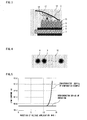
- FIG. 2 is a cross-sectional view showing the structure of a portion (shown by a circle marked by the numeral 13) of the semiconductor device of FIG. 1 near guard rings 14 of one of semiconductor chips 8
- FIG. 3 is a cross-sectional view showing as a comparative example the structure of a portion of a semiconductor device near guard rings 14 of one of semiconductor chips 8 in which a wire 3 is not fitted with a low electrification covering 9
- FIG. 4 is a cross-sectional view showing a principal part of the semiconductor device according to the first embodiment shown in FIG. 1, FIG.
- FIG. 5 is a diagram showing a comparison of time durations until leak currents begin to flow in the semiconductor device of the first embodiment and in the comparative example
- FIG. 6 is a diagram showing how easily a space charge is produced with a sealing material and a low electrification material
- FIG. 7 is a diagram showing a comparison of leak currents (average values) which flow in the semiconductor device of the first embodiment and that of the comparative example.
- the semiconductor device includes a base plate 4, an insulator substrate 6 disposed on the base plate 4, the insulator substrate 6 having an upper electrode 5 and a lower electrode 7 which is joined to the base plate 4 by soldering, for instance, a plurality of semiconductor chips 8, such as IGBTs or diodes which are disposed on the insulator substrate 6, the semiconductor chips 8 being joined to the upper electrode 5 by soldering, for instance, a plurality of external terminals 1 for establishing external electrical connections of the semiconductor device, a plurality of wires 3 for establishing electrical connections between the semiconductor chips 8 and the external terminals 1, between one semiconductor chip 8 and another and between the external terminals 1 and the upper electrode 5, and a case 2 accommodating individual elements of the semiconductor device, where the "individual elements" include the external terminals 1, the insulator substrate 6, the upper electrode 5, the lower electrode 7, the base plate 4 and the wires 3.
- soldering for instance, a plurality of semiconductor chips 8, such as IGBTs or diodes which are disposed on the insulator substrate 6, the semiconductor
- a sealing material 12 like silicone gel is filled in the case 2 of which top side is closed by a protective resin cover 11 made of epoxy resin, for instance, and a lid 10 for protecting an upper part of the sealing material 12.
- a protective resin cover 11 made of epoxy resin, for instance
- a lid 10 for protecting an upper part of the sealing material 12.
- part of each wire 3 is wrapped by an insulative low electrification covering 9 which produces a lesser electric charge buildup than the sealing material 12.
- guard rings 14 on each semiconductor chip 8 for reducing an electric field formed thereon. While each wire bonding area is surrounded by four guard rings 14 as depicted in FIG. 2 in the semiconductor device of the first embodiment, the number of guard rings 14 is actually determined as appropriate depending on the type of each semiconductor chip 8. As can be seen from FIG.
- the low electrification covering 9 is fitted only on that part of each wire 3 which is located immediately above the guard rings 14, wherein the low electrification covering 9 is made of such a low electrification material as silicone rubber, high-rigidity gel or polyimide resin which contains a low concentration (preferably 1 ppm or less) of ionic substances (e.g., Na + , K + , Cl - ). Practically, a few wires 3 run immediately above the guard rings 14 in most cases. In this embodiment, the low electrification covering 9 is fitted around each wire 3 as shown in FIG. 4 in actuality.
- the low electrification covering 9 may be formed by applying the low electrification material directly to each wire 3 or by fitting a heat-shrink tube made of an appropriate low electrification material on each wire 3 and causing the tube to shrink by application of heat.
- the semiconductor device of the first embodiment thus structured can suppress such phenomena as a buildup of electric charge 17 on a surface area of the guard rings 14 where an intense electric field is formed and conventionally experienced injection of the electric charge 17 from the wires 3 into the sealing material 12 (see FIG. 3) due to increased wire insulating properties achieved by the low electrification coverings 9 (see FIG. 2).
- Shown in FIG. 6 is an example of how much the electric charge can develop in the sealing material (gel) 12 and in the low electrification material (rubber) used for forming the low electrification coverings 9. It is apparent from FIG. 6 that the electric charge does not build up so much in the low electrification material of the low electrification coverings 9 as in the sealing material 12 even when subjected to an intense electric field. This obviously proves an advantage of the low electrification coverings 9.
- the semiconductor device of the first embodiment can suppress the leak current to approximately 1/100th of the leak current flowing in the semiconductor device of the comparative example (FIG. 3) of which wires 3 are not covered or coated with any anti-electric charge material. It follows that the above-described structure of the embodiment helps achieve more reliable insulating performance. Furthermore, it can be seen from FIG. 5 that the leak current flowing in the semiconductor device of the comparative example rises much earlier than in the semiconductor device of the first embodiment. This also proves that the structure of the embodiment obviously provides improved insulating performance.
- the low electrification covering 9 is fitted only on that part of each wire 3 which is located immediately above the guard rings 14 and, thus, another part of each wire 3 marked by a circle A in FIG. 2 where each wire 3 is bonded to an emitter 15 located on an upper surface of each semiconductor chip 8 is not provided with the low electrification covering 9.
- This structure ensures that the part of each wire 3 to be bonded marked by the circle A will not break as a result of heat shrinkage of the low electrification covering 9 occurring in a high-temperature cycle even though the low electrification covering 9 is made of a material harder than the sealing material (gel) 12. This serves to improve mechanical reliability of the semiconductor device.
- the above-described structure of the first embodiment makes it possible to manufacture a semiconductor device in which a low electrification covering fitted on part of each wire located close to guard rings substantially restricts injection of electric charge from wires into a sealing material and suppresses an increase in leak current caused by the injected electric charge, thereby providing a high dielectric withstand voltage and high reliability to prevent switching errors and breakdown due to overcurrent of a semiconductor chip.
- This structure also makes it possible to efficiently manufacture a highly reliable semiconductor device at low cost because the low electrification covering need not be fitted all along each wire, thus reducing the amount of the low electrification material to be used and time required for fitting the low electrification covering.
- a power module having a high dielectric withstand voltage and high reliability in which a layer of low electrification material containing silicone rubber, high-rigidity gel or polyimide resin as a primary constituent is disposed above guard rings so that an electric charge injected from wires through a sealing material is entrapped by the low electrification material without affecting the guard rings and the leak current is suppressed.
- the structure of the present embodiment employing the low electrification covering fitted on each wire substantially suppresses injection of the electric charge from wires into the sealing material that is a major source of the leak current, so that the leak current can be suppressed in an efficient manner.
- the foregoing first embodiment shows an example in which the low electrification covering is fitted on that part of each wire which is located immediately above (or in the vicinity of) the guard rings 14, an area where the low electrification covering is fitted may exceed the width of the guard rings, yet providing the same advantageous effect as thus far discussed, if the low electrification material covers at least that part of each wire which is located immediately above the guard rings 14. Also, an increase in the leak current is related to the injection of the electric charge in a direction toward an upper part of each guard ring and, therefore, the aforementioned effect of suppressing the leak current is achieved if only approximately a semicylindrical part of each wire facing the guard rings is covered by the low electrification material.
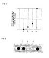
- FIG. 8 is a diagram showing a comparison of a work function of aluminum and work functions of metallic materials which may be used in producing a semiconductor device according to a second embodiment of the invention.
- the semiconductor device of the second embodiment is characterized in that each wire 3 made of aluminum is plated with such a metal as nickel, gold or platinum having a higher work function than aluminum as shown in FIG. 8 so that a coating of such a metal is disposed around an outer surface of each wire 3.
- the work function represents the amount of energy required to remove an electric charge (electron) from a potential barrier of the surface of a solid medium into field-free space, so that the higher the work function of a metallic material, the more reduced is ejection of electrons from the material.
- the wires 3 are coated with a metallic material having a high work function so that each wire 3 connected to an emitter 15 of each semiconductor chip 8 works as a negative electrode. Since the metallic material having a high work function restricts injection of a negative electric charge, the wires 3 plated with the metallic material having the high work function serve to restrict injection of the negative electric charge into a sealing material and suppress an increase in leak current caused by the injected electric charge, thereby providing a high dielectric withstand voltage and high reliability to prevent switching errors and breakdown due to overcurrent of a semiconductor chip.
- the metallic material having the high work function is plated only on that part of each wire which is located immediately above guard rings, it is possible to improve mechanical reliability of the semiconductor device especially at a joint between each wire and an electrode. Furthermore, since the metallic material having the high work function need not be plated all along each wire, the above-described structure of the second embodiment provides the same advantageous effect as the first embodiment, such as a reduction in manufacturing cost.
- the bare wires 3 are made of aluminum in the semiconductor device of the second embodiment, the invention is not limited thereto.
- the entirety of the wires 3 may be made of a metallic material, such as nickel, gold or platinum, having a higher work function than aluminum.
- This variation of the second embodiment provides the same advantageous effect as the second embodiment. Additionally, this variation eliminates the need for a process of plating the wires 3, making it possible to efficiently manufacture a highly reliable semiconductor device with reduced manufacturing time and at low cost.
- each semiconductor chip 8 is plated with a metallic material having a higher work function than aluminum, it would be possible to reduce the amount of electric charge released from each semiconductor chip 8, making it possible to further suppress the leak current and manufacture a yet more reliable semiconductor device.
- the invention is not limited to these structures.
- the wires 3 may be covered by both the low electrification material and the plated layer of the metallic material having a high work function.
- the individual wires 3 are covered by the low electrification material or the plated layer of the metallic material having a high work function only in the vicinity of the guard rings 14 in the aforementioned embodiments, the invention is not limited thereto.
- the low electrification covering 9 made of the low electrification material, the plated layer of the metallic material having a high work function, or both may be provided all along each wire 3 to achieve the same advantageous effect with respect to leak current suppression.
- the invention is not limited to these structures.
- two or more wires 3 may be wrapped together by means of a strip of tape 18 made of or containing a low electrification material or a metallic material having a high work function as illustrated in FIG. 9 which is a cross-sectional view showing a principal part of a semiconductor device according to a third embodiment of the invention.
- This structure helps reduce the amount of labor required for handling the individual wires 3, yet providing the same advantageous effect as discussed in the first and second embodiments.
- the structure of the third embodiment produces the effect of restricting injection of the electric charge from the wires 3 into the sealing material and makes it possible to efficiently manufacture a highly reliable semiconductor device having a high withstand voltage.
- wires 3 are used for establishing electrical connections in the semiconductor devices of the foregoing embodiments
- means for establishing electrical connections is not limited to the wires 3.
- the invention is applicable to a semiconductor device employing ball electrodes having a ball-shaped electrode surface covered by a low electrification material or plated with a metallic material having a high work function, or employing ball electrodes made of a metallic material having a high work function, as means for establishing electrical connections.
- the invention is also applicable to a semiconductor device employing an interposer, a printed circuit board or direct leads for wire-free connection of each chip and external terminals as means for establishing electrical connections. Needless to say, the invention confers the same advantageous effect as discussed above with reference to the foregoing embodiments.
- the invention has been explained with reference to the semiconductor devices employing a case-and-lid type encapsulation technique, the invention is similarly applicable to semiconductor devices manufactured by other techniques, such as transfer mold process, still producing the same advantageous effect.
- the invention is also applicable to semiconductor devices provided with a built-in heat sink or a separate heat sink, as well as to semiconductor devices incorporating silicon chips, SiC chips, diodes, other types of transistors than IGBTs and/or integrated circuits (ICs), for instance, yet producing the same advantageous effect.
- the invention is applicable with the same advantageous effect to various types of semiconductor devices, such as a junction type in which electrodes are electrically connected to a base plate and semiconductor chips by fused metal joining like soldering, a mechanical contact type in which electrodes are electrically connected to a base plate and semiconductor chips by application of mechanical pressure exerted inward from outside the electrodes by means an elastic member or bolting, and a junction and mechanical contact combination type.
- semiconductor devices such as a junction type in which electrodes are electrically connected to a base plate and semiconductor chips by fused metal joining like soldering, a mechanical contact type in which electrodes are electrically connected to a base plate and semiconductor chips by application of mechanical pressure exerted inward from outside the electrodes by means an elastic member or bolting, and a junction and mechanical contact combination type.
Landscapes
- Structures Or Materials For Encapsulating Or Coating Semiconductor Devices Or Solid State Devices (AREA)
- Wire Bonding (AREA)
Abstract
Description
- The present invention relates to a semiconductor device in which injection of electric charge from an electric charge source is restricted to provide highly reliable insulating performance.
- There is a growing demand today for a power module suited for reliably controlling a large current flowing in such electric apparatuses as motors and heaters. One requirement in the design of this kind of power module is to structure the same to provide a high withstand voltage retaining capability so that a leak current which may flow other than through an ordinary current path will not flow between a collector (positive electrode) and an emitter (negative electrode) to which an extremely high voltage is applied, for instance. A structure having such a high withstand voltage retaining capability is obtained by use of a power semiconductor chip like an insulated-gate bipolar transistor (IGBT) and insulative sealing resin for packaging the power semiconductor chip, for example. One conventionally known example of a structure having a high withstand voltage retaining capability is a guard ring structure which typically includes a plurality of guard rings separated from one another running along an outer peripheral region of an upper surface of a semiconductor chip and a plurality of capacitive elements made of an insulating material like sealing resin filled between the adjacent guard rings. The guard ring structure thus formed reduces an electric field produced along the surface of the semiconductor chip and suppresses the leak current. The guard ring structure formed in the outer peripheral region of the semiconductor chip serves to provide an increased dielectric withstand voltage in surface directions between an emitter located in a central region of the upper surface of the semiconductor chip and a collector located below the emitter.
- On the other hand,
Japanese Patent Application Publication No. 1995-30015 - Generally, a leak current increases in a conventional semiconductor device even under room temperature conditions when a high voltage is applied across an emitter and a collector and this may develop a device failure like incorrect switching and breakdown due to overcurrent of a semiconductor chip, such an IGBT chip or a diode chip. This kind of leak current is supposed to increase when a negative charge accumulates in a guard ring due to a strong electric field produced between a conductive wire electrically connected to the emitter and the guard ring, resulting in excessive formation of a depletion layer in a multilayer structure of the semiconductor device and allowing the leak current to flow through the depletion layer. Another problem of the conventional semiconductor device is that if a wire which is a source of electric charge is located immediately above a guard ring where the electric field is maximized, the wire continuously supplies the electric charge and the amount of electric charge injected into sealing material increases with time, which could cause an increase in the leak current and eventual malfunctioning of a semiconductor chip. In a case where a silicon carbide (SiC) chip having a higher operating temperature is used instead of a silicon chip, for instance, the electric charge can more easily be injected into sealing material. This also develops a problem that malfunctioning of the semiconductor chip can occur due to an increase in the leak current.
- In light of the aforementioned problems of the prior art, it is an object of the invention to provide a semiconductor device featuring highly reliable insulating performance by restricting injection of electric charge from an electric charge source that can cause an increase in leak current.
- According to the invention, a semiconductor device includes an insulator substrate mounted on a base plate, the insulator substrate having an electrode, a semiconductor chip mounted on the insulator substrate, external terminals for establishing external electrical connections of the semiconductor device, means for establishing electrical connections among the external terminals, the electrode and the semiconductor chip, a case accommodating the insulator substrate, the semiconductor chip, the external terminals and the means for establishing electrical connections which are sealed by a sealing material filled in the case, a lid for protecting an upper part of the sealing material, and an insulative low electrification material covering the means for establishing electrical connections, the low electrification material having a lesser tendency to produce an electric charge buildup than the sealing material.
- In the semiconductor device thus structured, the low electrification material fitted on the means (wires) for establishing electrical connections serves to substantially restrict injection of electric charge from the wires into the sealing material and suppress an increase in leak current caused by the injected electric charge.
- The foregoing and other objects, features, aspects and advantages of the present invention will become more apparent from the following detailed description when read in conjunction with the accompanying drawings.
-
- FIG. 1 is a cross-sectional view generally showing the structure of a semiconductor device according to a first embodiment of the invention;
- FIG. 2 is a cross-sectional view showing the structure of a portion (shown by a circle marked by the numeral 13) of the semiconductor device of FIG. 1 near guard rings of one of semiconductor chips;
- FIG. 3 is a cross-sectional view showing as a comparative example the structure of a portion of a semiconductor device near guard rings of one of semiconductor chips in which a wire is not fitted with a low electrification covering;
- FIG. 4 is a cross-sectional view showing a principal part of the semiconductor device according to the first embodiment shown in FIG. 1;
- FIG. 5 is a diagram showing a comparison of time durations until leak currents begin to flow in the semiconductor device of the first embodiment and in the comparative example;
- FIG. 6 is a diagram showing how easily a space charge is produced with a sealing material and a low electrification material;
- FIG. 7 is a diagram showing a comparison of leak currents (average values) which flow in the semiconductor device of the first embodiment and that of the comparative example;
- FIG. 8 is a diagram showing a comparison of a work function of aluminum and work functions of metallic materials which may be used in producing a semiconductor device according to a second embodiment of the invention; and
- FIG. 9 is a cross-sectional view showing a principal part of a semiconductor device according to a third embodiment of the invention.
- The invention is now described in detail with reference to preferred embodiments thereof which are illustrated in the accompanying drawings.
- FIG. 1 is a cross-sectional view generally showing the structure of a semiconductor device according to a first embodiment of the invention, FIG. 2 is a cross-sectional view showing the structure of a portion (shown by a circle marked by the numeral 13) of the semiconductor device of FIG. 1
near guard rings 14 of one ofsemiconductor chips 8, FIG. 3 is a cross-sectional view showing as a comparative example the structure of a portion of a semiconductor device nearguard rings 14 of one ofsemiconductor chips 8 in which awire 3 is not fitted with a low electrification covering 9, FIG. 4 is a cross-sectional view showing a principal part of the semiconductor device according to the first embodiment shown in FIG. 1, FIG. 5 is a diagram showing a comparison of time durations until leak currents begin to flow in the semiconductor device of the first embodiment and in the comparative example, FIG. 6 is a diagram showing how easily a space charge is produced with a sealing material and a low electrification material, and FIG. 7 is a diagram showing a comparison of leak currents (average values) which flow in the semiconductor device of the first embodiment and that of the comparative example. - Referring to FIG. 1, the semiconductor device includes a
base plate 4, aninsulator substrate 6 disposed on thebase plate 4, theinsulator substrate 6 having anupper electrode 5 and alower electrode 7 which is joined to thebase plate 4 by soldering, for instance, a plurality ofsemiconductor chips 8, such as IGBTs or diodes which are disposed on theinsulator substrate 6, thesemiconductor chips 8 being joined to theupper electrode 5 by soldering, for instance, a plurality ofexternal terminals 1 for establishing external electrical connections of the semiconductor device, a plurality ofwires 3 for establishing electrical connections between thesemiconductor chips 8 and theexternal terminals 1, between onesemiconductor chip 8 and another and between theexternal terminals 1 and theupper electrode 5, and acase 2 accommodating individual elements of the semiconductor device, where the "individual elements" include theexternal terminals 1, theinsulator substrate 6, theupper electrode 5, thelower electrode 7, thebase plate 4 and thewires 3. To encapsulate these elements, asealing material 12 like silicone gel is filled in thecase 2 of which top side is closed by aprotective resin cover 11 made of epoxy resin, for instance, and alid 10 for protecting an upper part of the sealingmaterial 12. As depicted in FIG. 2, part of eachwire 3 is wrapped by an insulative low electrification covering 9 which produces a lesser electric charge buildup than the sealingmaterial 12. - Given below is a detailed description of how the low electrification covering 9 is provided. There are provided
guard rings 14 on eachsemiconductor chip 8 for reducing an electric field formed thereon. While each wire bonding area is surrounded by fourguard rings 14 as depicted in FIG. 2 in the semiconductor device of the first embodiment, the number ofguard rings 14 is actually determined as appropriate depending on the type of eachsemiconductor chip 8. As can be seen from FIG. 2, the low electrification covering 9 is fitted only on that part of eachwire 3 which is located immediately above theguard rings 14, wherein the low electrification covering 9 is made of such a low electrification material as silicone rubber, high-rigidity gel or polyimide resin which contains a low concentration (preferably 1 ppm or less) of ionic substances (e.g., Na+, K+, Cl-). Practically, afew wires 3 run immediately above the guard rings 14 in most cases. In this embodiment, the low electrification covering 9 is fitted around eachwire 3 as shown in FIG. 4 in actuality. The low electrification covering 9 may be formed by applying the low electrification material directly to eachwire 3 or by fitting a heat-shrink tube made of an appropriate low electrification material on eachwire 3 and causing the tube to shrink by application of heat. - The semiconductor device of the first embodiment thus structured can suppress such phenomena as a buildup of
electric charge 17 on a surface area of theguard rings 14 where an intense electric field is formed and conventionally experienced injection of theelectric charge 17 from thewires 3 into the sealing material 12 (see FIG. 3) due to increased wire insulating properties achieved by the low electrification coverings 9 (see FIG. 2). Shown in FIG. 6 is an example of how much the electric charge can develop in the sealing material (gel) 12 and in the low electrification material (rubber) used for forming thelow electrification coverings 9. It is apparent from FIG. 6 that the electric charge does not build up so much in the low electrification material of the low electrification coverings 9 as in the sealingmaterial 12 even when subjected to an intense electric field. This obviously proves an advantage of thelow electrification coverings 9. - Also, as indicated by actual measurements of the leak currents shown in FIG. 7, the semiconductor device of the first embodiment (FIG. 2) can suppress the leak current to approximately 1/100th of the leak current flowing in the semiconductor device of the comparative example (FIG. 3) of which
wires 3 are not covered or coated with any anti-electric charge material. It follows that the above-described structure of the embodiment helps achieve more reliable insulating performance. Furthermore, it can be seen from FIG. 5 that the leak current flowing in the semiconductor device of the comparative example rises much earlier than in the semiconductor device of the first embodiment. This also proves that the structure of the embodiment obviously provides improved insulating performance. - In this embodiment, the low electrification covering 9 is fitted only on that part of each
wire 3 which is located immediately above theguard rings 14 and, thus, another part of eachwire 3 marked by a circle A in FIG. 2 where eachwire 3 is bonded to anemitter 15 located on an upper surface of eachsemiconductor chip 8 is not provided with the low electrification covering 9. This structure ensures that the part of eachwire 3 to be bonded marked by the circle A will not break as a result of heat shrinkage of the low electrification covering 9 occurring in a high-temperature cycle even though the low electrification covering 9 is made of a material harder than the sealing material (gel) 12. This serves to improve mechanical reliability of the semiconductor device. - The above-described structure of the first embodiment makes it possible to manufacture a semiconductor device in which a low electrification covering fitted on part of each wire located close to guard rings substantially restricts injection of electric charge from wires into a sealing material and suppresses an increase in leak current caused by the injected electric charge, thereby providing a high dielectric withstand voltage and high reliability to prevent switching errors and breakdown due to overcurrent of a semiconductor chip. This structure also makes it possible to efficiently manufacture a highly reliable semiconductor device at low cost because the low electrification covering need not be fitted all along each wire, thus reducing the amount of the low electrification material to be used and time required for fitting the low electrification covering.
- It might be possible to structure a power module having a high dielectric withstand voltage and high reliability in which a layer of low electrification material containing silicone rubber, high-rigidity gel or polyimide resin as a primary constituent is disposed above guard rings so that an electric charge injected from wires through a sealing material is entrapped by the low electrification material without affecting the guard rings and the leak current is suppressed. However, it is needless to say that the structure of the present embodiment employing the low electrification covering fitted on each wire substantially suppresses injection of the electric charge from wires into the sealing material that is a major source of the leak current, so that the leak current can be suppressed in an efficient manner.
- While the foregoing first embodiment shows an example in which the low electrification covering is fitted on that part of each wire which is located immediately above (or in the vicinity of) the
guard rings 14, an area where the low electrification covering is fitted may exceed the width of the guard rings, yet providing the same advantageous effect as thus far discussed, if the low electrification material covers at least that part of each wire which is located immediately above theguard rings 14. Also, an increase in the leak current is related to the injection of the electric charge in a direction toward an upper part of each guard ring and, therefore, the aforementioned effect of suppressing the leak current is achieved if only approximately a semicylindrical part of each wire facing the guard rings is covered by the low electrification material. Furthermore, it is possible to increase the reliability of the semiconductor device in a high-temperature operating region by using insulative heat-resistant silicone rubber or heat-resistant resin which produces a lesser electric charge buildup than the sealing material in the low electrification coverings taking into consideration a temperature increase of the semiconductor device. - Generally, aluminum is often used as a material of
wires 3 in the manufacture of semiconductor devices for various reasons, such as relatively low cost and ease of manufacturing. FIG. 8 is a diagram showing a comparison of a work function of aluminum and work functions of metallic materials which may be used in producing a semiconductor device according to a second embodiment of the invention. Unlike the semiconductor device of the first embodiment employing thelow electrification coverings 9, the semiconductor device of the second embodiment is characterized in that eachwire 3 made of aluminum is plated with such a metal as nickel, gold or platinum having a higher work function than aluminum as shown in FIG. 8 so that a coating of such a metal is disposed around an outer surface of eachwire 3. The work function represents the amount of energy required to remove an electric charge (electron) from a potential barrier of the surface of a solid medium into field-free space, so that the higher the work function of a metallic material, the more reduced is ejection of electrons from the material. - In the semiconductor device of the second embodiment thus structured, the
wires 3 are coated with a metallic material having a high work function so that eachwire 3 connected to anemitter 15 of eachsemiconductor chip 8 works as a negative electrode. Since the metallic material having a high work function restricts injection of a negative electric charge, thewires 3 plated with the metallic material having the high work function serve to restrict injection of the negative electric charge into a sealing material and suppress an increase in leak current caused by the injected electric charge, thereby providing a high dielectric withstand voltage and high reliability to prevent switching errors and breakdown due to overcurrent of a semiconductor chip. - If the metallic material having the high work function is plated only on that part of each wire which is located immediately above guard rings, it is possible to improve mechanical reliability of the semiconductor device especially at a joint between each wire and an electrode. Furthermore, since the metallic material having the high work function need not be plated all along each wire, the above-described structure of the second embodiment provides the same advantageous effect as the first embodiment, such as a reduction in manufacturing cost.
- While the
bare wires 3 are made of aluminum in the semiconductor device of the second embodiment, the invention is not limited thereto. For example, instead of plating thealuminum wires 3, the entirety of thewires 3 may be made of a metallic material, such as nickel, gold or platinum, having a higher work function than aluminum. This variation of the second embodiment provides the same advantageous effect as the second embodiment. Additionally, this variation eliminates the need for a process of plating thewires 3, making it possible to efficiently manufacture a highly reliable semiconductor device with reduced manufacturing time and at low cost. - Moreover, if a surface of the
emitter 15 formed on eachsemiconductor chip 8 is plated with a metallic material having a higher work function than aluminum, it would be possible to reduce the amount of electric charge released from eachsemiconductor chip 8, making it possible to further suppress the leak current and manufacture a yet more reliable semiconductor device. - While the
individual wires 3 are covered by the low electrification material or a plated layer of the metallic material having a high work function in portions in the vicinity of the guard rings 14 in the above-described first and second embodiments, respectively, the invention is not limited to these structures. For example, thewires 3 may be covered by both the low electrification material and the plated layer of the metallic material having a high work function. Also, while theindividual wires 3 are covered by the low electrification material or the plated layer of the metallic material having a high work function only in the vicinity of the guard rings 14 in the aforementioned embodiments, the invention is not limited thereto. If the cost reduction is not of great importance, the low electrification covering 9 made of the low electrification material, the plated layer of the metallic material having a high work function, or both may be provided all along eachwire 3 to achieve the same advantageous effect with respect to leak current suppression. - While the
individual wires 3 are separately covered by at least the low electrification material or the plated layer of the metallic material having a high work function in the foregoing embodiments, the invention is not limited to these structures. For example, two ormore wires 3 may be wrapped together by means of a strip oftape 18 made of or containing a low electrification material or a metallic material having a high work function as illustrated in FIG. 9 which is a cross-sectional view showing a principal part of a semiconductor device according to a third embodiment of the invention. This structure helps reduce the amount of labor required for handling theindividual wires 3, yet providing the same advantageous effect as discussed in the first and second embodiments. Specifically, like the structures of the foregoing embodiments, the structure of the third embodiment produces the effect of restricting injection of the electric charge from thewires 3 into the sealing material and makes it possible to efficiently manufacture a highly reliable semiconductor device having a high withstand voltage. - While the
wires 3 are used for establishing electrical connections in the semiconductor devices of the foregoing embodiments, means for establishing electrical connections is not limited to thewires 3. For example, the invention is applicable to a semiconductor device employing ball electrodes having a ball-shaped electrode surface covered by a low electrification material or plated with a metallic material having a high work function, or employing ball electrodes made of a metallic material having a high work function, as means for establishing electrical connections. The invention is also applicable to a semiconductor device employing an interposer, a printed circuit board or direct leads for wire-free connection of each chip and external terminals as means for establishing electrical connections. Needless to say, the invention confers the same advantageous effect as discussed above with reference to the foregoing embodiments. - Although the invention has been explained with reference to the semiconductor devices employing a case-and-lid type encapsulation technique, the invention is similarly applicable to semiconductor devices manufactured by other techniques, such as transfer mold process, still producing the same advantageous effect. The invention is also applicable to semiconductor devices provided with a built-in heat sink or a separate heat sink, as well as to semiconductor devices incorporating silicon chips, SiC chips, diodes, other types of transistors than IGBTs and/or integrated circuits (ICs), for instance, yet producing the same advantageous effect.
- Furthermore, the invention is applicable with the same advantageous effect to various types of semiconductor devices, such as a junction type in which electrodes are electrically connected to a base plate and semiconductor chips by fused metal joining like soldering, a mechanical contact type in which electrodes are electrically connected to a base plate and semiconductor chips by application of mechanical pressure exerted inward from outside the electrodes by means an elastic member or bolting, and a junction and mechanical contact combination type.
- Various modifications and alterations of this invention will be apparent to those skilled in the art without departing from the scope and spirit of this invention, and it should be understood that this is not limited to the illustrative embodiments set forth herein.
Claims (6)
- A semiconductor device comprising:an insulator substrate mounted on a base plate, said insulator substrate having an electrode;a semiconductor chip mounted on said insulator substrate;external terminals for establishing external electrical connections of said semiconductor device;means for establishing electrical connections among said external terminals, said electrode and said semiconductor chip;a case accommodating said insulator substrate, said semiconductor chip, said external terminals and said means for establishing electrical connections which are sealed by a sealing material filled in said case;a lid for protecting an upper part of said sealing material; andan insulative low electrification material covering said means for establishing electrical connections, said low electrification material having a lesser tendency to produce an electric charge buildup than said sealing material.
- The semiconductor device according to claim 1, wherein a guard ring is formed on said semiconductor chip and said low electrification material covers only that part of said means for establishing electrical connections which is located in the vicinity of said guard ring.
- The semiconductor device according to claim 1, wherein said low electrification material is formed into a tape which surrounds more than one of said means for establishing electrical connections.
- A semiconductor device comprising:an insulator substrate mounted on a base plate, said insulator substrate having an electrode;a semiconductor chip mounted on said insulator substrate;external terminals for establishing external electrical connections of said semiconductor device;means for establishing electrical connections among said external terminals, said electrode and said semiconductor chip;a case accommodating said insulator substrate, said semiconductor chip, said external terminals and said means for establishing electrical connections which are sealed by a sealing material filled in said case;a lid for protecting an upper part of said sealing material; anda metallic material covering said means for establishing electrical connections, said metallic material having a work function higher than that of said means for establishing electrical connections.
- The semiconductor device according to claim 4, wherein a guard ring is formed on said semiconductor chip and said metallic material covers only that part of said means for establishing electrical connections which is located in the vicinity of said guard ring.
- The semiconductor device according to claim 4, wherein said metallic material is formed into a tape which surrounds more than one of said means for establishing electrical connections.
Applications Claiming Priority (1)
| Application Number | Priority Date | Filing Date | Title |
|---|---|---|---|
| JP2006132114A JP4884830B2 (en) | 2006-05-11 | 2006-05-11 | Semiconductor device |
Publications (2)
| Publication Number | Publication Date |
|---|---|
| EP1860697A2 true EP1860697A2 (en) | 2007-11-28 |
| EP1860697A3 EP1860697A3 (en) | 2017-09-13 |
Family
ID=38578564
Family Applications (1)
| Application Number | Title | Priority Date | Filing Date |
|---|---|---|---|
| EP07008986.7A Withdrawn EP1860697A3 (en) | 2006-05-11 | 2007-05-03 | Semiconductor device |
Country Status (3)
| Country | Link |
|---|---|
| US (1) | US7868436B2 (en) |
| EP (1) | EP1860697A3 (en) |
| JP (1) | JP4884830B2 (en) |
Families Citing this family (17)
| Publication number | Priority date | Publication date | Assignee | Title |
|---|---|---|---|---|
| US8410600B2 (en) * | 2009-10-02 | 2013-04-02 | Arkansas Power Electronics International, Inc. | Semiconductor device with protecting film and method of fabricating the semiconductor device with protecting film |
| JP5268994B2 (en) * | 2010-05-31 | 2013-08-21 | 三菱電機株式会社 | Semiconductor module and manufacturing method thereof |
| EP2765601B1 (en) * | 2011-09-30 | 2020-05-06 | Fuji Electric Co., Ltd. | Semiconductor device and method of manufacture thereof |
| DE102012213916A1 (en) * | 2011-11-08 | 2013-05-08 | Robert Bosch Gmbh | Electronic module for a control unit |
| DE102011089474A1 (en) * | 2011-12-21 | 2013-06-27 | Robert Bosch Gmbh | Electronic module for a vehicle |
| WO2013111276A1 (en) * | 2012-01-25 | 2013-08-01 | 三菱電機株式会社 | Power semiconductor device |
| JP5859906B2 (en) * | 2012-04-20 | 2016-02-16 | 三菱電機株式会社 | Semiconductor device and manufacturing method of semiconductor device |
| JP5930070B2 (en) * | 2012-12-28 | 2016-06-08 | 富士電機株式会社 | Semiconductor device |
| US9478473B2 (en) * | 2013-05-21 | 2016-10-25 | Globalfoundries Inc. | Fabricating a microelectronics lid using sol-gel processing |
| US20150001700A1 (en) * | 2013-06-28 | 2015-01-01 | Infineon Technologies Ag | Power Modules with Parylene Coating |
| CN110024118A (en) * | 2016-11-25 | 2019-07-16 | 三菱电机株式会社 | semiconductor device |
| US10177057B2 (en) | 2016-12-15 | 2019-01-08 | Infineon Technologies Ag | Power semiconductor modules with protective coating |
| JP6395173B1 (en) * | 2017-03-29 | 2018-09-26 | 三菱電機株式会社 | Power semiconductor module |
| WO2018179573A1 (en) * | 2017-03-29 | 2018-10-04 | 三菱電機株式会社 | Power semiconductor module |
| JP6826665B2 (en) * | 2018-12-27 | 2021-02-03 | 三菱電機株式会社 | Semiconductor devices, manufacturing methods for semiconductor devices, and power conversion devices |
| JP7647253B2 (en) * | 2021-04-01 | 2025-03-18 | 富士電機株式会社 | Semiconductor module and method for manufacturing the same |
| JP7784974B2 (en) * | 2022-09-08 | 2025-12-12 | 三菱電機株式会社 | Semiconductor device manufacturing method |
Family Cites Families (18)
| Publication number | Priority date | Publication date | Assignee | Title |
|---|---|---|---|---|
| JPS6333831A (en) * | 1986-07-29 | 1988-02-13 | Hitachi Ltd | Bonding wire and wire bonding method |
| JPS6367749A (en) * | 1986-09-09 | 1988-03-26 | Fujitsu Ltd | Semiconductor device |
| JP2701045B2 (en) * | 1988-07-15 | 1998-01-21 | 東レ・ダウコーニング・シリコーン株式会社 | Resin-sealed semiconductor device and method of manufacturing the same |
| JPH03165044A (en) * | 1989-11-22 | 1991-07-17 | Tanaka Denshi Kogyo Kk | Covered wire |
| JPH05218454A (en) * | 1992-01-20 | 1993-08-27 | Nec Corp | Semiconductor device |
| JPH0730015A (en) * | 1993-07-14 | 1995-01-31 | Hitachi Ltd | Semiconductor module and manufacturing method thereof |
| JPH10173101A (en) * | 1996-12-10 | 1998-06-26 | Toshiba Corp | Semiconductor device |
| US6084297A (en) * | 1998-09-03 | 2000-07-04 | Micron Technology, Inc. | Cavity ball grid array apparatus |
| JP3612226B2 (en) * | 1998-12-21 | 2005-01-19 | 株式会社東芝 | Semiconductor device and semiconductor module |
| JP2002076190A (en) * | 2000-08-24 | 2002-03-15 | Toshiba Corp | Circuit board, semiconductor device, and manufacturing method thereof |
| JP3923716B2 (en) * | 2000-09-29 | 2007-06-06 | 株式会社東芝 | Semiconductor device |
| US6670214B1 (en) * | 2000-10-12 | 2003-12-30 | Lsi Logic Corporation | Insulated bonding wire for microelectronic packaging |
| KR100535062B1 (en) * | 2001-06-04 | 2005-12-07 | 마츠시타 덴끼 산교 가부시키가이샤 | High-voltage semiconductor device |
| US6882546B2 (en) * | 2001-10-03 | 2005-04-19 | Formfactor, Inc. | Multiple die interconnect system |
| JP3813098B2 (en) * | 2002-02-14 | 2006-08-23 | 三菱電機株式会社 | Power semiconductor module |
| US6982482B2 (en) * | 2004-02-24 | 2006-01-03 | Applied Pulsed Power, Inc. | Packaging of solid state devices |
| JP2004228593A (en) * | 2004-03-22 | 2004-08-12 | Toshiba Corp | Semiconductor device |
| JP4824318B2 (en) | 2005-01-20 | 2011-11-30 | 三菱電機株式会社 | Semiconductor device |
-
2006
- 2006-05-11 JP JP2006132114A patent/JP4884830B2/en not_active Expired - Fee Related
-
2007
- 2007-04-30 US US11/742,057 patent/US7868436B2/en not_active Expired - Fee Related
- 2007-05-03 EP EP07008986.7A patent/EP1860697A3/en not_active Withdrawn
Also Published As
| Publication number | Publication date |
|---|---|
| EP1860697A3 (en) | 2017-09-13 |
| US20070284719A1 (en) | 2007-12-13 |
| JP4884830B2 (en) | 2012-02-29 |
| US7868436B2 (en) | 2011-01-11 |
| JP2007305757A (en) | 2007-11-22 |
Similar Documents
| Publication | Publication Date | Title |
|---|---|---|
| US7868436B2 (en) | Semiconductor device | |
| JP5232367B2 (en) | Semiconductor device | |
| US10147707B2 (en) | Semiconductor device | |
| CN105765716B (en) | Power semiconductor modular and composite module | |
| US7449774B1 (en) | Semiconductor power module having an electrically insulating heat sink and method of manufacturing the same | |
| US10959333B2 (en) | Semiconductor device | |
| US9754855B2 (en) | Semiconductor module having an embedded metal heat dissipation plate | |
| US8373197B2 (en) | Circuit device | |
| US11984386B2 (en) | Semiconductor device | |
| US20140167241A1 (en) | Semiconductor device | |
| US10068819B2 (en) | Semiconductor device | |
| JP7158392B2 (en) | power semiconductor module | |
| US12100631B2 (en) | Semiconductor device | |
| US20260060115A1 (en) | Semiconductor device | |
| US20210257269A1 (en) | Semiconductor device | |
| JP7131436B2 (en) | Semiconductor device and its manufacturing method | |
| JP3703978B2 (en) | Semiconductor device | |
| WO2021193338A1 (en) | Semiconductor device | |
| US12334409B2 (en) | Semiconductor module | |
| KR20190085587A (en) | High thermal conductivity semiconductor package | |
| TW202226485A (en) | semiconductor device | |
| JP2904154B2 (en) | Electronic circuit device including semiconductor element | |
| US20240355693A1 (en) | Semiconductor device, semiconductor module, and method for manufacturing semiconductor module | |
| JP6891075B2 (en) | Power semiconductor module | |
| JP2022044158A (en) | Method for manufacturing semiconductor module |
Legal Events
| Date | Code | Title | Description |
|---|---|---|---|
| PUAI | Public reference made under article 153(3) epc to a published international application that has entered the european phase |
Free format text: ORIGINAL CODE: 0009012 |
|
| AK | Designated contracting states |
Kind code of ref document: A2 Designated state(s): AT BE BG CH CY CZ DE DK EE ES FI FR GB GR HU IE IS IT LI LT LU LV MC MT NL PL PT RO SE SI SK TR |
|
| AX | Request for extension of the european patent |
Extension state: AL BA HR MK YU |
|
| RIC1 | Information provided on ipc code assigned before grant |
Ipc: H01L 23/373 20060101ALN20170509BHEP Ipc: H01L 23/58 20060101ALI20170509BHEP Ipc: H01L 29/06 20060101ALN20170509BHEP Ipc: H01L 23/42 20060101ALN20170509BHEP Ipc: H01L 23/13 20060101ALN20170509BHEP Ipc: H01L 23/49 20060101AFI20170509BHEP Ipc: H01L 25/065 20060101ALN20170509BHEP Ipc: H01L 23/60 20060101ALI20170509BHEP Ipc: H01L 23/053 20060101ALN20170509BHEP Ipc: H01L 23/29 20060101ALN20170509BHEP |
|
| PUAL | Search report despatched |
Free format text: ORIGINAL CODE: 0009013 |
|
| AK | Designated contracting states |
Kind code of ref document: A3 Designated state(s): AT BE BG CH CY CZ DE DK EE ES FI FR GB GR HU IE IS IT LI LT LU LV MC MT NL PL PT RO SE SI SK TR |
|
| AX | Request for extension of the european patent |
Extension state: AL BA HR MK RS |
|
| RIC1 | Information provided on ipc code assigned before grant |
Ipc: H01L 29/06 20060101ALN20170809BHEP Ipc: H01L 23/053 20060101ALN20170809BHEP Ipc: H01L 23/60 20060101ALI20170809BHEP Ipc: H01L 23/29 20060101ALN20170809BHEP Ipc: H01L 23/42 20060101ALN20170809BHEP Ipc: H01L 23/58 20060101ALI20170809BHEP Ipc: H01L 23/373 20060101ALN20170809BHEP Ipc: H01L 23/49 20060101AFI20170809BHEP Ipc: H01L 23/13 20060101ALN20170809BHEP Ipc: H01L 25/065 20060101ALN20170809BHEP |
|
| 17P | Request for examination filed |
Effective date: 20171121 |
|
| RBV | Designated contracting states (corrected) |
Designated state(s): AT BE BG CH CY CZ DE DK EE ES FI FR GB GR HU IE IS IT LI LT LU LV MC MT NL PL PT RO SE SI SK TR |
|
| RBV | Designated contracting states (corrected) |
Designated state(s): AT BE BG CH CY CZ DE DK EE ES FI FR GB GR HU IE IS IT LI LT LU LV MC MT NL PL PT RO SE SI SK TR |
|
| AKX | Designation fees paid |
Designated state(s): CH DE GB LI |
|
| AXX | Extension fees paid |
Extension state: HR Extension state: RS Extension state: BA Extension state: MK Extension state: AL |
|
| STAA | Information on the status of an ep patent application or granted ep patent |
Free format text: STATUS: THE APPLICATION HAS BEEN WITHDRAWN |
|
| 18W | Application withdrawn |
Effective date: 20210104 |