EP1860061B1 - Integrated die level stress isolation for a MEMS device - Google Patents
Integrated die level stress isolation for a MEMS device Download PDFInfo
- Publication number
- EP1860061B1 EP1860061B1 EP07108602A EP07108602A EP1860061B1 EP 1860061 B1 EP1860061 B1 EP 1860061B1 EP 07108602 A EP07108602 A EP 07108602A EP 07108602 A EP07108602 A EP 07108602A EP 1860061 B1 EP1860061 B1 EP 1860061B1
- Authority
- EP
- European Patent Office
- Prior art keywords
- base
- support device
- mems
- posts
- cavities
- Prior art date
- Legal status (The legal status is an assumption and is not a legal conclusion. Google has not performed a legal analysis and makes no representation as to the accuracy of the status listed.)
- Ceased
Links
Images



Classifications
-
- B—PERFORMING OPERATIONS; TRANSPORTING
- B81—MICROSTRUCTURAL TECHNOLOGY
- B81B—MICROSTRUCTURAL DEVICES OR SYSTEMS, e.g. MICROMECHANICAL DEVICES
- B81B7/00—Microstructural systems ; Auxiliary parts of microstructural devices or systems
- B81B7/0032—Packages or encapsulation
- B81B7/0045—Packages or encapsulation for reducing stress inside of the package structure
- B81B7/0048—Packages or encapsulation for reducing stress inside of the package structure between the MEMS die and the substrate
Definitions
- Microelectromechanical Systems (MEMS) devices are typically attached to a rigid housing structure, then the rigid housing structure is attached to some other device, such as a circuit board. Small strain forces between the rigid housing structure and the MEMS device detrimentally affect the performance of the MEMS sensor located within the MEMS device. Some of the strain forces are due to differences in co-efficients of thermal expansion between the rigid structure and the MEMS device.
- the present invention provides a Microelectromechanical Systems (MEMS) package.
- the MEMS package includes a housing having a cavity with a base surface located within the cavity and a MEMS device bonded within the cavity.
- the MEMS device includes a MEMS sensor and a base connected to the MEMS sensor at a first surface.
- the base includes a first support device that is collocated with the MEMS sensor and has a first side located adjacent to the entire first surface of the MEMS sensor, and a second support device that is partially physically isolated from the first support device.
- An attachment device connects the second support device to the base surface of the housing wherein a second side of the first support device that is opposite the first side of the first support device is not in contact with the base surface of the housing and wherein the second support device is partially physically isolated from the first support device by one or more cavities.
- the second support device includes a plurality of posts located adjacent to edges of the base.
- the plurality of posts includes four corner posts and four side posts, each of the four corner posts are separated from two of the four side posts by two of the cavities.
- FIGURE 1 illustrates a cross-sectional view of a packaged MEMS device formed in accordance with the prior art
- FIGURE 2A illustrates a cross-sectional view of a packaged MEMS device formed in accordance with an embodiment of the present invention
- FIGURE 2B illustrates a blown-up, perspective view of the packaged MEMS device shown in FIGURE 2A ;
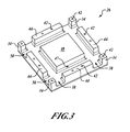
- FIGURE 3 illustrates an inverted perspective view of a MEMS device formed in accordance with an embodiment of the present invention.
- FIGURE 4 illustrates an inverted perspective view of a MEMS device formed in accordance with an alternate embodiment of the present invention.
- a Microelectromechanical System (MEMS) package system 20 as formed in accordance with an embodiment of the present invention is shown.
- the system 20 includes a MEMS device 24 that is located within a housing volume 28 formed by a housing 22 that includes a base portion 22a and a lid 22b.
- the MEMS device 24 includes a MEMS sensor 30 located in a sensor layer that is positioned or attached to a top surface of a substrate or base structure 26. In one embodiment, the sensor 30 is covered by a capping device 32.
- portions of the base structure 26 have been removed prior to attaching the base structure 26 inside the housing 22.
- the cavities 38 and 50 extend from a bottom surface of the structure 26 to a predefined distance vertically within the structure 26.
- the result is four side structures 44 (two of which are shown in FIGURE 2A ) and a center structure 48 ( FIGURE 3 ) that are separated by the cavities 38 and 50.
- Each of the four side structures 44 are attached to a base surface within the housing volume 28 using attachment mechanisms 42 in order to attach the MEMS device 24 to the housing 22.
- attachment mechanisms 42 include gold stud bumps, solder or epoxy.
- the center structure 48 is located under the MEMS sensor 30 that is located in the sensor layer. Thus, any undesired forces between the base structure 26 and the housing 22 are only felt at the side structures 44 with the cavities 38, 50 isolating the center structure 48 and the MEMS sensor 30 from these forces.
- the base structure 26 is shown in perspective view and flipped upside down in order to show all the features formed in accordance with one embodiment.
- the base structure 26 has been etched or machined to include two sets of cavities 38 and 50 that create four corner posts 34, the four side structures 44, and the center structure 48.
- the base structure 26 may be made of a number of different materials, such as silicon or glass, e.g. Pyrex glass.
- a number of different methods can be used in order to remove material of the base structure 26 in order to form two sets of cavities 38 and 50 that isolate the center structure 48 from the corner posts 34 and the side structures 44.
- One example method for removal of the material of the structure 26 to form the cavities 38, 50 is by using a high precision saw.
- Another example method for removal of the material of the substrate 26 uses any of a number of known masking and etching techniques, such as Deep Reactive Ion Etching.
- the longitudinal axis of the cavities 38 are formed at 90° from the longitudinal axis of the cavities 50.
- the angular relationship of the longitudinal axis of the cavities 38, 50 could be formed at any angle.
- the cavities 38, 50 may be curved instead of straight or a combination of geometric shapes.
- the four corner posts 34 and the four side structures 44 are attached to the base surface in the housing volume 28 using the attachment mechanisms 42. Because the center structure 48 is co-located with the MEMS sensor 30 and is isolated from the attachment mechanisms 42, the structural deformations are limited to portions of the device 24 that are external to the center structure 48 and thus external to the MEMS sensor 30.
- FIGURE 4 illustrates a base structure 76 formed in accordance with an alternate embodiment of the present invention.
- the base structure 76 is etched or machined to include a cavity 80.
- the cavity 80 defines a center structure 68 that is surrounded on four sides by the cavity 80.
- the cavity 80 is formed by a circumferential wall 78 that extends around the circumference of the base structure 76.
- the cavity 80 is formed by silicon or glass etching techniques, precision sawing, or other silicon or glass removal techniques depending upon the material composition of the base structure 76.
- the circumferential wall 78 is attached at various points to the base surface of the housing volume 28 in the housing 22 ( FIGURE 2A ) using the attachment mechanisms 42.
- the cavity 80 may be circular in shape or some other shape that still allows for force isolation between the circumferential wall 78 and the center structure 68.
Landscapes
- Engineering & Computer Science (AREA)
- Microelectronics & Electronic Packaging (AREA)
- Computer Hardware Design (AREA)
- Pressure Sensors (AREA)
- Micromachines (AREA)
Description
- Microelectromechanical Systems (MEMS) devices are typically attached to a rigid housing structure, then the rigid housing structure is attached to some other device, such as a circuit board. Small strain forces between the rigid housing structure and the MEMS device detrimentally affect the performance of the MEMS sensor located within the MEMS device. Some of the strain forces are due to differences in co-efficients of thermal expansion between the rigid structure and the MEMS device.
- Therefore, there exists a need for isolation of MEMS devices from certain packaging forces.
- Published patent application
US2004/0046248 A1 discloses plate-like interposers which are mounted along opposite sides of a MEMS die. Said interposers decouple the MEMS die from the package substrate and therefore the MEMS die is less subjected to stresses from the substrate. - The present invention provides a Microelectromechanical Systems (MEMS) package. The MEMS package includes a housing having a cavity with a base surface located within the cavity and a MEMS device bonded within the cavity. The MEMS device includes a MEMS sensor and a base connected to the MEMS sensor at a first surface. The base includes a first support device that is collocated with the MEMS sensor and has a first side located adjacent to the entire first surface of the MEMS sensor, and a second support device that is partially physically isolated from the first support device. An attachment device connects the second support device to the base surface of the housing wherein a second side of the first support device that is opposite the first side of the first support device is not in contact with the base surface of the housing and wherein the second support device is partially physically isolated from the first support device by one or more cavities. The second support device includes a plurality of posts located adjacent to edges of the base. The plurality of posts includes four corner posts and four side posts, each of the four corner posts are separated from two of the four side posts by two of the cavities.
- The preferred and alternative embodiments of the present invention are described in detail below with reference to the following drawings:
-
FIGURE 1 illustrates a cross-sectional view of a packaged MEMS device formed in accordance with the prior art; -
FIGURE 2A illustrates a cross-sectional view of a packaged MEMS device formed in accordance with an embodiment of the present invention; -
FIGURE 2B illustrates a blown-up, perspective view of the packaged MEMS device shown inFIGURE 2A ; -
FIGURE 3 illustrates an inverted perspective view of a MEMS device formed in accordance with an embodiment of the present invention; and -
FIGURE 4 illustrates an inverted perspective view of a MEMS device formed in accordance with an alternate embodiment of the present invention. - As shown in
FIGURES 2A and2B , a Microelectromechanical System (MEMS)package system 20 as formed in accordance with an embodiment of the present invention is shown. Thesystem 20 includes aMEMS device 24 that is located within ahousing volume 28 formed by ahousing 22 that includes abase portion 22a and alid 22b. TheMEMS device 24 includes aMEMS sensor 30 located in a sensor layer that is positioned or attached to a top surface of a substrate orbase structure 26. In one embodiment, thesensor 30 is covered by acapping device 32. - Portions of the base structure 26 (
cavities 38 and 50) have been removed prior to attaching thebase structure 26 inside thehousing 22. Thecavities structure 26 to a predefined distance vertically within thestructure 26. The result is four side structures 44 (two of which are shown inFIGURE 2A ) and a center structure 48 (FIGURE 3 ) that are separated by thecavities side structures 44 are attached to a base surface within thehousing volume 28 usingattachment mechanisms 42 in order to attach theMEMS device 24 to thehousing 22. Some examples ofattachment mechanisms 42 include gold stud bumps, solder or epoxy. - The
center structure 48 is located under theMEMS sensor 30 that is located in the sensor layer. Thus, any undesired forces between thebase structure 26 and thehousing 22 are only felt at theside structures 44 with thecavities center structure 48 and theMEMS sensor 30 from these forces. - As shown in
FIGURE 3 , thebase structure 26 is shown in perspective view and flipped upside down in order to show all the features formed in accordance with one embodiment. Thebase structure 26 has been etched or machined to include two sets ofcavities corner posts 34, the fourside structures 44, and thecenter structure 48. Thebase structure 26 may be made of a number of different materials, such as silicon or glass, e.g. Pyrex glass. A number of different methods can be used in order to remove material of thebase structure 26 in order to form two sets ofcavities center structure 48 from thecorner posts 34 and theside structures 44. One example method for removal of the material of thestructure 26 to form thecavities substrate 26 uses any of a number of known masking and etching techniques, such as Deep Reactive Ion Etching. - In the example of
FIGURE 3 , the longitudinal axis of thecavities 38 are formed at 90° from the longitudinal axis of thecavities 50. The angular relationship of the longitudinal axis of thecavities cavities - The four
corner posts 34 and the fourside structures 44 are attached to the base surface in thehousing volume 28 using theattachment mechanisms 42. Because thecenter structure 48 is co-located with theMEMS sensor 30 and is isolated from theattachment mechanisms 42, the structural deformations are limited to portions of thedevice 24 that are external to thecenter structure 48 and thus external to theMEMS sensor 30. -
FIGURE 4 illustrates abase structure 76 formed in accordance with an alternate embodiment of the present invention. Thebase structure 76 is etched or machined to include acavity 80. Thecavity 80 defines acenter structure 68 that is surrounded on four sides by thecavity 80. Thecavity 80 is formed by acircumferential wall 78 that extends around the circumference of thebase structure 76. Thecavity 80 is formed by silicon or glass etching techniques, precision sawing, or other silicon or glass removal techniques depending upon the material composition of thebase structure 76. Thecircumferential wall 78 is attached at various points to the base surface of thehousing volume 28 in the housing 22 (FIGURE 2A ) using theattachment mechanisms 42. Thecavity 80 may be circular in shape or some other shape that still allows for force isolation between thecircumferential wall 78 and thecenter structure 68.
Claims (7)
- A Microelectromechanical Systems, MEMS, device apparatus (20) comprising:a housing (22) having a cavity with a base surface;a MEMS device (24) comprising:a MEMS sensor (30);a base (26) connected to the MEMS sensor at a first surface, the base comprising:a first support device (48) being collocated with the MEMS sensor and having a first side located adjacent to the entire first surface of the MEMs sensor; anda second support device (34,44) being partially physically isolated from the first support device; and an attachment device (42) connecting the second support device to the base surface of the housing,wherein a second side of the first support device that is opposite the first side of the first support device is not in contact with the base surface of the housing,wherein the second support device (34, 44) is isolated from the first support device by one or more cavities, andwherein the one or more cavities extend a predefined depth from a second surface of the base, the second surface of the base being opposite the first surface of the base.
- The apparatus of Claim 1, wherein the base includes Silicon.
- The apparatus of Claim 1, wherein the base includes glass.
- The apparatus of Claim 1, wherein the second support device includes a plurality of posts located adjacent to edges of the base.
- The apparatus of Claim 4, wherein the attachment device includes a plurality of bonds.
- The apparatus of Claim 4, wherein the plurality of posts includes four corner posts (34) and four side posts (44), each of the four corner posts being separated from two of the four side posts by two of the cavities.
- The apparatus of Claim 6, wherein the four corner posts are approximately cube-shaped and four side posts are approximately rectangular-shaped.
Applications Claiming Priority (1)
| Application Number | Priority Date | Filing Date | Title |
|---|---|---|---|
| US11/420,073 US7280262B1 (en) | 2006-05-24 | 2006-05-24 | Integrated die level isolation for a MEMS device |
Publications (3)
| Publication Number | Publication Date |
|---|---|
| EP1860061A2 EP1860061A2 (en) | 2007-11-28 |
| EP1860061A3 EP1860061A3 (en) | 2009-09-09 |
| EP1860061B1 true EP1860061B1 (en) | 2011-03-02 |
Family
ID=38278923
Family Applications (1)
| Application Number | Title | Priority Date | Filing Date |
|---|---|---|---|
| EP07108602A Ceased EP1860061B1 (en) | 2006-05-24 | 2007-05-22 | Integrated die level stress isolation for a MEMS device |
Country Status (3)
| Country | Link |
|---|---|
| US (1) | US7280262B1 (en) |
| EP (1) | EP1860061B1 (en) |
| JP (1) | JP5530056B2 (en) |
Cited By (2)
| Publication number | Priority date | Publication date | Assignee | Title |
|---|---|---|---|---|
| CN102645579A (en) * | 2011-08-11 | 2012-08-22 | 东南大学 | Four-input micro mechanical cantilever beam thermoelectric microwave power sensor and preparation method |
| US12012328B2 (en) | 2021-05-03 | 2024-06-18 | Nxp Usa, Inc. | Stress isolated device package and method of manufacture |
Families Citing this family (7)
| Publication number | Priority date | Publication date | Assignee | Title |
|---|---|---|---|---|
| DE102007049561A1 (en) * | 2007-10-16 | 2009-04-23 | Austriamicrosystems Ag | Semiconductor body and method for processing a semiconductor body |
| US7830003B2 (en) * | 2007-12-27 | 2010-11-09 | Honeywell International, Inc. | Mechanical isolation for MEMS devices |
| US7800190B2 (en) * | 2008-06-16 | 2010-09-21 | Honeywell International Inc. | Getter on die in an upper sense plate designed system |
| CN103193198A (en) * | 2013-04-22 | 2013-07-10 | 安徽北方芯动联科微系统技术有限公司 | Method for reducing packaging stress of micro-electromechanical system (MEMS) chip through back graphics |
| DE102014210945A1 (en) * | 2014-06-06 | 2015-12-17 | Robert Bosch Gmbh | MEMS device with a stress decoupling structure and component with such a MEMS device |
| US20160052784A1 (en) * | 2014-08-25 | 2016-02-25 | Rosemount Aerospace Inc. | Mems devices and method of manufacturing |
| US10278281B1 (en) * | 2015-10-30 | 2019-04-30 | Garmin International, Inc. | MEMS stress isolation and stabilization system |
Family Cites Families (11)
| Publication number | Priority date | Publication date | Assignee | Title |
|---|---|---|---|---|
| US5837562A (en) * | 1995-07-07 | 1998-11-17 | The Charles Stark Draper Laboratory, Inc. | Process for bonding a shell to a substrate for packaging a semiconductor |
| JPH09211019A (en) * | 1996-02-01 | 1997-08-15 | Mazda Motor Corp | Semiconductor beam structure, semiconductor sensor using this semiconductor beam structure, and method of manufacturing semiconductor beam structure |
| JPH1019923A (en) * | 1996-07-05 | 1998-01-23 | Murata Mfg Co Ltd | Electronic component and its manufacture |
| JPH11281667A (en) * | 1998-03-30 | 1999-10-15 | Japan Aviation Electronics Ind Ltd | Capacitive sensor |
| US6257060B1 (en) * | 1999-06-22 | 2001-07-10 | Alliedsignal Inc. | Combined enhanced shock load capability and stress isolation structure for an improved performance silicon micro-machined accelerometer |
| US7166911B2 (en) * | 2002-09-04 | 2007-01-23 | Analog Devices, Inc. | Packaged microchip with premolded-type package |
| US20040046248A1 (en) * | 2002-09-05 | 2004-03-11 | Corning Intellisense Corporation | Microsystem packaging and associated methods |
| US6806557B2 (en) * | 2002-09-30 | 2004-10-19 | Motorola, Inc. | Hermetically sealed microdevices having a single crystalline silicon getter for maintaining vacuum |
| US6929974B2 (en) * | 2002-10-18 | 2005-08-16 | Motorola, Inc. | Feedthrough design and method for a hermetically sealed microdevice |
| US7045868B2 (en) * | 2003-07-31 | 2006-05-16 | Motorola, Inc. | Wafer-level sealed microdevice having trench isolation and methods for making the same |
| JP2005212016A (en) * | 2004-01-28 | 2005-08-11 | Kyocera Corp | Electronic component sealing substrate, multi-component electronic component sealing substrate, and method of manufacturing electronic device |
-
2006
- 2006-05-24 US US11/420,073 patent/US7280262B1/en active Active
-
2007
- 2007-05-22 EP EP07108602A patent/EP1860061B1/en not_active Ceased
- 2007-05-23 JP JP2007136509A patent/JP5530056B2/en not_active Expired - Fee Related
Cited By (3)
| Publication number | Priority date | Publication date | Assignee | Title |
|---|---|---|---|---|
| CN102645579A (en) * | 2011-08-11 | 2012-08-22 | 东南大学 | Four-input micro mechanical cantilever beam thermoelectric microwave power sensor and preparation method |
| CN102645579B (en) * | 2011-08-11 | 2014-10-08 | 东南大学 | Four-input micro mechanical cantilever beam thermoelectric microwave power sensor and preparation method |
| US12012328B2 (en) | 2021-05-03 | 2024-06-18 | Nxp Usa, Inc. | Stress isolated device package and method of manufacture |
Also Published As
| Publication number | Publication date |
|---|---|
| US7280262B1 (en) | 2007-10-09 |
| JP5530056B2 (en) | 2014-06-25 |
| EP1860061A3 (en) | 2009-09-09 |
| JP2007331096A (en) | 2007-12-27 |
| EP1860061A2 (en) | 2007-11-28 |
Similar Documents
| Publication | Publication Date | Title |
|---|---|---|
| EP1860061A2 (en) | Integrated die level isolation for a mems device | |
| EP2075221B1 (en) | Mechanical isolation for MEMS devices | |
| EP2121511B1 (en) | Method of packaging an electronic or micromechanical component | |
| EP1886969A2 (en) | Methods of fabrication of wafer-level vacuum packaged devices | |
| US8614491B2 (en) | Package interface plate for package isolation structures | |
| US9428380B2 (en) | Shielded encapsulating structure and manufacturing method thereof | |
| US8127617B2 (en) | Pressure sensor, manufacturing method thereof, and electronic component provided therewith | |
| US11747223B2 (en) | Strain inducing body and force sensor device with improved load bearing | |
| US20130264755A1 (en) | Methods and systems for limiting sensor motion | |
| CN101900746A (en) | Acceleration sensor element and acceleration sensor with the element | |
| CN106458570B (en) | MEMS component with stress decoupling structure and component with such MEMS component | |
| JP4568202B2 (en) | Semiconductor device | |
| JP2009241164A (en) | Semiconductor sensor apparatus and manufacturing method therefor | |
| US20160229689A1 (en) | Packaged Microchip with Patterned Interposer | |
| EP2006248B1 (en) | Die mounting stress isolator | |
| JP4548793B2 (en) | Semiconductor sensor device and manufacturing method thereof | |
| US20060046437A1 (en) | Method for forming individual semi-conductor devices | |
| US9731958B2 (en) | Microelectromechanical system and fabricating process having decoupling structure that includes attaching element for fastening to carrier | |
| US8901681B1 (en) | Method and apparatus for attachment of MEMS devices | |
| KR101174680B1 (en) | Acceleration sensor and method of producing the same | |
| JP2008224525A (en) | Triaxial acceleration sensor | |
| JP5821158B1 (en) | Compound sensor device | |
| JP5999908B2 (en) | End-mount sensor | |
| EP2413146B1 (en) | Systems and methods for mounting inertial sensors | |
| JP2007178374A (en) | Semiconductor device and manufacturing method of the same |
Legal Events
| Date | Code | Title | Description |
|---|---|---|---|
| PUAI | Public reference made under article 153(3) epc to a published international application that has entered the european phase |
Free format text: ORIGINAL CODE: 0009012 |
|
| AK | Designated contracting states |
Kind code of ref document: A2 Designated state(s): AT BE BG CH CY CZ DE DK EE ES FI FR GB GR HU IE IS IT LI LT LU LV MC MT NL PL PT RO SE SI SK TR |
|
| AX | Request for extension of the european patent |
Extension state: AL BA HR MK YU |
|
| PUAL | Search report despatched |
Free format text: ORIGINAL CODE: 0009013 |
|
| AK | Designated contracting states |
Kind code of ref document: A3 Designated state(s): AT BE BG CH CY CZ DE DK EE ES FI FR GB GR HU IE IS IT LI LT LU LV MC MT NL PL PT RO SE SI SK TR |
|
| AX | Request for extension of the european patent |
Extension state: AL BA HR MK RS |
|
| 17P | Request for examination filed |
Effective date: 20100308 |
|
| 17Q | First examination report despatched |
Effective date: 20100331 |
|
| AKX | Designation fees paid |
Designated state(s): CH GB LI |
|
| REG | Reference to a national code |
Ref country code: DE Ref legal event code: 8566 |
|
| GRAP | Despatch of communication of intention to grant a patent |
Free format text: ORIGINAL CODE: EPIDOSNIGR1 |
|
| RTI1 | Title (correction) |
Free format text: INTEGRATED DIE LEVEL STRESS ISOLATION FOR A MEMS DEVICE |
|
| GRAS | Grant fee paid |
Free format text: ORIGINAL CODE: EPIDOSNIGR3 |
|
| GRAA | (expected) grant |
Free format text: ORIGINAL CODE: 0009210 |
|
| AK | Designated contracting states |
Kind code of ref document: B1 Designated state(s): CH GB LI |
|
| REG | Reference to a national code |
Ref country code: GB Ref legal event code: FG4D |
|
| REG | Reference to a national code |
Ref country code: CH Ref legal event code: EP |
|
| PLBE | No opposition filed within time limit |
Free format text: ORIGINAL CODE: 0009261 |
|
| STAA | Information on the status of an ep patent application or granted ep patent |
Free format text: STATUS: NO OPPOSITION FILED WITHIN TIME LIMIT |
|
| 26N | No opposition filed |
Effective date: 20111205 |
|
| PGFP | Annual fee paid to national office [announced via postgrant information from national office to epo] |
Ref country code: GB Payment date: 20170426 Year of fee payment: 11 Ref country code: CH Payment date: 20170424 Year of fee payment: 11 |
|
| REG | Reference to a national code |
Ref country code: CH Ref legal event code: PL |
|
| GBPC | Gb: european patent ceased through non-payment of renewal fee |
Effective date: 20180522 |
|
| PG25 | Lapsed in a contracting state [announced via postgrant information from national office to epo] |
Ref country code: LI Free format text: LAPSE BECAUSE OF NON-PAYMENT OF DUE FEES Effective date: 20180531 Ref country code: CH Free format text: LAPSE BECAUSE OF NON-PAYMENT OF DUE FEES Effective date: 20180531 |
|
| PG25 | Lapsed in a contracting state [announced via postgrant information from national office to epo] |
Ref country code: GB Free format text: LAPSE BECAUSE OF NON-PAYMENT OF DUE FEES Effective date: 20180522 |
|
| P01 | Opt-out of the competence of the unified patent court (upc) registered |
Effective date: 20230830 |