EP1858160A1 - Amplifier arrangement - Google Patents
Amplifier arrangement Download PDFInfo
- Publication number
- EP1858160A1 EP1858160A1 EP06252549A EP06252549A EP1858160A1 EP 1858160 A1 EP1858160 A1 EP 1858160A1 EP 06252549 A EP06252549 A EP 06252549A EP 06252549 A EP06252549 A EP 06252549A EP 1858160 A1 EP1858160 A1 EP 1858160A1
- Authority
- EP
- European Patent Office
- Prior art keywords
- voltage
- output
- current
- transimpedence
- input
- Prior art date
- Legal status (The legal status is an assumption and is not a legal conclusion. Google has not performed a legal analysis and makes no representation as to the accuracy of the status listed.)
- Withdrawn
Links
- 230000003287 optical effect Effects 0.000 claims abstract description 8
- 239000004065 semiconductor Substances 0.000 claims description 4
- 229920005994 diacetyl cellulose Polymers 0.000 claims 1
- 230000003321 amplification Effects 0.000 description 5
- 238000003199 nucleic acid amplification method Methods 0.000 description 5
- 230000008901 benefit Effects 0.000 description 3
- 238000000034 method Methods 0.000 description 3
- 230000008859 change Effects 0.000 description 2
- 238000006243 chemical reaction Methods 0.000 description 2
- 230000005669 field effect Effects 0.000 description 2
- 230000008569 process Effects 0.000 description 2
- 239000003990 capacitor Substances 0.000 description 1
- 230000000694 effects Effects 0.000 description 1
- 230000003071 parasitic effect Effects 0.000 description 1
- 238000002310 reflectometry Methods 0.000 description 1
- 230000004044 response Effects 0.000 description 1
- 230000000630 rising effect Effects 0.000 description 1
Images

Classifications
-
- H—ELECTRICITY
- H03—ELECTRONIC CIRCUITRY
- H03F—AMPLIFIERS
- H03F3/00—Amplifiers with only discharge tubes or only semiconductor devices as amplifying elements
- H03F3/45—Differential amplifiers
- H03F3/45071—Differential amplifiers with semiconductor devices only
- H03F3/45076—Differential amplifiers with semiconductor devices only characterised by the way of implementation of the active amplifying circuit in the differential amplifier
- H03F3/45179—Differential amplifiers with semiconductor devices only characterised by the way of implementation of the active amplifying circuit in the differential amplifier using MOSFET transistors as the active amplifying circuit
-
- H—ELECTRICITY
- H03—ELECTRONIC CIRCUITRY
- H03F—AMPLIFIERS
- H03F1/00—Details of amplifiers with only discharge tubes, only semiconductor devices or only unspecified devices as amplifying elements
- H03F1/32—Modifications of amplifiers to reduce non-linear distortion
- H03F1/3211—Modifications of amplifiers to reduce non-linear distortion in differential amplifiers
-
- H—ELECTRICITY
- H03—ELECTRONIC CIRCUITRY
- H03F—AMPLIFIERS
- H03F3/00—Amplifiers with only discharge tubes or only semiconductor devices as amplifying elements
- H03F3/45—Differential amplifiers
- H03F3/45071—Differential amplifiers with semiconductor devices only
- H03F3/45479—Differential amplifiers with semiconductor devices only characterised by the way of common mode signal rejection
- H03F3/45632—Differential amplifiers with semiconductor devices only characterised by the way of common mode signal rejection in differential amplifiers with FET transistors as the active amplifying circuit
-
- H—ELECTRICITY
- H03—ELECTRONIC CIRCUITRY
- H03G—CONTROL OF AMPLIFICATION
- H03G3/00—Gain control in amplifiers or frequency changers
- H03G3/001—Digital control of analog signals
-
- H—ELECTRICITY
- H03—ELECTRONIC CIRCUITRY
- H03F—AMPLIFIERS
- H03F2203/00—Indexing scheme relating to amplifiers with only discharge tubes or only semiconductor devices as amplifying elements covered by H03F3/00
- H03F2203/45—Indexing scheme relating to differential amplifiers
- H03F2203/45028—Indexing scheme relating to differential amplifiers the differential amplifier amplifying transistors are folded cascode coupled transistors
-
- H—ELECTRICITY
- H03—ELECTRONIC CIRCUITRY
- H03F—AMPLIFIERS
- H03F2203/00—Indexing scheme relating to amplifiers with only discharge tubes or only semiconductor devices as amplifying elements covered by H03F3/00
- H03F2203/45—Indexing scheme relating to differential amplifiers
- H03F2203/45122—Indexing scheme relating to differential amplifiers the folded cascode stage of the folded cascode differential amplifier being controlled by a controlling signal
-
- H—ELECTRICITY
- H03—ELECTRONIC CIRCUITRY
- H03F—AMPLIFIERS
- H03F2203/00—Indexing scheme relating to amplifiers with only discharge tubes or only semiconductor devices as amplifying elements covered by H03F3/00
- H03F2203/45—Indexing scheme relating to differential amplifiers
- H03F2203/45318—Indexing scheme relating to differential amplifiers the AAC comprising a cross coupling circuit, e.g. two extra transistors cross coupled
-
- H—ELECTRICITY
- H03—ELECTRONIC CIRCUITRY
- H03F—AMPLIFIERS
- H03F2203/00—Indexing scheme relating to amplifiers with only discharge tubes or only semiconductor devices as amplifying elements covered by H03F3/00
- H03F2203/45—Indexing scheme relating to differential amplifiers
- H03F2203/45366—Indexing scheme relating to differential amplifiers the AAC comprising multiple transistors parallel coupled at their gates only, e.g. in a cascode dif amp, only those forming the composite common source transistor
-
- H—ELECTRICITY
- H03—ELECTRONIC CIRCUITRY
- H03F—AMPLIFIERS
- H03F2203/00—Indexing scheme relating to amplifiers with only discharge tubes or only semiconductor devices as amplifying elements covered by H03F3/00
- H03F2203/45—Indexing scheme relating to differential amplifiers
- H03F2203/45471—Indexing scheme relating to differential amplifiers the CSC comprising one or more extra current sources
Definitions
- Voltage amplification is needed in many semiconductor devices and various amplification arrangements are known.
- One example of the need for amplification is in DVD players in which a photodiode generates an output voltage from optical sensing of a DVD surface. Prior to digitising the voltage signal, gain is applied using an amplifier so that the voltage range is suited to the A to D converter.
- the voltage range received from the photodiode will vary depending upon the type of disk used: pre-recorded DVD disks produce higher voltage ranges due to high reflectivity and so need lower gain in contrast to recordable disks.
- a second aspect of the invention is a novel transimpedence arrangement comprising a transconductor with input connected to output with negative feedback.
- the embodiment is a cross-coupled differential pair with input connected to output, as used in the amplifier arrangement described above.
- the input and load linearisation leads to a small number of components in the signal path. The result is a wide bandwidth variable gain amplifier with a small group delay, which is both power and area efficient.
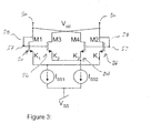
- the embodiment shown in Figure 3 is a transimpedence created from a cross-coupled pair transconductor.
- the input terminals 27 of the transconductor are connected by lines 28 to the output terminals 30.
- the cross coupled arrangements of FETS 20, 22, 24, 26 would take a differential voltage at input terminals 27 and provide a differential output current at terminals 30.
- a current received at terminals 30 causes a differential voltage between those terminals.
- the circuit has thus become a transimpedence with the input and output terminals being the same.
- the circuit of Figure 4 also includes a current source 44 and a cascode 46.
- the current source 44 allows the absolute current level at Junctions 45 to be adjusted as required.
- the cascode 46 decouples the voltage output at terminals 52 from the output of the current source.
- the common mode control circuit controls the absolute current level and hence absolute voltage levels at Vod output 52. This could operate, for example, by using a pair of resistors across terminals 52 (not shown) to sense the voltage level and provide feedback to the common mode control circuit.
- the voltage applied to the gates of FETS 71, 72 sets the current from the source 44.
- the DACs are digitally controlled current sources and so monotonic variations in current and hence gain of the amplifier is possible.
- the DACs themselves are known devices and need not be described further.
- FIG. 4B An alternative circuit is shown schematically in Figure 4B and comprises a transconductor 80 with input terminals 85 connected direct to a transimpedence 82 with output terminals 83.
- a transconductor 80 with input terminals 85 connected direct to a transimpedence 82 with output terminals 83.
- Such an arrangement could use the transimpedence as described in Figure 3 or other circuit and transconductance as in Figure 1 or 2, or other transconductance. Whilst such an arrangement would not have all the benefits of the circuit described, but it would function within the scope of an aspect of the invention.
Landscapes
- Engineering & Computer Science (AREA)
- Power Engineering (AREA)
- Physics & Mathematics (AREA)
- Nonlinear Science (AREA)
- Amplifiers (AREA)
Abstract
Description
- The present invention relates to an amplifier arrangement, in particular to a variable gain amplifier. The invention also relates to a transimpedence arrangement for use in an amplifier.
- Voltage amplification is needed in many semiconductor devices and various amplification arrangements are known. One example of the need for amplification is in DVD players in which a photodiode generates an output voltage from optical sensing of a DVD surface. Prior to digitising the voltage signal, gain is applied using an amplifier so that the voltage range is suited to the A to D converter. The voltage range received from the photodiode will vary depending upon the type of disk used: pre-recorded DVD disks produce higher voltage ranges due to high reflectivity and so need lower gain in contrast to recordable disks.
- We have appreciated the need for a variable gain amplifier for the above purpose and for other circuits also requiring variable voltage gain or attenuation. We have also appreciated the need for an improved amplifier arrangement having a wide, fully differential input and output voltage range, maximising the signal to noise ratio of the system, suitable for sub 2.5V power supply voltages. The invention is defined in the claims to which reference is now directed.
- A first aspect of the invention uses a matching transconductor and transimpedence circuit to provide voltage gain. An embodiment of this aspect uses a transconductor in the form of a cross-coupled differential pair of field effect transistors to provide an output current from a voltage input, and a transimpedence in the form of a cross-coupled differential pair of field effect transistors, with negative feedback from output to input, to provide a voltage output. The whole arrangement thereby provides gain, of course, gain can be negative (attenuation).
- The use of cross-coupled differential pairs provides a wide linear response. The use of matching transconductance and transimpedence arrangements ensures the gain is independent of process parameters, in the sense that the physical characteristics of production do not affect the performance because the active components are of the same type. Production variations are thus minimised.
- The embodying arrangement also includes control of the voltage gain and/or attenuation by varying the ratio current between the transconductance and transimpedence. The control current is programmed using current digital to analog converters (DACs). The ratio of the DAC current, and hence the programming of the gain and/or attenuation, can also be made independent of process parameters.
- A second aspect of the invention is a novel transimpedence arrangement comprising a transconductor with input connected to output with negative feedback. The embodiment is a cross-coupled differential pair with input connected to output, as used in the amplifier arrangement described above. The input and load linearisation leads to a small number of components in the signal path. The result is a wide bandwidth variable gain amplifier with a small group delay, which is both power and area efficient.
- A third aspect of the invention resides in an electronics device comprising the semiconductor integrated circuit discussed. Such device may be any consumer electronics device, for example, DVD players, set-top boxes, amplifiers, or any device in which voltage amplification is required. Particular embodiments are a DVD player (which includes a player capable of recording), and hard disk drives.
- An embodiment of the invention will now be described by way of example only and with reference to the figures in which:
- Figure 1:
- shows a known transconductor comprising a source coupled differential pair;
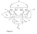
- Figure 2:
- shows a known transconductor comprising a cross-coupled differential pair;
- Figure 3:
- shows a transimpedence arrangement according to one aspect of the invention;
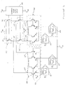
- Figure 4:
- shows an amplifier arrangement according to another aspect of the invention;
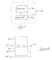
- Figure 4B:
- shows a functional view of an alternative arrangement to that of Figure 4; and
- Figure 5:
- shows an optical media device incorporating the invention.
- A known transconductor is shown in Figure 1. Briefly, the purpose of a transconductor is to convert a differential voltage input to a differential current output. Such devices are used in semiconductor circuits in which current mode signal processing is provided. The counterpart is a transimpedence which converts differential current to differential voltage. The transconductor shown comprises a
FET pair - The output current lo can be derived (as is known to the skilled person) to be:

- K is a constant related to the physical nature of the devices by K = Kn (W/L) where W = Width and L = Length of the active device (e.g. the FET channel).
- The input stage is thus linear only over a limited range of differential input voltage. The non-linearity can be seen by expanding
Equation 1 using a known McClaurin series to be:
- As can be seen, there is a linear gain term with Vid proportional to lo with the constant square root (2 IssK) and a non-linear term. To improve performance and reduce non-linearity a second known transconductor uses a cross-coupled differential pair, as shown in Figure 2. By selecting appropriate ratios of W/L for the devices (and hence the constant K=W/L), the non-linear term can be substantially cancelled. As shown in
Equation 2, the non-linear term is proportional to K. - And so choosing W/L to cancel these terms gives:

- The resulting linear transconductance of the circuit in Figure 2 is given by:

and therefore
- The width W and length L of devices are design choices and so selection of appropriate ratios allows the designer to cancel the third order (non-linear) term. The transconductance gm is the ratio of the applied voltage differential to the output differential current.
- We have appreciated that a linear transimpedence can be created from a transconductance by connecting the input of the transconductor to its output with negative feedback. An embodiment of this aspect of the invention is shown in Figure 3 applying the technique to the transconductance of Figure 2. The benefits of linearity of the transconductance are gained. Also, such a transimpedence has improved performance in comparison to resistive loads (which have tolerance issues) and op-amps (which have more components).
- The embodiment shown in Figure 3 is a transimpedence created from a cross-coupled pair transconductor. The
input terminals 27 of the transconductor are connected bylines 28 to theoutput terminals 30. When functioning as a transconductor, the cross coupled arrangements ofFETS input terminals 27 and provide a differential output current atterminals 30. However, with the input and output terminals connected, a current received atterminals 30 causes a differential voltage between those terminals. The circuit has thus become a transimpedence with the input and output terminals being the same. - The circuit functions as follows. Current injected into the drain of each
FET - The transimpedence circuit described is better than, say, a resistor which performs a similar current to voltage conversion, because resistors have poor tolerances, whereas the transimpedence described would depend on the ratios of W/L chosen to give a desired gm (transconductance) = IDIFF/VDIFF.
- Another aspect of the invention is an amplifier comprising a matching transconductor and transimpedence an embodiment of which is shown in Figure 4. In particular, the transimpedence is arranged as the one shown and described in relation to Figure 3. The variable gain amplifier comprises a transconductor 40 (as shown in Figure 2) having input terminals 50 and a transimpedence 42 (as shown in Figure 3) having output terminals 52. A voltage Vid at input terminals 50 is given variable gain and presented as output voltage Vod at output terminals 52 via an intermediate current at junctions 45. The amplifier thus converts voltage to current and then current to voltage and provides gain by adjusting the operation of the transconductance and transimpedence.
- The circuit of Figure 4 also includes a
current source 44 and acascode 46. Thecurrent source 44 allows the absolute current level at Junctions 45 to be adjusted as required. Thecascode 46, decouples the voltage output at terminals 52 from the output of the current source. - A common mode central circuit 48 provides voltage control to the current source and cascode to control their operation. The gain of the amplifier is varied using digital to analogue current sources/drains, shown as
current DACs 61, 62, 63, 64, which control the current through the transconductor and transimpedence. By controlling the current through thetransconductor 40, the differential current at intermediate Junction 45 is varied so that the voltage to current conversion has a variable transconductance. Similarly, the variable current through thetransimpedence 42 allows the transimpedence to be varied. - The overall gain of the amplifier is thus given by:

- The gain can be rewritten using equation 5 as:

- As explained above, the current produced by current DACs, D1, D2, D3, D4, shown as Iss1, Iss2, Iss3 and Iss4 are variable and are digitally programmable. Thus the gain of the whole circuit is programmable by the current DACs.
- As can be seen from Equation 7, the physical dimensions of the active devices (the FET channel) defined as width W and Length L govern the gain of the device. Choosing W/L1 = W/L3 and W/L2 = W/L4 optimises the variable gain amplifier operation around OdB. Choice of different W/L ratios, Iss1/Iss2 and Iss3/Iss4 ratios allows linearity to be optimised for different input and output voltage levels as well as for gain and/or attenuation.
- The operation of the circuit in Figure 4 will be explained now in terms of the current flowing. There are two different controls of the current flow:
- (i) The common mode control circuit 48 governs the current source by applying a controllable voltage to the gate of FETS 71 and 72. This sets the absolute current level at Junctions 45 and hence the current through
transimpedence 42; - (ii) The
DACs 61, 62, 63, 64 control the current flow into and out of the transconductor and transimpedence. This sets the variable gain level of the whole assembly. - The common mode control circuit controls the absolute current level and hence absolute voltage levels at Vod output 52. This could operate, for example, by using a pair of resistors across terminals 52 (not shown) to sense the voltage level and provide feedback to the common mode control circuit. The voltage applied to the gates of
FETS source 44. - The DACs are digitally controlled current sources and so monotonic variations in current and hence gain of the amplifier is possible. The DACs themselves are known devices and need not be described further. Consider, though, the currents at Junctions 45. The sum at this point must be such that the current from the transconductor equals the current to the transimpedence plus/minus the current from the current source.
- The
cascode 46 comprises a FET pair arranged in known manner so that Vds (drain/source) can change significantly for Vgs (gate/source) to change only slightly. The output impedance is the output impedance of the current source and the gain of the cascode. Varying the output voltage has little effect on the input and so the output and input are effectively decoupled. - The circuit described has a number of advantages over known amplifiers. First, a wide bandwidth is provided because bandwidth is a function of transductance and capacitance, and these are kept to a minimum because there are few components. The fewer RC paths in the circuit have better exponential settling. A wide voltage suitability is provided because of the variable absolute voltage settling.
- An alternative circuit is shown schematically in Figure 4B and comprises a transconductor 80 with input terminals 85 connected direct to a
transimpedence 82 withoutput terminals 83. Such an arrangement could use the transimpedence as described in Figure 3 or other circuit and transconductance as in Figure 1 or 2, or other transconductance. Whilst such an arrangement would not have all the benefits of the circuit described, but it would function within the scope of an aspect of the invention. - The amplifier circuit may be embodied in a variety of electronics devices, particularly optical media devices such as DVD or other disc players/ recorders. The amplifier is particularly suited to amplification of low level signals received from light detectors in such devices. A basic arrangement of an optical detector/ sensor 90 and an
amplifier 92 embodying the invention in amedia player 100 is shown in Figure 5.
Claims (10)
- An integrated circuit arranged to provide voltage gain, comprising:- a transconductor circuit (40) comprising a first cross-coupled differential pair having input terminals (50) arranged to receive a differential voltage and intermediate output terminals (45) arranged to produce a differential current; and- a transimpedence circuit (42) comprising a second cross-coupled differential pair with input and output connected with negative feedback and having input terminals (45) connected to the intermediate output terminals (45) and output terminals (52) arranged to produce a differential voltage output.
- An integrated circuit according to claim 1, wherein the transimpedence circuit comprises substantially the same circuit elements as the transconductor circuit.
- An integrated circuit according to claim 1 or 2, further comprising one or more variable current sources (61, 62, 63, 64) connected to the transconductor and/or the transimpedence arranged to vary the gain of the amplifier.
- An integrated circuit according to claim 3, wherein the one or more variable current sources are arranged so that the differential current at the intermediate output terminals is variable according to the variable current sources.
- An integrated circuit according to claim 3 or 4, wherein variable current sources comprise current DACs.
- An integrated circuit arranged as a transimpedence for converting a current to a voltage comprising a transconductor semiconductor circuit comprising a cross-coupled differential pair having an input and an output, wherein the transconductor input and output are connected so as to provide negative feedback.
- An electronics device comprising an integrated circuit according to any preceding claim.
- An optical media reader or writer comprising an integrated circuit according to any of claims 1 to 6.
- An optical disc player or recorder comprising a detector arranged to generate an output voltage from information on a disk and an integrated circuit according to any of claims 1 to 6 arranged to provide voltage gain of the output voltage.
- An electronics device comprising a detector for converting received light from an optical storage medium into electrical signals, and an amplifier arranged to amplify the electrical signals, comprising:- a transconductor circuit (40) comprising a first cross-coupled differential pair having input terminals (50) arranged to receive a differential voltage and intermediate output terminals (45) arranged to produce a differential current; and- a transimpedence circuit (42) comprising a second cross-coupled differential pair with input and output connected with negative feedback and having input terminals (45) connected to the intermediate output terminals (45) and output terminals (52) arranged to produce a differential voltage output.
Priority Applications (1)
| Application Number | Priority Date | Filing Date | Title |
|---|---|---|---|
| EP06252549A EP1858160A1 (en) | 2006-05-16 | 2006-05-16 | Amplifier arrangement |
Applications Claiming Priority (1)
| Application Number | Priority Date | Filing Date | Title |
|---|---|---|---|
| EP06252549A EP1858160A1 (en) | 2006-05-16 | 2006-05-16 | Amplifier arrangement |
Publications (1)
| Publication Number | Publication Date |
|---|---|
| EP1858160A1 true EP1858160A1 (en) | 2007-11-21 |
Family
ID=37076107
Family Applications (1)
| Application Number | Title | Priority Date | Filing Date |
|---|---|---|---|
| EP06252549A Withdrawn EP1858160A1 (en) | 2006-05-16 | 2006-05-16 | Amplifier arrangement |
Country Status (1)
| Country | Link |
|---|---|
| EP (1) | EP1858160A1 (en) |
Cited By (4)
| Publication number | Priority date | Publication date | Assignee | Title |
|---|---|---|---|---|
| WO2010035240A3 (en) * | 2008-09-26 | 2010-12-02 | Nxp B.V. | System and method for detecting movement of an object and integrated circuit implementation thereof |
| WO2013164088A3 (en) * | 2012-05-03 | 2014-02-13 | Universität Stuttgart | Circuit arrangement with tunable transconductance |
| EP3419164A4 (en) * | 2016-03-23 | 2019-03-13 | Mitsubishi Electric Corporation | VARIABLE GAIN AMPLIFIER |
| CN110504933A (en) * | 2019-08-07 | 2019-11-26 | 宁波大学 | A Highly Linear Variable Gain Amplifier |
-
2006
- 2006-05-16 EP EP06252549A patent/EP1858160A1/en not_active Withdrawn
Non-Patent Citations (4)
| Title |
|---|
| BEHZAD RAZAVI: "Prospects of CMOS Technology for High-Speed Optical Communication Circuits", IEEE JOURNAL OF SOLID-STATE CIRCUITS, IEEE SERVICE CENTER, PISCATAWAY, NJ, US, vol. 37, no. 9, September 2002 (2002-09-01), XP011065838, ISSN: 0018-9200 * |
| SCHAUMANN R ET AL: "Mixed-mode automatic tuning scheme for high-Q continuous-time filters", IEE PROCEEDINGS: CIRCUITS DEVICES AND SYSTEMS, INSTITUTION OF ELECTRICAL ENGINEERS, STENVENAGE, GB, vol. 147, no. 1, 4 February 2000 (2000-02-04), pages 57 - 64, XP006013833, ISSN: 1350-2409 * |
| STANISLAW SZCZEPANSKI ET AL: "A Linear Fully Balanced CMOS OTA for VHF Filtering Applications", IEEE TRANSACTIONS ON CIRCUITS AND SYSTEMS II: ANALOG AND DIGITAL SIGNAL PROCESSING, IEEE INC. NEW YORK, US, vol. 44, no. 3, March 1997 (1997-03-01), XP011012632, ISSN: 1057-7130 * |
| WYSZYNSKI A ET AL: "VHF highly linear fully-balanced CMOS OTA", PROCEEDINGS OF THE INTERNATIONAL SYMPOSIUM ON CIRCUITS AND SYSTEMS. (ISCS). CHICAGO, MAY 3 - 6, 1993, NEW YORK, IEEE, US, vol. VOL. 2, 3 May 1993 (1993-05-03), pages 1156 - 1159, XP010115309, ISBN: 0-7803-1281-3 * |
Cited By (5)
| Publication number | Priority date | Publication date | Assignee | Title |
|---|---|---|---|---|
| WO2010035240A3 (en) * | 2008-09-26 | 2010-12-02 | Nxp B.V. | System and method for detecting movement of an object and integrated circuit implementation thereof |
| US8698067B2 (en) | 2008-09-26 | 2014-04-15 | Nxp B.V. | System and method for detecting movement of an object and integrated circuit implementation thereof |
| WO2013164088A3 (en) * | 2012-05-03 | 2014-02-13 | Universität Stuttgart | Circuit arrangement with tunable transconductance |
| EP3419164A4 (en) * | 2016-03-23 | 2019-03-13 | Mitsubishi Electric Corporation | VARIABLE GAIN AMPLIFIER |
| CN110504933A (en) * | 2019-08-07 | 2019-11-26 | 宁波大学 | A Highly Linear Variable Gain Amplifier |
Similar Documents
| Publication | Publication Date | Title |
|---|---|---|
| US6356153B1 (en) | Rail-to-rail input/output operational amplifier and method | |
| EP1417752B1 (en) | High-bandwidth low-voltage gain cell and voltage follower having an enhanced transconductance | |
| WO1997045954A1 (en) | Variable gain cmos amplifier | |
| US7639076B2 (en) | Gain controlled amplifier and cascoded gain controlled amplifier based on the same | |
| US7911274B2 (en) | Variable transconductance circuit | |
| US7592869B2 (en) | Variable gain amplifier having dual gain control | |
| US6118340A (en) | Low noise differential input, differential output amplifier and method | |
| US6897701B2 (en) | Method and structure for improving the linearity of MOS switches | |
| US6208208B1 (en) | Operationally amplifying method and operational amplifier | |
| KR19990023418A (en) | Amplifier circuit and liquid crystal display device using same | |
| US20120098574A1 (en) | Filter circuit and optical disk device including the same | |
| EP1715579B1 (en) | Analogue multiplier | |
| US9287834B2 (en) | Read-out for MEMS capacitive transducers | |
| KR20090035358A (en) | Switched-Capacitor Variable Gain Amplifier with High Voltage Gain Linearity | |
| CN110380699A (en) | Input buffer, differential input buffer and integrated circuit | |
| JP5454366B2 (en) | Power amplifier module and portable information terminal | |
| US5859564A (en) | Differential amplifier circuit for use in a read channel for a magnetic recording system | |
| US7271651B2 (en) | High performance differential amplifiers with thick oxide devices for high impedance nodes | |
| KR100891221B1 (en) | Variable gain amplifier and filter circuit | |
| US10224951B2 (en) | Configurable input range for continuous-time sigma delta modulators | |
| JP2007174029A (en) | Gain variable circuit and automatic gain control amplifier using the same | |
| CN101485083A (en) | Variable gain amplifier having linear-in-dB gain characteristic | |
| KR20090032921A (en) | High Linearity Transconductance Amplifier | |
| US8212616B2 (en) | Biasing circuit for differential amplifier | |
| EP2779445A1 (en) | Three Stage Amplifier |
Legal Events
| Date | Code | Title | Description |
|---|---|---|---|
| PUAI | Public reference made under article 153(3) epc to a published international application that has entered the european phase |
Free format text: ORIGINAL CODE: 0009012 |
|
| AK | Designated contracting states |
Kind code of ref document: A1 Designated state(s): AT BE BG CH CY CZ DE DK EE ES FI FR GB GR HU IE IS IT LI LT LU LV MC NL PL PT RO SE SI SK TR |
|
| AX | Request for extension of the european patent |
Extension state: AL BA HR MK YU |
|
| 17P | Request for examination filed |
Effective date: 20080521 |
|
| 17Q | First examination report despatched |
Effective date: 20080623 |
|
| AKX | Designation fees paid |
Designated state(s): AT BE BG CH CY CZ DE DK EE ES FI FR GB GR HU IE IS IT LI LT LU LV MC NL PL PT RO SE SI SK TR |
|
| STAA | Information on the status of an ep patent application or granted ep patent |
Free format text: STATUS: THE APPLICATION IS DEEMED TO BE WITHDRAWN |
|
| 18D | Application deemed to be withdrawn |
Effective date: 20090702 |