EP1858132A2 - Method and apparatus for hot swap of line replaceable modules for ac and dc electric power systems - Google Patents
Method and apparatus for hot swap of line replaceable modules for ac and dc electric power systems Download PDFInfo
- Publication number
- EP1858132A2 EP1858132A2 EP07108115A EP07108115A EP1858132A2 EP 1858132 A2 EP1858132 A2 EP 1858132A2 EP 07108115 A EP07108115 A EP 07108115A EP 07108115 A EP07108115 A EP 07108115A EP 1858132 A2 EP1858132 A2 EP 1858132A2
- Authority
- EP
- European Patent Office
- Prior art keywords
- line
- hot swap
- module
- electrical
- pin
- Prior art date
- Legal status (The legal status is an assumption and is not a legal conclusion. Google has not performed a legal analysis and makes no representation as to the accuracy of the status listed.)
- Withdrawn
Links
Images






Classifications
-
- H—ELECTRICITY
- H02—GENERATION; CONVERSION OR DISTRIBUTION OF ELECTRIC POWER
- H02J—ELECTRIC POWER NETWORKS; CIRCUIT ARRANGEMENTS OR SYSTEMS FOR SUPPLYING OR DISTRIBUTING ELECTRIC POWER; SYSTEMS FOR STORING ELECTRIC ENERGY
- H02J1/00—Circuit arrangements for DC mains or DC distribution networks
- H02J1/10—Parallel operation of DC sources
-
- H—ELECTRICITY
- H02—GENERATION; CONVERSION OR DISTRIBUTION OF ELECTRIC POWER
- H02J—ELECTRIC POWER NETWORKS; CIRCUIT ARRANGEMENTS OR SYSTEMS FOR SUPPLYING OR DISTRIBUTING ELECTRIC POWER; SYSTEMS FOR STORING ELECTRIC ENERGY
- H02J1/00—Circuit arrangements for DC mains or DC distribution networks
- H02J1/001—Hot plugging or unplugging of load or power modules to or from power distribution networks
-
- H—ELECTRICITY
- H02—GENERATION; CONVERSION OR DISTRIBUTION OF ELECTRIC POWER
- H02J—ELECTRIC POWER NETWORKS; CIRCUIT ARRANGEMENTS OR SYSTEMS FOR SUPPLYING OR DISTRIBUTING ELECTRIC POWER; SYSTEMS FOR STORING ELECTRIC ENERGY
- H02J4/00—Circuit arrangements for mains or distribution networks not specified as AC or DC; Circuit arrangements for mains or distribution networks combining AC and DC sections or sub-networks
-
- H—ELECTRICITY
- H02—GENERATION; CONVERSION OR DISTRIBUTION OF ELECTRIC POWER
- H02J—ELECTRIC POWER NETWORKS; CIRCUIT ARRANGEMENTS OR SYSTEMS FOR SUPPLYING OR DISTRIBUTING ELECTRIC POWER; SYSTEMS FOR STORING ELECTRIC ENERGY
- H02J2105/00—Networks for supplying or distributing electric power characterised by their spatial reach or by the load
- H02J2105/30—Networks for supplying or distributing electric power characterised by their spatial reach or by the load the load networks being external to vehicles, i.e. exchanging power with vehicles
- H02J2105/32—Networks for supplying or distributing electric power characterised by their spatial reach or by the load the load networks being external to vehicles, i.e. exchanging power with vehicles for aircrafts
-
- Y—GENERAL TAGGING OF NEW TECHNOLOGICAL DEVELOPMENTS; GENERAL TAGGING OF CROSS-SECTIONAL TECHNOLOGIES SPANNING OVER SEVERAL SECTIONS OF THE IPC; TECHNICAL SUBJECTS COVERED BY FORMER USPC CROSS-REFERENCE ART COLLECTIONS [XRACs] AND DIGESTS
- Y02—TECHNOLOGIES OR APPLICATIONS FOR MITIGATION OR ADAPTATION AGAINST CLIMATE CHANGE
- Y02T—CLIMATE CHANGE MITIGATION TECHNOLOGIES RELATED TO TRANSPORTATION
- Y02T50/00—Aeronautics or air transport
- Y02T50/50—On board measures aiming to increase energy efficiency
Definitions
- the present invention relates to electric power systems, and more particularly to a method and apparatus for hot swap of modules for electric power systems.
- Electric systems used in complex environments such as aerospace systems, more electric aircraft systems, industrial environments, vehicles, etc., include a large number of electric modules.
- Various electric modules may need to be extracted and replaced with other electric modules, to change functionality or to replace electric modules that exhibit faults.
- Hot swap, hot-plug, and hot-dock are terms used interchangeably to refer to the process of safely inserting or removing cards, PC boards, cables, and/or modules from a host system without removing power.
- the goal of hot swap is to insert or remove modules without disturbing, damaging, or degrading up/down-stream adjacent line replaceable modules/ subsystems, to increase system availability, reduce down time, simplify system repair, and allow for system maintenance/upgrade without interrupting service to other loads.
- hot swap can cause severe electrical, mechanical, thermal and operational problems in an electrical system.
- random pin arcing may occur during the mating process of a replaceable module with its parent electrical system.
- Pulling a board/module out while there is current passing through the module connectors, or inserting a board/module with all bulk/bypass capacitors at zero volts, can introduce severe electrical voltage/ current transients which may adversely impact reliability and to safety consequences.
- current chopping introduces Ldi / dt variations (where L is inductance of a load, for example) leading to very large voltage transients which are a major safety concern for maintenance people, as large voltage transients can cause high voltage electrical shock.
- LRMs line replaceable modules
- PS-LRM Power Supplies
- DC-LRM Digital Controllers
- AC-SSPC-LRM AC Solid-State-Remote-Controllers
- DC-SSPC-LRM DC Solid-State-Remote- Power-Controllers
- SSSDs AC Solid State Switching Devices
- Such AC and DC power systems may have AC voltages of 115 or 230V, or higher, with fixed frequencies (for example, 50/60 Hz or 400Hz), or variable frequencies (for example 360-800Hz for aerospace applications), or DC voltages levels such as, for example, 28V or 270V.
- the power of such AC or DC systems may depend on the number of channels and current rating and voltage of each channel.
- an AC LRM for the Airbus A380 aircraft has 8 channels.
- Such AC and DC LRM boards are currently being deployed in aerospace and industry, and are poised to eventually replace traditional electromechanical AC/DC circuit breakers or relays, to reduce the overall system cost and weight, and improve reliability.
- a hot swap system for hot swap of modules includes a connector with long and short pins, a fuse, and an RC circuit.
- the long pins mate first, adding the RC circuit to precharge the module/board.
- the short pins mate, bypassing the resistor connected to the longer pins and creating a low impedance connection.
- This technique does not detect board/module insertion or extraction at the beginning of the hot swap process in order to prevent disturbances to various data lines.
- This technique also does not communicate with the remaining software of the larger electrical system to prevent further abnormal operation or possible damage on circuits surrounding the modules/boards that are hot-swapped.
- a disclosed embodiment of the application addresses these and other issues by utilizing a method and apparatus for hot swap of modules for AC and DC electric power systems that use either low or high supply voltages.
- the method and apparatus prevent random pin arcing during mating process by reducing the AC or DC current during the MAKE or BREAK process; eliminate in-rush currents during initial insertion of a board/module with all bulk/bypass capacitors at zero volts; prevent current chopping when a board is pulled-out when there is a load current in a normal or fault situation; eliminate large electrical voltage/ current transients, such as large voltage transients due to Ldi / dt current chopping variations, which may adversely impact reliability and lead to safety consequences; detects the process of a board/LRM insertion or extraction.
- the method and apparatus for hot swap of modules for AC and DC electric power systems can be used for both low and high power systems.
- an apparatus for hot swap of AC or DC line replaceable modules comprises: a pin assembly, the pin assembly being connectable to a module and connectable to a backplane, the pin assembly resistively reducing a current associated with the module during disconnection of the module from the backplane, and presenting a high resistance to the module during connection of the module to the backplane, and a low resistance to the module at completion of the connection of the module to the backplane; and a hot swap detector connectable to the pin assembly, the hot swap detector detecting the disconnection of the module from the backplane, and detecting the connection of the module to the backplane.
- an apparatus for hot swap of AC or DC line replaceable modules comprises: a first hot swap protection circuit connected to a first electrical line and a second electrical line, wherein the first electrical line and the second electrical line are connectable to a line replaceable module, the first hot swap protection circuit including two first line diodes connected to the first line, one of the two first line diodes being forward biased from the first line and the other of the two first line diodes being reverse biased from the first line, and two second line diodes connected to the second line, one of the two second line diodes being forward biased from the second line, the other of the two second line diodes being reverse biased from the second line, the second line diode forward biased from the second line being connected at a first point to the first line diode forward biased from the first line, and the second line diode reverse biased from the second line being connected at a second point to the first line diode reverse biased from the first line.
- an apparatus for hot swap of AC or DC line replaceable modules comprises: a hot swap protection circuit connected to a first electrical line and a second electrical line, wherein the first electrical line and the second electrical line are included in a line replaceable module, the first hot swap protection circuit including two first line diodes connected to the first line, one of the two first line diodes being forward biased from the first line and the other of the two first line diodes being reverse biased from the first line, two second line diodes connected to the second line, one of the two second line diodes being forward biased from the second line, the other of the two second line diodes being reverse biased from the second line, the second line diode forward biased from the second line being connected at a first point to the first line diode forward biased from the first line, and the second line diode reverse biased from the second line being connected at a second point to the first line diode reverse biased from the first line, and a capacitor and a resistor, wherein the resistor is connected in series with
- a method for hot swap of AC or DC line replaceable modules comprises: capturing front end stored energy in front end inductances of a front end of an electrical system during exaction of a line replaceable module, the step of capturing front end stored energy using a first electrical line and a second electrical line of the front end, two first line front end devices connected to the first line, one of the two first line front end devices being forward biased from the first line and the other of the two first line front end devices being reverse biased from the first line, and two second line front end devices connected to the second line, one of the two second line front end devices being forward biased from the second line, the other of the two second line front end devices being reverse biased from the second line, the second line front end device forward biased from the second line being connected at a first point to the first line front end device forward biased from the first line, and the second line front end device reverse biased from the second line being connected at a second point to the first line front end device reverse biased from the first line.
- FIG. 1 is a general functional block diagram of a subassembly electrical system containing line replaceable modules (LRMs) with hot-swap capability according to an embodiment of the present invention
- FIG. 2 is a block diagram of an electrical configuration containing a system for hot swap of line replaceable modules according to an embodiment of the present invention
- FIG. 3A is a block diagram illustrating an exemplary implementation of a hot swap protection system using short/long pins according to an embodiment of the present invention illustrated in FIG. 2;
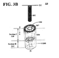
- FIG. 3B illustrates a pin arrangement for hot swap that reduces the number of pins and integrates a hot swap resistor into the pin arrangement according to an embodiment of the present invention illustrated in FIG. 2;
- FIG. 4 is a block diagram of an electrical configuration containing a system for hot swap of line replaceable modules according to a second embodiment of the present invention
- FIG. 5A illustrates a DC SSPC LRM without hot swap protection circuits
- FIG. 5B is a block diagram illustrating an exemplary implementation of hot swap protection for a DC SSPC LRM according to a second embodiment of the present invention illustrated in FIG. 4;
- FIG. 5C illustrates in more detail a hot swap protection block for use with a DC SSPC LRM according to a second embodiment of the present invention illustrated in FIG. 5B;
- FIG. 5D illustrates in more detail another implementation for a hot swap protection block for use with a DC SSPC LRM according to a second embodiment of the present invention illustrated in FIG. 5B;
- FIG. 6A illustrates an AC SSPC LRM without hot swap protection circuits
- FIG. 6B is a block diagram illustrating an exemplary implementation of hot swap protection for an AC SSPC LRM according to a second embodiment of the present invention illustrated in FIG. 4;
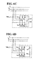
- FIG. 6C illustrates in more detail a hot swap protection block for use with an AC SSPC LRM in a three phase system according to a second embodiment of the present invention illustrated in FIG. 6B;
- FIG. 6D illustrates in more detail another implementation for a hot swap protection block for use with an AC SSPC LRM in a three phase system according to a second embodiment of the present invention illustrated in FIG. 6B;
- FIG. 6E illustrates in detail a hot swap protection block for use with an AC SSPC LRM in a single phase AC system according to a second embodiment of the present invention illustrated in FIG. 4;
- FIG. 6F illustrates in detail a single phase hot swap protection block for use with an AC SSPC LRM in a three phase AC system according to a second embodiment of the present invention illustrated in FIG. 4;
- FIG. 6G illustrates in detail another implementation for a hot swap protection block for use with an AC SSPC LRM in a single phase AC system according to a second embodiment of the present invention illustrated in FIG. 4.
- FIG. 1 is a general functional block diagram of a subassembly electrical system containing line replaceable modules (LRMs) with hot-swap capability according to an embodiment of the present invention.
- the electrical system 100 illustrated in FIG.1 includes the following components: power systems 20; m line replaceable modules (LRMs) 40_1 , ..., 40_m of which LRM 40_m is shown; circuitry, control and load systems 50; m backplane connectors 104_1, 104_2 , ..., 104_m ; and a backplane protection system 191. Operation of the electrical system 100 in FIG.1 will become apparent from the following discussion.
- LRM 40_m includes a protection module 30_m ; a hot swap detector 134_m ; other circuitry 171_m ; a controls and arbitration logic unit 144_m ; and pin systems 183_m and 173_m .
- Backplane connector 104_m includes pin systems that connect /disconnect from LRM 40_m pin systems, when LRM 40_m is inserted/extracted from backplane connector 104_m .
- Backplane connectors 104_1, 104_2, 104_3, etc. also connect or disconnect from LRMs 40_1, 40_2, 40_3 , etc. (not shown).
- circuitry 171_m includes electronic and electric components of line replaceable module 40_m , such as transistors, resistors, connectors, switches, etc.
- Hot swap detector 134_m , protection module 30_m , and pin system 183_m perform hot swap protection functions during insertion or extraction of LRM 40_m .
- Controls and arbitration logic unit 144_m communicates with hot swap detector 134_m and with other circuitry 171_m.
- Replaceable modules 40_1, 40_2, ..., 40_m can be connected to and separated from backplane connectors 104_1, 104_2, ..., 104_m , which provide electrical power to replaceable modules.
- Some LRMs may connect to two backplane/motherboard connectors, one connector for power-pins and one for low voltage power supply input and discrete I/O lines for controls, signal sensing, etc.
- Power-in or power-out lines and other discrete signals may first be routed to the motherboard/backplane connectors. Then, when one LRM is attached to the corresponding mating backplane connector, proper power, control and power supply lines are connected from the backplane to the proper connector pins on the LRM, establishing the right connections (achieved by design) to get the desired functionality provided by that particular LRM.
- Backplane connectors 104_1, 104_2, ..., 104_m connect to backplane protection system 191.
- Backplane protection system 191 includes electric and electronic components such as switches, fuses, circuit breakers, resistors, etc., for protection of the backplane connectors.
- Input I/P power lines 123 lead into backplane protection system 191 and provide power from power systems 20.
- Control I/O lines 125 transport control I/O data in and out from backplane protection system 191, hence communicating control I/O data to replaceable modules 40_1, 40_2, ..., 40_m .
- Output O/P power lines 127 leave backplane protection system 191 and connect to circuitry, control and load systems 50.
- Protection module 30_m protects replaceable module 40_m and backplane connector 104_m from in-rush currents during insertion of replaceable module 40_m into the backplane connector 104_m and electrical system 100, and from transient voltages and current chopping during extraction of replaceable module 40_m from backplane connector 104_m and electrical system 100. Protection module 30_m performs protection functions together with pin system 183_m . Inside replaceable module 40_m , protection module 30_m protects other circuitry 171_m . Protection module 30_m also protects the power systems 20, the circuitry, control and load systems 50, during hot swap of replaceable module 40_m .
- Protection module 30_m protects components of electrical system 100 during hot swap insertion or removal of replaceable module 40_m under normal or faulty modes of operation for high voltage DC and AC systems without the need to disconnect power. Protection modules 30_m permits safe and reliable insertion and removal of different types of LRMs during hot swap, without disturbing, damaging, or degrading up/down-stream adjacent LRMs and subsystems of electrical system 100. Protection module 30_m also helps high voltage AC and DC load management LRMs to control the flow of electrical power to internal and external circuitry/loads and achieve proper protection of SSSDs or the wiring system.
- Electrical system 100 may be associated with an aircraft, a more electric aircraft, a ship, a laboratory facility, an industrial environment, etc.
- the power systems 20 provide electrical energy in electrical system 100.
- the power systems 20 may include multiple power supply inputs, for redundancy.
- the power systems 20 may include AC and DC power supplies, electrical components such as transformers, inductances, resistances, etc.
- the power systems 20 may provide high DC or AC voltages or low DC or AC voltages to replaceable modules 40_1, 40_2 , ..., 40_m .
- Power systems 20 may provide and replaceable modules may use various AC voltages, such as, for example, 115V or 230V or higher, with fixed frequencies (such as, for example, 50/60 Hz or 400Hz), or variable frequencies (such as, for example 360-800Hz for aerospace applications), or DC voltages such as, for example, 28V or 270V.
- the power of replaceable module 40_m may depend on the number of channels, as well as current rating and voltage of each channel.
- Replaceable modules 40_1, 40_2, ..., 40_m receive electric power from power systems 20.
- Replaceable modules 40_1 , .... 40_m may be AC or DC Line Replaceable Modules (LRMs), cards, PC boards, etc.
- Replaceable modules 40_1 , 40_2 , ..., 40_m may be high voltage AC and DC LRMs.
- Replaceable modules 40_1 , 40_2, ..., 40_m may have on-board Solid State Switching Devices (SSSDs).
- Replaceable modules 40_1 , 40_2 , ..., 40_m may be high voltage Solid State AC and DC switches, referred to in the industry as Solid State Remote Power Controllers (SSPCs).
- SSPCs Solid State Remote Power Controllers
- Replaceable modules 40_1 , 40_2 , ..., 40_m may be various types of LRMs such as: Power Supplies (PS-LRM), Digital Controllers (DC-LRM), AC Solid-State-Remote-Controller (AC-SSPC-LRM), DC Solid-State-Remote-Controller (DC-SSPC-LRM), LRMs used for aircraft platforms and More Electric platforms, PC boards or cards, etc.
- Solid State AC and DC switches can be used with a wide range of powers, from a few Watts to hundreds of KWatts.
- Replaceable modules 40_1 , 40_2 , ..., 40_m including AC and DC Solid State Switching Devices (SSSDs) may manage high voltage AC and DC powers and loads, and may control the flow of electrical power to internal and external circuitry/loads, to achieve proper protection based on i 2 ⁇ t (instantaneous overcorrect protection for large currents and proportionally time-delayed overload protection for smaller currents) to protect the SSSDs or the wiring system.
- SSSDs Solid State Switching Devices
- Circuitry, control and load systems 50 receive electrical power through the replaceable modules, and use the electrical power downstream.
- Circuitry, control and load systems 50 may include various electrical systems, such as systems on an aircraft or ship, navigation systems, cabin systems, air conditioning systems, etc., systems in an industrial facility such as electrical equipment and tools, etc.
- Circuitry, control and load systems 50 may include power pins, DC and AC loads, electric circuits using DC and AC power that enable functioning of various services onboard a vehicle, or in a complex environment such as a laboratory facility. Services using AC and DC power may be an electric motor, an automatic braking system, a lighting system of a vehicle, a piece of industrial equipment, etc.
- Each LRM among LRMs 40_1, 40_2 , ..., 40_m-1 includes a protection module like protection module 30_m of LRM 40_m .
- Protection modules ensure that hot swap of modules is properly done. Protection modules avoid random pin arcing during mating process of a replaceable module to electrical system 100. Protection modules provide protection for safely inserting a board/module when the board is not electrically initialized, and for safely pulling a board-out while there is current passing through connectors. When electrical system 100 includes integrated systems, protection modules provide hot swap protection beyond local boundaries of the replaceable modules.
- protection modules mitigate hot swap effects, so that various bus activities & other operations taking place in electrical system 100 are not disturbed when hot swap of one or more replaceable modules is occurring. Together with control systems of electrical system 100, protection modules help establish autonomy of subsystems in electrical system 100 and automatic system reconfiguration based on the type of replaceable modules extracted or inserted. Information needed to describe the LRM type can be hard-wired through adjustable jumper connectors and/or backed-up by S/W into non-volatile memory locations readable to processor units during LRM initialization.
- Replaceable modules 40_1, 40_2 , ..., 40_m and the associated protection modules are designed to provide electrostatic discharge (ESD) protection during hot swap, because electrostatic discharges can disable ports by destroying interface ICs, replaceable modules connections, and surrounding electrostatic sensitive subsystems.
- ESD electrostatic discharge
- FIG. 2 is a block diagram of an electrical configuration 154 containing a system for hot swap of line replaceable modules according to an embodiment of the present invention.
- the electrical configuration 154 illustrated in FIG. 2 includes the following components: a backplane 104; a replaceable module 40A; and a backplane protection system 191.
- the electrical configuration 154 is included in electrical system 100.
- Replaceable module 40A may be a line replaceable module (LRM), and includes: a protection module 30; a hot swap detector 134; other circuitry 171; a controls and arbitration logic unit 144; and pin systems 183 and 173.
- Backplane 104 includes pin systems 181 and 175.
- Other circuitry 171 includes electronic and electric components of line replaceable module 40A, such as transistors, resistors, connectors, switches, etc.
- Hot swap detector 134, protection module 30, and pin system 183 perform hot swap protection functions.
- Replaceable module 40A can be connected to and separated from backplane 104, which provides electrical power to replaceable module 40A.
- Replaceable module 40A connects and separates through pin systems 183 and 173 from backplane 104, at backplane pin systems 181 and 175.
- Backplane 104 provides electrical power to controls and arbitration logic unit 144 when pin systems 173 and 175 mate.
- Backplane 104 provides electrical power to protection module 30 and hot swap detector 134 when pin systems 183 and 181 mate.
- Pin system 183 includes a number of pins, of which pins a, b, c, d, and e are shown. Pins of pin system 183 connect to protection module 30 and hot swap detector 134.
- Pin system 173 includes power supply and controls pins, of which pins f, g , h , i , j , and k are shown. Pins of pin system 173 connect to controls and arbitration logic unit 144. Controls and arbitration logic unit 144 also communicates with hot swap detector 134.
- Backplane pin system 181 includes power pins of which pins l, m, n, o, and p are shown. Backplane pin system 181 connects to backplane protection system 191. Backplane protection system 191 includes electric and electronic components such as switches, fuses, circuit breakers, resistors, etc., for protection of backplane 104. Input I/P power lines 123 lead into backplane protection system 191. Control I/O lines 125 transport control I/O data in and out from backplane protection system 191, hence communicating control I/O data to replaceable module 40A. Output O/P power lines 127 leave backplane protection system 191 and connect to loads.
- Backplane pin system 175 includes power supply input pins q and r, and control pins and discrete I/O pins of which pins s, t, u , and v are shown. Power supply input pins q and r connect to backplane protection system 191 through power supply inputs 185. The control pins and discrete I/O pins of backplane pin system 175 also connect to backplane protection system 191.
- Protection module 30 protects replaceable module 40A and backplane 104 from in-rush currents during insertion of replaceable module 40A into the backplane 104 and electrical system 100, and from transient voltages and current chopping during extraction of replaceable module 40A from backplane 104 and electrical system 100. Protection module 30 performs protection functions together with pin system 183. Inside replaceable module 40A, protection module 30 protects other circuitry 171.
- Hot swap detector 134 includes electronic circuitry (further described in FIG. 3A) that senses changes in electrical parameters associated with protection module 30 and pin system 183. Based on these changes, hot swap detector 134 detects whether a hot swap (insertion or extraction) of replaceable module 40A is being performed or has been completed. Hot swap detector 134 also detects changes in electrical parameters associated with other circuitry 171, changes which may occur during hot swap.
- Controls and arbitration logic unit 144 receives reports from hot swap detector 134 about completion of hot swap of replaceable module 40A. When hot swap insertion of replaceable module 40A is completed, controls and arbitration logic unit 144 starts normal control and communication functions inside replaceable module 40A and at control pins and discrete I/O pins in pin system 175.
- FIG. 3A is a block diagram illustrating an exemplary implementation of a hot swap protection system using short/long pins according to an embodiment of the present invention illustrated in FIG. 2.
- FIG. 3A shows how short/long pin can be used to prevent random pin arcing during the mating process by reducing the DC current during the MAKE (insertion) or BREAK (extraction) process for a DC LRM. Similar methods and apparatus apply for hot swap of AC type LRMs.
- FIG. 3A illustrates a DC Solid-State Remote Controller Line Replaceable Module (DC SSPC LRM) 40A included in an electrical configuration 154A.
- the DC SSPC LRM includes: high voltage Solid State DC switches, which are Solid State Power Controllers (SSPCs); a hot swap detector 134; a control and arbitration logic unit 144; an active or passive diode ORing system 232; a power connector 225, and a second power strip 226; and a plurality of pins connected to the power connectors.
- SSPCs Solid State Power Controllers
- a few SSPCs are shown as SSPC #1 (element 41A) and SSPC#2 (element 41B) More SSPCs may be present but are not shown in the picture.
- the SSPCs are connected to electrical rail 244 through fuses. For example, SSPC#1 41A is connected to electrical rail 244 through fuse 241.
- the control logic voltage is applied first when a DC SSPC LRM is inserted during hot swap.
- the power pins are applied after the control logic voltage is applied.
- Hot swap detector 134 connects to power connector 225 and bulk capacitors, and to pins 220, 221, and 223. Bulk capacitors are typically present on the DC LRM.
- SSPC#1 41A also connects to pins 223 and 221. Initially, pin 223 charges the bulk capacitors on the board. Pin 223 then gets shorted-out by pin 221.
- Hot swap detector 134 detects the hot swap by detecting the voltage on the bulk capacitors, and informs the controls and arbitration logic unit 144, when the hot swap is completed (i.e., board fully inserted).
- Hot swap detector 134 communicates with the controls and arbitration logic unit 144 through line 235, and reports whether a hot swap is in progress or has been completed. After the hot swap is reported to be complete, controls and arbitration logic unit 144 communicates normally with SSPC#1 41A, through communication port 237 and discrete I/O signal and control port 238, through the isolation section 236. SSPC#1 41A also connects to the power connector 225 at male contact 218 L' 1 , which connects to the backplane 104 at female contact 217 L 1 . A second SSPC #2 41B may similarly connect to the controls and arbitration logic unit 144, and to the backplane 104 at contacts L' 2 and L 2 .
- An N th SSPC #N may similarly connect to the controls and arbitration logic unit 144, and to the backplane 104 at male contact 219 (L' N ) and female contact 215 (L N ).
- the pins 220, 221, 222 and 223 communicate with the backplane 104 at female contacts 214, 213, 212 and 211.
- Reverse actions take place when a board is being pulled-out.
- resistor R1 (element 243).
- Resistor R1 243 connects to SSPC#1, SSPC#2, etc., through line 244.
- Resistor R1 243 connects to hot swap detector 134 as well, and hot swap detector 134 detects when extraction of SSPC #1 has been completed.
- Resistor R1 243 also contributes to detection of LRM insertion by hot swap detector 134.
- Block 232 provides passive or active diode ORing of a redundant power supply input from multiple power sources for the control power supply of the LRM.
- Block 232 allows connection of multiple power supply voltage inputs to realize a fault tolerant power supply bus for the LRM.
- Block 232 includes an integrated active-diode-OR circuit which provides soft power-up/down capability, avoids excessive power losses and voltage drops, and controls voltage/current transients and in-rush OR current chopping during LRM insertion/extraction respectively.
- Passive or active diode ORing block 232 connects to a 5V bus 233, which also connects to SSPC#1, and to the other SSPCs present on the DC SSPC LRM. Passive or active diode ORing block 232 communicates with controls and arbitration logic unit 144 at a discrete I/O port.
- Unit 291 provides regulated DC-DC power conversion.
- unit 291 provides regulated DC-DC power conversion from 5V-to-5V, or from 5V-to-3.5V, etc.
- Unit 291 may also provide isolation if required.
- the motherboard/ backplane includes sections 227 and 224.
- the mating connectors 217, 216, 215, 214, 213, 212 and 211 in section 224 are part of the motherboard/ backplane and are fixed.
- the mating connectors in the backplane section 227 are also fixed.
- DC SSPC LRM) 40A can be inserted or extracted from the motherboard/ backplane.
- the short/long pin arrangement is used for detection and proper mitigation of hot swap during insertion or extraction of LRM/boards.
- This arrangement eliminates in-rush currents during the initial insertion of a board/module with all bulk/bypass capacitors at zero volts.
- the short/long pin arrangement illustrated in FIG. 3A also prevents current chopping when a board/LRM is pulled-out while there is a load current, in a normal or fault situation.
- the protection circuit shown in FIG. 3A prevents current chopping and also eliminates large transient voltages due to inductive current variations Ldi / dt. Pulling a board out without the hot swap protection while there is inductive current passing through connector pins may cause current chopping which results in arcing and excessive voltage/current transients.
- Inductive current may be due to on-board inductive filters or inductive loads, for example. Arcing and excessive voltage/current transients can have severe safety consequences due to risk of voltage shock to personnel or to other subsystems during failure modes or faulty conditions, such as short circuit conditions.
- FIG. 3B illustrates a pin arrangement 320 for hot swap that reduces the number of pins and integrates a hot swap resistor into the pin arrangement according to an embodiment of the present invention illustrated in FIG. 2.
- FIG. 3B an alternative method of hot swap pin arrangement is shown.
- Pin 304 has two sections, section I (310) and section II (312).
- Section I (310) comprises an inner resistive cylinder 306 placed in a protective insulating sheet 307.
- Section II (312) comprises a conductive shell 308.
- the resistance of the pin arrangement 320 between points M and N is initially high, and then starts decreasing as the solid male pin conductor 302 travels inside through section I (310) of the female pin 304.
- the resistance of pin arrangement 320 becomes zero, as the conductive shell 308 of section II (312) shorts out the resistance of section I (310).
- the resistive section I (310) performs the functions of hot swap resistor R1 243 from FIG. 3A.
- the resistance of the pin arrangement 320 gradually increases as male pin conductor 302 travels out of the female pin 304, and interruption current due to LRM extraction is reduced to a safe amount for the LRM and other subsystems of electrical system 100.
- the process of long/short pin can be extended to multiple pins and accompanying resistors to achieve a more uniform hot swap in a discrete fashion.
- a long/medium/short pin system can be used, with two accompanying resistors, R1 and R2, to obtain an additional level of protection during hot swap.
- FIG. 4 is a block diagram of an electrical configuration 410 containing a system for hot swap of line replaceable modules according to a second embodiment of the present invention.
- Electrical configuration 410 is included in electrical system 100.
- the electrical configuration 410 illustrated in FIG. 4 includes the following components: power source modules 20A; load modules 50A; replaceable modules 40C with LRM protection module 30B; backplane protection modules 30C and 30D; motherboard protection module 30D; and motherboard/ backplane 104.
- Power source modules 20A are included in power systems 20 of FIG. 1.
- Load modules 50A are included in circuitry, control and load systems 50 of FIG. 1.
- LRM protection module 30B protects replaceable modules 40C during hot swap. LRM protection module 30B may be included in replaceable modules 40C.
- Backplane protection module 30C protects power source modules 20A during hot swap of replaceable modules 40C.
- Backplane protection module 30D protects load modules 50A during hot swap of replaceable modules 40C.
- Backplane protection modules 30D and 30C also protect the motherboard/ backplane 104.
- FIG. 5A illustrates a DC SSPC LRM without hot swap protection circuits.
- the system 410A in FIG. 5A includes a DC SSPC LRM 40C, a front end DC source circuit, and a plurality of loads.
- the front end DC supply 521 generates the current i S , which passes through front end inductance L S 522 and through the joined connectors A and B (523).
- Joined connectors C and D (524) provide DC return for the DC current.
- Joined connectors E and F (525) provide a ground connection for DC SSPC LRM 40C, at chassis ground 526.
- the current is then passes through the DC SSPC LRM 40C where it splits into components i 1 , i 2 , ..., i n that pass through a plurality of SSPCs.
- SSPC#1 41C, SSPC#2 41D, ..., SSPC#N 41E are connected inside DC SSPC LRM 40C through fuses 534, 535, ...,536.
- the chassis 526 is a hard cover LRM chassis at ground potential that provides electrostatic discharge (ESD) protection during hot swap of DC SSPC LRM 40C.
- ESD electrostatic discharge
- the hard cover LRM chassis 526 at ground potential provides proper ESD protection during hot swap of DC SSPC LRM 40C.
- FIG. 5B is a block diagram illustrating an exemplary implementation of hot swap protection for a DC SSPC LRM 40C according to a second embodiment of the present invention illustrated in FIG. 4.
- Fig. 5B shows the DC SSPC LRM 40C from FIG. 5A, with hot swap protection circuits.
- Hot swap protection circuits in FIG. 5B are implemented for capturing stored energy in the front end inductance L S 522 and in load inductances Load#1 527, Load#2 528, ..., Load#N 529, when the DC SSPC LRM board 40C is extracted under load, or when one or more of the controlled SSSD devices included in DC SSPC LRM board 40C have failed short.
- Hot swap protective block 540 has been introduced in FIG. 5B at the front-end supply end between electrical lines AB and CD.
- Hot swap protective block 540 may include standard RC snubbers, surge protection devices, or the exemplary circuit shown in FIG. 5C, to mitigate the current chopping problem on the board side caused by the front end inductance 122.
- Hot swap protective block 540 protects the mother board and the front-end supply side.
- a free-wheeling diode 555 has also been introduced at the front end side of the circuit in FIG. 5B for protection of the front-end circuit side during hot swap.
- Free-wheeling diodes DL1 537, DL2 538,..., DLN 539 are introduced for the protection of the load-side connectors.
- Free-wheeling diode DL1 537 protects the SSPC#1 41C and the load inductance Load#1 527 from current/voltage transients generated during hot swap;
- free-wheeling diode DL2 538 protects the SSPC#2 41D and the load inductance Load#2 528; and so on, for all N SSPCs and loads.
- FIG. 5C illustrates in more detail the hot swap protection block 540 for use with DC SSPC LRM 40C according to a second embodiment of the present invention illustrated in FIG. 5B.
- Hot swap protection block 540A includes diodes 540_1, 540_2, 540_3, 540_4, a capacitor 540_5, and a resistor 540_6.
- Hot swap protection block 540A connects to lines AB and CD in the circuit shown in FIG. 5B.
- Protection block 540A steers currents generated during hot swap by inductance L S 522, through resistor 540_6 so that such currents do not circulate through the lines going to and coming from DC SSPC LRM 40C.
- Protection block 540A also applies transient voltages generated during hot swap at the front-end side, to capacitor 540_5 and resistor 540_6 so that such voltages do not cause transient currents on the front-end supply side or through the DC SSPC LRM 40C.
- FIG. 5D illustrates in more detail another implementation for hot swap protection block 540 for use with DC SSPC LRM 40C according to a second embodiment of the present invention illustrated in FIG. 5B.
- Hot swap protection block 540B includes diode block 540-8, capacitor 540_5, and resistor 540_6 in series with the capacitor 540_5.
- Diode block 540-8 includes diodes, which can be arranged in the configuration shown in FIG. 5C, that is, the configuration of diodes 540_1, 540_2, 540_3, 540_4.
- Hot swap protection block 540B connects to lines AB and CD in the circuit shown in FIG. 5B.
- the configuration shown in FIG. 5D is advantageous as it eliminates initial power in-rush for the capacitor 540_5 and reduces overall power dissipation as the capacitor 540_5 gets charged up and then current ceases to flow in the resistor 540_6.
- FIGS. 5B, 5C and 5D were discussed in the context of a DC SSPC LRM, the hot swap protection systems in FIGS. 5B, 5C and 5D are equally applicable to hot swap protection of other types of modules, circuits, and systems.
- FIG. 6A shows an AC SSPC LRM without hot swap protection circuits.
- the system 410B in FIG. 6A includes an AC SSPC LRM 40D, a front end AC source circuit, and a plurality of loads.
- the front end 3-phase alternating current AC power system 617, 618 and 619 generate AC currents that pass through front end inductances 622, 624 and 626 and through joined connector systems 631, 633, 635 and 637.
- Joined connector system 639 provides a ground connection for AC SSPC LRM 40D, at the chassis ground 640.
- the currents from the front-end AC source circuit pass through the AC SSPC LRM 40D to a plurality of SSPCs, namely AC SSPC1 41F, AC SSPC2 41G, and AC SSPC3 41H.
- AC SSPC1 41F, AC SSPC2 41G, and AC SSPC3 41H are connected inside AC SSPC LRM 40D through fuses 651, 653, and 655.
- AC SSPC1 41F, AC SSPC2 41G, and AC SSPC3 41H leave the AC SSPC LRM 40D on the load side, and then pass through load inductances Load1 671, Load2 673, and Load3 675, and on to other modules which use the currents.
- Joined connector systems 661, 663, and 665 connect the load inductances Load1 671, Load2 673, and Load3 675 to the AC SSPC LRM 40D.
- Joined connectors systems 631, 633, 635, 637, 639, 661, 663, and 665 are disconnected when the AC SSPC LRM 40D is extracted from the system 410B.
- FIG. 6B is a block diagram illustrating an exemplary implementation of hot swap protection for an AC SSPC LRM 40D according to a second embodiment of the present invention illustrated in FIG. 4.
- Fig. 6B shows the AC SSPC LRM 40D from FIG. 6A, with hot swap protection circuits.
- Hot swap protection circuits in FIG. 6B are implemented for capturing stored energy in the front end inductances 622, 624, and 626 and in load inductances Load1 671, Load2 673, and Load3 675, when the AC SSPC LRM board 40D is extracted under load, or when one or more of the controlled SSSD devices included in the AC SSPC LRM board 40D have failed short.
- Hot swap protective block 700B has been introduced in FIG. 6B at the front-end supply end at electrical lines A, B and C.
- Hot swap protective block 700B may include standard RC snubbers, surge protection devices, or the exemplary circuit shown in FIG. 6C, to mitigate the current chopping problem on the board side caused by the front end inductances 622, 624, and 626.
- Hot swap protective block 700B protects the mother board and the front-end AC source circuit.
- a second hot swap protective block 700A similar to block 700B, is introduced into the AC SSPC LRM 40D.
- Hot swap protective blocks 700A and 700B steer the current/voltage transients due to front-end inductances 622, 624, and 626, so that excessive voltage/current transients do not pass through and damage the front-end AC supply side and the AC SSPC LRM 40D. Instead, the current/voltage transients are captured by hot swap protective blocks 700A and 700B.
- Hot swap protective block 700C similar to blocks 700A and 700B is introduced for the protection of the load-side connectors.
- Hot swap protective block 700C protects the AC SSPC1 41F, AC SSPC2 41G, AC SSPC3 41H, and the load inductances Load1 671, Load2 673, and Load3 675 from current/voltage transients generated during hot swap of AC SSPC LRM 40D.
- FIG. 6C illustrates in more detail the hot swap protection block 700A for use with AC SSPC LRM 40D in a three-phase system according to a second embodiment of the present invention illustrated in FIG. 6B.
- the electrical diagram in FIG. 6C for block 700A also describes blocks 700B and 700C from FIG. 6B.
- Hot swap protection block 700A_1 in FIG. 6C includes diodes 701, 702, 703, 704, 705, and 706, a capacitor 707, and a resistor 708.
- Protection block 700A_1 (and similarly protection block 700B) steers currents generated during hot swap by inductances 622, 624, and 626 in FIG. 6B, through resistor 708, so that such currents do not circulate through the lines going to and coming from AC SSPC LRM 40D.
- Protection block 700A_1 (and 700B) also applies transient voltages generated during hot swap at the front-end side, to capacitor 707 and resistor 708 so that such voltages do not cause transient currents on the front-end AC supply side or through the AC SSPC LRM 40D.
- Protection block 700C performs the same protective actions on the load side during hot swap of AC SSPC LRM 40D.
- FIG. 6D illustrates in more detail another implementation for hot swap protection block 700A for use with AC SSPC LRM 40D in a three phase system according to a second embodiment of the present invention illustrated in FIG. 6B.
- the electrical diagram in FIG. 6D for block 700A also describes blocks 700B and 700C from FIG. 6B.
- Hot swap protection block 700A_2 in FIG. 6D includes diodes 701, 702, 703, 704, 705, and 706, capacitor 707 and resistor 708 in series with the capacitor.
- the configuration shown in FIG. 6D is advantageous as it eliminates initial power in-rush for the capacitor 707 and reduces overall power dissipation as the capacitor 707 gets charged up and then current ceases to flow in the resistor 708.
- a similar diagram can be implemented for protection blocks 700B and 700C.
- FIG. 6E illustrates in detail a hot swap protection block 800_1 for use with an AC SSPC LRM in a single phase AC system according to a second embodiment of the present invention illustrated in FIG. 4.
- the hot swap protection block 800_1 is used in an electrical system similar to the electrical system 410B illustrated in FIG. 6B, except that the AC SSPC LRM using the hot swap protection block 800_1 is a single phase system, and the load side of the AC SSPC LRM is also a single phase load.
- Hot swap protection block 800_1 includes diodes 801, 802, 803, and 804, a capacitor 805, and a resistor 806. Protection block 800_1 steers currents generated during hot swap at load inductances through resistor 806, so that such currents do not damage the AC SSPC LRM and the load side. Protection block 800_1 also applies transient voltages generated during hot swap at the load side, to capacitor 805 and resistor 806, so that such voltages do not cause transient currents on the load side or through the AC SSPC LRM.
- FIG. 6F illustrates in detail a single phase hot swap protection block 800_2 for use with an AC SSPC LRM in a three phase AC system according to a second embodiment of the present invention illustrated in FIG. 4.
- the protection block 800_2 is similar to protection block 800_1 from FIG. 6E, with the exception that it connects to Phase 1 and Return from FIG. 6B, where Phase 1 passes through one of the alternating current AC power system 617, 618 and 619.
- three one-phase protection systems 800_2 can be used for protection during hot swap of three-phase AC SSPC LRM 40D in FIG. 6B.
- FIG. 6G illustrates in detail another implementation for a hot swap protection block for use with an AC SSPC LRM in a single phase AC system according to a second embodiment of the present invention illustrated in FIG. 4.
- the hot swap protection block 800_3 is used in an electrical system similar to the electrical system 410B illustrated in FIG. 6B, except that the AC SSPC LRM using the hot swap protection block 800_3 is a single phase system, and the load side of the AC SSPC LRM is also a single phase load. Hot swap protection block 800_3 may also connect to Phase 1 and Return from FIG. 6B, where Phase 1 passes through one of the alternating current AC power system 617, 618 and 619, so that hot swap protection block 800_3 can be used with a three phase system.
- Hot swap protection block 800_3 includes diodes 801, 802, 803, and 804, capacitor 805, and resistor 806 in series with the capacitor.
- the configuration shown in FIG. 6G is advantageous as it eliminates initial power in-rush for the capacitor 805 and reduces overall power dissipation as the capacitor 805 gets charged up and then current ceases to flow in the resistor 806.
- FIGS. 6B, 6C, 6D, 6E, 6F and 6G were discussed in the context of an AC SSPC LRM, the hot swap protection systems in FIGS. 6B, 6C, 6D, 6E, 6F and 6G are equally applicable to hot swap protection of other types of modules, circuits, and systems.
- the hot swap protection systems discussed in FIGS. 2-6G can be used for hot swap of both low voltage and high voltage modules.
- the hot swap protection systems discussed in FIGS. 2-6G effectively protect up/down stream subsystems and eliminate electrical current/ voltage transients which would otherwise require complete shut-down of the larger electrical system before any hot swap can be achieved.
- the diode bridges and the free wheeling diode configurations described in FIGS. 5B-6G are particularly useful in hot swap of high voltage modules.
- the hot swap methods and apparatuses presented in FIGS. 2-6G can be implemented at three levels: at the level of basic hot swap, at the level of full hot swap, and at the level of highly available hot swap.
- console intervention signals the electrical system 100 that a card/replaceable module is about to be removed or inserted. If the module is being taken out, the OS can gracefully terminate running software, and then signal the card/module to disconnect itself and power down. The reverse happens when a card/module is inserted in electrical system 100.
- the card/module may also be enumerated and mapped by electrical system 100.
- a micro-switch attached to the card injector/ejector, or to long/short pin arrangements illustrated in FIGS. 3 and 3A, or to variable resistance pin arrangement illustrated in FIG. 3B, can give an early-warning signal to the system that an operator is about to remove a card.
- Software and hardware disconnect processes follow the switch activation.
- the enumeration interrupt can also inform the operating system of the electrical system 100 of the impending event.
- the interrupt signals to the operator that the board/module can be removed.
- the OS can automatically configure the system software of electrical system 100. This signaling method allows the operator to install or remove boards/modules without reconfiguring the system at the console.
- a hot swap controller with capacity to reconfigure software in a running system in electrical system 100 is used.
- Software and hardware components can be reconfigured automatically under application control.
- Console commands or ejector-switch activation and board/module removal usually unload the driver or install a new driver.
- OS operating system
- the hardware connection layer indicates that the board is powered up.
- the master system controller then signals to release the board/module from reset and connects it to the bus. Individual boards/modules can be identified and shut down, and others can be brought up in their place.
- FIGS. 2-6G can provide redundant functions for hot swap protection during hot swap of modules.
- the user may choose to implement all, or some, of the hot swap protection functions described in this application, depending on the hot swap protection needs of the system.
Landscapes
- Engineering & Computer Science (AREA)
- Power Engineering (AREA)
- Direct Current Feeding And Distribution (AREA)
- Mounting Of Printed Circuit Boards And The Like (AREA)
- Protection Of Static Devices (AREA)
Abstract
Description
- This non-provisional application is related to co-pending non-provisional application titled "Method and Apparatus for Integrated Active-Diode-ORing and Soft Power Switching" filed concurrently herewith, the entire contents of which are hereby incorporated by reference.
- The present invention relates to electric power systems, and more particularly to a method and apparatus for hot swap of modules for electric power systems.
- Electric systems used in complex environments such as aerospace systems, more electric aircraft systems, industrial environments, vehicles, etc., include a large number of electric modules. Various electric modules may need to be extracted and replaced with other electric modules, to change functionality or to replace electric modules that exhibit faults.
- Hot swap, hot-plug, and hot-dock are terms used interchangeably to refer to the process of safely inserting or removing cards, PC boards, cables, and/or modules from a host system without removing power. The goal of hot swap is to insert or remove modules without disturbing, damaging, or degrading up/down-stream adjacent line replaceable modules/ subsystems, to increase system availability, reduce down time, simplify system repair, and allow for system maintenance/upgrade without interrupting service to other loads.
- If not designed for properly, hot swap can cause severe electrical, mechanical, thermal and operational problems in an electrical system. For example, random pin arcing may occur during the mating process of a replaceable module with its parent electrical system. Pulling a board/module out while there is current passing through the module connectors, or inserting a board/module with all bulk/bypass capacitors at zero volts, can introduce severe electrical voltage/ current transients which may adversely impact reliability and to safety consequences. For example, current chopping introduces Ldi/dt variations (where L is inductance of a load, for example) leading to very large voltage transients which are a major safety concern for maintenance people, as large voltage transients can cause high voltage electrical shock.
- Typical/ conventional hot swap methods do not cover hot swap technologies for higher AC and DC power systems for safe and reliable insertion and removal of different types of line replaceable modules (LRMs) such as: Power Supplies (PS-LRM), Digital Controllers (DC-LRM), AC Solid-State-Remote-Controllers (AC-SSPC-LRM), DC Solid-State-Remote- Power-Controllers (DC-SSPC-LRM), boards including AC and DC Solid State Switching Devices (SSSDs). Such AC and DC power systems may have AC voltages of 115 or 230V, or higher, with fixed frequencies (for example, 50/60 Hz or 400Hz), or variable frequencies (for example 360-800Hz for aerospace applications), or DC voltages levels such as, for example, 28V or 270V. The power of such AC or DC systems may depend on the number of channels and current rating and voltage of each channel. For example, an AC LRM for the Airbus A380 aircraft has 8 channels. Such AC and DC LRM boards are currently being deployed in aerospace and industry, and are poised to eventually replace traditional electromechanical AC/DC circuit breakers or relays, to reduce the overall system cost and weight, and improve reliability. Emerging Solid State AC and DC switches are poised to have widespread use in both commercial and military aerospace applications and general industry, for a few Watts to hundreds of KW power applications. Currently, due to excessive cost, weight and board space penalties, AC and DC SSPC LRM cards do not include additional circuit breakers or relays which could be turned-off before initiating a hot swap of a failed LRM with one or more SSPC devices failed short. Hence, conventional hot swap is not properly designed for such LRM/ boards. Conventional methods focus on hot swap of boards with fairly low power supply voltages. Even though hot swap technologies have become an integral part of major operating systems in telecommunications, networking and other computer industries, such hot swap systems have not been utilized for high-voltage AC and DC electrical power systems in the aerospace industry or in industrial environments.
- A number of publications have studied hot swap techniques for electrical modules. One such technique is described in "Introduction to Hot Swap", by Jonathan M. Bearfield, Texas Instruments, TechOnLine, publication date Sep. 24, 2001. In the technique described in this publication, a hot swap system for hot swap of modules includes a connector with long and short pins, a fuse, and an RC circuit. During hot swap of a module, the long pins mate first, adding the RC circuit to precharge the module/board. When the board/module is fully inserted, the short pins mate, bypassing the resistor connected to the longer pins and creating a low impedance connection. This technique, however, does not detect board/module insertion or extraction at the beginning of the hot swap process in order to prevent disturbances to various data lines. This technique also does not communicate with the remaining software of the larger electrical system to prevent further abnormal operation or possible damage on circuits surrounding the modules/boards that are hot-swapped.
- Another technique is described in patent
US patent 6,006,298 titled "On-Line Module Replacement System", by Tatsuo Satoh. In the technique described in this publication, two power supplies are connected to two pins and to a plug-in module. One pin (first power supply pin) has an insulated portion that is connected to the plug-in module after the other pin (second power supply pin) has been electrically connected to the plug-in module, so that the first pin is electrically disconnected from the module after the second pin has been electrically connected to the module. In this technique, however, two power supplies and a complex long/short pin system with partially insulated sleeves are needed, and the method is not cost effective. Moreover, this method may cause short on the power supplies, particularly if the voltage levels of the power supplies are different. This method may introduce significant electrical (current/voltage) transients during hot swap due to potential current chopping when pulling a module out of a backplane. - A disclosed embodiment of the application addresses these and other issues by utilizing a method and apparatus for hot swap of modules for AC and DC electric power systems that use either low or high supply voltages. The method and apparatus prevent random pin arcing during mating process by reducing the AC or DC current during the MAKE or BREAK process; eliminate in-rush currents during initial insertion of a board/module with all bulk/bypass capacitors at zero volts; prevent current chopping when a board is pulled-out when there is a load current in a normal or fault situation; eliminate large electrical voltage/ current transients, such as large voltage transients due to Ldi/dt current chopping variations, which may adversely impact reliability and lead to safety consequences; detects the process of a board/LRM insertion or extraction. The method and apparatus for hot swap of modules for AC and DC electric power systems can be used for both low and high power systems.
- The present invention is directed to a method and an apparatus for hot swap of AC or DC line replaceable modules. According to a first aspect of the present invention, an apparatus for hot swap of AC or DC line replaceable modules comprises: a pin assembly, the pin assembly being connectable to a module and connectable to a backplane, the pin assembly resistively reducing a current associated with the module during disconnection of the module from the backplane, and presenting a high resistance to the module during connection of the module to the backplane, and a low resistance to the module at completion of the connection of the module to the backplane; and a hot swap detector connectable to the pin assembly, the hot swap detector detecting the disconnection of the module from the backplane, and detecting the connection of the module to the backplane.
- According to a second aspect of the present invention, an apparatus for hot swap of AC or DC line replaceable modules comprises: a first hot swap protection circuit connected to a first electrical line and a second electrical line, wherein the first electrical line and the second electrical line are connectable to a line replaceable module, the first hot swap protection circuit including two first line diodes connected to the first line, one of the two first line diodes being forward biased from the first line and the other of the two first line diodes being reverse biased from the first line, and two second line diodes connected to the second line, one of the two second line diodes being forward biased from the second line, the other of the two second line diodes being reverse biased from the second line, the second line diode forward biased from the second line being connected at a first point to the first line diode forward biased from the first line, and the second line diode reverse biased from the second line being connected at a second point to the first line diode reverse biased from the first line.
- According to a third aspect of the present invention, an apparatus for hot swap of AC or DC line replaceable modules comprises: a hot swap protection circuit connected to a first electrical line and a second electrical line, wherein the first electrical line and the second electrical line are included in a line replaceable module, the first hot swap protection circuit including two first line diodes connected to the first line, one of the two first line diodes being forward biased from the first line and the other of the two first line diodes being reverse biased from the first line, two second line diodes connected to the second line, one of the two second line diodes being forward biased from the second line, the other of the two second line diodes being reverse biased from the second line, the second line diode forward biased from the second line being connected at a first point to the first line diode forward biased from the first line, and the second line diode reverse biased from the second line being connected at a second point to the first line diode reverse biased from the first line, and a capacitor and a resistor, wherein the resistor is connected in series with the capacitor, and the capacitor and the resistor are connected between the first point and the second point.
- According to a fourth aspect of the present invention, a method for hot swap of AC or DC line replaceable modules, comprises: capturing front end stored energy in front end inductances of a front end of an electrical system during exaction of a line replaceable module, the step of capturing front end stored energy using a first electrical line and a second electrical line of the front end, two first line front end devices connected to the first line, one of the two first line front end devices being forward biased from the first line and the other of the two first line front end devices being reverse biased from the first line, and two second line front end devices connected to the second line, one of the two second line front end devices being forward biased from the second line, the other of the two second line front end devices being reverse biased from the second line, the second line front end device forward biased from the second line being connected at a first point to the first line front end device forward biased from the first line, and the second line front end device reverse biased from the second line being connected at a second point to the first line front end device reverse biased from the first line.
- Further aspects and advantages of the present invention will become apparent upon reading the following detailed description in conjunction with the accompanying drawings, in which:
- FIG. 1 is a general functional block diagram of a subassembly electrical system containing line replaceable modules (LRMs) with hot-swap capability according to an embodiment of the present invention;
- FIG. 2 is a block diagram of an electrical configuration containing a system for hot swap of line replaceable modules according to an embodiment of the present invention;
- FIG. 3A is a block diagram illustrating an exemplary implementation of a hot swap protection system using short/long pins according to an embodiment of the present invention illustrated in FIG. 2;
- FIG. 3B illustrates a pin arrangement for hot swap that reduces the number of pins and integrates a hot swap resistor into the pin arrangement according to an embodiment of the present invention illustrated in FIG. 2;
- FIG. 4 is a block diagram of an electrical configuration containing a system for hot swap of line replaceable modules according to a second embodiment of the present invention;
- FIG. 5A illustrates a DC SSPC LRM without hot swap protection circuits;
- FIG. 5B is a block diagram illustrating an exemplary implementation of hot swap protection for a DC SSPC LRM according to a second embodiment of the present invention illustrated in FIG. 4;
- FIG. 5C illustrates in more detail a hot swap protection block for use with a DC SSPC LRM according to a second embodiment of the present invention illustrated in FIG. 5B;
- FIG. 5D illustrates in more detail another implementation for a hot swap protection block for use with a DC SSPC LRM according to a second embodiment of the present invention illustrated in FIG. 5B;
- FIG. 6A illustrates an AC SSPC LRM without hot swap protection circuits;
- FIG. 6B is a block diagram illustrating an exemplary implementation of hot swap protection for an AC SSPC LRM according to a second embodiment of the present invention illustrated in FIG. 4;
- FIG. 6C illustrates in more detail a hot swap protection block for use with an AC SSPC LRM in a three phase system according to a second embodiment of the present invention illustrated in FIG. 6B;
- FIG. 6D illustrates in more detail another implementation for a hot swap protection block for use with an AC SSPC LRM in a three phase system according to a second embodiment of the present invention illustrated in FIG. 6B;
- FIG. 6E illustrates in detail a hot swap protection block for use with an AC SSPC LRM in a single phase AC system according to a second embodiment of the present invention illustrated in FIG. 4;
- FIG. 6F illustrates in detail a single phase hot swap protection block for use with an AC SSPC LRM in a three phase AC system according to a second embodiment of the present invention illustrated in FIG. 4; and
- FIG. 6G illustrates in detail another implementation for a hot swap protection block for use with an AC SSPC LRM in a single phase AC system according to a second embodiment of the present invention illustrated in FIG. 4.
- Aspects of the invention are more specifically set forth in the accompanying description with reference to the appended figures. FIG. 1 is a general functional block diagram of a subassembly electrical system containing line replaceable modules (LRMs) with hot-swap capability according to an embodiment of the present invention. The
electrical system 100 illustrated in FIG.1 includes the following components:power systems 20; m line replaceable modules (LRMs) 40_1, ..., 40_m of which LRM 40_m is shown; circuitry, control andload systems 50; m backplane connectors 104_1, 104_2, ..., 104_m; and abackplane protection system 191. Operation of theelectrical system 100 in FIG.1 will become apparent from the following discussion. - LRM 40_m includes a protection module 30_m; a hot swap detector 134_m; other circuitry 171_m; a controls and arbitration logic unit 144_m; and pin systems 183_m and 173_m. Backplane connector 104_m includes pin systems that connect /disconnect from LRM 40_m pin systems, when LRM 40_m is inserted/extracted from backplane connector 104_m. Backplane connectors 104_1, 104_2, 104_3, etc. also connect or disconnect from LRMs 40_1, 40_2, 40_3, etc. (not shown). Other circuitry 171_m includes electronic and electric components of line replaceable module 40_m, such as transistors, resistors, connectors, switches, etc. Hot swap detector 134_m, protection module 30_m, and pin system 183_m perform hot swap protection functions during insertion or extraction of LRM 40_m. Controls and arbitration logic unit 144_m communicates with hot swap detector 134_m and with other circuitry 171_m.
- Replaceable modules 40_1, 40_2, ..., 40_m can be connected to and separated from backplane connectors 104_1, 104_2, ..., 104_m, which provide electrical power to replaceable modules. Some LRMs may connect to two backplane/motherboard connectors, one connector for power-pins and one for low voltage power supply input and discrete I/O lines for controls, signal sensing, etc.
- Power-in or power-out lines and other discrete signals may first be routed to the motherboard/backplane connectors. Then, when one LRM is attached to the corresponding mating backplane connector, proper power, control and power supply lines are connected from the backplane to the proper connector pins on the LRM, establishing the right connections (achieved by design) to get the desired functionality provided by that particular LRM.
- Backplane connectors 104_1, 104_2, ..., 104_m connect to
backplane protection system 191.Backplane protection system 191 includes electric and electronic components such as switches, fuses, circuit breakers, resistors, etc., for protection of the backplane connectors. Input I/P power lines 123 lead intobackplane protection system 191 and provide power frompower systems 20. Control I/O lines 125 transport control I/O data in and out frombackplane protection system 191, hence communicating control I/O data to replaceable modules 40_1, 40_2, ..., 40_m. Output O/P power lines 127 leavebackplane protection system 191 and connect to circuitry, control andload systems 50. - Protection module 30_m protects replaceable module 40_m and backplane connector 104_m from in-rush currents during insertion of replaceable module 40_m into the backplane connector 104_m and
electrical system 100, and from transient voltages and current chopping during extraction of replaceable module 40_m from backplane connector 104_m andelectrical system 100. Protection module 30_m performs protection functions together with pin system 183_m. Inside replaceable module 40_m, protection module 30_m protects other circuitry 171_m. Protection module 30_m also protects thepower systems 20, the circuitry, control andload systems 50, during hot swap of replaceable module 40_m. Protection module 30_m protects components ofelectrical system 100 during hot swap insertion or removal of replaceable module 40_m under normal or faulty modes of operation for high voltage DC and AC systems without the need to disconnect power. Protection modules 30_m permits safe and reliable insertion and removal of different types of LRMs during hot swap, without disturbing, damaging, or degrading up/down-stream adjacent LRMs and subsystems ofelectrical system 100. Protection module 30_m also helps high voltage AC and DC load management LRMs to control the flow of electrical power to internal and external circuitry/loads and achieve proper protection of SSSDs or the wiring system. -
Electrical system 100 may be associated with an aircraft, a more electric aircraft, a ship, a laboratory facility, an industrial environment, etc. Thepower systems 20 provide electrical energy inelectrical system 100. Thepower systems 20 may include multiple power supply inputs, for redundancy. Thepower systems 20 may include AC and DC power supplies, electrical components such as transformers, inductances, resistances, etc. Thepower systems 20 may provide high DC or AC voltages or low DC or AC voltages to replaceable modules 40_1, 40_2, ...,40_m . Power systems 20 may provide and replaceable modules may use various AC voltages, such as, for example, 115V or 230V or higher, with fixed frequencies (such as, for example, 50/60 Hz or 400Hz), or variable frequencies (such as, for example 360-800Hz for aerospace applications), or DC voltages such as, for example, 28V or 270V. The power of replaceable module 40_m may depend on the number of channels, as well as current rating and voltage of each channel. - Replaceable modules 40_1, 40_2, ..., 40_m receive electric power from
power systems 20. Replaceable modules 40_1, ....40_m may be AC or DC Line Replaceable Modules (LRMs), cards, PC boards, etc. Replaceable modules 40_1, 40_2, ..., 40_m may be high voltage AC and DC LRMs. Replaceable modules 40_1, 40_2, ..., 40_m may have on-board Solid State Switching Devices (SSSDs). Replaceable modules 40_1, 40_2, ..., 40_m may be high voltage Solid State AC and DC switches, referred to in the industry as Solid State Remote Power Controllers (SSPCs). Replaceable modules 40_1, 40_2, ..., 40_m may be various types of LRMs such as: Power Supplies (PS-LRM), Digital Controllers (DC-LRM), AC Solid-State-Remote-Controller (AC-SSPC-LRM), DC Solid-State-Remote-Controller (DC-SSPC-LRM), LRMs used for aircraft platforms and More Electric platforms, PC boards or cards, etc. Solid State AC and DC switches can be used with a wide range of powers, from a few Watts to hundreds of KWatts. Replaceable modules 40_1, 40_2, ..., 40_m including AC and DC Solid State Switching Devices (SSSDs) may manage high voltage AC and DC powers and loads, and may control the flow of electrical power to internal and external circuitry/loads, to achieve proper protection based on i 2 ·t (instantaneous overcorrect protection for large currents and proportionally time-delayed overload protection for smaller currents) to protect the SSSDs or the wiring system. - Circuitry, control and
load systems 50 receive electrical power through the replaceable modules, and use the electrical power downstream. Circuitry, control andload systems 50 may include various electrical systems, such as systems on an aircraft or ship, navigation systems, cabin systems, air conditioning systems, etc., systems in an industrial facility such as electrical equipment and tools, etc. Circuitry, control andload systems 50 may include power pins, DC and AC loads, electric circuits using DC and AC power that enable functioning of various services onboard a vehicle, or in a complex environment such as a laboratory facility. Services using AC and DC power may be an electric motor, an automatic braking system, a lighting system of a vehicle, a piece of industrial equipment, etc. - Each LRM among LRMs 40_1, 40_2, ..., 40_m-1 (not shown) includes a protection module like protection module 30_m of LRM 40_m. Protection modules ensure that hot swap of modules is properly done. Protection modules avoid random pin arcing during mating process of a replaceable module to
electrical system 100. Protection modules provide protection for safely inserting a board/module when the board is not electrically initialized, and for safely pulling a board-out while there is current passing through connectors. Whenelectrical system 100 includes integrated systems, protection modules provide hot swap protection beyond local boundaries of the replaceable modules. - When boards /replaceable modules with multiple supply voltages are included in
electrical system 100, proper power sequencing for the modules is performed. Protection modules mitigate hot swap effects, so that various bus activities & other operations taking place inelectrical system 100 are not disturbed when hot swap of one or more replaceable modules is occurring. Together with control systems ofelectrical system 100, protection modules help establish autonomy of subsystems inelectrical system 100 and automatic system reconfiguration based on the type of replaceable modules extracted or inserted. Information needed to describe the LRM type can be hard-wired through adjustable jumper connectors and/or backed-up by S/W into non-volatile memory locations readable to processor units during LRM initialization. - Replaceable modules 40_1, 40_2, ..., 40_m and the associated protection modules are designed to provide electrostatic discharge (ESD) protection during hot swap, because electrostatic discharges can disable ports by destroying interface ICs, replaceable modules connections, and surrounding electrostatic sensitive subsystems.
- Although the systems in
electrical system 100 are shown as discrete units, it should be recognized that this illustration is for ease of explanation and that the associated functions of certain functional modules or systems can be performed by one or more physical elements. - FIG. 2 is a block diagram of an
electrical configuration 154 containing a system for hot swap of line replaceable modules according to an embodiment of the present invention. Theelectrical configuration 154 illustrated in FIG. 2 includes the following components: abackplane 104; areplaceable module 40A; and abackplane protection system 191. Theelectrical configuration 154 is included inelectrical system 100.Replaceable module 40A may be a line replaceable module (LRM), and includes: aprotection module 30; ahot swap detector 134; other circuitry 171; a controls andarbitration logic unit 144; and pin systems 183 and 173.Backplane 104 includespin systems replaceable module 40A, such as transistors, resistors, connectors, switches, etc.Hot swap detector 134,protection module 30, and pin system 183 perform hot swap protection functions. -
Replaceable module 40A can be connected to and separated frombackplane 104, which provides electrical power toreplaceable module 40A.Replaceable module 40A connects and separates through pin systems 183 and 173 frombackplane 104, atbackplane pin systems Backplane 104 provides electrical power to controls andarbitration logic unit 144 whenpin systems 173 and 175 mate.Backplane 104 provides electrical power toprotection module 30 andhot swap detector 134 whenpin systems 183 and 181 mate. - Pin system 183 includes a number of pins, of which pins a, b, c, d, and e are shown. Pins of pin system 183 connect to
protection module 30 andhot swap detector 134. Pin system 173 includes power supply and controls pins, of which pins f, g, h, i, j, and k are shown. Pins of pin system 173 connect to controls andarbitration logic unit 144. Controls andarbitration logic unit 144 also communicates withhot swap detector 134. -
Backplane pin system 181 includes power pins of which pins l, m, n, o, and p are shown.Backplane pin system 181 connects tobackplane protection system 191.Backplane protection system 191 includes electric and electronic components such as switches, fuses, circuit breakers, resistors, etc., for protection ofbackplane 104. Input I/P power lines 123 lead intobackplane protection system 191. Control I/O lines 125 transport control I/O data in and out frombackplane protection system 191, hence communicating control I/O data toreplaceable module 40A. Output O/P power lines 127 leavebackplane protection system 191 and connect to loads.Backplane pin system 175 includes power supply input pins q and r, and control pins and discrete I/O pins of which pins s, t, u, and v are shown. Power supply input pins q and r connect tobackplane protection system 191 throughpower supply inputs 185. The control pins and discrete I/O pins ofbackplane pin system 175 also connect tobackplane protection system 191. -
Protection module 30 protectsreplaceable module 40A andbackplane 104 from in-rush currents during insertion ofreplaceable module 40A into thebackplane 104 andelectrical system 100, and from transient voltages and current chopping during extraction ofreplaceable module 40A frombackplane 104 andelectrical system 100.Protection module 30 performs protection functions together with pin system 183. Insidereplaceable module 40A,protection module 30 protects other circuitry 171. - During insertion or extraction of
replaceable module 40A, electrical parameters associated withprotection module 30 and pin system 183 change.Hot swap detector 134 includes electronic circuitry (further described in FIG. 3A) that senses changes in electrical parameters associated withprotection module 30 and pin system 183. Based on these changes,hot swap detector 134 detects whether a hot swap (insertion or extraction) ofreplaceable module 40A is being performed or has been completed.Hot swap detector 134 also detects changes in electrical parameters associated with other circuitry 171, changes which may occur during hot swap. - Controls and
arbitration logic unit 144 receives reports fromhot swap detector 134 about completion of hot swap ofreplaceable module 40A. When hot swap insertion ofreplaceable module 40A is completed, controls andarbitration logic unit 144 starts normal control and communication functions insidereplaceable module 40A and at control pins and discrete I/O pins inpin system 175. - FIG. 3A is a block diagram illustrating an exemplary implementation of a hot swap protection system using short/long pins according to an embodiment of the present invention illustrated in FIG. 2. FIG. 3A shows how short/long pin can be used to prevent random pin arcing during the mating process by reducing the DC current during the MAKE (insertion) or BREAK (extraction) process for a DC LRM. Similar methods and apparatus apply for hot swap of AC type LRMs.
- FIG. 3A illustrates a DC Solid-State Remote Controller Line Replaceable Module (DC SSPC LRM) 40A included in an
electrical configuration 154A. The DC SSPC LRM includes: high voltage Solid State DC switches, which are Solid State Power Controllers (SSPCs); ahot swap detector 134; a control andarbitration logic unit 144; an active or passivediode ORing system 232; apower connector 225, and asecond power strip 226; and a plurality of pins connected to the power connectors. A few SSPCs are shown as SSPC #1 (element 41A) and SSPC#2 (element 41B) More SSPCs may be present but are not shown in the picture. The SSPCs are connected toelectrical rail 244 through fuses. For example,SSPC# 1 41A is connected toelectrical rail 244 throughfuse 241. - In the circuit shown in FIG. 3A, the control logic voltage is applied first when a DC SSPC LRM is inserted during hot swap. The power pins are applied after the control logic voltage is applied. For protection during hot swap insertion of the DC SSPC LRM, it is desirable that the in-rush current be reduced and the resistance between the DC SSPC LRM and the system in which the LRM is being inserted be gradually decreased.
-
Power connector 225 connects tomale pins Hot swap detector 134 connects topower connector 225 and bulk capacitors, and topins SSPC# 1 41A also connects topins 223 and 221. Initially, pin 223 charges the bulk capacitors on the board.Pin 223 then gets shorted-out by pin 221.Hot swap detector 134 detects the hot swap by detecting the voltage on the bulk capacitors, and informs the controls andarbitration logic unit 144, when the hot swap is completed (i.e., board fully inserted).Hot swap detector 134 communicates with the controls andarbitration logic unit 144 throughline 235, and reports whether a hot swap is in progress or has been completed. After the hot swap is reported to be complete, controls andarbitration logic unit 144 communicates normally withSSPC# 1 41A, throughcommunication port 237 and discrete I/O signal and controlport 238, through theisolation section 236.SSPC# 1 41A also connects to thepower connector 225 at male contact 218 L'1, which connects to thebackplane 104 atfemale contact 217 L1. Asecond SSPC # 2 41B may similarly connect to the controls andarbitration logic unit 144, and to thebackplane 104 at contacts L'2 and L2. An Nth SSPC #N may similarly connect to the controls andarbitration logic unit 144, and to thebackplane 104 at male contact 219 (L'N) and female contact 215 (LN). Thepins backplane 104 atfemale contacts - Reverse actions take place when a board is being pulled-out. For protection during hot swap extraction of a DC SSPC LRM, it is desirable that current chopping and transient voltages be avoided, with the resistance between the LRM and the system from which the LRM is extracted being gradually increased. Before physical break between the connector pins, the current through the pins is significantly reduced by resistor R1 (element 243).
Resistor R1 243 connects toSSPC# 1,SSPC# 2, etc., throughline 244. Hence, the assembly ofpins resistor R1 243 perform hot swap protection.Resistor R1 243 connects tohot swap detector 134 as well, andhot swap detector 134 detects when extraction ofSSPC # 1 has been completed.Resistor R1 243 also contributes to detection of LRM insertion byhot swap detector 134. -
Block 232 provides passive or active diode ORing of a redundant power supply input from multiple power sources for the control power supply of the LRM.Block 232 allows connection of multiple power supply voltage inputs to realize a fault tolerant power supply bus for the LRM.Block 232 includes an integrated active-diode-OR circuit which provides soft power-up/down capability, avoids excessive power losses and voltage drops, and controls voltage/current transients and in-rush OR current chopping during LRM insertion/extraction respectively. Additional details about the passive or activediode ORing block 232 can be found in co-pending non-provisional application titled "Method and Apparatus for Integrated Active-Diode-ORing and Soft Power Switching" filed concurrently herewith, the entire contents of which are hereby incorporated by reference. Passive or activediode ORing block 232 connects to a5V bus 233, which also connects toSSPC# 1, and to the other SSPCs present on the DC SSPC LRM. Passive or activediode ORing block 232 communicates with controls andarbitration logic unit 144 at a discrete I/O port. -
Unit 291 provides regulated DC-DC power conversion. In one exemplary implementation,unit 291 provides regulated DC-DC power conversion from 5V-to-5V, or from 5V-to-3.5V, etc.Unit 291 may also provide isolation if required. - The motherboard/ backplane includes
sections 227 and 224. Themating connectors backplane section 227 are also fixed. DC SSPC LRM) 40A can be inserted or extracted from the motherboard/ backplane. - As shown in FIG. 3A, the short/long pin arrangement is used for detection and proper mitigation of hot swap during insertion or extraction of LRM/boards. This arrangement eliminates in-rush currents during the initial insertion of a board/module with all bulk/bypass capacitors at zero volts.
- The short/long pin arrangement illustrated in FIG. 3A also prevents current chopping when a board/LRM is pulled-out while there is a load current, in a normal or fault situation. Hence, the protection circuit shown in FIG. 3A prevents current chopping and also eliminates large transient voltages due to inductive current variations Ldi/dt. Pulling a board out without the hot swap protection while there is inductive current passing through connector pins may cause current chopping which results in arcing and excessive voltage/current transients. Inductive current may be due to on-board inductive filters or inductive loads, for example. Arcing and excessive voltage/current transients can have severe safety consequences due to risk of voltage shock to personnel or to other subsystems during failure modes or faulty conditions, such as short circuit conditions.
- FIG. 3B illustrates a
pin arrangement 320 for hot swap that reduces the number of pins and integrates a hot swap resistor into the pin arrangement according to an embodiment of the present invention illustrated in FIG. 2. - In FIG. 3B an alternative method of hot swap pin arrangement is shown.
Pin 304 has two sections, section I (310) and section II (312). Section I (310) comprises an innerresistive cylinder 306 placed in a protectiveinsulating sheet 307. Section II (312) comprises aconductive shell 308. As the solidmale pin conductor 302 is inserted into thefemale pin 304, the resistance of thepin arrangement 320 between points M and N is initially high, and then starts decreasing as the solidmale pin conductor 302 travels inside through section I (310) of thefemale pin 304. When the solidmale pin conductor 302 is fully inserted in thefemale pin 304, the resistance ofpin arrangement 320 becomes zero, as theconductive shell 308 of section II (312) shorts out the resistance of section I (310). The resistive section I (310) performs the functions of hotswap resistor R1 243 from FIG. 3A. - The resistance of
pin arrangement 320 decreases from a maximum resistance R=Rmax (whenmale pin conductor 302 touches section I of female pin 304) to R=0 (whenmale pin conductor 302 touches section II of female pin 304) and remains zero as themale pin conductor 302 continues to travel through section II offemale pin 304. Hence, the initial resistance R=Rmax ofpin arrangement 320 reduces the in-rush current when an LRM is inserted into a backplane and connected to themale pin conductor 302. When an LRM is extracted from a backplane, the resistance of thepin arrangement 320 gradually increases asmale pin conductor 302 travels out of thefemale pin 304, and interruption current due to LRM extraction is reduced to a safe amount for the LRM and other subsystems ofelectrical system 100. - In other aspects of embodiments of FIGS. 3A and 3B, the process of long/short pin can be extended to multiple pins and accompanying resistors to achieve a more uniform hot swap in a discrete fashion. For example, a long/medium/short pin system can be used, with two accompanying resistors, R1 and R2, to obtain an additional level of protection during hot swap.
- FIG. 4 is a block diagram of an
electrical configuration 410 containing a system for hot swap of line replaceable modules according to a second embodiment of the present invention.Electrical configuration 410 is included inelectrical system 100. Theelectrical configuration 410 illustrated in FIG. 4 includes the following components: power source modules 20A;load modules 50A;replaceable modules 40C withLRM protection module 30B;backplane protection modules motherboard protection module 30D; and motherboard/backplane 104. Power source modules 20A are included inpower systems 20 of FIG. 1.Load modules 50A are included in circuitry, control andload systems 50 of FIG. 1. -
LRM protection module 30B protectsreplaceable modules 40C during hot swap.LRM protection module 30B may be included inreplaceable modules 40C.Backplane protection module 30C protects power source modules 20A during hot swap ofreplaceable modules 40C.Backplane protection module 30D protectsload modules 50A during hot swap ofreplaceable modules 40C.Backplane protection modules backplane 104. - FIG. 5A illustrates a DC SSPC LRM without hot swap protection circuits. The
system 410A in FIG. 5A includes aDC SSPC LRM 40C, a front end DC source circuit, and a plurality of loads. - The front
end DC supply 521 generates the current iS, which passes through frontend inductance L S 522 and through the joined connectors A and B (523). Joined connectors C and D (524) provide DC return for the DC current. Joined connectors E and F (525) provide a ground connection forDC SSPC LRM 40C, atchassis ground 526. The current is then passes through theDC SSPC LRM 40C where it splits into components i1, i2, ..., in that pass through a plurality of SSPCs.SSPC# 1 41C,SSPC# 2 41D, ...,SSPC#N 41E.SSPC# 1 41C,SSPC# 2 41D, ...,SSPC#N 41E are connected insideDC SSPC LRM 40C throughfuses - Currents i1, i2, ..., in from
SSPC# 1,SSPC# 2, ..., SSPC#N leave theDC SSPC LRM 40C on the load side, and then pass through loadinductances Load# 1 527,Load# 2 528, ....Load#N 529, and on to other modules which use the currents i1, i2, ..., in. Joined connectors G and H, ..., Y and Z connect the loadinductances Load# 1 527,Load# 2 528, ...,Load#N 529 to theDC SSPC LRM 40C. - Joined connectors A and B, C and D, E and F, G and H, ..., Y and Z are disconnected when
DC SSPC LRM 40C is extracted from thesystem 410A. - The
chassis 526 is a hard cover LRM chassis at ground potential that provides electrostatic discharge (ESD) protection during hot swap ofDC SSPC LRM 40C. ESD can occur when: a charged body touches an IC; a charged IC touches a grounded surface; a charged machine touches an IC; or an electrostatic field induces a voltage across a dielectric that is sufficient to break the dielectric down. The hardcover LRM chassis 526 at ground potential provides proper ESD protection during hot swap ofDC SSPC LRM 40C. - FIG. 5B is a block diagram illustrating an exemplary implementation of hot swap protection for a
DC SSPC LRM 40C according to a second embodiment of the present invention illustrated in FIG. 4. Fig. 5B shows theDC SSPC LRM 40C from FIG. 5A, with hot swap protection circuits. - Hot swap protection circuits in FIG. 5B are implemented for capturing stored energy in the front
end inductance L S 522 and in loadinductances Load# 1 527,Load# 2 528, ...,Load#N 529, when the DCSSPC LRM board 40C is extracted under load, or when one or more of the controlled SSSD devices included in DCSSPC LRM board 40C have failed short. - Hot swap
protective block 540 has been introduced in FIG. 5B at the front-end supply end between electrical lines AB and CD. Hot swapprotective block 540 may include standard RC snubbers, surge protection devices, or the exemplary circuit shown in FIG. 5C, to mitigate the current chopping problem on the board side caused by the front end inductance 122. Hot swapprotective block 540 protects the mother board and the front-end supply side. A free-wheelingdiode 555 has also been introduced at the front end side of the circuit in FIG. 5B for protection of the front-end circuit side during hot swap. - When the current through front
end inductance L S 522 changes, as happens during extraction of theDC SSPC LRM 40C, frontend inductance L S 522 starts acting as a source producing voltage Ldi/dt.Free wheeling diode 555 and hot swapprotective block 540 steer the current/voltage transients due to front-end inductance L S 522 throughdiode 555 and hot swapprotective block 540, so that excessive voltage/current transients do not pass through and damage theDC SSPC LRM 40C or the front end supply side. Hence, hot swapprotective block 540 and free-wheelingdiode 555 protect the mother board and front-end supply side. - Free-wheeling
diodes DL1 537, DL2 538,...,DLN 539 are introduced for the protection of the load-side connectors. Free-wheelingdiode DL1 537 protects theSSPC# 1 41C and the loadinductance Load# 1 527 from current/voltage transients generated during hot swap; free-wheeling diode DL2 538 protects theSSPC# 2 41D and the loadinductance Load# 2 528; and so on, for all N SSPCs and loads. - FIG. 5C illustrates in more detail the hot
swap protection block 540 for use withDC SSPC LRM 40C according to a second embodiment of the present invention illustrated in FIG. 5B. Hotswap protection block 540A includes diodes 540_1, 540_2, 540_3, 540_4, a capacitor 540_5, and a resistor 540_6. Hotswap protection block 540A connects to lines AB and CD in the circuit shown in FIG. 5B.Protection block 540A steers currents generated during hot swap byinductance L S 522, through resistor 540_6 so that such currents do not circulate through the lines going to and coming fromDC SSPC LRM 40C.Protection block 540A also applies transient voltages generated during hot swap at the front-end side, to capacitor 540_5 and resistor 540_6 so that such voltages do not cause transient currents on the front-end supply side or through theDC SSPC LRM 40C. - FIG. 5D illustrates in more detail another implementation for hot
swap protection block 540 for use withDC SSPC LRM 40C according to a second embodiment of the present invention illustrated in FIG. 5B. Hotswap protection block 540B includes diode block 540-8, capacitor 540_5, and resistor 540_6 in series with the capacitor 540_5. Diode block 540-8 includes diodes, which can be arranged in the configuration shown in FIG. 5C, that is, the configuration of diodes 540_1, 540_2, 540_3, 540_4. Hotswap protection block 540B connects to lines AB and CD in the circuit shown in FIG. 5B. The configuration shown in FIG. 5D is advantageous as it eliminates initial power in-rush for the capacitor 540_5 and reduces overall power dissipation as the capacitor 540_5 gets charged up and then current ceases to flow in the resistor 540_6. - Although the hot swap protection systems discussed in FIGS. 5B, 5C and 5D were discussed in the context of a DC SSPC LRM, the hot swap protection systems in FIGS. 5B, 5C and 5D are equally applicable to hot swap protection of other types of modules, circuits, and systems.
- FIG. 6A shows an AC SSPC LRM without hot swap protection circuits. The
system 410B in FIG. 6A includes anAC SSPC LRM 40D, a front end AC source circuit, and a plurality of loads. - The front end 3-phase alternating current
AC power system front end inductances connector systems connector system 639 provides a ground connection forAC SSPC LRM 40D, at thechassis ground 640. The currents from the front-end AC source circuit pass through theAC SSPC LRM 40D to a plurality of SSPCs, namelyAC SSPC1 41F,AC SSPC2 41G, andAC SSPC3 41H.AC SSPC1 41F,AC SSPC2 41G, andAC SSPC3 41H are connected insideAC SSPC LRM 40D throughfuses - Currents from
AC SSPC1 41F,AC SSPC2 41G, andAC SSPC3 41H leave theAC SSPC LRM 40D on the load side, and then pass throughload inductances Load1 671,Load2 673, andLoad3 675, and on to other modules which use the currents. Joinedconnector systems load inductances Load1 671,Load2 673, andLoad3 675 to theAC SSPC LRM 40D. - Joined
connectors systems AC SSPC LRM 40D is extracted from thesystem 410B. - FIG. 6B is a block diagram illustrating an exemplary implementation of hot swap protection for an
AC SSPC LRM 40D according to a second embodiment of the present invention illustrated in FIG. 4. Fig. 6B shows theAC SSPC LRM 40D from FIG. 6A, with hot swap protection circuits. - Hot swap protection circuits in FIG. 6B are implemented for capturing stored energy in the
front end inductances load inductances Load1 671,Load2 673, andLoad3 675, when the ACSSPC LRM board 40D is extracted under load, or when one or more of the controlled SSSD devices included in the ACSSPC LRM board 40D have failed short. - Hot swap
protective block 700B has been introduced in FIG. 6B at the front-end supply end at electrical lines A, B and C. Hot swapprotective block 700B may include standard RC snubbers, surge protection devices, or the exemplary circuit shown in FIG. 6C, to mitigate the current chopping problem on the board side caused by thefront end inductances protective block 700B protects the mother board and the front-end AC source circuit. A second hot swapprotective block 700A, similar to block 700B, is introduced into theAC SSPC LRM 40D. - When the currents through
front end inductances AC SSPC LRM 40D,front end inductances protective blocks end inductances AC SSPC LRM 40D. Instead, the current/voltage transients are captured by hot swapprotective blocks - A hot swap
protective block 700C similar toblocks protective block 700C protects theAC SSPC1 41F,AC SSPC2 41G,AC SSPC3 41H, and theload inductances Load1 671,Load2 673, andLoad3 675 from current/voltage transients generated during hot swap ofAC SSPC LRM 40D. - FIG. 6C illustrates in more detail the hot
swap protection block 700A for use withAC SSPC LRM 40D in a three-phase system according to a second embodiment of the present invention illustrated in FIG. 6B. The electrical diagram in FIG. 6C forblock 700A also describesblocks - Hot swap protection block 700A_1 in FIG. 6C includes
diodes capacitor 707, and aresistor 708. Protection block 700A_1 (and similarlyprotection block 700B) steers currents generated during hot swap byinductances resistor 708, so that such currents do not circulate through the lines going to and coming fromAC SSPC LRM 40D. Protection block 700A_1 (and 700B) also applies transient voltages generated during hot swap at the front-end side, tocapacitor 707 andresistor 708 so that such voltages do not cause transient currents on the front-end AC supply side or through theAC SSPC LRM 40D.Protection block 700C performs the same protective actions on the load side during hot swap ofAC SSPC LRM 40D. - FIG. 6D illustrates in more detail another implementation for hot
swap protection block 700A for use withAC SSPC LRM 40D in a three phase system according to a second embodiment of the present invention illustrated in FIG. 6B. The electrical diagram in FIG. 6D forblock 700A also describesblocks - Hot swap protection block 700A_2 in FIG. 6D includes
diodes capacitor 707 andresistor 708 in series with the capacitor. The configuration shown in FIG. 6D is advantageous as it eliminates initial power in-rush for thecapacitor 707 and reduces overall power dissipation as thecapacitor 707 gets charged up and then current ceases to flow in theresistor 708. A similar diagram can be implemented forprotection blocks - FIG. 6E illustrates in detail a hot swap protection block 800_1 for use with an AC SSPC LRM in a single phase AC system according to a second embodiment of the present invention illustrated in FIG. 4. The hot swap protection block 800_1 is used in an electrical system similar to the
electrical system 410B illustrated in FIG. 6B, except that the AC SSPC LRM using the hot swap protection block 800_1 is a single phase system, and the load side of the AC SSPC LRM is also a single phase load. - Hot swap protection block 800_1 includes
diodes capacitor 805, and aresistor 806. Protection block 800_1 steers currents generated during hot swap at load inductances throughresistor 806, so that such currents do not damage the AC SSPC LRM and the load side. Protection block 800_1 also applies transient voltages generated during hot swap at the load side, tocapacitor 805 andresistor 806, so that such voltages do not cause transient currents on the load side or through the AC SSPC LRM. - FIG. 6F illustrates in detail a single phase hot swap protection block 800_2 for use with an AC SSPC LRM in a three phase AC system according to a second embodiment of the present invention illustrated in FIG. 4. The protection block 800_2 is similar to protection block 800_1 from FIG. 6E, with the exception that it connects to Phase 1 and Return from FIG. 6B, where
Phase 1 passes through one of the alternating currentAC power system AC SSPC LRM 40D in FIG. 6B. - FIG. 6G illustrates in detail another implementation for a hot swap protection block for use with an AC SSPC LRM in a single phase AC system according to a second embodiment of the present invention illustrated in FIG. 4.
- The hot swap protection block 800_3 is used in an electrical system similar to the
electrical system 410B illustrated in FIG. 6B, except that the AC SSPC LRM using the hot swap protection block 800_3 is a single phase system, and the load side of the AC SSPC LRM is also a single phase load. Hot swap protection block 800_3 may also connect to Phase 1 and Return from FIG. 6B, wherePhase 1 passes through one of the alternating currentAC power system - Hot swap protection block 800_3 includes
diodes capacitor 805, andresistor 806 in series with the capacitor. The configuration shown in FIG. 6G is advantageous as it eliminates initial power in-rush for thecapacitor 805 and reduces overall power dissipation as thecapacitor 805 gets charged up and then current ceases to flow in theresistor 806. - Although the hot swap protection systems discussed in FIGS. 6B, 6C, 6D, 6E, 6F and 6G were discussed in the context of an AC SSPC LRM, the hot swap protection systems in FIGS. 6B, 6C, 6D, 6E, 6F and 6G are equally applicable to hot swap protection of other types of modules, circuits, and systems.
- The hot swap protection systems discussed in FIGS. 2-6G can be used for hot swap of both low voltage and high voltage modules. The hot swap protection systems discussed in FIGS. 2-6G effectively protect up/down stream subsystems and eliminate electrical current/ voltage transients which would otherwise require complete shut-down of the larger electrical system before any hot swap can be achieved. The diode bridges and the free wheeling diode configurations described in FIGS. 5B-6G are particularly useful in hot swap of high voltage modules.
- The hot swap methods and apparatuses presented in FIGS. 2-6G can be implemented at three levels: at the level of basic hot swap, at the level of full hot swap, and at the level of highly available hot swap.
- During basic hot swap, console intervention signals the
electrical system 100 that a card/replaceable module is about to be removed or inserted. If the module is being taken out, the OS can gracefully terminate running software, and then signal the card/module to disconnect itself and power down. The reverse happens when a card/module is inserted inelectrical system 100. The card/module may also be enumerated and mapped byelectrical system 100. - During full hot swap, the method by which the operating system of
electrical system 100 is told of the impending insertion or extraction of a board/module is predefined, A micro-switch attached to the card injector/ejector, or to long/short pin arrangements illustrated in FIGS. 3 and 3A, or to variable resistance pin arrangement illustrated in FIG. 3B, can give an early-warning signal to the system that an operator is about to remove a card. Software and hardware disconnect processes follow the switch activation. The enumeration interrupt can also inform the operating system of theelectrical system 100 of the impending event. After the OS has terminated the board's functions, the interrupt signals to the operator that the board/module can be removed. On the other hand, when a new board is installed, the OS can automatically configure the system software ofelectrical system 100. This signaling method allows the operator to install or remove boards/modules without reconfiguring the system at the console. - During highly available hot swap, a hot swap controller with capacity to reconfigure software in a running system in
electrical system 100 is used. Software and hardware components can be reconfigured automatically under application control. Console commands or ejector-switch activation and board/module removal usually unload the driver or install a new driver. By allowing software to control the board's state, both performance and system complexity ofelectrical system 100 are increased. Control lines to the CPU ofelectrical system 100 can inform the operating system (OS) that a board/module is present. The OS can then apply power to the board/module. Next, the hardware connection layer indicates that the board is powered up. The master system controller then signals to release the board/module from reset and connects it to the bus. Individual boards/modules can be identified and shut down, and others can be brought up in their place. - The hot swap methods and apparatuses presented in FIGS. 2-6G achieve soft-start and soft-stop to eliminate arcing, random pin arcing, etc. and AC or DC current and v/i transients during the MAKE or BREAK process; eliminate in-rush currents during initial insertion of a board/module with all bulk/bypass capacitors at zero volts; mitigate bus contentions; prevent current chopping when a board is pulled-out when there is a load current (in a normal or fault situation); achieve controlled di/dt or dv/dt transients, for transient currents i(t) = C(dv/dt) and transient voltages v(t) = L(di/dt); eliminate large transient voltages due to v(t) = L(di/dt) and current chopping causing excessive voltage/current transients resulting in severe safety consequences during failure modes; can incorporate circuit breaker functions for additional safety considerations; provide over-load and over-current time-outs; provide fault tolerance for safety considerations; are programmable / adjustable; can be implemented with sequencing control; can be implemented with diagnostics and health monitoring/ reporting; mitigate fault challenges including ESD protection; can be integrated into electrical system 100 with a high level of integration in hardware, software and in the operating system; and properly detect the process of a board/LRM insertion or extraction so that S/W is gracefully shut-down to prevent abnormal operation and/or physical damage to sensitive interface circuitry. This type of "prior-to-event" detection prevents disturbance to various discrete signal/control data lines or communication bus activities. Also, proper power sequencing is presented for boards/LRMs with multiple logic power supply voltages and low and high DC voltages (28V, 270V, etc.) and AC sources of power (115V, 230V, FF or WVF). For proper operation of control circuitry, logic power is connected first and disconnected last.
- Several aspects of the hot swap protection systems discussed in FIGS. 2-6G can provide redundant functions for hot swap protection during hot swap of modules. The user may choose to implement all, or some, of the hot swap protection functions described in this application, depending on the hot swap protection needs of the system.
- Although aspects of the present invention have been described in the context of aerospace applications, it should be realized that the principles of the present invention are applicable to other environments.
Claims (10)
- An apparatus for hot swap of AC or DC line replaceable modules, said apparatus comprising:a pin assembly (183), said pin assembly (183) being connectable to a module (40A) and connectable to a backplane (104), said pin assembly (183)resistively reducing a current associated with said module (40A) during disconnection of said module (40A) from said backplane (104), andpresenting a high resistance to said module (40A) during connection of said module (40A) to said backplane (104), and a low resistance to said module (40A) at completion of said connection of said module (40A) to said backplane (104); anda hot swap detector (134) connectable to said pin assembly (183), said hot swap detector (134) detecting said disconnection of said module (40A) from said backplane (104), and detecting said connection of said module (40A) to said backplane (104).
- The apparatus according to claim 1, wherein said pin assembly (183) comprises
a variable resistance female pin (304), and
a conductive male pin (302), wherein the resistance of said pin assembly (183) decreases as said conductive male pin (302) is inserted in said variable resistance female pin (304). - The apparatus according to claim 1, wherein
said pin assembly (183) comprises a long length pin, a medium length pin, a short length pin, a first pin resistor connected to said long length pin, and a second pin resistor connected to said medium length pin,
said long length pin and said medium length pin charge bulk capacitors on said module (40A) through said first pin resistor and said second pin resistor when said module (40A) is connected to said backplane (104), and
said short length pin subsequently sequentially shorts out said long length pin and said medium length pin. - An apparatus for hot swap of AC or DC line replaceable modules, said apparatus comprising:a first hot swap protection circuit (540) connected to a first electrical line and a second electrical line, wherein said first electrical line and said second electrical line are connectable to a line replaceable module (40C, 40D), said first hot swap protection circuit (540) includingtwo first line diodes connected to said first line, one (540_1) of said two first line diodes being forward biased from said first line and the other (540_3) of said two first line diodes being reverse biased from said first line, andtwo second line diodes connected to said second line, one (540_2) of said two second line diodes being forward biased from said second line, the other (540_4) of said two second line diodes being reverse biased from said second line, said second line diode (540_2) forward biased from said second line being connected at a first point to said first line diode (540_1) forward biased from said first line, and said second line diode (540_4) reverse biased from said second line being connected at a second point to said first line diode (540_3) reverse biased from said first line.
- The apparatus according to claim 4, further comprising:a second hot swap protection circuit connected to a third electrical line and a forth electrical line, wherein said third electrical line and said fourth electrical line said are connectable to said line replaceable module (40C, 40D), said second hot swap protection circuit includingwhereintwo third line diodes connected to said third line, one of said two third line diodes being forward biased from said third line and the other of said two third line diodes being reverse biased from said third line, andtwo fourth line diodes connected to said fourth line, one of said two fourth line diodes being forward biased from said fourth line, the other of said two fourth line diodes being reverse biased from said fourth line, said fourth line diode forward biased from said fourth line being connected at a third point to said third line diode forward biased from said third line, and said fourth line diode reverse biased from said fourth line being connected at a fourth point to said third line diode reverse biased from said third line,said line replaceable module (40C, 40D) is an AC line replaceable module (40D),said first electrical line and said second electrical line are associated with a front end side of an electrical system and said first hot swap protection circuit (540) captures stored energy in said front end side during extraction of said AC line replaceable module (40D), andsaid third electrical line and said fourth electrical line are associated with a load side of said electrical system, and said second hot swap protection circuit captures stored energy in said load side during extraction of said AC line replaceable module (40D).
- The apparatus according to claim 4, wherein said first hot swap protection circuit (540) further comprises a first capacitor (540_5) connected between said first point and said second point, and a first resistor (540_6) connected between said first point and said second point.
- The apparatus according to claim 4, further including a free-wheeling diode (555) connected to said line replaceable module (40C, 40D), and connectable to said first electrical line and said second electrical line when said line replaceable module (40C, 40D) is connected to said first electrical line and said second electrical line.
- An apparatus for hot swap of AC or DC line replaceable modules, said apparatus comprising:a hot swap protection circuit (700B) connected to a first electrical line and a second electrical line, wherein said first electrical line and said second electrical line are included in a line replaceable module (40C, 40D), said first hot swap protection circuit (700B) includingtwo first line diodes connected to said first line, one (701) of said two first line diodes being forward biased from said first line and the other (704) of said two first line diodes being reverse biased from said first line,two second line diodes connected to said second line, one (702) of said two second line diodes being forward biased from said second line, the other (705) of said two second line diodes being reverse biased from said second line, said second line diode (702) forward biased from said second line being connected at a first point to said first line diode (701) forward biased from said first line, and said second line diode (705) reverse biased from said second line being connected at a second point to said first line diode (704) reverse biased from said first line, anda capacitor (707) and a resistor (708), wherein said resistor (708) is connected in series with said capacitor (707), and said capacitor (707) and said resistor (708) are connected between said first point and said second point.
- A method for hot swap of AC or DC line replaceable modules, said method comprising:capturing front end stored energy in front end inductances of a front end of an electrical system (410A, 410B) during exaction of a line replaceable module (40C, 40D), said step of capturing front end stored energy usinga first electrical line and a second electrical line of said front end,two first line front end devices connected to said first line, one of said two first line front end devices being forward biased from said first line and the other of said two first line front end devices being reverse biased from said first line, andtwo second line front end devices connected to said second line, one of said two second line front end devices being forward biased from said second line, the other of said two second line front end devices being reverse biased from said second line, said second line front end device forward biased from said second line being connected at a first point to said first line front end device forward biased from said first line, and said second line front end device reverse biased from said second line being connected at a second point to said first line front end device reverse biased from said first line.
- The method for hot swap of AC or DC line replaceable modules as recited in claim 9, further comprising
capturing load side stored energy in load side inductances of a load side of said electrical system (410A, 410B) during exaction of said line replaceable module (40C, 40D), said step of capturing load side stored energy using
a third electrical line and a fourth electrical line of said load side,
two third line load side devices connected to said third line, one of said two third line load side devices being forward biased from said third line and the other of said two third line load side devices being reverse biased from said third line, and
two fourth line load side devices connected to said fourth line, one of said two fourth line load side devices being forward biased from said fourth line, the other of said two fourth line load side devices being reverse biased from said fourth line, said fourth line load side device forward biased from said fourth line being connected at a third point to said third line load side device forward biased from said third line, and said fourth line load side device reverse biased from said fourth line being connected at a fourth point to said third line load side device reverse biased from said third line.
Applications Claiming Priority (1)
| Application Number | Priority Date | Filing Date | Title |
|---|---|---|---|
| US11/434,246 US7884495B2 (en) | 2006-05-16 | 2006-05-16 | Method and apparatus for hot swap of line replaceable modules for AC and DC electric power systems |
Publications (2)
| Publication Number | Publication Date |
|---|---|
| EP1858132A2 true EP1858132A2 (en) | 2007-11-21 |
| EP1858132A3 EP1858132A3 (en) | 2008-09-17 |
Family
ID=38441492
Family Applications (1)
| Application Number | Title | Priority Date | Filing Date |
|---|---|---|---|
| EP20070108115 Withdrawn EP1858132A3 (en) | 2006-05-16 | 2007-05-14 | Method and apparatus for hot swap of line replaceable modules for ac and dc electric power systems |
Country Status (2)
| Country | Link |
|---|---|
| US (1) | US7884495B2 (en) |
| EP (1) | EP1858132A3 (en) |
Cited By (6)
| Publication number | Priority date | Publication date | Assignee | Title |
|---|---|---|---|---|
| CN101378339B (en) * | 2008-10-07 | 2010-09-29 | 北京星网锐捷网络技术有限公司 | Control method and apparatus, business board for heat insertion and pull |
| CN102144340A (en) * | 2008-09-04 | 2011-08-03 | 库帕技术公司 | Multispur fieldbus barrier arrangement |
| WO2014207421A1 (en) * | 2013-06-26 | 2014-12-31 | Tws (Macau Commercial Offshore) Limited | Energy storage system |
| EP2602896A3 (en) * | 2011-12-02 | 2017-11-08 | Hamilton Sundstrand Corporation | Configurable power switching controller |
| EP3213310A4 (en) * | 2014-10-27 | 2018-07-11 | Honeywell International Inc. | Method and apparatus for providing early warning of extraction of module under power |
| TWI844847B (en) * | 2022-04-26 | 2024-06-11 | 神雲科技股份有限公司 | Power protection circuit |
Families Citing this family (22)
| Publication number | Priority date | Publication date | Assignee | Title |
|---|---|---|---|---|
| ITPR20070079A1 (en) * | 2007-10-22 | 2009-04-23 | Mahtechs S P A | ELECTROMECHANICAL REDUNDANT UNIT FOR THE MANAGEMENT OF VARIOUS TYPE AND AMPERAGE ELECTRIC LOADS |
| US8001313B2 (en) * | 2008-11-20 | 2011-08-16 | International Business Machines Corporation | Insertion and removal of computing cards in server I/O slots |
| US8354802B2 (en) * | 2010-03-26 | 2013-01-15 | Bgbk, Llc | Solid state device controller |
| US8094436B2 (en) * | 2010-03-29 | 2012-01-10 | Eaton Corporation | Plug-in circuit breaker assembly |
| US8519686B2 (en) * | 2010-05-19 | 2013-08-27 | Hamilton Sundstrand Corporation | SSPC for soft start of DC link capacitor |
| CN101963949B (en) * | 2010-10-11 | 2012-09-05 | 北京星网锐捷网络技术有限公司 | Hot plug realization method, hot plug system and board card |
| US8649160B2 (en) | 2012-02-07 | 2014-02-11 | Eaton Corporation | Plug-in circuit breaker assembly including insulative retainers |
| US9356399B2 (en) * | 2013-12-13 | 2016-05-31 | Illinois Tool Works, Inc. | Aircraft ground power connector |
| TWI535134B (en) | 2014-01-02 | 2016-05-21 | 萬國商業機器公司 | Apparatus for power interconnection and receptacle structure and method of providing a direct current |
| US9368954B1 (en) | 2014-09-23 | 2016-06-14 | Google Inc. | Electrical protection and sensing control system |
| US10454280B2 (en) | 2015-05-01 | 2019-10-22 | Telcodium Inc. | Modular power supply with hot swappable portion |
| GB2556081B (en) * | 2016-11-18 | 2019-12-18 | Ge Aviat Systems Ltd | System and method for protecting a solid state power controller |
| WO2019075224A1 (en) * | 2017-10-11 | 2019-04-18 | Nucleus Scientific, Inc. | Modular bus systems for electric vehicles |
| GB2568720B (en) | 2017-11-24 | 2020-05-13 | Ge Aviat Systems Ltd | Method and apparatus for initializing a power distribution circuit |
| GB2568721B (en) | 2017-11-24 | 2020-05-13 | Ge Aviat Systems Ltd | Method and apparatus for initalizing a power distribution circuit |
| GB2568725B (en) | 2017-11-24 | 2021-08-18 | Ge Aviat Systems Ltd | Method and apparatus for initializing a controller module |
| TWI647913B (en) * | 2018-03-16 | 2019-01-11 | 緯穎科技服務股份有限公司 | Electronic device and hot plug protection circuit |
| CN109032790B (en) * | 2018-06-29 | 2020-09-01 | 优刻得科技股份有限公司 | Overload protection method, overload protection device, medium, and apparatus |
| US10826782B2 (en) | 2018-10-30 | 2020-11-03 | Ge Aviation Systems Limited | Method and apparatus for initializing a controller module |
| CN109359077B (en) * | 2018-12-05 | 2021-07-02 | 郑州云海信息技术有限公司 | A hot-plug device and method for realizing hot-plug |
| CN113872280A (en) * | 2021-09-24 | 2021-12-31 | 瀚昕微电子(无锡)有限公司 | Charging system and charging equipment |
| US11994924B2 (en) | 2022-02-18 | 2024-05-28 | Juniper Networks, Inc. | Power supply assembly with input module and power supply unit |
Family Cites Families (41)
| Publication number | Priority date | Publication date | Assignee | Title |
|---|---|---|---|---|
| US5028809A (en) | 1989-03-07 | 1991-07-02 | Hewlett-Packard Company | Computer bus structure permitting replacement of modules during operation |
| DE8903649U1 (en) | 1989-03-22 | 1990-05-10 | Siemens AG, 1000 Berlin und 8000 München | Electronic assembly |
| JPH0320978A (en) | 1989-06-19 | 1991-01-29 | Hitachi Ltd | Connector |
| JPH05327244A (en) | 1992-05-19 | 1993-12-10 | Fujitsu Ltd | Protection circuit for inserting and detaching live wire |
| JP2682503B2 (en) | 1995-03-24 | 1997-11-26 | 日本電気株式会社 | Hot-swap system |
| JP2830786B2 (en) | 1995-08-09 | 1998-12-02 | 日本電気株式会社 | Hot-swap circuit |
| US5767999A (en) | 1996-05-02 | 1998-06-16 | Vixel Corporation | Hot-pluggable/interchangeable circuit module and universal guide system having a standard form factor |
| US5881251A (en) | 1996-10-10 | 1999-03-09 | Bay Networks, Inc. | Hot swap control circuit |
| US6026458A (en) | 1997-10-14 | 2000-02-15 | International Business Machines Corporation | System with pluggable adapter card and hot-swap interface controller |
| US5996035A (en) | 1998-05-22 | 1999-11-30 | International Business Machines Corporation | Hot-plug voltage and power management control using detected connection status |
| US6121693A (en) | 1998-08-20 | 2000-09-19 | Cisco Technology, Inc. | Distributed power system |
| US6088209A (en) | 1998-11-19 | 2000-07-11 | Power Paragon, Inc. | Voltage spike suppressor |
| US6162073A (en) | 1998-12-31 | 2000-12-19 | Intel Corporation | Hot plug structure and method for engaging/disengaging PCI compliant card |
| US6232676B1 (en) | 1998-12-31 | 2001-05-15 | Intel Corporation | Safety power on/off switching for hot pluggable cards |
| US6522515B1 (en) | 1999-01-08 | 2003-02-18 | Littelfuse, Inc. | Data and power connector port |
| US6222708B1 (en) * | 1999-03-24 | 2001-04-24 | International Business Machines Corporation | Robust power connection with redundant surfaces to allow arcing for hot-plug applications in computer systems |
| US6353523B1 (en) | 1999-06-11 | 2002-03-05 | Actil Ltd | Hot-swap protection circuitry |
| US6310410B1 (en) | 1999-10-15 | 2001-10-30 | Texas Instruments Incorporated | Method and apparatus for reducing source voltage deviation in hot plug applications |
| US6526466B1 (en) | 1999-11-12 | 2003-02-25 | Xilinx, Inc. | Method and system for PLD swapping |
| US6574695B1 (en) | 2000-01-06 | 2003-06-03 | Sun Microsystems, Inc. | System and method for providing hot swap capability using existing circuits and drivers with minimal changes |
| US6459600B2 (en) | 2000-01-28 | 2002-10-01 | Ericsson, Inc. | Method of connecting synchronous rectifier modules in parallel without output voltage faults |
| US6704825B1 (en) | 2000-06-30 | 2004-03-09 | Intel Corporation | Hot swap system |
| JP2002032151A (en) | 2000-07-13 | 2002-01-31 | Hitachi Ltd | Hot plug insertion / removal compatible power supply method |
| JP4459408B2 (en) | 2000-08-01 | 2010-04-28 | ネクスコム インターナショナル カンパニー リミテッド | Hot swap bus |
| US6400203B1 (en) | 2000-08-07 | 2002-06-04 | Maxim Integrated Products, Inc. | Hot swap current limit circuits and methods |
| US6528904B1 (en) * | 2000-09-29 | 2003-03-04 | Intel Corporation | Power management strategy to support hot swapping of system blades during run time |
| US6654843B1 (en) | 2000-10-12 | 2003-11-25 | Hewlett-Packard Development Company, L.P. | Hot swapping |
| US6636919B1 (en) | 2000-10-16 | 2003-10-21 | Motorola, Inc. | Method for host protection during hot swap in a bridged, pipelined network |
| TW475749U (en) | 2000-10-23 | 2002-02-01 | Delta Electronics Inc | Fan plate with fast-plugging/unplugging fan body |
| US6447309B1 (en) | 2000-12-12 | 2002-09-10 | Sun Microsystems, Inc. | Suppressing power bus bouncing in a hot-swappable system |
| US6771478B2 (en) | 2000-12-22 | 2004-08-03 | Ixys Corporation | Hot-swap protection circuit |
| JP2003208358A (en) | 2002-01-11 | 2003-07-25 | Hitachi Ltd | Information processing equipment |
| US6856045B1 (en) | 2002-01-29 | 2005-02-15 | Hamilton Sundstrand Corporation | Power distribution assembly with redundant architecture |
| US6810458B1 (en) | 2002-03-01 | 2004-10-26 | Xilinx, Inc. | Method and circuit for hot swap protection |
| JP2004055354A (en) | 2002-07-19 | 2004-02-19 | Espec Corp | Card edge connector connection jig and card edge connector connection structure |
| TWI221971B (en) | 2002-09-20 | 2004-10-11 | Hon Hai Prec Ind Co Ltd | The system and method for controlling dual hot-swappable IDE devices |
| DE10253749A1 (en) | 2002-11-19 | 2004-06-03 | Leopold Kostal Gmbh & Co Kg | Electrical contact element |
| US6850048B2 (en) | 2003-05-02 | 2005-02-01 | Potentia Semiconductor, Inc. | Power supply controller |
| US6950896B2 (en) | 2003-05-09 | 2005-09-27 | Emulex Design & Manufacturing Corporation | Hot swap compact PCI power supply |
| US7028125B2 (en) * | 2003-08-04 | 2006-04-11 | Inventec Corporation | Hot-pluggable peripheral input device coupling system |
| US6857887B1 (en) * | 2003-10-29 | 2005-02-22 | Hewlett-Packard Development Company, L.P. | Current limit engagement apparatus |
-
2006
- 2006-05-16 US US11/434,246 patent/US7884495B2/en not_active Expired - Fee Related
-
2007
- 2007-05-14 EP EP20070108115 patent/EP1858132A3/en not_active Withdrawn
Cited By (8)
| Publication number | Priority date | Publication date | Assignee | Title |
|---|---|---|---|---|
| CN102144340A (en) * | 2008-09-04 | 2011-08-03 | 库帕技术公司 | Multispur fieldbus barrier arrangement |
| CN102144340B (en) * | 2008-09-04 | 2013-08-28 | 库柏技术公司 | Multispur fieldbus barrier arrangement |
| CN101378339B (en) * | 2008-10-07 | 2010-09-29 | 北京星网锐捷网络技术有限公司 | Control method and apparatus, business board for heat insertion and pull |
| EP2602896A3 (en) * | 2011-12-02 | 2017-11-08 | Hamilton Sundstrand Corporation | Configurable power switching controller |
| WO2014207421A1 (en) * | 2013-06-26 | 2014-12-31 | Tws (Macau Commercial Offshore) Limited | Energy storage system |
| US10193357B2 (en) | 2013-06-26 | 2019-01-29 | Tws (Macau Commercial Offshore) Limited | Energy storage system |
| EP3213310A4 (en) * | 2014-10-27 | 2018-07-11 | Honeywell International Inc. | Method and apparatus for providing early warning of extraction of module under power |
| TWI844847B (en) * | 2022-04-26 | 2024-06-11 | 神雲科技股份有限公司 | Power protection circuit |
Also Published As
| Publication number | Publication date |
|---|---|
| US20070271403A1 (en) | 2007-11-22 |
| EP1858132A3 (en) | 2008-09-17 |
| US7884495B2 (en) | 2011-02-08 |
Similar Documents
| Publication | Publication Date | Title |
|---|---|---|
| EP1858132A2 (en) | Method and apparatus for hot swap of line replaceable modules for ac and dc electric power systems | |
| EP1870965A1 (en) | Method and apparatus for integrated hot swap connector pins for AC and DC electic power systems | |
| US7466573B2 (en) | Method and apparatus for integrated active-diode-ORing and soft power switching | |
| US8174149B2 (en) | Auto-switching duplex module | |
| US6737763B2 (en) | Intelligent load sharing with power limiting scheme for multiple power supplies connected to a common load | |
| US7750496B2 (en) | Power supply unit for use with an aircraft electrical system | |
| US6661119B2 (en) | System and method for distributed power supply supporting high currents with redundancy | |
| EP3018788B1 (en) | Low voltage dc distribution system for charging passenger devices | |
| EP2958210A1 (en) | Power delivery system with mitigation for radiation induced single event latch-up microelectronic devices | |
| Friedman | Solid-state power controller for the next generation | |
| US11075494B2 (en) | Connector connection regenerating system and connector connection regenerating method | |
| US20040070908A1 (en) | Overcurrent protection of input/output devices in a data processing system | |
| JP2013162566A (en) | Power distribution device, power distribution system, and inrush current suppressing method | |
| JP5480365B2 (en) | Power conversion, control and distribution system | |
| CN112072910A (en) | Small-power supply meeting national military standard airborne equipment | |
| CN108321855A (en) | Aircraft high-current switch module | |
| CN113785457A (en) | Relay regulation and surge control | |
| US8767363B2 (en) | Methods and arrangements including circuit breaking means in a power supply system | |
| JP2002215273A (en) | Power supply system, and hot plugging method | |
| KR102427627B1 (en) | Inrush current limit circuit arrangement structure in a system having a plurality of load equipment and the systems having the arrangement structure | |
| US7616424B2 (en) | Surge suppression module with disconnect | |
| CN223566052U (en) | Safety control circuit and apparatus | |
| JPH0437194A (en) | Hot line insertion package | |
| CN117687490A (en) | Short circuit protection circuit, motherboard and server | |
| JP2001228943A (en) | Hot-swap controller |
Legal Events
| Date | Code | Title | Description |
|---|---|---|---|
| PUAI | Public reference made under article 153(3) epc to a published international application that has entered the european phase |
Free format text: ORIGINAL CODE: 0009012 |
|
| AK | Designated contracting states |
Kind code of ref document: A2 Designated state(s): AT BE BG CH CY CZ DE DK EE ES FI FR GB GR HU IE IS IT LI LT LU LV MC MT NL PL PT RO SE SI SK TR |
|
| AX | Request for extension of the european patent |
Extension state: AL BA HR MK YU |
|
| PUAL | Search report despatched |
Free format text: ORIGINAL CODE: 0009013 |
|
| AK | Designated contracting states |
Kind code of ref document: A3 Designated state(s): AT BE BG CH CY CZ DE DK EE ES FI FR GB GR HU IE IS IT LI LT LU LV MC MT NL PL PT RO SE SI SK TR |
|
| AX | Request for extension of the european patent |
Extension state: AL BA HR MK RS |
|
| RIC1 | Information provided on ipc code assigned before grant |
Ipc: H02J 3/38 20060101ALI20080809BHEP Ipc: H02H 9/00 20060101AFI20080809BHEP |
|
| AKX | Designation fees paid | ||
| REG | Reference to a national code |
Ref country code: DE Ref legal event code: 8566 |
|
| STAA | Information on the status of an ep patent application or granted ep patent |
Free format text: STATUS: THE APPLICATION IS DEEMED TO BE WITHDRAWN |
|
| 18D | Application deemed to be withdrawn |
Effective date: 20090318 |