EP1858070A2 - Method of manufacturing semiconductor device - Google Patents
Method of manufacturing semiconductor device Download PDFInfo
- Publication number
- EP1858070A2 EP1858070A2 EP07017535A EP07017535A EP1858070A2 EP 1858070 A2 EP1858070 A2 EP 1858070A2 EP 07017535 A EP07017535 A EP 07017535A EP 07017535 A EP07017535 A EP 07017535A EP 1858070 A2 EP1858070 A2 EP 1858070A2
- Authority
- EP
- European Patent Office
- Prior art keywords
- electrical connection
- connection section
- paste
- acid
- connection sections
- Prior art date
- Legal status (The legal status is an assumption and is not a legal conclusion. Google has not performed a legal analysis and makes no representation as to the accuracy of the status listed.)
- Withdrawn
Links
Images




Classifications
-
- E—FIXED CONSTRUCTIONS
- E01—CONSTRUCTION OF ROADS, RAILWAYS, OR BRIDGES
- E01C—CONSTRUCTION OF, OR SURFACES FOR, ROADS, SPORTS GROUNDS, OR THE LIKE; MACHINES OR AUXILIARY TOOLS FOR CONSTRUCTION OR REPAIR
- E01C15/00—Pavings specially adapted for footpaths, sidewalks or cycle tracks
-
- H—ELECTRICITY
- H05—ELECTRIC TECHNIQUES NOT OTHERWISE PROVIDED FOR
- H05K—PRINTED CIRCUITS; CASINGS OR CONSTRUCTIONAL DETAILS OF ELECTRIC APPARATUS; MANUFACTURE OF ASSEMBLAGES OF ELECTRICAL COMPONENTS
- H05K3/00—Apparatus or processes for manufacturing printed circuits
- H05K3/30—Assembling printed circuits with electric components, e.g. with resistors
- H05K3/32—Assembling printed circuits with electric components, e.g. with resistors electrically connecting electric components or wires to printed circuits
- H05K3/34—Assembling printed circuits with electric components, e.g. with resistors electrically connecting electric components or wires to printed circuits by soldering
- H05K3/3489—Composition of fluxes; Application thereof; Other processes of activating the contact surfaces
-
- H—ELECTRICITY
- H10—SEMICONDUCTOR DEVICES; ELECTRIC SOLID-STATE DEVICES NOT OTHERWISE PROVIDED FOR
- H10W—GENERIC PACKAGES, INTERCONNECTIONS, CONNECTORS OR OTHER CONSTRUCTIONAL DETAILS OF DEVICES COVERED BY CLASS H10
- H10W70/00—Package substrates; Interposers; Redistribution layers [RDL]
- H10W70/01—Manufacture or treatment
- H10W70/05—Manufacture or treatment of insulating or insulated package substrates, or of interposers, or of redistribution layers
- H10W70/093—Connecting or disconnecting other interconnections thereto or therefrom, e.g. connecting bond wires or bumps
-
- E—FIXED CONSTRUCTIONS
- E01—CONSTRUCTION OF ROADS, RAILWAYS, OR BRIDGES
- E01C—CONSTRUCTION OF, OR SURFACES FOR, ROADS, SPORTS GROUNDS, OR THE LIKE; MACHINES OR AUXILIARY TOOLS FOR CONSTRUCTION OR REPAIR
- E01C2201/00—Paving elements
- E01C2201/06—Sets of paving elements
-
- H—ELECTRICITY
- H10—SEMICONDUCTOR DEVICES; ELECTRIC SOLID-STATE DEVICES NOT OTHERWISE PROVIDED FOR
- H10W—GENERIC PACKAGES, INTERCONNECTIONS, CONNECTORS OR OTHER CONSTRUCTIONAL DETAILS OF DEVICES COVERED BY CLASS H10
- H10W70/00—Package substrates; Interposers; Redistribution layers [RDL]
- H10W70/60—Insulating or insulated package substrates; Interposers; Redistribution layers
-
- H—ELECTRICITY
- H10—SEMICONDUCTOR DEVICES; ELECTRIC SOLID-STATE DEVICES NOT OTHERWISE PROVIDED FOR
- H10W—GENERIC PACKAGES, INTERCONNECTIONS, CONNECTORS OR OTHER CONSTRUCTIONAL DETAILS OF DEVICES COVERED BY CLASS H10
- H10W70/00—Package substrates; Interposers; Redistribution layers [RDL]
- H10W70/60—Insulating or insulated package substrates; Interposers; Redistribution layers
- H10W70/62—Insulating or insulated package substrates; Interposers; Redistribution layers characterised by their interconnections
- H10W70/65—Shapes or dispositions of interconnections
- H10W70/652—Cross-sectional shapes
-
- H—ELECTRICITY
- H10—SEMICONDUCTOR DEVICES; ELECTRIC SOLID-STATE DEVICES NOT OTHERWISE PROVIDED FOR
- H10W—GENERIC PACKAGES, INTERCONNECTIONS, CONNECTORS OR OTHER CONSTRUCTIONAL DETAILS OF DEVICES COVERED BY CLASS H10
- H10W70/00—Package substrates; Interposers; Redistribution layers [RDL]
- H10W70/60—Insulating or insulated package substrates; Interposers; Redistribution layers
- H10W70/62—Insulating or insulated package substrates; Interposers; Redistribution layers characterised by their interconnections
- H10W70/65—Shapes or dispositions of interconnections
- H10W70/654—Top-view layouts
- H10W70/656—Fan-in layouts
-
- H—ELECTRICITY
- H10—SEMICONDUCTOR DEVICES; ELECTRIC SOLID-STATE DEVICES NOT OTHERWISE PROVIDED FOR
- H10W—GENERIC PACKAGES, INTERCONNECTIONS, CONNECTORS OR OTHER CONSTRUCTIONAL DETAILS OF DEVICES COVERED BY CLASS H10
- H10W70/00—Package substrates; Interposers; Redistribution layers [RDL]
- H10W70/60—Insulating or insulated package substrates; Interposers; Redistribution layers
- H10W70/62—Insulating or insulated package substrates; Interposers; Redistribution layers characterised by their interconnections
- H10W70/66—Conductive materials thereof
-
- H—ELECTRICITY
- H10—SEMICONDUCTOR DEVICES; ELECTRIC SOLID-STATE DEVICES NOT OTHERWISE PROVIDED FOR
- H10W—GENERIC PACKAGES, INTERCONNECTIONS, CONNECTORS OR OTHER CONSTRUCTIONAL DETAILS OF DEVICES COVERED BY CLASS H10
- H10W70/00—Package substrates; Interposers; Redistribution layers [RDL]
- H10W70/60—Insulating or insulated package substrates; Interposers; Redistribution layers
- H10W70/67—Insulating or insulated package substrates; Interposers; Redistribution layers characterised by their insulating layers or insulating parts
- H10W70/68—Shapes or dispositions thereof
-
- H—ELECTRICITY
- H10—SEMICONDUCTOR DEVICES; ELECTRIC SOLID-STATE DEVICES NOT OTHERWISE PROVIDED FOR
- H10W—GENERIC PACKAGES, INTERCONNECTIONS, CONNECTORS OR OTHER CONSTRUCTIONAL DETAILS OF DEVICES COVERED BY CLASS H10
- H10W72/00—Interconnections or connectors in packages
- H10W72/01—Manufacture or treatment
- H10W72/012—Manufacture or treatment of bump connectors, dummy bumps or thermal bumps
-
- H—ELECTRICITY
- H10—SEMICONDUCTOR DEVICES; ELECTRIC SOLID-STATE DEVICES NOT OTHERWISE PROVIDED FOR
- H10W—GENERIC PACKAGES, INTERCONNECTIONS, CONNECTORS OR OTHER CONSTRUCTIONAL DETAILS OF DEVICES COVERED BY CLASS H10
- H10W72/00—Interconnections or connectors in packages
- H10W72/01—Manufacture or treatment
- H10W72/019—Manufacture or treatment of bond pads
-
- H—ELECTRICITY
- H10—SEMICONDUCTOR DEVICES; ELECTRIC SOLID-STATE DEVICES NOT OTHERWISE PROVIDED FOR
- H10W—GENERIC PACKAGES, INTERCONNECTIONS, CONNECTORS OR OTHER CONSTRUCTIONAL DETAILS OF DEVICES COVERED BY CLASS H10
- H10W72/00—Interconnections or connectors in packages
- H10W72/01—Manufacture or treatment
- H10W72/019—Manufacture or treatment of bond pads
- H10W72/01971—Cleaning, e.g. oxide removal
-
- H—ELECTRICITY
- H10—SEMICONDUCTOR DEVICES; ELECTRIC SOLID-STATE DEVICES NOT OTHERWISE PROVIDED FOR
- H10W—GENERIC PACKAGES, INTERCONNECTIONS, CONNECTORS OR OTHER CONSTRUCTIONAL DETAILS OF DEVICES COVERED BY CLASS H10
- H10W72/00—Interconnections or connectors in packages
- H10W72/071—Connecting or disconnecting
- H10W72/072—Connecting or disconnecting of bump connectors
- H10W72/07231—Techniques
- H10W72/07236—Soldering or alloying
-
- H—ELECTRICITY
- H10—SEMICONDUCTOR DEVICES; ELECTRIC SOLID-STATE DEVICES NOT OTHERWISE PROVIDED FOR
- H10W—GENERIC PACKAGES, INTERCONNECTIONS, CONNECTORS OR OTHER CONSTRUCTIONAL DETAILS OF DEVICES COVERED BY CLASS H10
- H10W72/00—Interconnections or connectors in packages
- H10W72/071—Connecting or disconnecting
- H10W72/072—Connecting or disconnecting of bump connectors
- H10W72/07251—Connecting or disconnecting of bump connectors characterised by changes in properties of the bump connectors during connecting
-
- H—ELECTRICITY
- H10—SEMICONDUCTOR DEVICES; ELECTRIC SOLID-STATE DEVICES NOT OTHERWISE PROVIDED FOR
- H10W—GENERIC PACKAGES, INTERCONNECTIONS, CONNECTORS OR OTHER CONSTRUCTIONAL DETAILS OF DEVICES COVERED BY CLASS H10
- H10W72/00—Interconnections or connectors in packages
- H10W72/071—Connecting or disconnecting
- H10W72/074—Connecting or disconnecting of anisotropic conductive adhesives
-
- H—ELECTRICITY
- H10—SEMICONDUCTOR DEVICES; ELECTRIC SOLID-STATE DEVICES NOT OTHERWISE PROVIDED FOR
- H10W—GENERIC PACKAGES, INTERCONNECTIONS, CONNECTORS OR OTHER CONSTRUCTIONAL DETAILS OF DEVICES COVERED BY CLASS H10
- H10W72/00—Interconnections or connectors in packages
- H10W72/20—Bump connectors, e.g. solder bumps or copper pillars; Dummy bumps; Thermal bumps
-
- H—ELECTRICITY
- H10—SEMICONDUCTOR DEVICES; ELECTRIC SOLID-STATE DEVICES NOT OTHERWISE PROVIDED FOR
- H10W—GENERIC PACKAGES, INTERCONNECTIONS, CONNECTORS OR OTHER CONSTRUCTIONAL DETAILS OF DEVICES COVERED BY CLASS H10
- H10W72/00—Interconnections or connectors in packages
- H10W72/20—Bump connectors, e.g. solder bumps or copper pillars; Dummy bumps; Thermal bumps
- H10W72/241—Dispositions, e.g. layouts
- H10W72/242—Dispositions, e.g. layouts relative to the surface, e.g. recessed, protruding
-
- H—ELECTRICITY
- H10—SEMICONDUCTOR DEVICES; ELECTRIC SOLID-STATE DEVICES NOT OTHERWISE PROVIDED FOR
- H10W—GENERIC PACKAGES, INTERCONNECTIONS, CONNECTORS OR OTHER CONSTRUCTIONAL DETAILS OF DEVICES COVERED BY CLASS H10
- H10W72/00—Interconnections or connectors in packages
- H10W72/20—Bump connectors, e.g. solder bumps or copper pillars; Dummy bumps; Thermal bumps
- H10W72/251—Materials
-
- H—ELECTRICITY
- H10—SEMICONDUCTOR DEVICES; ELECTRIC SOLID-STATE DEVICES NOT OTHERWISE PROVIDED FOR
- H10W—GENERIC PACKAGES, INTERCONNECTIONS, CONNECTORS OR OTHER CONSTRUCTIONAL DETAILS OF DEVICES COVERED BY CLASS H10
- H10W72/00—Interconnections or connectors in packages
- H10W72/20—Bump connectors, e.g. solder bumps or copper pillars; Dummy bumps; Thermal bumps
- H10W72/251—Materials
- H10W72/252—Materials comprising solid metals or solid metalloids, e.g. PbSn, Ag or Cu
-
- H—ELECTRICITY
- H10—SEMICONDUCTOR DEVICES; ELECTRIC SOLID-STATE DEVICES NOT OTHERWISE PROVIDED FOR
- H10W—GENERIC PACKAGES, INTERCONNECTIONS, CONNECTORS OR OTHER CONSTRUCTIONAL DETAILS OF DEVICES COVERED BY CLASS H10
- H10W72/00—Interconnections or connectors in packages
- H10W72/20—Bump connectors, e.g. solder bumps or copper pillars; Dummy bumps; Thermal bumps
- H10W72/29—Bond pads specially adapted therefor
-
- H—ELECTRICITY
- H10—SEMICONDUCTOR DEVICES; ELECTRIC SOLID-STATE DEVICES NOT OTHERWISE PROVIDED FOR
- H10W—GENERIC PACKAGES, INTERCONNECTIONS, CONNECTORS OR OTHER CONSTRUCTIONAL DETAILS OF DEVICES COVERED BY CLASS H10
- H10W72/00—Interconnections or connectors in packages
- H10W72/30—Die-attach connectors
- H10W72/321—Structures or relative sizes of die-attach connectors
- H10W72/325—Die-attach connectors having a filler embedded in a matrix
-
- H—ELECTRICITY
- H10—SEMICONDUCTOR DEVICES; ELECTRIC SOLID-STATE DEVICES NOT OTHERWISE PROVIDED FOR
- H10W—GENERIC PACKAGES, INTERCONNECTIONS, CONNECTORS OR OTHER CONSTRUCTIONAL DETAILS OF DEVICES COVERED BY CLASS H10
- H10W72/00—Interconnections or connectors in packages
- H10W72/30—Die-attach connectors
- H10W72/351—Materials of die-attach connectors
- H10W72/352—Materials of die-attach connectors comprising metals or metalloids, e.g. solders
-
- H—ELECTRICITY
- H10—SEMICONDUCTOR DEVICES; ELECTRIC SOLID-STATE DEVICES NOT OTHERWISE PROVIDED FOR
- H10W—GENERIC PACKAGES, INTERCONNECTIONS, CONNECTORS OR OTHER CONSTRUCTIONAL DETAILS OF DEVICES COVERED BY CLASS H10
- H10W72/00—Interconnections or connectors in packages
- H10W72/30—Die-attach connectors
- H10W72/351—Materials of die-attach connectors
- H10W72/353—Materials of die-attach connectors not comprising solid metals or solid metalloids, e.g. ceramics
- H10W72/354—Materials of die-attach connectors not comprising solid metals or solid metalloids, e.g. ceramics comprising polymers
-
- H—ELECTRICITY
- H10—SEMICONDUCTOR DEVICES; ELECTRIC SOLID-STATE DEVICES NOT OTHERWISE PROVIDED FOR
- H10W—GENERIC PACKAGES, INTERCONNECTIONS, CONNECTORS OR OTHER CONSTRUCTIONAL DETAILS OF DEVICES COVERED BY CLASS H10
- H10W72/00—Interconnections or connectors in packages
- H10W72/90—Bond pads, in general
- H10W72/941—Dispositions of bond pads
- H10W72/944—Dispositions of multiple bond pads
- H10W72/9445—Top-view layouts, e.g. mirror arrays
-
- H—ELECTRICITY
- H10—SEMICONDUCTOR DEVICES; ELECTRIC SOLID-STATE DEVICES NOT OTHERWISE PROVIDED FOR
- H10W—GENERIC PACKAGES, INTERCONNECTIONS, CONNECTORS OR OTHER CONSTRUCTIONAL DETAILS OF DEVICES COVERED BY CLASS H10
- H10W72/00—Interconnections or connectors in packages
- H10W72/90—Bond pads, in general
- H10W72/951—Materials of bond pads
- H10W72/952—Materials of bond pads comprising metals or metalloids, e.g. PbSn, Ag or Cu
-
- H—ELECTRICITY
- H10—SEMICONDUCTOR DEVICES; ELECTRIC SOLID-STATE DEVICES NOT OTHERWISE PROVIDED FOR
- H10W—GENERIC PACKAGES, INTERCONNECTIONS, CONNECTORS OR OTHER CONSTRUCTIONAL DETAILS OF DEVICES COVERED BY CLASS H10
- H10W72/00—Interconnections or connectors in packages
- H10W72/90—Bond pads, in general
- H10W72/981—Auxiliary members, e.g. spacers
- H10W72/983—Reinforcing structures, e.g. collars
-
- H—ELECTRICITY
- H10—SEMICONDUCTOR DEVICES; ELECTRIC SOLID-STATE DEVICES NOT OTHERWISE PROVIDED FOR
- H10W—GENERIC PACKAGES, INTERCONNECTIONS, CONNECTORS OR OTHER CONSTRUCTIONAL DETAILS OF DEVICES COVERED BY CLASS H10
- H10W74/00—Encapsulations, e.g. protective coatings
- H10W74/01—Manufacture or treatment
- H10W74/012—Manufacture or treatment of encapsulations on active surfaces of flip-chip devices, e.g. forming underfills
-
- H—ELECTRICITY
- H10—SEMICONDUCTOR DEVICES; ELECTRIC SOLID-STATE DEVICES NOT OTHERWISE PROVIDED FOR
- H10W—GENERIC PACKAGES, INTERCONNECTIONS, CONNECTORS OR OTHER CONSTRUCTIONAL DETAILS OF DEVICES COVERED BY CLASS H10
- H10W74/00—Encapsulations, e.g. protective coatings
- H10W74/10—Encapsulations, e.g. protective coatings characterised by their shape or disposition
- H10W74/15—Encapsulations, e.g. protective coatings characterised by their shape or disposition on active surfaces of flip-chip devices, e.g. underfills
-
- H—ELECTRICITY
- H10—SEMICONDUCTOR DEVICES; ELECTRIC SOLID-STATE DEVICES NOT OTHERWISE PROVIDED FOR
- H10W—GENERIC PACKAGES, INTERCONNECTIONS, CONNECTORS OR OTHER CONSTRUCTIONAL DETAILS OF DEVICES COVERED BY CLASS H10
- H10W90/00—Package configurations
- H10W90/701—Package configurations characterised by the relative positions of pads or connectors relative to package parts
-
- H—ELECTRICITY
- H10—SEMICONDUCTOR DEVICES; ELECTRIC SOLID-STATE DEVICES NOT OTHERWISE PROVIDED FOR
- H10W—GENERIC PACKAGES, INTERCONNECTIONS, CONNECTORS OR OTHER CONSTRUCTIONAL DETAILS OF DEVICES COVERED BY CLASS H10
- H10W90/00—Package configurations
- H10W90/701—Package configurations characterised by the relative positions of pads or connectors relative to package parts
- H10W90/721—Package configurations characterised by the relative positions of pads or connectors relative to package parts of bump connectors
- H10W90/724—Package configurations characterised by the relative positions of pads or connectors relative to package parts of bump connectors between a chip and a stacked insulating package substrate, interposer or RDL
-
- H—ELECTRICITY
- H10—SEMICONDUCTOR DEVICES; ELECTRIC SOLID-STATE DEVICES NOT OTHERWISE PROVIDED FOR
- H10W—GENERIC PACKAGES, INTERCONNECTIONS, CONNECTORS OR OTHER CONSTRUCTIONAL DETAILS OF DEVICES COVERED BY CLASS H10
- H10W90/00—Package configurations
- H10W90/701—Package configurations characterised by the relative positions of pads or connectors relative to package parts
- H10W90/731—Package configurations characterised by the relative positions of pads or connectors relative to package parts of die-attach connectors
- H10W90/734—Package configurations characterised by the relative positions of pads or connectors relative to package parts of die-attach connectors between a chip and a stacked insulating package substrate, interposer or RDL
Definitions
- the present invention relates to a method of manufacturing a semiconductor device.
- a solder ball is used as an external terminal of a semiconductor package such as a ball grid array (BGA) or a chip scale package (CSP).
- a solder ball is provided to an electrical connection section (land) of an interposer of a semiconductor package.
- An oxidation preventive film such as a plating film is generally formed on the surface of the land. This prevents oxidation of the surface of the land to improve reliability of the step of providing the solder ball.
- this method requires an additional step of treating the plating film.
- nickel (Ni) as the material for the plating film, since a hard and fragile alloy layer is formed by soldering, the mechanical reliability of an external terminal may deteriorate.
- JP-A-2000-114313 discloses a related-art technology.
- the reliability of the subsequent step of providing the conductive material is improved.
- the oxide film can be removed by the paste application step and the washing step, the manufacturing process is significantly simplified in comparison with the case of forming a plating film in advance.
- the paste applied in the step a) includes a material containing an acid at a ratio higher than that of a material for the flux provided in the step c). This enables the oxide film to be effectively removed from the surface of the electrical connection section.
- step a) and step b) may be performed in air or in an oxygen atmosphere. Therefore, even if a gaseous substance adheres to the surface of the electrical connection section during the application step, since the gaseous substance forms an oxide film, the oxide film can be removed by the washing step together with the paste. Therefore, the conductive surface of the electrical connection section can be reliably exposed.
- step a) and step b) may be carried out for the electrical connection sections positioned at outer corners of the rows and columns. This is because stress tends to be applied to the corners of the rows and columns in which the electrical connection sections are arranged.
- the electrical connection sections may be arranged in rows and columns in an area enclosing a specific area; and step a) and the step b) may be carried out for the electrical connection sections positioned on an inner end of the rows and columns closest to the specific area. This prevents deterioration of the mechanical reliability due to a plating film. Therefore, it is effective to apply this measure to electrical connection sections to which stress tends to be applied.
- FIGS. 1 to 4 are diagrams showing a method of manufacturing a semiconductor device according to a first embodiment to which the invention is applied.
- the method of manufacturing a semiconductor device includes a method of treating an electrical connection section.
- an interposer 10 is provided.
- a semiconductor chip 20 semiconductor substrate
- a semiconductor package 40 is provided by packaging the semiconductor chip 20.
- the interposer 10 is an interconnect substrate on which the semiconductor chip 20 is mounted.
- the interposer 10 makes up the semiconductor package 40.
- the interposer 10 may be an organic resin substrate (e.g. epoxy substrate or polyimide substrate), an inorganic substrate (e.g. glass substrate or ceramic substrate), or an organic and inorganic composite substrate (e.g. glass epoxy substrate).
- Electrical connection sections 12 and 14 are formed of a conductive material on either side of the interposer 10.
- the electrical connection sections 12 and 14 may be lands of an interconnect pattern, for example.
- the electrical connection sections 12 and 14 are formed of a metal (e.g. Cu).
- a protective film 16 e.g. solder resist
- the protective film 16 protects the interconnect pattern in the area other than the electrical connection sections 12 and 14.
- the protective film 16 is formed to avoid the center of the electrical connection section 14 (or electrical connection section 12) and to overlap the outer edge of the electrical connection section 14 (or electrical connection section 12).
- the interposer 10 may be a single-layer substrate or a multi-layer substrate. In either case, the electrical connection sections 12 and 14 are electrically connected with each other. The electrical connection sections 12 and 14 may be electrically connected via a through-hole.
- the semiconductor chip 20 includes an integrated circuit 22 and an electrode pad 24 (e.g. Al pad) electrically connected with the integrated circuit 22.
- the electrode pads 24 are generally positioned on the end (e.g. two or four opposite sides) of the semiconductor chip 20.
- a passivation film 28 is formed on the surface of the semiconductor chip 20 on the side of the electrode pad 24.
- the semiconductor chip 20 is mounted on the surface of the interposer 10 on the side of the electrical connection section 12.
- the electrical connection section 14 is electrically connected with the semiconductor chip 20 through the electrical connection section 12.
- the semiconductor chip 20 may be mounted face-down so that the surface on which the electrode pad 24 is formed faces the interposer, or may be mounted face-up so that the surface on which the electrode pad 24 is formed faces the direction opposite to the interposer.
- a bump e.g. Au bump
- the semiconductor chip 20 (bump) and the interposer 10 (electrical connection section 12) may be electrically connected through an anisotropic conductive material 30.
- the anisotropic conductive material 30 may be either a film (ACF) or a paste (ACP).
- the anisotropic conductive material 30 includes a binder and conductive particles dispersed in the binder, and the bump and the electrical connection section 12 are electrically connected through the conductive particles provided therebetween.
- the semiconductor chip 20 and the interposer 10 may be electrically connected by using a conductive resin paste or a metal junction (e.g. Au-Au junction, Au-Sn junction, or solder junction), or by utilizing the shrinkage force of an insulating resin.
- an underfill material (resin) may be provided between the semiconductor chip 20 and the interposer 10.
- the semiconductor chip 20 and the interposer 10 are electrically connected by using a wire, and the entire semiconductor chip 20 is generally sealed with a resin.
- an external terminal 60 is formed on the electrical connection section 14 of the interposer 10, as shown in FIGS. 2A to 4.
- the method of treating the electrical connection section is described below with reference to FIGS. 2A to 2C.
- an oxide film 15 adheres to the surface of the electrical connection section 14.
- the oxide film 15 is formed due to native oxidation, heating performed in the step of mounting the semiconductor chip 20, or heating performed in the step of drying the interposer 10, for example.
- a paste 54 is applied to the electrical connection section 14 (see FIG. 2B).
- the paste 54 contains acid.
- the acid contained in the paste 54 may be either an inorganic acid or an organic acid.
- a halogen acid aqueous solution may be used.
- hydrobromic acid (HBr) hydrobromic acid
- hydrochloric acid (HCl) sulfuric acid
- H 2 SO 4 nitric acid
- HNO 3 phosphoric acid
- a specific example of the organic acid a carboxylic acid (RCOOH) can be given.
- the oxide film 15 can be effectively removed by using the paste 54 containing the inorganic acid. It is preferable to use hydrochloric acid or sulfuric acid since the hydrochloric acid or sulfuric acid has a reducing power higher than other inorganic acids (e.g. higher than hydrobromic acid).
- the paste 54 may be flux.
- the paste 54 may contain a resin, an active agent, a solvent, and a thixotropic agent.
- a resin a water-soluble resin or a rosin-based resin may be used.
- the composition of the flux is not particularly limited insofar as the flux contains acid.
- the flux may contain an aliphatic glycol ether, a modified hardened castor oil, glyceryl ether, an organic acid, an organic amine halogenated salt, and solder powder at a specific ratio.
- the paste 54 may be formed of a material the same as the material for a soldering flux 56 (see FIG. 3A) described later. This reduces the number of chemicals used in the manufacturing process.
- the paste 54 may be formed of a material containing acid at a ratio higher than that of the material for the soldering flux 56.
- the paste 54 may be formed of a material containing acid having a higher reducing power than that of the acid contained in the soldering flux 56. The above measure enables the oxide film 15 to be effectively removed from the surface of the electrical connection section 14.
- the paste 54 may be applied by using a pin transfer method as shown in FIG. 2A, in which a droplet 52 is transferred by using a pin 50.
- a printing method e.g. screen printing method
- an inkjet method e.g., an inkjet method
- an application method using a dispenser e.g., a dispenser
- the paste 54 may be applied to the interposer 10 in the area including the electrical connection section 14.
- the paste 54 may be separately applied in units of electrical connection sections 14, for example.
- the paste 54 is allowed to stand for a specific period of time until a reduction reaction of a metal used as the material for the electrical connection section 14 is completed.
- a reduction reaction of a metal used as the material for the electrical connection section 14 For example, when using copper as the material for the electrical connection section 14 and applying the paste 54 containing hydrobromic acid to the electrical connection section 14, a chemical reaction shown by the following formula occurs.
- the paste 54 may be heated in order to promote the chemical reaction. Or, the paste 54 may be allowed to stand at room temperature without heating in order to prevent volatilization of the acid contained in the paste 54.
- the chemical reaction reliably occurs by preventing volatilization of the acid.
- the paste 54 is removed from the electrical connection section 14 by washing the electrical connection section 14, as shown in FIG. 2C. This allows the oxide film 15 adhering to the surface of the electrical connection section 14 to be removed together with the paste 54. Specifically, the conductive surface of the electrical connection section 14 can be reliably exposed.
- the application step of the paste 54 and the washing step may be carried out in air or in an oxygen atmosphere. Therefore, even if a gaseous substance adheres to the surface of the electrical connection section 14 during the application step, since the gaseous substance forms an oxide film, the oxide film can be removed by the washing step together with the paste 54. This allows the conductive surface of the electrical connection section 14 to be reliably exposed.
- the application step of the paste 54 and the washing step may be carried out for all the electrical connection sections 14.
- solder 58 may be provided to the electrical connection section 14 through the flux 56.
- the solder 58 may be provided to the electrical connection section 14 as a solid solder ball.
- the soldering flux 56 is provided to improve the wettability of the solder 58 and to prevent oxidation of the surface of the external terminal 60 after completion of the product.
- the soldering flux 56 may be provided to the electrical connection section 14 before providing the solder 58.
- the solder 58 contains tin (Sn), for example.
- the interposers 10 are separated by cutting.
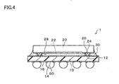
- a semiconductor device 1 shown in FIG. 4 is manufactured in this manner.
- the oxide film 15 adhering to the surface of the electrical connection section 14 can be removed by utilizing the acid contained in the paste 54, the reliability of the subsequent step of providing the solder 58 is improved. Specifically, oxidation of the electrical connection section 14 is prevented without forming a plating film so that formation of a hard and fragile alloy layer due to a plating film is prevented, whereby deterioration of the mechanical reliability of the external terminal can be prevented. Moreover, the solder and the electrical connection section 14 can be reliably electrically connected by preventing oxidation of the surface of the electrical connection section 14. Furthermore, since the oxide film 15 can be removed by performing the application step of the paste 54 and the washing step, the manufacturing process is significantly simplified in comparison with the case of forming a plating film in advance.
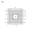
- FIG. 5 is a plan view of the interposer before the external terminal formation step.
- the application step of the paste 54 and the washing step are carried out for a part of the electrical connection sections 14.
- the electrical connection sections 14 are arranged on the interposer 10 in rows and columns.
- the electrical connection sections 14 may be arranged in a quadrilateral configuration.
- the application step of the paste 54 and the washing step are carried out for the electrical connection sections 14 located at positions at which stress tends to be applied to the electrical connection sections 14.
- a plating film for preventing oxidation may be formed on the remaining electrical connection sections 14. This improves the mechanical strength of the area to which stress tends to be applied while ensuring the advantage of forming a plating film (e.g. improvement of temperature cycle reliability).
- the stress used herein includes stress applied due to expansion or shrinkage of the interposer 10 or the semiconductor chip 20.
- the application step of the paste 54 and the washing step may be carried out for (only) electrical connection sections 14a positioned on the outer end (including the outmost end) of the rows and columns, or may be carried out for (only) electrical connection sections 14b positioned at the outer corners of the rows and columns.
- the application step of the paste 54 and the washing step may be carried out for (only) electrical connection sections 14c positioned on the inner end (including the innermost end) closest to the specific area 62, or may be carried out for (only) electrical connection sections 14d positioned at the outer corners of the specific area 62.
- the application step of the paste 54 and the washing step may be carried out for the electrical connection sections 14a (or electrical connection sections 14b) and the electrical connection sections 14c (or electrical connection sections 14d).
- the semiconductor device used in this modification may be a fan-in type semiconductor device, a fan-out type semiconductor device, or a fan-in/out type semiconductor device.
- the electrical connection sections 14 are provided only inside of the mounting area of the semiconductor chip 20.
- the electrical connection sections 14 are provided only outside of the mounting area of the semiconductor chip 20.
- the electrical connection sections 14 are provided inside and outside of the mounting area of the semiconductor chip 20.
- FIGS. 6 to 8 are diagrams showing a method of manufacturing a semiconductor device according to a second embodiment of the invention.
- a semiconductor substrate 120 is provided (see FIG. 6).
- the paste application step and the washing step described in the first embodiment are carried out for an electrode pad (electrical connection section) 124 of the semiconductor substrate 120 to form an external terminal 160 (see FIG. 7).
- the external terminal 160 may be formed of a conductive material such as solder or gold (Au), for example.
- a semiconductor wafer is provided as the semiconductor substrate 120. The semiconductor wafer is cut after the formation step of the external terminal 160 in order to obtain individual semiconductor chips.
- the semiconductor substrate 120 includes an integrated circuit 122 and the electrode pad (e.g. Al pad) 124 electrically connected with the integrated circuit 122.
- the electrode pads 124 are generally positioned on the end (e.g. two or four opposite sides) of each semiconductor chip of the semiconductor wafer.
- a passivation film 128 is formed on the surface of the semiconductor substrate 120 on the side of the electrode pad 124.
- a semiconductor substrate 220 in which electrode pads 224 are formed in the area including the area over an integrated circuit 222 may be provided, and the paste application step and the washing step may be carried out for the electrode pads 224 of the semiconductor substrate 220.
- the electrode pads 224 are arranged in rows and columns over the integrated circuit 222 (over the passivation film 126 in more detail).
- This modification may also be applied to the modification of the first embodiment. Specifically, the paste application step and the washing step may be carried out for only the electrode pads 224 disposed at positions at which stress tends to occur.
- FIGS. 9 to 11 are diagrams showing a method of manufacturing a semiconductor device according to a third embodiment of the invention.
- FIG. 10 is a cross-sectional view along the line X-X shown in FIG. 9.
- a semiconductor substrate 320 in which a redistribution interconnect is formed at a wafer level, is provided (see FIG. 10).
- the paste application step and the washing step described in the first embodiment are carried out for an electrical connection section 332 (e.g. land) of the semiconductor substrate 320 to form an external terminal 360 (see FIG. 11).
- the external terminal 360 may be formed of a conductive material such as solder or gold (Au), for example.
- a semiconductor wafer is provided as the semiconductor substrate 320.
- the semiconductor wafer is cut after the formation step of the external terminal 360 in order to obtain individual semiconductor chips.
- the semiconductor substrate 320 includes an integrated circuit 322 and an electrode pad (e.g. Al pad) 324 electrically connected with the integrated circuit 322.
- the electrode pads 324 are generally positioned on the end (e.g. two or four opposite sides) of each semiconductor chip of the semiconductor wafer.
- a passivation film 326 is formed on the surface of the semiconductor substrate 320 on the side of the electrode pad 324.
- a resin layer 328 is formed on the surface of the semiconductor substrate 320 on the side of the integrated circuit 322.
- the resin layer 328 is an underlayer of the electrical connection section 332 of an interconnect layer 330 described later.
- the resin layer 328 is formed inside the arrangement area of the electrode pads 324, for example.
- a polyimide resin, a silicone-modified polyimide resin, an epoxy resin, a silicone-modified epoxy resin, benzocyclobutene (BCB), polybenzoxazole (PBO), and the like can be given.
- the interconnect layer 330 electrically connected with the electrode pads 324 is formed over the semiconductor substrate 320.
- the interconnect layer 330 is formed from the electrode pad 324 to reach the area over the resin layer 328, and includes the electrical connection section (e.g. land) 332 formed over the resin layer 328.
- the interconnect layer 330 may be formed by stacking one or more layers of copper (Cu), chromium (Cr), titanium (Ti), nickel (Ni), titanium tungsten (TiW), gold (Au), aluminum (Al), nickel vanadium (NiV), and tungsten (W).
- the electrical connection sections 332 may be arranged on the resin layer 328 in rows and columns.
- a resin layer 334 is formed over the semiconductor substrate 320 so that the resin layer 334 covers a part of the interconnect layer 330.
- the resin layer 334 is formed to avoid (at least the center of) the electrical connection section 332 of the interconnect layer 330.
- the resin layer 334 may be a solder resist.
- a resin layer 336 may be formed in the area excluding the top of the external terminal 360 in order to reinforce the base of the external terminal 360.
- the third embodiment may also be applied to the modification of the first embodiment.
- the paste application step and the washing step may be carried out for only the electrical connection sections 332 located at positions at which stress tends to be applied to the electrical connection sections 332.
- FIGS. 12 and 13 are diagrams showing a method of treating an electrical connection section according to a fourth embodiment of the invention.
- the paste application step and the washing step described in the first embodiment are carried out for an electrical connection section 412 (e.g. land) formed on a motherboard 410.
- a protective film 414 e.g. solder resist
- the protective film 414 avoids the electrical connection sections 412.
- the motherboard 410 is a substrate on which an electronic part is mounted.
- a rigid substrate, a flexible substrate, a flexible rigid substrate, a built-up substrate, and the like can be given.
- the electronic parts a semiconductor device, optical element, resistor, capacitor, coil, oscillator, filter, thermosensor, thermistor, varistor, variable resistor, volume, fuse, and the like can be given.
- the semiconductor device 1 as the electronic part may be bonded with solder (soldered) to the electrical connection sections 412 of the motherboard 410 (see FIG. 13).
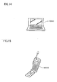
- FIGS. 14 and 15 respectively illustrate a notebook type personal computer 1000 and a portable telephone 2000 as electronic instruments according to a fifth embodiment of the invention.
- the electronic instrument according to the fifth embodiment includes a semiconductor device manufactured according to one of the above-described embodiments.
Landscapes
- Engineering & Computer Science (AREA)
- Manufacturing & Machinery (AREA)
- Microelectronics & Electronic Packaging (AREA)
- Architecture (AREA)
- Civil Engineering (AREA)
- Structural Engineering (AREA)
- Electric Connection Of Electric Components To Printed Circuits (AREA)
- Wire Bonding (AREA)
- Internal Circuitry In Semiconductor Integrated Circuit Devices (AREA)
- Electrodes Of Semiconductors (AREA)
Abstract
Description
- The present invention relates to a method of manufacturing a semiconductor device.
- A solder ball is used as an external terminal of a semiconductor package such as a ball grid array (BGA) or a chip scale package (CSP). A solder ball is provided to an electrical connection section (land) of an interposer of a semiconductor package. An oxidation preventive film such as a plating film is generally formed on the surface of the land. This prevents oxidation of the surface of the land to improve reliability of the step of providing the solder ball. However, this method requires an additional step of treating the plating film. Moreover, when using nickel (Ni) as the material for the plating film, since a hard and fragile alloy layer is formed by soldering, the mechanical reliability of an external terminal may deteriorate.
JP-A-2000-114313 - It is an object of the invention to provide a method of manufacturing a semiconductor device which can improve reliability of an external terminal.
- This object is achieved with a method as claimed in
claim 1. Preferred embodiments of the invention are defined in the dependent claims. - According to the embodiment of the invention, since an oxide film adhering to the surface of the electrical connection section can be removed by the acid contained in the paste, the reliability of the subsequent step of providing the conductive material is improved. Moreover, since the oxide film can be removed by the paste application step and the washing step, the manufacturing process is significantly simplified in comparison with the case of forming a plating film in advance.
- With this method of manufacturing a semiconductor device, the paste applied in the step a) includes a material containing an acid at a ratio higher than that of a material for the flux provided in the step c). This enables the oxide film to be effectively removed from the surface of the electrical connection section.
- With this method of manufacturing a semiconductor device, step a) and step b) may be performed in air or in an oxygen atmosphere. Therefore, even if a gaseous substance adheres to the surface of the electrical connection section during the application step, since the gaseous substance forms an oxide film, the oxide film can be removed by the washing step together with the paste. Therefore, the conductive surface of the electrical connection section can be reliably exposed.
- With this method of manufacturing a semiconductor device, step a) and step b) may be carried out for the electrical connection sections positioned at outer corners of the rows and columns. This is because stress tends to be applied to the corners of the rows and columns in which the electrical connection sections are arranged.
- With this method of manufacturing a semiconductor device, the electrical connection sections may be arranged in rows and columns in an area enclosing a specific area; and step a) and the step b) may be carried out for the electrical connection sections positioned on an inner end of the rows and columns closest to the specific area. This prevents deterioration of the mechanical reliability due to a plating film. Therefore, it is effective to apply this measure to electrical connection sections to which stress tends to be applied.
-
- FIG. 1
- is illustrative of a first embodiment of the invention.
- FIG. 2A
- to FIG. 2C are illustrative of the first embodiment of the invention.
- FIG. 3A
- and FIG. 3B are illustrative of the first embodiment of the invention.
- FIG. 4
- is illustrative of the first embodiment of the invention.
- FIG. 5
- is illustrative of a modification of the first embodiment of the invention.
- FIG. 6
- is illustrative of a second embodiment of the invention.
- FIG. 7
- is illustrative of the second embodiment of the invention.
- FIG. 8
- is illustrative of a modification of the second embodiment of the invention.
- FIG. 9
- is illustrative of a third embodiment of the invention.
- FIG. 10
- is illustrative of the third embodiment of the invention.
- FIG. 11
- is illustrative of the third embodiment of the invention.
- FIG. 12
- is illustrative of a fourth embodiment of the invention.
- FIG. 13
- is illustrative of the fourth embodiment of the invention.
- FIG. 14
- is illustrative of a fifth embodiment of the invention.
- FIG. 15
- is illustrative of the fifth embodiment of the invention.
- The embodiments of the invention are described below with reference to the drawings.
- FIGS. 1 to 4 are diagrams showing a method of manufacturing a semiconductor device according to a first embodiment to which the invention is applied. The method of manufacturing a semiconductor device includes a method of treating an electrical connection section.
- In the first embodiment, an
interposer 10 is provided. A semiconductor chip 20 (semiconductor substrate) is mounted on theinterposer 10. Specifically, in the first embodiment, asemiconductor package 40 is provided by packaging thesemiconductor chip 20. - The
interposer 10 is an interconnect substrate on which thesemiconductor chip 20 is mounted. Theinterposer 10 makes up thesemiconductor package 40. Theinterposer 10 may be an organic resin substrate (e.g. epoxy substrate or polyimide substrate), an inorganic substrate (e.g. glass substrate or ceramic substrate), or an organic and inorganic composite substrate (e.g. glass epoxy substrate). -
Electrical connection sections interposer 10. Theelectrical connection sections electrical connection sections interposer 10. Theprotective film 16 protects the interconnect pattern in the area other than theelectrical connection sections protective film 16 is formed to avoid the center of the electrical connection section 14 (or electrical connection section 12) and to overlap the outer edge of the electrical connection section 14 (or electrical connection section 12). - The
interposer 10 may be a single-layer substrate or a multi-layer substrate. In either case, theelectrical connection sections electrical connection sections - The
semiconductor chip 20 includes anintegrated circuit 22 and an electrode pad 24 (e.g. Al pad) electrically connected with theintegrated circuit 22. Theelectrode pads 24 are generally positioned on the end (e.g. two or four opposite sides) of thesemiconductor chip 20. Apassivation film 28 is formed on the surface of thesemiconductor chip 20 on the side of theelectrode pad 24. - The
semiconductor chip 20 is mounted on the surface of theinterposer 10 on the side of theelectrical connection section 12. Theelectrical connection section 14 is electrically connected with thesemiconductor chip 20 through theelectrical connection section 12. Thesemiconductor chip 20 may be mounted face-down so that the surface on which theelectrode pad 24 is formed faces the interposer, or may be mounted face-up so that the surface on which theelectrode pad 24 is formed faces the direction opposite to the interposer. When mounting thesemiconductor chip 20 face-down, a bump (e.g. Au bump) is generally formed on theelectrode pad 24. In this case, the semiconductor chip 20 (bump) and the interposer 10 (electrical connection section 12) may be electrically connected through an anisotropicconductive material 30. The anisotropicconductive material 30 may be either a film (ACF) or a paste (ACP). The anisotropicconductive material 30 includes a binder and conductive particles dispersed in the binder, and the bump and theelectrical connection section 12 are electrically connected through the conductive particles provided therebetween. Or, thesemiconductor chip 20 and theinterposer 10 may be electrically connected by using a conductive resin paste or a metal junction (e.g. Au-Au junction, Au-Sn junction, or solder junction), or by utilizing the shrinkage force of an insulating resin. When using a metal junction, an underfill material (resin) may be provided between thesemiconductor chip 20 and theinterposer 10. When mounting thesemiconductor chip 20 face-up, thesemiconductor chip 20 and theinterposer 10 are electrically connected by using a wire, and theentire semiconductor chip 20 is generally sealed with a resin. - In the first embodiment, an
external terminal 60 is formed on theelectrical connection section 14 of theinterposer 10, as shown in FIGS. 2A to 4. The method of treating the electrical connection section is described below with reference to FIGS. 2A to 2C. - As shown in FIG. 2A, an
oxide film 15 adheres to the surface of theelectrical connection section 14. Theoxide film 15 is formed due to native oxidation, heating performed in the step of mounting thesemiconductor chip 20, or heating performed in the step of drying theinterposer 10, for example. - A
paste 54 is applied to the electrical connection section 14 (see FIG. 2B). Thepaste 54 contains acid. The acid contained in thepaste 54 may be either an inorganic acid or an organic acid. As the inorganic acid, a halogen acid aqueous solution may be used. As specific examples of the inorganic acid, hydrobromic acid (HBr), hydrochloric acid (HCl), sulfuric acid (H2SO4), nitric acid (HNO3), phosphoric acid (H3PO4), and the like can be given. As a specific example of the organic acid, a carboxylic acid (RCOOH) can be given. Since the inorganic acid has a reducing power higher than that of the organic acid, theoxide film 15 can be effectively removed by using thepaste 54 containing the inorganic acid. It is preferable to use hydrochloric acid or sulfuric acid since the hydrochloric acid or sulfuric acid has a reducing power higher than other inorganic acids (e.g. higher than hydrobromic acid). - The
paste 54 may be flux. In this case, thepaste 54 may contain a resin, an active agent, a solvent, and a thixotropic agent. As the resin, a water-soluble resin or a rosin-based resin may be used. The composition of the flux is not particularly limited insofar as the flux contains acid. For example, the flux may contain an aliphatic glycol ether, a modified hardened castor oil, glyceryl ether, an organic acid, an organic amine halogenated salt, and solder powder at a specific ratio. - The
paste 54 may be formed of a material the same as the material for a soldering flux 56 (see FIG. 3A) described later. This reduces the number of chemicals used in the manufacturing process. Thepaste 54 may be formed of a material containing acid at a ratio higher than that of the material for thesoldering flux 56. Thepaste 54 may be formed of a material containing acid having a higher reducing power than that of the acid contained in thesoldering flux 56. The above measure enables theoxide film 15 to be effectively removed from the surface of theelectrical connection section 14. - The
paste 54 may be applied by using a pin transfer method as shown in FIG. 2A, in which adroplet 52 is transferred by using apin 50. As another method, a printing method (e.g. screen printing method), an inkjet method, an application method using a dispenser, or the like may be used. It suffices that thepaste 54 be applied to theinterposer 10 in the area including theelectrical connection section 14. As shown in FIG. 2B, thepaste 54 may be separately applied in units ofelectrical connection sections 14, for example. - After applying the
paste 54 as shown in FIG. 2B, thepaste 54 is allowed to stand for a specific period of time until a reduction reaction of a metal used as the material for theelectrical connection section 14 is completed. For example, when using copper as the material for theelectrical connection section 14 and applying thepaste 54 containing hydrobromic acid to theelectrical connection section 14, a chemical reaction shown by the following formula occurs. - The
paste 54 may be heated in order to promote the chemical reaction. Or, thepaste 54 may be allowed to stand at room temperature without heating in order to prevent volatilization of the acid contained in thepaste 54. The chemical reaction reliably occurs by preventing volatilization of the acid. - Then, the
paste 54 is removed from theelectrical connection section 14 by washing theelectrical connection section 14, as shown in FIG. 2C. This allows theoxide film 15 adhering to the surface of theelectrical connection section 14 to be removed together with thepaste 54. Specifically, the conductive surface of theelectrical connection section 14 can be reliably exposed. - The application step of the
paste 54 and the washing step may be carried out in air or in an oxygen atmosphere. Therefore, even if a gaseous substance adheres to the surface of theelectrical connection section 14 during the application step, since the gaseous substance forms an oxide film, the oxide film can be removed by the washing step together with thepaste 54. This allows the conductive surface of theelectrical connection section 14 to be reliably exposed. The application step of thepaste 54 and the washing step may be carried out for all theelectrical connection sections 14. - Then, a conductive material is provided on the
electrical connection section 14. When using solder as the conductive material,solder 58 may be provided to theelectrical connection section 14 through theflux 56. Thesolder 58 may be provided to theelectrical connection section 14 as a solid solder ball. Thesoldering flux 56 is provided to improve the wettability of thesolder 58 and to prevent oxidation of the surface of theexternal terminal 60 after completion of the product. Thesoldering flux 56 may be provided to theelectrical connection section 14 before providing thesolder 58. Thesolder 58 contains tin (Sn), for example. - Then, a reflow step is performed to form the
external terminal 60 on theelectrical connection section 14, as shown in FIG. 4. Theflux 56 remaining on theexternal terminal 60 is removed by washing. - When performing the above-described steps for a set of
interposers 10, theinterposers 10 are separated by cutting. Asemiconductor device 1 shown in FIG. 4 is manufactured in this manner. - According to the method of manufacturing a semiconductor device according to the first embodiment, since the
oxide film 15 adhering to the surface of theelectrical connection section 14 can be removed by utilizing the acid contained in thepaste 54, the reliability of the subsequent step of providing thesolder 58 is improved. Specifically, oxidation of theelectrical connection section 14 is prevented without forming a plating film so that formation of a hard and fragile alloy layer due to a plating film is prevented, whereby deterioration of the mechanical reliability of the external terminal can be prevented. Moreover, the solder and theelectrical connection section 14 can be reliably electrically connected by preventing oxidation of the surface of theelectrical connection section 14. Furthermore, since theoxide film 15 can be removed by performing the application step of thepaste 54 and the washing step, the manufacturing process is significantly simplified in comparison with the case of forming a plating film in advance. - A modification of the first embodiment is described below. FIG. 5 is a plan view of the interposer before the external terminal formation step. In this modification, the application step of the
paste 54 and the washing step are carried out for a part of theelectrical connection sections 14. - As shown in FIG. 5, the
electrical connection sections 14 are arranged on theinterposer 10 in rows and columns. For example, theelectrical connection sections 14 may be arranged in a quadrilateral configuration. In this modification, the application step of thepaste 54 and the washing step are carried out for theelectrical connection sections 14 located at positions at which stress tends to be applied to theelectrical connection sections 14. A plating film for preventing oxidation may be formed on the remainingelectrical connection sections 14. This improves the mechanical strength of the area to which stress tends to be applied while ensuring the advantage of forming a plating film (e.g. improvement of temperature cycle reliability). The stress used herein includes stress applied due to expansion or shrinkage of theinterposer 10 or thesemiconductor chip 20. - For example, the application step of the
paste 54 and the washing step may be carried out for (only)electrical connection sections 14a positioned on the outer end (including the outmost end) of the rows and columns, or may be carried out for (only)electrical connection sections 14b positioned at the outer corners of the rows and columns. - As shown in FIG. 5, when the
electrical connection sections 14 are arranged in rows and columns in the area enclosing a specific area 62 (e.g. semiconductor chip mounting area), the application step of thepaste 54 and the washing step may be carried out for (only)electrical connection sections 14c positioned on the inner end (including the innermost end) closest to thespecific area 62, or may be carried out for (only)electrical connection sections 14d positioned at the outer corners of thespecific area 62. The application step of thepaste 54 and the washing step may be carried out for theelectrical connection sections 14a (orelectrical connection sections 14b) and theelectrical connection sections 14c (orelectrical connection sections 14d). - The semiconductor device used in this modification may be a fan-in type semiconductor device, a fan-out type semiconductor device, or a fan-in/out type semiconductor device. In a fan-in type semiconductor device, the
electrical connection sections 14 are provided only inside of the mounting area of thesemiconductor chip 20. In a fan-out type semiconductor device, theelectrical connection sections 14 are provided only outside of the mounting area of thesemiconductor chip 20. In a fan-in/out type semiconductor device, theelectrical connection sections 14 are provided inside and outside of the mounting area of thesemiconductor chip 20. - According to this modification, since deterioration of the mechanical reliability due to a plating film is prevented, it is effective to apply this modification to the
electrical connection sections 14a to 14d to which stress tends to be applied. - FIGS. 6 to 8 are diagrams showing a method of manufacturing a semiconductor device according to a second embodiment of the invention.
- In the second embodiment, a
semiconductor substrate 120 is provided (see FIG. 6). The paste application step and the washing step described in the first embodiment are carried out for an electrode pad (electrical connection section) 124 of thesemiconductor substrate 120 to form an external terminal 160 (see FIG. 7). Theexternal terminal 160 may be formed of a conductive material such as solder or gold (Au), for example. When carrying out the above-described steps for a wafer, a semiconductor wafer is provided as thesemiconductor substrate 120. The semiconductor wafer is cut after the formation step of theexternal terminal 160 in order to obtain individual semiconductor chips. - The
semiconductor substrate 120 includes anintegrated circuit 122 and the electrode pad (e.g. Al pad) 124 electrically connected with theintegrated circuit 122. Theelectrode pads 124 are generally positioned on the end (e.g. two or four opposite sides) of each semiconductor chip of the semiconductor wafer. Apassivation film 128 is formed on the surface of thesemiconductor substrate 120 on the side of theelectrode pad 124. - As a modification of the second embodiment, as shown in FIG. 8, a
semiconductor substrate 220 in which electrodepads 224 are formed in the area including the area over anintegrated circuit 222 may be provided, and the paste application step and the washing step may be carried out for theelectrode pads 224 of thesemiconductor substrate 220. Theelectrode pads 224 are arranged in rows and columns over the integrated circuit 222 (over thepassivation film 126 in more detail). - According to this modification, since the
electrode pads 224 are formed over theintegrated circuit 222, a structure which can endure a larger amount of stress is required. However, such a requirement can be dealt with by applying this modification. - This modification may also be applied to the modification of the first embodiment. Specifically, the paste application step and the washing step may be carried out for only the
electrode pads 224 disposed at positions at which stress tends to occur. - FIGS. 9 to 11 are diagrams showing a method of manufacturing a semiconductor device according to a third embodiment of the invention. FIG. 10 is a cross-sectional view along the line X-X shown in FIG. 9.
- In the third embodiment, a
semiconductor substrate 320, in which a redistribution interconnect is formed at a wafer level, is provided (see FIG. 10). The paste application step and the washing step described in the first embodiment are carried out for an electrical connection section 332 (e.g. land) of thesemiconductor substrate 320 to form an external terminal 360 (see FIG. 11). Theexternal terminal 360 may be formed of a conductive material such as solder or gold (Au), for example. When carrying out the above-described steps for a wafer, a semiconductor wafer is provided as thesemiconductor substrate 320. The semiconductor wafer is cut after the formation step of theexternal terminal 360 in order to obtain individual semiconductor chips. - The
semiconductor substrate 320 includes anintegrated circuit 322 and an electrode pad (e.g. Al pad) 324 electrically connected with theintegrated circuit 322. Theelectrode pads 324 are generally positioned on the end (e.g. two or four opposite sides) of each semiconductor chip of the semiconductor wafer. Apassivation film 326 is formed on the surface of thesemiconductor substrate 320 on the side of theelectrode pad 324. - A
resin layer 328 is formed on the surface of thesemiconductor substrate 320 on the side of theintegrated circuit 322. Theresin layer 328 is an underlayer of theelectrical connection section 332 of aninterconnect layer 330 described later. Theresin layer 328 is formed inside the arrangement area of theelectrode pads 324, for example. As examples of the material for theresin layer 328, a polyimide resin, a silicone-modified polyimide resin, an epoxy resin, a silicone-modified epoxy resin, benzocyclobutene (BCB), polybenzoxazole (PBO), and the like can be given. - The
interconnect layer 330 electrically connected with theelectrode pads 324 is formed over thesemiconductor substrate 320. Theinterconnect layer 330 is formed from theelectrode pad 324 to reach the area over theresin layer 328, and includes the electrical connection section (e.g. land) 332 formed over theresin layer 328. Theinterconnect layer 330 may be formed by stacking one or more layers of copper (Cu), chromium (Cr), titanium (Ti), nickel (Ni), titanium tungsten (TiW), gold (Au), aluminum (Al), nickel vanadium (NiV), and tungsten (W). Theelectrical connection sections 332 may be arranged on theresin layer 328 in rows and columns. - A
resin layer 334 is formed over thesemiconductor substrate 320 so that theresin layer 334 covers a part of theinterconnect layer 330. Theresin layer 334 is formed to avoid (at least the center of) theelectrical connection section 332 of theinterconnect layer 330. Theresin layer 334 may be a solder resist. - As shown in FIG. 11, after forming an
external terminal 360 on theelectrical connection section 332 of thesemiconductor substrate 320, aresin layer 336 may be formed in the area excluding the top of theexternal terminal 360 in order to reinforce the base of theexternal terminal 360. - The third embodiment may also be applied to the modification of the first embodiment. Specifically, the paste application step and the washing step may be carried out for only the
electrical connection sections 332 located at positions at which stress tends to be applied to theelectrical connection sections 332. - FIGS. 12 and 13 are diagrams showing a method of treating an electrical connection section according to a fourth embodiment of the invention.
- In the fourth embodiment, the paste application step and the washing step described in the first embodiment are carried out for an electrical connection section 412 (e.g. land) formed on a
motherboard 410. A protective film 414 (e.g. solder resist) is formed on themotherboard 410 so that theprotective film 414 avoids theelectrical connection sections 412. - The
motherboard 410 is a substrate on which an electronic part is mounted. As examples of themotherboard 410, a rigid substrate, a flexible substrate, a flexible rigid substrate, a built-up substrate, and the like can be given. As examples of the electronic parts, a semiconductor device, optical element, resistor, capacitor, coil, oscillator, filter, thermosensor, thermistor, varistor, variable resistor, volume, fuse, and the like can be given. For example, after performing the paste application step and the washing step, thesemiconductor device 1 as the electronic part may be bonded with solder (soldered) to theelectrical connection sections 412 of the motherboard 410 (see FIG. 13). - Fifth Embodiment
- FIGS. 14 and 15 respectively illustrate a notebook type
personal computer 1000 and aportable telephone 2000 as electronic instruments according to a fifth embodiment of the invention. The electronic instrument according to the fifth embodiment includes a semiconductor device manufactured according to one of the above-described embodiments. - Although only some embodiments of the present invention have been described in detail above, those skilled in the art will readily appreciate that many modifications are possible in the embodiments without materially departing from the novel teachings and advantages of this invention. Accordingly, all such modifications are intended to be included within scope of this invention.
Claims (10)
- A method of manufacturing a semiconductor device, comprising:a) applying a paste containing acid to an electrical connection section which is electrically connected with an integrated circuit included in a semiconductor substrate, the paste including an acid at a first ratio;b) removing the paste from the electrical connection section by washing the electrical connection section; andc) providing a solder to the electrical connection section through a flux, the flux including an acid at a second ratio, the second ratio being lower than the first ratio.
- The method as defined in claim 1, wherein step a) and the step b) are performed in air or in an oxygen atmosphere.
- The method as defined claim 1 or 2, wherein the acid contained in the paste is an organic acid.
- The method as defined in claim 1 or 2, wherein the acid contained in the paste is an inorganic acid.
- The method as defined in any one of claims 1 to 4,
wherein the semiconductor substrate is mounted on an interposer; and
wherein the electrical connection section is a land formed on the interposer. - The semiconductor device as defined in any one of claims 1 to 4, wherein the electrical connection section is an electrode pad formed on the semiconductor substrate.
- The method as defined in any one of claims 1 to 4,
wherein a resin layer is formed on the semiconductor substrate; and
wherein the electrical connection section is a land formed on the resin layer. - The method as defined in any one of claims 1 to 7,
wherein the electrical connection sections are arranged in rows and columns; and
wherein step a) and step b) are carried out for the electrical connection sections positioned on an outer end of the rows and columns. - The method as defined in claim 8,
wherein step a) and step b) are carried out for the electrical connection sections positioned at outer corners of the rows and columns. - The method as defined in claim 8 or 9,
wherein the electrical connection sections are arranged in rows and columns in an area enclosing a specific area; and
wherein step a) and step b) are carried out for the electrical connection sections positioned on an inner end of the rows and columns closest to the specific area.
Applications Claiming Priority (2)
| Application Number | Priority Date | Filing Date | Title |
|---|---|---|---|
| JP2005011763A JP4035733B2 (en) | 2005-01-19 | 2005-01-19 | Manufacturing method of semiconductor device and processing method of electrical connection part |
| EP06001010A EP1684339A3 (en) | 2005-01-19 | 2006-01-18 | Method of manufacturing semiconductor device and method of treating electrical connection section |
Related Parent Applications (1)
| Application Number | Title | Priority Date | Filing Date |
|---|---|---|---|
| EP06001010A Division EP1684339A3 (en) | 2005-01-19 | 2006-01-18 | Method of manufacturing semiconductor device and method of treating electrical connection section |
Publications (2)
| Publication Number | Publication Date |
|---|---|
| EP1858070A2 true EP1858070A2 (en) | 2007-11-21 |
| EP1858070A3 EP1858070A3 (en) | 2008-08-06 |
Family
ID=36263673
Family Applications (2)
| Application Number | Title | Priority Date | Filing Date |
|---|---|---|---|
| EP07017535A Withdrawn EP1858070A3 (en) | 2005-01-19 | 2006-01-18 | Method of manufacturing semiconductor device |
| EP06001010A Withdrawn EP1684339A3 (en) | 2005-01-19 | 2006-01-18 | Method of manufacturing semiconductor device and method of treating electrical connection section |
Family Applications After (1)
| Application Number | Title | Priority Date | Filing Date |
|---|---|---|---|
| EP06001010A Withdrawn EP1684339A3 (en) | 2005-01-19 | 2006-01-18 | Method of manufacturing semiconductor device and method of treating electrical connection section |
Country Status (6)
| Country | Link |
|---|---|
| US (1) | US7608479B2 (en) |
| EP (2) | EP1858070A3 (en) |
| JP (1) | JP4035733B2 (en) |
| KR (1) | KR100687000B1 (en) |
| CN (2) | CN100444343C (en) |
| TW (1) | TWI285931B (en) |
Families Citing this family (14)
| Publication number | Priority date | Publication date | Assignee | Title |
|---|---|---|---|---|
| WO2007052790A1 (en) * | 2005-11-07 | 2007-05-10 | Tyco Electronics Raychem K.K. | Ptc device |
| US20080038913A1 (en) * | 2006-08-10 | 2008-02-14 | International Business Machines Corporation | Methods of forming aluminum-free wire bond pad and pad so formed |
| US20110005822A1 (en) * | 2006-10-20 | 2011-01-13 | Yuuki Momokawa | Structure of a package for electronic devices and method for manufacturing the package |
| KR101044008B1 (en) | 2008-10-08 | 2011-06-24 | 주식회사 하이닉스반도체 | Flexible semiconductor package and manufacturing method thereof |
| TWI458054B (en) * | 2009-01-21 | 2014-10-21 | 新力股份有限公司 | Semiconductor device and method of manufacturing the same |
| US8214696B2 (en) | 2009-02-02 | 2012-07-03 | Lg Electronics Inc. | Apparatus and method for transmitting signal using bit grouping in wireless communication system |
| EP2398046A1 (en) * | 2010-06-18 | 2011-12-21 | Nxp B.V. | Integrated circuit package with a copper-tin joining layer and manufacturing method thereof |
| US20120002386A1 (en) * | 2010-07-01 | 2012-01-05 | Nokia Corporation | Method and Apparatus for Improving the Reliability of Solder Joints |
| CN102366861A (en) * | 2011-06-27 | 2012-03-07 | 吴江市精工铝字制造厂 | Soldering flux for welding aluminum alloy |
| JP2013143542A (en) * | 2012-01-12 | 2013-07-22 | Tokyo Electron Ltd | Semiconductor device manufacturing system and semiconductor device manufacturing method |
| US9728517B2 (en) * | 2013-12-17 | 2017-08-08 | Taiwan Semiconductor Manufacturing Company Ltd. | Semiconductor device and manufacturing method thereof |
| KR101985499B1 (en) * | 2017-12-28 | 2019-06-03 | 삼화콘덴서공업 주식회사 | Over-current protected metal oxide varistor |
| CN110660747A (en) | 2018-06-28 | 2020-01-07 | 晟碟信息科技(上海)有限公司 | Semiconductor device including reinforced corner supports |
| DE112023006195T5 (en) * | 2023-06-23 | 2026-02-26 | Scrona Ag | Pressure-assisted hybrid joining technology |
Family Cites Families (37)
| Publication number | Priority date | Publication date | Assignee | Title |
|---|---|---|---|---|
| US4714517A (en) | 1986-05-08 | 1987-12-22 | National Semiconductor Corporation | Copper cleaning and passivating for tape automated bonding |
| JPH0692034B2 (en) * | 1989-08-23 | 1994-11-16 | ユーホーケミカル株式会社 | Non-cleaning type flux and solder paste |
| US5127968A (en) | 1989-08-16 | 1992-07-07 | Yuho Chemicals Inc. | Additive for fluxes and soldering pastes |
| JPH084953B2 (en) | 1991-04-17 | 1996-01-24 | ユーホーケミカル株式会社 | Corrosion inhibitor for flux or solder paste |
| JPH0763105B2 (en) | 1993-02-12 | 1995-07-05 | 日本電気株式会社 | Method for manufacturing printed wiring board |
| JP3247211B2 (en) | 1993-08-02 | 2002-01-15 | 富士通株式会社 | Copper oxide removal method for copper film surface for wiring |
| US6025258A (en) | 1994-01-20 | 2000-02-15 | Fujitsu Limited | Method for fabricating solder bumps by forming solder balls with a solder ball forming member |
| US6319810B1 (en) | 1994-01-20 | 2001-11-20 | Fujitsu Limited | Method for forming solder bumps |
| US5643831A (en) | 1994-01-20 | 1997-07-01 | Fujitsu Limited | Process for forming solder balls on a plate having apertures using solder paste and transferring the solder balls to semiconductor device |
| US6528346B2 (en) | 1994-01-20 | 2003-03-04 | Fujitsu Limited | Bump-forming method using two plates and electronic device |
| US6271110B1 (en) | 1994-01-20 | 2001-08-07 | Fujitsu Limited | Bump-forming method using two plates and electronic device |
| JP3124224B2 (en) * | 1996-04-01 | 2001-01-15 | 富士通株式会社 | Solder bump formation method |
| DE19733731A1 (en) | 1997-08-04 | 1999-02-25 | Siemens Ag | Integrated electrical circuit with passivation layer |
| JP3896701B2 (en) | 1998-09-29 | 2007-03-22 | ソニー株式会社 | Method for producing solder bump electrode |
| US6358847B1 (en) | 1999-03-31 | 2002-03-19 | Lam Research Corporation | Method for enabling conventional wire bonding to copper-based bond pad features |
| KR20010045222A (en) * | 1999-11-03 | 2001-06-05 | 박종섭 | Method for cleaning bump in semiconductor device |
| JP2001156441A (en) * | 1999-11-29 | 2001-06-08 | Nec Ibaraki Ltd | Repair method for CSP / BGA |
| US6540127B2 (en) * | 2000-06-22 | 2003-04-01 | The Regents Of The University Of California | Electrostatic methods and apparatus for mounting and demounting particles from a surface having an array of tacky and non-tacky areas |
| US6713880B2 (en) * | 2001-02-07 | 2004-03-30 | Matsushita Electric Industrial Co., Ltd. | Semiconductor device and method for producing the same, and method for mounting semiconductor device |
| JP3500378B2 (en) * | 2001-02-07 | 2004-02-23 | 松下電器産業株式会社 | Semiconductor device and manufacturing method thereof |
| US6803650B2 (en) * | 2001-02-23 | 2004-10-12 | Silicon Bandwidth Inc. | Semiconductor die package having mesh power and ground planes |
| US6693020B2 (en) | 2001-03-12 | 2004-02-17 | Motorola, Inc. | Method of preparing copper metallization die for wirebonding |
| US20020180029A1 (en) * | 2001-04-25 | 2002-12-05 | Hideki Higashitani | Semiconductor device with intermediate connector |
| JP3761461B2 (en) * | 2001-12-13 | 2006-03-29 | Necエレクトロニクス株式会社 | Manufacturing method of semiconductor device |
| US20030119295A1 (en) * | 2001-12-24 | 2003-06-26 | Fang-Chu Chang | Wafer and method of fabricating the same |
| JP2003224161A (en) * | 2002-01-30 | 2003-08-08 | Sumitomo Bakelite Co Ltd | Semiconductor package and manufacturing method therefor |
| US6854633B1 (en) | 2002-02-05 | 2005-02-15 | Micron Technology, Inc. | System with polymer masking flux for fabricating external contacts on semiconductor components |
| WO2003075340A2 (en) | 2002-03-01 | 2003-09-12 | Interuniversitair Microelektronica Centrum | Method for obtaining metal to metal contact between a metal surface and a bonding pad. |
| JP2003258155A (en) * | 2002-03-05 | 2003-09-12 | Ngk Spark Plug Co Ltd | Manufacturing method of wiring board |
| JP3802824B2 (en) | 2002-03-05 | 2006-07-26 | 日本特殊陶業株式会社 | Wiring board manufacturing method |
| US6899816B2 (en) * | 2002-04-03 | 2005-05-31 | Applied Materials, Inc. | Electroless deposition method |
| US6720204B2 (en) | 2002-04-11 | 2004-04-13 | Chartered Semiconductor Manufacturing Ltd. | Method of using hydrogen plasma to pre-clean copper surfaces during Cu/Cu or Cu/metal bonding |
| US6818988B2 (en) * | 2002-07-25 | 2004-11-16 | International Business Machines Corporation | Method of making a circuitized substrate and the resultant circuitized substrate |
| JP4120324B2 (en) | 2002-09-12 | 2008-07-16 | 沖電気工業株式会社 | Ball electrode forming method |
| JP3929381B2 (en) * | 2002-10-04 | 2007-06-13 | 株式会社ルネサステクノロジ | Semiconductor device |
| JP3898628B2 (en) * | 2002-11-22 | 2007-03-28 | 日本特殊陶業株式会社 | Wiring board and manufacturing method thereof |
| JP2004207381A (en) | 2002-12-24 | 2004-07-22 | Shinko Electric Ind Co Ltd | Wiring board, method of manufacturing the same, and semiconductor device |
-
2005
- 2005-01-19 JP JP2005011763A patent/JP4035733B2/en not_active Expired - Fee Related
- 2005-12-22 TW TW094145939A patent/TWI285931B/en not_active IP Right Cessation
-
2006
- 2006-01-17 US US11/332,262 patent/US7608479B2/en not_active Expired - Fee Related
- 2006-01-18 EP EP07017535A patent/EP1858070A3/en not_active Withdrawn
- 2006-01-18 EP EP06001010A patent/EP1684339A3/en not_active Withdrawn
- 2006-01-18 KR KR1020060005386A patent/KR100687000B1/en not_active Expired - Fee Related
- 2006-01-19 CN CNB2006100061439A patent/CN100444343C/en not_active Expired - Fee Related
- 2006-01-19 CN CNB2007101860221A patent/CN100570848C/en not_active Expired - Fee Related
Also Published As
| Publication number | Publication date |
|---|---|
| EP1858070A3 (en) | 2008-08-06 |
| KR100687000B1 (en) | 2007-02-26 |
| EP1684339A2 (en) | 2006-07-26 |
| CN1819133A (en) | 2006-08-16 |
| KR20060084386A (en) | 2006-07-24 |
| JP2006202905A (en) | 2006-08-03 |
| TWI285931B (en) | 2007-08-21 |
| CN100570848C (en) | 2009-12-16 |
| US7608479B2 (en) | 2009-10-27 |
| CN101179039A (en) | 2008-05-14 |
| CN100444343C (en) | 2008-12-17 |
| US20060160347A1 (en) | 2006-07-20 |
| EP1684339A3 (en) | 2007-03-14 |
| JP4035733B2 (en) | 2008-01-23 |
| TW200634958A (en) | 2006-10-01 |
Similar Documents
| Publication | Publication Date | Title |
|---|---|---|
| US11894330B2 (en) | Methods of manufacturing a semiconductor device including a joint adjacent to a post | |
| CN102347319B (en) | Package-on-package structure with reduced bump bridging | |
| US7608479B2 (en) | Method of manufacturing semiconductor device and method of treating electrical connection section | |
| US7790501B2 (en) | Semiconductor chip passivation structures and methods of making the same | |
| US8410604B2 (en) | Lead-free structures in a semiconductor device | |
| KR101011840B1 (en) | Semiconductor package and manufacturing method thereof | |
| US20060043603A1 (en) | Low temperature PB-free processing for semiconductor devices | |
| CN101755334A (en) | Semiconductor device | |
| KR20090126762A (en) | Printed circuit board mounted with semiconductor chip and manufacturing method | |
| US20190244925A1 (en) | Semiconductor device | |
| JP2006041401A (en) | Semiconductor device and manufacturing method thereof | |
| US10199345B2 (en) | Method of fabricating substrate structure | |
| US10867944B2 (en) | Semiconductor structure and manufacturing method thereof | |
| JPH11126852A (en) | Semiconductor device, method of manufacturing the same, and method of mounting conductive ball | |
| KR100705757B1 (en) | Flip chip having extremely fine pitch and manufacturing method thereof | |
| US7344971B2 (en) | Manufacturing method of semiconductor device | |
| JP2008047928A (en) | Manufacturing method of semiconductor device and processing method of electrical connection part | |
| CN113451248B (en) | Electronic package, supporting structure thereof and manufacturing method thereof |
Legal Events
| Date | Code | Title | Description |
|---|---|---|---|
| PUAI | Public reference made under article 153(3) epc to a published international application that has entered the european phase |
Free format text: ORIGINAL CODE: 0009012 |
|
| AC | Divisional application: reference to earlier application |
Ref document number: 1684339 Country of ref document: EP Kind code of ref document: P |
|
| AK | Designated contracting states |
Kind code of ref document: A2 Designated state(s): DE FI FR GB IT NL |
|
| PUAL | Search report despatched |
Free format text: ORIGINAL CODE: 0009013 |
|
| AK | Designated contracting states |
Kind code of ref document: A3 Designated state(s): DE FI FR GB IT NL |
|
| AKX | Designation fees paid |
Designated state(s): DE FI FR GB IT NL |
|
| STAA | Information on the status of an ep patent application or granted ep patent |
Free format text: STATUS: THE APPLICATION IS DEEMED TO BE WITHDRAWN |
|
| 18D | Application deemed to be withdrawn |
Effective date: 20090207 |