EP1855432A1 - Modulation circuit and electronic device - Google Patents
Modulation circuit and electronic device Download PDFInfo
- Publication number
- EP1855432A1 EP1855432A1 EP05719659A EP05719659A EP1855432A1 EP 1855432 A1 EP1855432 A1 EP 1855432A1 EP 05719659 A EP05719659 A EP 05719659A EP 05719659 A EP05719659 A EP 05719659A EP 1855432 A1 EP1855432 A1 EP 1855432A1
- Authority
- EP
- European Patent Office
- Prior art keywords
- signal
- maximum value
- multilevel
- multilevel signal
- amplitude
- Prior art date
- Legal status (The legal status is an assumption and is not a legal conclusion. Google has not performed a legal analysis and makes no representation as to the accuracy of the status listed.)
- Granted
Links
Images



Classifications
-
- H—ELECTRICITY
- H04—ELECTRIC COMMUNICATION TECHNIQUE
- H04L—TRANSMISSION OF DIGITAL INFORMATION, e.g. TELEGRAPHIC COMMUNICATION
- H04L27/00—Modulated-carrier systems
- H04L27/02—Amplitude-modulated carrier systems, e.g. using on-off keying; Single sideband or vestigial sideband modulation
- H04L27/06—Demodulator circuits; Receiver circuits
-
- H—ELECTRICITY
- H03—ELECTRONIC CIRCUITRY
- H03K—PULSE TECHNIQUE
- H03K5/00—Manipulating of pulses not covered by one of the other main groups of this subclass
- H03K5/01—Shaping pulses
- H03K5/08—Shaping pulses by limiting; by thresholding; by slicing, i.e. combined limiting and thresholding
- H03K5/082—Shaping pulses by limiting; by thresholding; by slicing, i.e. combined limiting and thresholding with an adaptive threshold
-
- H—ELECTRICITY
- H03—ELECTRONIC CIRCUITRY
- H03K—PULSE TECHNIQUE
- H03K9/00—Demodulating pulses which have been modulated with a continuously-variable signal
- H03K9/02—Demodulating pulses which have been modulated with a continuously-variable signal of amplitude-modulated pulses
-
- H—ELECTRICITY
- H04—ELECTRIC COMMUNICATION TECHNIQUE
- H04L—TRANSMISSION OF DIGITAL INFORMATION, e.g. TELEGRAPHIC COMMUNICATION
- H04L25/00—Baseband systems
- H04L25/02—Details ; arrangements for supplying electrical power along data transmission lines
- H04L25/06—DC level restoring means; Bias distortion correction ; Decision circuits providing symbol by symbol detection
- H04L25/061—DC level restoring means; Bias distortion correction ; Decision circuits providing symbol by symbol detection providing hard decisions only; arrangements for tracking or suppressing unwanted low frequency components, e.g. removal of DC offset
- H04L25/062—Setting decision thresholds using feedforward techniques only
-
- H—ELECTRICITY
- H04—ELECTRIC COMMUNICATION TECHNIQUE
- H04L—TRANSMISSION OF DIGITAL INFORMATION, e.g. TELEGRAPHIC COMMUNICATION
- H04L25/00—Baseband systems
- H04L25/38—Synchronous or start-stop systems, e.g. for Baudot code
- H04L25/40—Transmitting circuits; Receiving circuits
- H04L25/49—Transmitting circuits; Receiving circuits using code conversion at the transmitter; using predistortion; using insertion of idle bits for obtaining a desired frequency spectrum; using three or more amplitude levels ; Baseband coding techniques specific to data transmission systems
- H04L25/4917—Transmitting circuits; Receiving circuits using code conversion at the transmitter; using predistortion; using insertion of idle bits for obtaining a desired frequency spectrum; using three or more amplitude levels ; Baseband coding techniques specific to data transmission systems using multilevel codes
-
- H—ELECTRICITY
- H04—ELECTRIC COMMUNICATION TECHNIQUE
- H04L—TRANSMISSION OF DIGITAL INFORMATION, e.g. TELEGRAPHIC COMMUNICATION
- H04L27/00—Modulated-carrier systems
- H04L27/02—Amplitude-modulated carrier systems, e.g. using on-off keying; Single sideband or vestigial sideband modulation
- H04L27/08—Amplitude regulation arrangements
-
- H—ELECTRICITY
- H04—ELECTRIC COMMUNICATION TECHNIQUE
- H04L—TRANSMISSION OF DIGITAL INFORMATION, e.g. TELEGRAPHIC COMMUNICATION
- H04L7/00—Arrangements for synchronising receiver with transmitter
- H04L7/0054—Detection of the synchronisation error by features other than the received signal transition
-
- H—ELECTRICITY
- H04—ELECTRIC COMMUNICATION TECHNIQUE
- H04L—TRANSMISSION OF DIGITAL INFORMATION, e.g. TELEGRAPHIC COMMUNICATION
- H04L7/00—Arrangements for synchronising receiver with transmitter
- H04L7/0054—Detection of the synchronisation error by features other than the received signal transition
- H04L7/0062—Detection of the synchronisation error by features other than the received signal transition detection of error based on data decision error, e.g. Mueller type detection
Definitions
- This invention relates to a demodulation circuit and an electronic device, and more particularly, to a demodulation circuit for demodulating multilevel signals received on radio and an electronic device for receiving on radio and demodulating multilevel signals.
- Non-contact data carriers including non-contact IC cards and non-contact ID chips, which do not contain power sources such as batteries, obtain electric power from radio wave energy emitted from reader/writer devices, and at the same time perform data communication by using the radio waves. Therefore, the non-contact data carriers and the reader/writer devices have modulation circuits for modulating data and demodulation circuits for demodulating data.
- the demodulation circuits installed in the non-contact data carriers and the reader/writer devices calculate from a received signal a threshold to be used for determining whether the received signal is H level or L level. Based on the threshold, the demodulation circuits obtain prescribed received data from the received signal.
- FIG. 10 is a view showing circuit blocks of a demodulation circuit to be used in a non-contact data carrier.
- the demodulation circuit has a wave detector 101, a maximum/minimum detector 102, an intermediate value calculator 103, and a comparator 104.
- the wave detector 101 detects a radio signal RF received by an antenna.
- the radio signal RF received by the antenna has been subjected to ASK modulation, for example.
- ASK modulation for example.
- the maximum/minimum detector 102 detects the maximum value and the minimum value of the signal received from the wave detector 101.
- the intermediate value calculator 103 calculates a threshold to be used for determining whether the received radio signal RF is H level or L level, from the maximum value and the minimum value detected by the maximum/minimum detector 102. For example, a threshold is calculated by adding the maximum value and the minimum value and dividing the result by two.
- the comparator 104 detects L state and H state depending on whether the signal received from the wave detector 101 is greater than the threshold calculated by the intermediate value calculator 103. Then, the received data D0 of the detected L state and H state is output to a circuit of latter stage.
- Patent Literature 1 JP 10-261940 A
- This invention has been made in view of foregoing and intends to provide a demodulation circuit and an electronic device that are capable of demodulating multilevel signals to receive many data, without increasing a transfer speed.
- this invention proposes a demodulation circuit for restoring multilevel signals received on radio, as shown in FIG. 1.
- This demodulation circuit comprises an amplitude detector 12 for detecting the maximum value and the minimum value of the amplitude of a multilevel signal, a threshold calculator 13 for calculating a plurality of thresholds to be used for determining whether the multilevel signal is H state or L state, from the maximum value and the minimum value, and a multilevel restoration unit 14 for comparing the multilevel signal with each threshold to detect the H state and the L state and reconstructing a plurality of received data D0 to Dn.
- thresholds to be used for reconstructing received data D0 to Dn are calculated from the maximum value and the minimum value of a multilevel signal, the multilevel signal and the threshold voltages are compared, and the received data D0 and D1 are reconstructed.
- thresholds to be used for reconstructing received data are calculated from the maximum value and the minimum value of a multilevel signal, the multilevel signal and the threshold voltages are compared, and the received data is reconstructed. Therefore, many data can be received without increasing a transfer speed.
- FIG. 1 is a block diagram of a configuration of a demodulation circuit according to the first embodiment.
- the demodulation circuit comprises a wave detector 1, an amplitude detector 12, a threshold calculator 13, and a multilevel restoration unit 14.
- the illustrated demodulation circuit is installed in a non-contact data carrier such as a non-contact IC card or a non-contact ID chip, or a reader/writer device, and is designed to demodulate received multilevel signals transmitted on radio.
- the wave detector 11 detects a radio signal RF received by an antenna.
- the radio signal RF received by the antenna has been subjected to ASK modulation, for example, and by getting the radio signal RF through a lowpass filter or the like, an envelope (multilevel signal) that is a basis of received data D0 to Dn is obtained.
- the wave detector 11 outputs the multilevel signal as electric current or voltage to the amplitude detector 12 and the multilevel restoration unit 14. In the following description, it is assumed that the wave detector 11 outputs the multilevel signal as electric current.
- FIG. 2 is a view showing a multilevel signal output from the wave detector. As shown in this figure, the multilevel signal continues its peak current before signal transmission starts. Then, the signal becomes a signal including information. It is assumed that the multilevel signal has a positive current value.
- the amplitude detector 12 detects the maximum value and the minimum value of the amplitude of the multilevel signal received from the wave detector 11.
- the threshold calculator 13 calculates thresholds to be used for reconstructing received data from the multilevel signal, from the maximum value and the minimum value of the amplitude of the multilevel signal detected by the amplitude detector 12. For example, in the case where the multilevel signal is an N-level signal, thresholds are calculated from the maximum value and the minimum value so that the amplitude of the multilevel signal is divided into N (N is a positive integral number of three or greater).
- the multilevel restoration unit 14 compares the multilevel signal received from the wave detector 11 with each threshold received from the threshold calculator 13. Then, depending on whether the electric current of the multilevel signal is the threshold or greater, information indicating H state or L state is obtained from the multilevel signal, and the received data D0, D1, ..., Dn included in the multilevel signal is reconstructed.
- FIG. 3 is views for explaining how to reconstruct received data from a multilevel signal.
- the figure (A) shows the waveform of a three-level signal (hereinafter, the three-level signal is used for this explanation) output from the wave detector 11. As shown in this figure, in the case of three-level signal, there is an intermediate level in addition to levels corresponding H state and L state.
- the figures (B) and (C) show received data D0 and D1 output from the multilevel restoration unit 14.
- the amplitude detector 12 detects the maximum value and the minimum value of the amplitude of the multilevel signal shown in the figure (A).
- the threshold calculator 13 calculates a center of the amplitude from the maximum value and the minimum value of the amplitude of the multilevel signal detected by the amplitude detector 12. Then a center between the center of the amplitude and the maximum value of the amplitude is calculated to thereby calculate a threshold IthA. In addition, a center between the center of the amplitude and the minimum value of the amplitude is calculated to thereby calculate a threshold IthB. That is, the thresholds are calculated so that the amplitude of the multilevel signal is divided into three with the thresholds IthA and IthB as boarders. In the case of an N-level signal, its amplitude is divided in the same way to thereby obtain N-1 thresholds.
- the multilevel restoration unit 14 compares the threshold IthA received from the threshold calculator 13 with the multilevel signal and outputs the received data D0 shown in the figure (B). For example, if the electric current of the multilevel signal is greater than the threshold IthA, the multilevel signal is identified as being H state, and if the electric current of the multilevel signal is smaller than the threshold IthA, the multilevel signal is identified as being L state, with the result that the received data D0 shown in the figure (B) is output. In addition, the multilevel restoration unit 14 compares the threshold IthB received from the threshold calculator 13 with the multilevel signal, and outputs the received data D1 shown in the figure (C).
- the multilevel signal is identified as being H state, and if the electric current of the multilevel signal is smaller than the threshold IthB, the multilevel signal is identified as being L state, with the result that the received data D1 shown in the figure (C) is output.
- the thresholds to be used for reconstructing received data are calculated from the maximum value and the minimum value of the multilevel signal, and the multilevel signal is compared with the threshold voltages, to thereby reconstruct received data. Therefore, many data can be received without increasing a transfer speed.
- thresholds are dynamically calculated from the maximum value and the minimum value of the multilevel signal, so that, even if a modulation rate of an radio signal RF input to the wave detector 11 varies, stable demodulation can be performed.
- a multilevel signal may be a signal obtained by modulating Manchester codes.
- a multilevel signal is made to have an amplitude of binary, a maximum value and a minimum value, the minimum value is obtained from this binarized multilevel signal, and thresholds are calculated.
- FIG. 4 is a block diagram of a configuration of a demodulation circuit according to the second embodiment.
- the demodulation circuit comprises a wave detector 21, a maximum value detector/holding unit 22, an amplitude binarization unit 23, a minimum value detector/holding unit 24, a threshold calculator 25, a multilevel restoration unit 26, and a sampling timing generator 27.
- the wave detector 21 obtains a multilevel signal from a radio signal RF received by an antenna, as in the wave detector 11 described with FIG. 1.
- the multilevel signal is output to the maximum value detector/holding unit 22, the amplitude binarization unit 23, and the multilevel restoration unit 26.
- the maximum value detector/holding unit 22 detects and holds the maximum value of the electric current of the multilevel signal received from the wave detector 21.
- the maximum value detector/holding unit 22 outputs the held maximum value of the electric current of the multilevel signal to the threshold calculator 25.
- the amplitude binarization unit 23 causes the amplitude of the multilevel signal received from the wave detector 21 to have the maximum value and the minimum value alternately. For example, even if a multilevel signal (here, a three-level signal) of intermediate level is output, a level corresponding to the maximum value and a level corresponding to the minimum value are alternately output. In addition, even if the multilevel signal continues its maximum value, the maximum value level and the minimum value level are always output alternately.
- the amplitude binarization unit 23 receives received data D0 and D1 from the multilevel restoration unit 26, and depending on the H state and L state of the received data D0 and D1, recognizes that the multilevel signal output from the wave detector 21 is intermediate level, and also recognizes that the multilevel signal output from the wave detector 21 continues its maximum value.
- the minimum value detector/holding unit 24 detects and holds the minimum value of the electric current of the multilevel signal received from the amplitude binarization unit 23.
- the minimum value detector/holding unit 24 outputs the held minimum value of the multilevel signal to the threshold calculator 25.
- the minimum value detector/holding unit 24 holds the minimum value of the electric current of the binarized multilevel signal received from the amplitude binarization unit 23, in accordance with a timing signal coming from the sampling timing generator 27 that will be described later.
- the threshold calculator 25 calculates thresholds to be used for reconstructing received data D0 and D1 from the multilevel signal, from the maximum value of the amplitude of the multilevel signal received from the maximum value detector/holding unit 22 and the minimum value of the amplitude of the multilevel signal received from the minimum value detector/holding unit 24, as in the threshold calculator 13 described with FIG. 1.
- the multilevel restoration unit 26 compares the multilevel signal received from the wave detector 11 with each threshold received from the threshold calculator 13, as in the multilevel restoration unit 14 described with FIG. 1. Then the multilevel restoration unit 26 obtains information indicating H state and L state, included in the multilevel signal, depending on whether the electric current of the multilevel signal is greater than the thresholds, and reconstructs the received data D0 and D1 included in the multilevel signal.
- the sampling timing generator 27 receives the received data D0 from the multilevel restoration unit 26.
- the sampling timing generator 27 generates a timing signal of a fixed period based on the received data D0.
- FIG. 5 is views for explaining how to reconstruct received data from a multilevel signal.
- a waveform W11 of the figure (A) is a waveform of a three-level signal output from the wave detector 21. In the case of three-level signal, there is an intermediate level in addition to levels corresponding to H state and L state, as shown in this figure.
- a waveform W12 of the figure (A) shows the maximum value of the amplitude of the multilevel signal. That is, the maximum value detector/holding unit 22 holds the electric current value shown by the waveform W12, and outputs the same to the threshold calculator 25.
- the figure (B) shows a waveform obtained by binarizing the waveform W11 of the figure (A) into an amplitude of the maximum value and the minimum value.
- the figure (B) shows the electric current value that is output from the amplitude binarization unit 23.
- the figure (C) shows the minimum current value of the multilevel signal held by the minimum value detector/holding unit 24.
- the figure (D) shows received data D0 output from the multilevel restoration unit 26.
- the figure (E) shows received data D1 output from the multilevel restoration unit 26.
- the figure (F) shows a timing signal output from the sampling timing generator 27.
- the maximum value detector/holding unit 22 holds the maximum value of the multilevel signal received from the wave detector 21, which is shown by the waveform W12 of the figure (A), and outputs the same to the threshold calculator 25.
- the amplitude binarization unit 23 binarizes the multilevel signal that outputs intermediate level and H state continuously, as shown in the figure (B), and outputs the resultant to the minimum value detector/holding unit 24.
- the amplitude binarization unit 23 recognizes that the multilevel signal is intermediate level, and in this case, it causes the multilevel signal to have the minimum value.
- the amplitude binarization unit 23 recognizes that the multilevel signal continues its H state, and in this case, it causes the multilevel signal to have the minimum value so as not to continue the H state.
- a difference between the maximum value and the intermediate level is calculated, and a doubled value of the difference is subtracted from the maximum value, thereby calculating the minimum value, for example.
- the maximum value is multiplied by a predetermined value (one or smaller), thereby calculating the minimum value, for example.
- the minimum value detector/holding unit 24 holds the minimum value of the binarized multilevel signal, which is shown in the figure (C), and outputs the same to the threshold calculator 25, in accordance with a timing signal coming from the sampling timing generator 27 shown in the figure (F).
- the threshold calculator 25 calculates thresholds IthA and IthB shown in the figure (A), from the maximum value of the amplitude of the multilevel signal received from the maximum value detector/holding unit 22 and the minimum value of the amplitude of the multilevel signal received from the minimum value detector/holding unit 24.
- the multilevel restoration unit 26 compares the threshold IthA received from the threshold calculator 25 with the multilevel signal, and outputs the received data D1 shown in the figure (D). In addition, the multilevel restoration unit 26 compares the threshold IthB received from the threshold calculator 25 with the multilevel signal, and outputs the received data D0 shown in the figure (E).
- the sampling timing generator 27 has a counter, and when a prescribed number is counted after the received data D0 falls, outputs a timing signal of pulse width much smaller than the pulse width of the received data D0, which is shown in the figure (F). If the received data D0 continues its H state, the sampling timing generator 27 periodically outputs a timing signal with reference to a last count value.
- the multilevel signal is binarized to accurately obtain the minimum value of the multilevel signal, so that the received data D0 and D1 can be reconstructed. Therefore, many data can be completely received without increasing a transfer speed.
- the electric current of a multilevel signal output from a wave detector is made to have a minimum value of zero, thereby simplifying signal processing of a circuit.
- FIG. 6 is a block diagram of a configuration of a demodulation circuit according to the third embodiment.
- the demodulation circuit comprises a wave detector 31, a maximum value detector/holding unit 32, a differentiation unit 33, an amplitude binarization unit 34, a maximum value detector/holding unit 35, a threshold calculator 36, a multilevel restoration unit 37, and a sampling timing generator 38.
- the wave detector 31 obtains a multilevel signal from a radio signal RF received by an antenna, as in the wave detector 11 described with FIG. 1.
- the multilevel signal is output to the maximum value detector/holding unit 32 and the differentiation unit 33.
- the maximum value detector/holding unit 32 detects and holds the maximum value of the electric current of the multilevel signal received from the wave detector 31.
- the maximum value detector/holding unit 32 outputs the held maximum value of the electric current of the multilevel signal to the differentiation unit 33.
- the differentiation unit 33 subtracts the multilevel signal received from the wave detector 31 from the maximum value of the electric current of the multilevel signal held by the maximum value detector/holding unit 32, and outputs the resultant.
- the multilevel signal to be output from the differentiation unit 33 is a reversed signal of the multilevel signal and has a minimum current value of zero.
- the reversed multilevel signal from the differentiation unit 33 is output to the amplitude binarization unit 34 and the multilevel restoration unit 37.
- the amplitude binarization unit 34 binarizes the reversed multilevel signal received from the differentiation unit 33, based on the received data D0 and D1 received from the multilevel restoration unit 37, as in the amplitude binarization unit 23 of FIG. 4. That is, even if the multilevel signal (a three-level signal is used for this explanation) of intermediate level is output, the amplitude binarization unit 34 always outputs a level corresponding to H state and a level corresponding to L state alternately. In addition, even if the multilevel signal continues its minimum value, the amplitude binarization unit 34 always outputs the maximum value level and the minimum value level alternately.
- the maximum value detector/holding unit 35 detects and holds the maximum value of the multilevel signal received from the amplitude binarization unit 34.
- the multilevel signal has been reversed by the differentiation unit 33 and its electric current of minimum level is zero, as described above, so that the maximum value is to be held here.
- the maximum value detector/holding unit 35 holds the maximum value of the electric current of the binarized multilevel signal received from the amplitude binarization unit 34, in accordance with a timing signal coming from the sampling timing generator 38 that will be described later.
- the threshold calculator 36 calculates thresholds to be used for reconstructing received data D0 and D1 from a multilevel signal, from the maximum value of the amplitude of the multilevel signal received from the maximum value detector/holding unit 35, as in the threshold calculator 13 described with FIG. 1. It should be noted that the amplitude of the multilevel signal has been made to have a minimum value of zero by the differentiation unit 33.
- the multilevel restoration unit 37 compares the multilevel signal reversed by the differentiation unit 33 with each threshold received from the threshold calculator 36. Then the multilevel restoration unit 37 obtains information indicating H state and L state, included in the multilevel signal, depending on whether the electric current of the multilevel signal output from the differentiation unit 33 is greater than the thresholds, and reconstructs the received data D0 and D1 included in the multilevel signal.
- the sampling timing generator 38 generates a timing signal of a fixed period based on the received data D0, as in the sampling timing generator 27 described with FIG. 4.
- the timing signal is output to the maximum value detector/holding unit 35.
- FIG. 7 is views for explaining how to reconstruct received data from a multilevel signal.
- a waveform W21 of the figure (A) is a waveform of a three-level signal output from the wave detector 21. In the case of three-level signal, there is an intermediate level in addition to levels corresponding to H state and L state, as shown in this figure.
- a waveform W22 of the figure (A) shows the maximum value of the amplitude of the multilevel signal. That is, the maximum value detector/holding unit 32 holds the electric current value shown by the waveform W22 and outputs the same to the differentiation unit 33.
- the figure (B) shows electric current output from the differentiation unit 33.
- the differentiation unit 33 outputs the electric current obtained by subtracting the multilevel signal from the maximum value output from the maximum value detector/holding unit 32, in which the electric current has a minimum value of zero and is a reversed signal of the multilevel signal, as shown in this figure.
- the figure (C) shows a binarized multilevel signal output from the amplitude binarization unit 34.
- the figure (D) shows zero that is the minimum current value of the binarized multilevel signal and the maximum current Imax held by the maximum value detector/holding unit 35.
- the figure (E) shows received data D0 output from the multilevel restoration unit 37.
- the figure (F) shows received data D1 output from the multilevel restoration unit 37.
- the figure (G) shows a timing signal output from the sampling timing generator 38.
- the maximum value detector/holding unit 32 holds the maximum value of the multilelvel signal received from the wave detector 31, which is shown by the waveform W22 of the figure (A), and outputs it to the differentiation unit 33.
- the differentiation unit 33 subtracts the multilevel signal from the maximum value held by the maximum value detector/holding unit 32, and outputs a multilevel signal which has a minimum value of zero and has a reversed waveform, which is shown in the figure (B).
- the amplitude binarization unit 34 binarizes the multilevel signal received from the differentiation unit 33, and outputs the resultant to the maximum value detector/holding unit 35, which is shown in the figure (C).
- a doubled value of the intermediate level is taken as the maximum value, for example.
- a predetermined value is added to the minimum value and its result is taken as the maximum value, for example.
- the maximum value detector/holding unit 35 holds the maximum value (electric current Imax) of the binarized multilevel signal, which is shown in the figure (D), and outputs it to the threshold calculator 36, in accordance with the timing signal coming from the sampling timing generator 38 shown in the figure (G).
- the threshold calculator 36 calculates thresholds IthA and IthB, which are shown in the figure (A), from the maximum value of the amplitude of the multilevel signal received from the maximum value detector/holding unit 35. It should be noted that, since it is known that the minimum value of the amplitude is zero, the thresholds IthA and IthB can be easily calculated only from the maximum value of the amplitude.
- the multilelvel restoration unit 37 compares the threshold IthA received from the threshold calculator 36 with the multilevel signal, and outputs the received data D0 shown in the figure (E). In addition, the multilevel restoration unit 37 compares the threshold IthB received from the threshold calculator 36 with the multilevel signal, and outputs the received data D1 shown in the figure (F).
- the minimum value of the multilevel signal that is, a standard level is set to 0, so that the signal processing to be performed by a circuit of latter stage can be simplified.
- the setting of the standard level to zero decreases power consumption.
- an initial threshold to be used for reconstructing received data from a multilevel signal is determined, and for example, a threshold calculator reconstructs received data by using the initial threshold when the demodulation circuit starts to operate.
- FIG. 8 is a block diagram of a configuration of a demodulation circuit according to the fourth embodiment.
- the same reference numerals as FIG. 4 are given to the same components of FIG. 8 and explanation of them will be omitted.
- a multilevel signal output from a wave detector 21 continues its peak current before signal transmission starts, as described with FIG. 2. Then the signal becomes a signal including information.
- An initial threshold determination unit 41 calculates an initial threshold based on the first peak current, and outputs it to the threshold calculator 42.
- the initial threshold determination unit 41 sets predetermined times peak current as a threshold.
- a threshold can be determined by multiplying the peak current by 0.85. That is, a value greater than an electric current value obtained by multiplying the peak current by 0.85 indicates H state, while a value equal to or lower than the electric current value indicates L state.
- an initial threshold can be determined from the peak current.
- the threshold calculator 42 outputs the threshold calculated by the initial threshold determination unit 41 to the multilevel restoration unit 26 when the signal transmission starts. Then the signal transmission starts and when a multilevel signal including information indicating H state and L state is output, the threshold calculator 42 calculates thresholds to be used for reconstructing received data D0 and D1 from the multilevel signal, from the maximum value and the minimum value of the amplitude of the multilevel signal received from the maximum value detector/holding unit 22 and the minimum value detector/holding unit 24, in the same way described with FIG. 4.
- the minimum value detector/holding unit 24 detects and holds the minimum value of the binarized multilevel signal. Noise superimposed on the multilevel signal may have an influence on the minimum value to be held. For this case, this fifth embodiment enables decrease of an influence of noise on the minimum value.
- another function is added to the minimum value detector/holding unit 24 of FIG. 4 and the other components are identical. Therefore, a block diagram of a configuration is not provided and its description is made with reference to FIG. 4.
- a minimum value detector/holding unit 24 is designed to output 50% of a change in minimum value of the multilevel signal, the minimum value varying due to noise. That is, the minimum value detector/holding unit 24 multiplies the change in the minimum value of the multilevel signal caused by the noise (change between a previous minimum value and a current minimum value) by a coefficient (a value of one or lower), to thereby suppress the influence of the noise.
- FIG. 9 is views for explaining how to reconstruct received data from a multilevel signal.
- the figure (A) shows a waveform of a three-level signal output from the wave detector 21 of FIG. 4.
- the figure (B) shows a waveform obtained by binarizing the multilevel signal of the figure (A) into an amplitude of a maximum value and a minimum value. That is, this figure shows the electric current value that is output from an amplitude binarization unit 23. Since the minimum value of the multilevel signal varies due to noise as described above, the minimum value of the binarized multilevel signal varies as well.
- the figure (C) shows the minimum value held and output by the minimum value detector/holding unit 24.
- the minimum value detector/holding unit 24 of the fifth embodiment outputs 50% of a change in minimum value of the binarized multilevel signal. For example, 50% of a change between the minimum values M11 and M12 shown in the figure (B) is output as shown in the figure (C). In addition, 50% of a change between the minimum values M12 and M13 is output as shown in the figure (C).
- the figure (D) shows received data D0 output from a multilevel restoration unit 26.
- the figure (E) shows received data D1 output from the multilevel restoration unit 26.
- the figure (F) shows a timing signal output from a sampling timing generator 27.
- the above noise suppression can be applied to the third embodiment. That is, similarly to the above minimum value detector/holding unit 24, the maximum value detector/holding unit 35 of FIG. 6 may multiply a change in maximum value of a multilevel signal which is caused due to noise, by a coefficient, thereby suppressing an influence of the noise.
Landscapes
- Engineering & Computer Science (AREA)
- Computer Networks & Wireless Communication (AREA)
- Signal Processing (AREA)
- Physics & Mathematics (AREA)
- Nonlinear Science (AREA)
- Spectroscopy & Molecular Physics (AREA)
- Power Engineering (AREA)
- Dc Digital Transmission (AREA)
- Digital Transmission Methods That Use Modulated Carrier Waves (AREA)
Abstract
Description
- This invention relates to a demodulation circuit and an electronic device, and more particularly, to a demodulation circuit for demodulating multilevel signals received on radio and an electronic device for receiving on radio and demodulating multilevel signals.
- Non-contact data carriers including non-contact IC cards and non-contact ID chips, which do not contain power sources such as batteries, obtain electric power from radio wave energy emitted from reader/writer devices, and at the same time perform data communication by using the radio waves. Therefore, the non-contact data carriers and the reader/writer devices have modulation circuits for modulating data and demodulation circuits for demodulating data.
- The demodulation circuits installed in the non-contact data carriers and the reader/writer devices calculate from a received signal a threshold to be used for determining whether the received signal is H level or L level. Based on the threshold, the demodulation circuits obtain prescribed received data from the received signal.
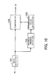
- FIG. 10 is a view showing circuit blocks of a demodulation circuit to be used in a non-contact data carrier. As shown in this figure, the demodulation circuit has a
wave detector 101, a maximum/minimum detector 102, anintermediate value calculator 103, and acomparator 104. - The
wave detector 101 detects a radio signal RF received by an antenna. The radio signal RF received by the antenna has been subjected to ASK modulation, for example. By getting the radio signal RF through a lowpass filter or the like, an envelope that is a basis of received data D0 is obtained. The maximum/minimum detector 102 detects the maximum value and the minimum value of the signal received from thewave detector 101. Theintermediate value calculator 103 calculates a threshold to be used for determining whether the received radio signal RF is H level or L level, from the maximum value and the minimum value detected by the maximum/minimum detector 102. For example, a threshold is calculated by adding the maximum value and the minimum value and dividing the result by two. Thecomparator 104 detects L state and H state depending on whether the signal received from thewave detector 101 is greater than the threshold calculated by theintermediate value calculator 103. Then, the received data D0 of the detected L state and H state is output to a circuit of latter stage. - It should be noted that there exists an automatic threshold value control circuit for always playing digital signals completely, irrespective of amplitude fluctuation and fluctuation of direct current level of signals. (For example, refer to Patent Literature 1).
Patent Literature 1:JP 10-261940 A - By the way, in order to transmit and receive many data, a data transfer speed should be set high. However, a high transfer speed causes spurious, which in turn affects other electronic devices. Therefore, there is a demand for demodulation circuits capable of receiving many data without increasing a transfer speed.
- This invention has been made in view of foregoing and intends to provide a demodulation circuit and an electronic device that are capable of demodulating multilevel signals to receive many data, without increasing a transfer speed.
- In order to solve the above problems, this invention proposes a demodulation circuit for restoring multilevel signals received on radio, as shown in FIG. 1. This demodulation circuit comprises an
amplitude detector 12 for detecting the maximum value and the minimum value of the amplitude of a multilevel signal, athreshold calculator 13 for calculating a plurality of thresholds to be used for determining whether the multilevel signal is H state or L state, from the maximum value and the minimum value, and amultilevel restoration unit 14 for comparing the multilevel signal with each threshold to detect the H state and the L state and reconstructing a plurality of received data D0 to Dn. - According to such a demodulation circuit, thresholds to be used for reconstructing received data D0 to Dn are calculated from the maximum value and the minimum value of a multilevel signal, the multilevel signal and the threshold voltages are compared, and the received data D0 and D1 are reconstructed.
- According to the demodulation circuit of this invention, thresholds to be used for reconstructing received data are calculated from the maximum value and the minimum value of a multilevel signal, the multilevel signal and the threshold voltages are compared, and the received data is reconstructed. Therefore, many data can be received without increasing a transfer speed.
- The above and other objects, features and advantages of the present invention will become apparent from the following description when taken in conjunction with the accompanying drawings which illustrate preferred embodiments of the present invention by way of example.
-
- [FIG. 1] A block diagram of a configuration of a demodulation circuit according to the first embodiment.
- [FIG. 2] A view showing a multilevel signal output from a wave detector.
- [FIG. 3] Views for explaining how to reconstruct received data from a multilevel signal.
- [FIG. 4] A block diagram of a configuration of a demodulation circuit according to the second embodiment.
- [FIG. 5] Views for explaining how to reconstruct received data from a multilevel signal.
- [FIG. 6] A block diagram of a configuration of a demodulation circuit according to the third embodiment.
- [FIG. 7] Views for explaining how to reconstruct received data from a multilevel signal.
- [FIG. 8] A block diagram of a configuration of a demodulation circuit according to the fourth embodiment.
- [FIG. 9] Views for explaining how to reconstruct received data from a multilevel signal.
- [FIG. 10] A view showing circuit blocks of a demodulation circuit that is used in a non-contact data carrier.
- Hereinafter, the first embodiment of the present invention will be described in detail with reference to accompanying drawings.
- FIG. 1 is a block diagram of a configuration of a demodulation circuit according to the first embodiment. As shown in this figure, the demodulation circuit comprises a wave detector 1, an
amplitude detector 12, athreshold calculator 13, and amultilevel restoration unit 14. The illustrated demodulation circuit is installed in a non-contact data carrier such as a non-contact IC card or a non-contact ID chip, or a reader/writer device, and is designed to demodulate received multilevel signals transmitted on radio. - The
wave detector 11 detects a radio signal RF received by an antenna. The radio signal RF received by the antenna has been subjected to ASK modulation, for example, and by getting the radio signal RF through a lowpass filter or the like, an envelope (multilevel signal) that is a basis of received data D0 to Dn is obtained. Thewave detector 11 outputs the multilevel signal as electric current or voltage to theamplitude detector 12 and themultilevel restoration unit 14. In the following description, it is assumed that thewave detector 11 outputs the multilevel signal as electric current. - By the way, before signal transmission starts, for example, when an IC card and a reader/writer device come close to each other to get ready for communication, a multilevel signal continues its peak current, and then becomes a signal including information. FIG. 2 is a view showing a multilevel signal output from the wave detector. As shown in this figure, the multilevel signal continues its peak current before signal transmission starts. Then, the signal becomes a signal including information. It is assumed that the multilevel signal has a positive current value.
- Referring back to FIG. 1. The
amplitude detector 12 detects the maximum value and the minimum value of the amplitude of the multilevel signal received from thewave detector 11. - The
threshold calculator 13 calculates thresholds to be used for reconstructing received data from the multilevel signal, from the maximum value and the minimum value of the amplitude of the multilevel signal detected by theamplitude detector 12. For example, in the case where the multilevel signal is an N-level signal, thresholds are calculated from the maximum value and the minimum value so that the amplitude of the multilevel signal is divided into N (N is a positive integral number of three or greater). - The
multilevel restoration unit 14 compares the multilevel signal received from thewave detector 11 with each threshold received from thethreshold calculator 13. Then, depending on whether the electric current of the multilevel signal is the threshold or greater, information indicating H state or L state is obtained from the multilevel signal, and the received data D0, D1, ..., Dn included in the multilevel signal is reconstructed. - Now, reconstruction of received data from a multilevel signal will be described with reference to views of signal waveforms.
- FIG. 3 is views for explaining how to reconstruct received data from a multilevel signal. The figure (A) shows the waveform of a three-level signal (hereinafter, the three-level signal is used for this explanation) output from the
wave detector 11. As shown in this figure, in the case of three-level signal, there is an intermediate level in addition to levels corresponding H state and L state. The figures (B) and (C) show received data D0 and D1 output from themultilevel restoration unit 14. - The
amplitude detector 12 detects the maximum value and the minimum value of the amplitude of the multilevel signal shown in the figure (A). Thethreshold calculator 13 calculates a center of the amplitude from the maximum value and the minimum value of the amplitude of the multilevel signal detected by theamplitude detector 12. Then a center between the center of the amplitude and the maximum value of the amplitude is calculated to thereby calculate a threshold IthA. In addition, a center between the center of the amplitude and the minimum value of the amplitude is calculated to thereby calculate a threshold IthB. That is, the thresholds are calculated so that the amplitude of the multilevel signal is divided into three with the thresholds IthA and IthB as boarders. In the case of an N-level signal, its amplitude is divided in the same way to thereby obtain N-1 thresholds. - The
multilevel restoration unit 14 compares the threshold IthA received from thethreshold calculator 13 with the multilevel signal and outputs the received data D0 shown in the figure (B). For example, if the electric current of the multilevel signal is greater than the threshold IthA, the multilevel signal is identified as being H state, and if the electric current of the multilevel signal is smaller than the threshold IthA, the multilevel signal is identified as being L state, with the result that the received data D0 shown in the figure (B) is output. In addition, themultilevel restoration unit 14 compares the threshold IthB received from thethreshold calculator 13 with the multilevel signal, and outputs the received data D1 shown in the figure (C). For example, if the electric current of the multilevel signal is greater than the threshold IthB, the multilevel signal is identified as being H state, and if the electric current of the multilevel signal is smaller than the threshold IthB, the multilevel signal is identified as being L state, with the result that the received data D1 shown in the figure (C) is output. - As described above, the thresholds to be used for reconstructing received data are calculated from the maximum value and the minimum value of the multilevel signal, and the multilevel signal is compared with the threshold voltages, to thereby reconstruct received data. Therefore, many data can be received without increasing a transfer speed.
- In addition, thresholds are dynamically calculated from the maximum value and the minimum value of the multilevel signal, so that, even if a modulation rate of an radio signal RF input to the
wave detector 11 varies, stable demodulation can be performed. - It should be noted that a multilevel signal may be a signal obtained by modulating Manchester codes.
- Now, the second embodiment of this invention will be described in detail with reference to accompanying drawings. In the second embodiment, a multilevel signal is made to have an amplitude of binary, a maximum value and a minimum value, the minimum value is obtained from this binarized multilevel signal, and thresholds are calculated.
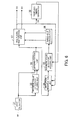
- FIG. 4 is a block diagram of a configuration of a demodulation circuit according to the second embodiment. As shown in this figure, the demodulation circuit comprises a
wave detector 21, a maximum value detector/holdingunit 22, anamplitude binarization unit 23, a minimum value detector/holdingunit 24, athreshold calculator 25, amultilevel restoration unit 26, and asampling timing generator 27. - The
wave detector 21 obtains a multilevel signal from a radio signal RF received by an antenna, as in thewave detector 11 described with FIG. 1. The multilevel signal is output to the maximum value detector/holdingunit 22, theamplitude binarization unit 23, and themultilevel restoration unit 26. - The maximum value detector/holding
unit 22 detects and holds the maximum value of the electric current of the multilevel signal received from thewave detector 21. The maximum value detector/holdingunit 22 outputs the held maximum value of the electric current of the multilevel signal to thethreshold calculator 25. - The
amplitude binarization unit 23 causes the amplitude of the multilevel signal received from thewave detector 21 to have the maximum value and the minimum value alternately. For example, even if a multilevel signal (here, a three-level signal) of intermediate level is output, a level corresponding to the maximum value and a level corresponding to the minimum value are alternately output. In addition, even if the multilevel signal continues its maximum value, the maximum value level and the minimum value level are always output alternately. - The
amplitude binarization unit 23 receives received data D0 and D1 from themultilevel restoration unit 26, and depending on the H state and L state of the received data D0 and D1, recognizes that the multilevel signal output from thewave detector 21 is intermediate level, and also recognizes that the multilevel signal output from thewave detector 21 continues its maximum value. - The minimum value detector/holding
unit 24 detects and holds the minimum value of the electric current of the multilevel signal received from theamplitude binarization unit 23. The minimum value detector/holdingunit 24 outputs the held minimum value of the multilevel signal to thethreshold calculator 25. The minimum value detector/holdingunit 24 holds the minimum value of the electric current of the binarized multilevel signal received from theamplitude binarization unit 23, in accordance with a timing signal coming from thesampling timing generator 27 that will be described later. - The
threshold calculator 25 calculates thresholds to be used for reconstructing received data D0 and D1 from the multilevel signal, from the maximum value of the amplitude of the multilevel signal received from the maximum value detector/holdingunit 22 and the minimum value of the amplitude of the multilevel signal received from the minimum value detector/holdingunit 24, as in thethreshold calculator 13 described with FIG. 1. - The
multilevel restoration unit 26 compares the multilevel signal received from thewave detector 11 with each threshold received from thethreshold calculator 13, as in themultilevel restoration unit 14 described with FIG. 1. Then themultilevel restoration unit 26 obtains information indicating H state and L state, included in the multilevel signal, depending on whether the electric current of the multilevel signal is greater than the thresholds, and reconstructs the received data D0 and D1 included in the multilevel signal. - The
sampling timing generator 27 receives the received data D0 from themultilevel restoration unit 26. Thesampling timing generator 27 generates a timing signal of a fixed period based on the received data D0. - Now, reconstruction of received data from a multilevel signal will be described with reference to views of signal waveforms.
- FIG. 5 is views for explaining how to reconstruct received data from a multilevel signal. A waveform W11 of the figure (A) is a waveform of a three-level signal output from the
wave detector 21. In the case of three-level signal, there is an intermediate level in addition to levels corresponding to H state and L state, as shown in this figure. In addition, a waveform W12 of the figure (A) shows the maximum value of the amplitude of the multilevel signal. That is, the maximum value detector/holdingunit 22 holds the electric current value shown by the waveform W12, and outputs the same to thethreshold calculator 25. The figure (B) shows a waveform obtained by binarizing the waveform W11 of the figure (A) into an amplitude of the maximum value and the minimum value. That is, the figure (B) shows the electric current value that is output from theamplitude binarization unit 23. The figure (C) shows the minimum current value of the multilevel signal held by the minimum value detector/holdingunit 24. The figure (D) shows received data D0 output from themultilevel restoration unit 26. The figure (E) shows received data D1 output from themultilevel restoration unit 26. The figure (F) shows a timing signal output from thesampling timing generator 27. - From the
wave detector 21 of FIG. 4, a multilevel signal shown by the waveform W11 of the figure (A) is output. The maximum value detector/holdingunit 22 holds the maximum value of the multilevel signal received from thewave detector 21, which is shown by the waveform W12 of the figure (A), and outputs the same to thethreshold calculator 25. - The
amplitude binarization unit 23 binarizes the multilevel signal that outputs intermediate level and H state continuously, as shown in the figure (B), and outputs the resultant to the minimum value detector/holdingunit 24. In the case where the received data D0 is L state and the received data D1 is H state, as shown by arrows of this figure, theamplitude binarization unit 23 recognizes that the multilevel signal is intermediate level, and in this case, it causes the multilevel signal to have the minimum value. In addition, in the case where the received data D0 and D1 continue their H states, as shown by arrows of this figure, theamplitude binarization unit 23 recognizes that the multilevel signal continues its H state, and in this case, it causes the multilevel signal to have the minimum value so as not to continue the H state. In order to obtain the minimum value of the amplitude from the intermediate level, a difference between the maximum value and the intermediate level is calculated, and a doubled value of the difference is subtracted from the maximum value, thereby calculating the minimum value, for example. In addition, in order to obtain the minimum value of the amplitude from the maximum value, the maximum value is multiplied by a predetermined value (one or smaller), thereby calculating the minimum value, for example. - The minimum value detector/holding
unit 24 holds the minimum value of the binarized multilevel signal, which is shown in the figure (C), and outputs the same to thethreshold calculator 25, in accordance with a timing signal coming from thesampling timing generator 27 shown in the figure (F). - The
threshold calculator 25 calculates thresholds IthA and IthB shown in the figure (A), from the maximum value of the amplitude of the multilevel signal received from the maximum value detector/holdingunit 22 and the minimum value of the amplitude of the multilevel signal received from the minimum value detector/holdingunit 24. - The
multilevel restoration unit 26 compares the threshold IthA received from thethreshold calculator 25 with the multilevel signal, and outputs the received data D1 shown in the figure (D). In addition, themultilevel restoration unit 26 compares the threshold IthB received from thethreshold calculator 25 with the multilevel signal, and outputs the received data D0 shown in the figure (E). - The
sampling timing generator 27 has a counter, and when a prescribed number is counted after the received data D0 falls, outputs a timing signal of pulse width much smaller than the pulse width of the received data D0, which is shown in the figure (F). If the received data D0 continues its H state, thesampling timing generator 27 periodically outputs a timing signal with reference to a last count value. - As described above, in the case where a multilevel signal continues its intermediate level and H state, the multilevel signal is binarized to accurately obtain the minimum value of the multilevel signal, so that the received data D0 and D1 can be reconstructed. Therefore, many data can be completely received without increasing a transfer speed.
- Now, the third embodiment of this invention will be described in detail with reference to accompanying drawings. In the third embodiment, the electric current of a multilevel signal output from a wave detector is made to have a minimum value of zero, thereby simplifying signal processing of a circuit.
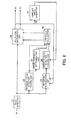
- FIG. 6 is a block diagram of a configuration of a demodulation circuit according to the third embodiment. As shown in this figure, the demodulation circuit comprises a
wave detector 31, a maximum value detector/holdingunit 32, adifferentiation unit 33, anamplitude binarization unit 34, a maximum value detector/holdingunit 35, athreshold calculator 36, amultilevel restoration unit 37, and asampling timing generator 38. - The
wave detector 31 obtains a multilevel signal from a radio signal RF received by an antenna, as in thewave detector 11 described with FIG. 1. The multilevel signal is output to the maximum value detector/holdingunit 32 and thedifferentiation unit 33. - The maximum value detector/holding
unit 32 detects and holds the maximum value of the electric current of the multilevel signal received from thewave detector 31. The maximum value detector/holdingunit 32 outputs the held maximum value of the electric current of the multilevel signal to thedifferentiation unit 33. - The
differentiation unit 33 subtracts the multilevel signal received from thewave detector 31 from the maximum value of the electric current of the multilevel signal held by the maximum value detector/holdingunit 32, and outputs the resultant. Thereby the multilevel signal to be output from thedifferentiation unit 33 is a reversed signal of the multilevel signal and has a minimum current value of zero. By causing the multilevel signal to have zero as the electric current of the minimum level, signal processing to be performed by a circuit of latter stage is simplified. The reversed multilevel signal from thedifferentiation unit 33 is output to theamplitude binarization unit 34 and themultilevel restoration unit 37. - The
amplitude binarization unit 34 binarizes the reversed multilevel signal received from thedifferentiation unit 33, based on the received data D0 and D1 received from themultilevel restoration unit 37, as in theamplitude binarization unit 23 of FIG. 4. That is, even if the multilevel signal (a three-level signal is used for this explanation) of intermediate level is output, theamplitude binarization unit 34 always outputs a level corresponding to H state and a level corresponding to L state alternately. In addition, even if the multilevel signal continues its minimum value, theamplitude binarization unit 34 always outputs the maximum value level and the minimum value level alternately. - The maximum value detector/holding
unit 35 detects and holds the maximum value of the multilevel signal received from theamplitude binarization unit 34. The multilevel signal has been reversed by thedifferentiation unit 33 and its electric current of minimum level is zero, as described above, so that the maximum value is to be held here. The maximum value detector/holdingunit 35 holds the maximum value of the electric current of the binarized multilevel signal received from theamplitude binarization unit 34, in accordance with a timing signal coming from thesampling timing generator 38 that will be described later. - The
threshold calculator 36 calculates thresholds to be used for reconstructing received data D0 and D1 from a multilevel signal, from the maximum value of the amplitude of the multilevel signal received from the maximum value detector/holdingunit 35, as in thethreshold calculator 13 described with FIG. 1. It should be noted that the amplitude of the multilevel signal has been made to have a minimum value of zero by thedifferentiation unit 33. - The
multilevel restoration unit 37 compares the multilevel signal reversed by thedifferentiation unit 33 with each threshold received from thethreshold calculator 36. Then themultilevel restoration unit 37 obtains information indicating H state and L state, included in the multilevel signal, depending on whether the electric current of the multilevel signal output from thedifferentiation unit 33 is greater than the thresholds, and reconstructs the received data D0 and D1 included in the multilevel signal. - The
sampling timing generator 38 generates a timing signal of a fixed period based on the received data D0, as in thesampling timing generator 27 described with FIG. 4. The timing signal is output to the maximum value detector/holdingunit 35. - Now, reconstruction of received data from a multilevel signal will be described with reference to views of signal waveforms.
- FIG. 7 is views for explaining how to reconstruct received data from a multilevel signal. A waveform W21 of the figure (A) is a waveform of a three-level signal output from the
wave detector 21. In the case of three-level signal, there is an intermediate level in addition to levels corresponding to H state and L state, as shown in this figure. In addition, a waveform W22 of the figure (A) shows the maximum value of the amplitude of the multilevel signal. That is, the maximum value detector/holdingunit 32 holds the electric current value shown by the waveform W22 and outputs the same to thedifferentiation unit 33. The figure (B) shows electric current output from thedifferentiation unit 33. Thedifferentiation unit 33 outputs the electric current obtained by subtracting the multilevel signal from the maximum value output from the maximum value detector/holdingunit 32, in which the electric current has a minimum value of zero and is a reversed signal of the multilevel signal, as shown in this figure. The figure (C) shows a binarized multilevel signal output from theamplitude binarization unit 34. The figure (D) shows zero that is the minimum current value of the binarized multilevel signal and the maximum current Imax held by the maximum value detector/holdingunit 35. The figure (E) shows received data D0 output from themultilevel restoration unit 37. The figure (F) shows received data D1 output from themultilevel restoration unit 37. The figure (G) shows a timing signal output from thesampling timing generator 38. - From the
wave detector 31 of FIG. 6, the multilevel signal shown by the waveform W21 of the figure (A) is output. The maximum value detector/holdingunit 32 holds the maximum value of the multilelvel signal received from thewave detector 31, which is shown by the waveform W22 of the figure (A), and outputs it to thedifferentiation unit 33. - The
differentiation unit 33 subtracts the multilevel signal from the maximum value held by the maximum value detector/holdingunit 32, and outputs a multilevel signal which has a minimum value of zero and has a reversed waveform, which is shown in the figure (B). - The
amplitude binarization unit 34 binarizes the multilevel signal received from thedifferentiation unit 33, and outputs the resultant to the maximum value detector/holdingunit 35, which is shown in the figure (C). In order to obtain the maximum value of the amplitude from intermediate level, a doubled value of the intermediate level is taken as the maximum value, for example. In addition, in order to obtain the maximum value of the amplitude from the minimum value, a predetermined value is added to the minimum value and its result is taken as the maximum value, for example. By setting the minimum level to zero in this way, the binarization process is simplified. - The maximum value detector/holding
unit 35 holds the maximum value (electric current Imax) of the binarized multilevel signal, which is shown in the figure (D), and outputs it to thethreshold calculator 36, in accordance with the timing signal coming from thesampling timing generator 38 shown in the figure (G). - The
threshold calculator 36 calculates thresholds IthA and IthB, which are shown in the figure (A), from the maximum value of the amplitude of the multilevel signal received from the maximum value detector/holdingunit 35. It should be noted that, since it is known that the minimum value of the amplitude is zero, the thresholds IthA and IthB can be easily calculated only from the maximum value of the amplitude. - The
multilelvel restoration unit 37 compares the threshold IthA received from thethreshold calculator 36 with the multilevel signal, and outputs the received data D0 shown in the figure (E). In addition, themultilevel restoration unit 37 compares the threshold IthB received from thethreshold calculator 36 with the multilevel signal, and outputs the received data D1 shown in the figure (F). - As described above, the minimum value of the multilevel signal, that is, a standard level is set to 0, so that the signal processing to be performed by a circuit of latter stage can be simplified. In addition, the setting of the standard level to zero decreases power consumption.
- Now the fourth embodiment of this invention will be described in detail with reference to accompanying drawings. In the fourth embodiment, an initial threshold to be used for reconstructing received data from a multilevel signal is determined, and for example, a threshold calculator reconstructs received data by using the initial threshold when the demodulation circuit starts to operate.
- FIG. 8 is a block diagram of a configuration of a demodulation circuit according to the fourth embodiment. The same reference numerals as FIG. 4 are given to the same components of FIG. 8 and explanation of them will be omitted.
- A multilevel signal output from a
wave detector 21 continues its peak current before signal transmission starts, as described with FIG. 2. Then the signal becomes a signal including information. An initialthreshold determination unit 41 calculates an initial threshold based on the first peak current, and outputs it to thethreshold calculator 42. - The initial
threshold determination unit 41 sets predetermined times peak current as a threshold. Consider a case of a binary signal. If it is determined that a value equal to or lower than an electric current value obtained by multiplying the peak current by 0.7 indicates L state, a threshold can be determined by multiplying the peak current by 0.85. That is, a value greater than an electric current value obtained by multiplying the peak current by 0.85 indicates H state, while a value equal to or lower than the electric current value indicates L state. Similarly, for a three-level signal, an initial threshold can be determined from the peak current. - The
threshold calculator 42 outputs the threshold calculated by the initialthreshold determination unit 41 to themultilevel restoration unit 26 when the signal transmission starts. Then the signal transmission starts and when a multilevel signal including information indicating H state and L state is output, thethreshold calculator 42 calculates thresholds to be used for reconstructing received data D0 and D1 from the multilevel signal, from the maximum value and the minimum value of the amplitude of the multilevel signal received from the maximum value detector/holdingunit 22 and the minimum value detector/holdingunit 24, in the same way described with FIG. 4. - By calculating an initial threshold from the peak current when the signal transmission starts as described above, it becomes possible to distinguish, from a signal, noise that is superimposed on the peak current when the signal transmission starts.
- Now the fifth embodiment of this invention will be described in detail with reference to accompanying drawings. In the restoration circuit of FIG. 4, the minimum value detector/holding
unit 24 detects and holds the minimum value of the binarized multilevel signal. Noise superimposed on the multilevel signal may have an influence on the minimum value to be held. For this case, this fifth embodiment enables decrease of an influence of noise on the minimum value. In the fifth embodiment, another function is added to the minimum value detector/holdingunit 24 of FIG. 4 and the other components are identical. Therefore, a block diagram of a configuration is not provided and its description is made with reference to FIG. 4. - A minimum value detector/holding
unit 24 is designed to output 50% of a change in minimum value of the multilevel signal, the minimum value varying due to noise. That is, the minimum value detector/holdingunit 24 multiplies the change in the minimum value of the multilevel signal caused by the noise (change between a previous minimum value and a current minimum value) by a coefficient (a value of one or lower), to thereby suppress the influence of the noise. - Now, reconstruction of received data from a multilevel signal will be described with reference to views of signal waveforms.
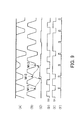
- FIG. 9 is views for explaining how to reconstruct received data from a multilevel signal. The figure (A) shows a waveform of a three-level signal output from the
wave detector 21 of FIG. 4. In the case of three-level signal, there is an intermediate level in addition to levels corresponding to H state and L state. In addition, noise is superimposed on a multilevel signal, and therefore its minimum value varies as shown in this figure. the figure (B) shows a waveform obtained by binarizing the multilevel signal of the figure (A) into an amplitude of a maximum value and a minimum value. That is, this figure shows the electric current value that is output from anamplitude binarization unit 23. Since the minimum value of the multilevel signal varies due to noise as described above, the minimum value of the binarized multilevel signal varies as well. - The figure (C) shows the minimum value held and output by the minimum value detector/holding
unit 24. The minimum value detector/holdingunit 24 of the fifth embodiment outputs 50% of a change in minimum value of the binarized multilevel signal. For example, 50% of a change between the minimum values M11 and M12 shown in the figure (B) is output as shown in the figure (C). In addition, 50% of a change between the minimum values M12 and M13 is output as shown in the figure (C). - The figure (D) shows received data D0 output from a
multilevel restoration unit 26. The figure (E) shows received data D1 output from themultilevel restoration unit 26. The figure (F) shows a timing signal output from asampling timing generator 27. - As described above, by suppressing an influence of noise superimposed on the minimum value of a binarized multilevel signal, appropriate thresholds can be calculated.
- It should be noted that the above noise suppression can be applied to the third embodiment. That is, similarly to the above minimum value detector/holding
unit 24, the maximum value detector/holdingunit 35 of FIG. 6 may multiply a change in maximum value of a multilevel signal which is caused due to noise, by a coefficient, thereby suppressing an influence of the noise. - The foregoing is considered as illustrative only of the principle of the present invention. Further, since numerous modifications and changes will readily occur to those skilled in the art, it is not desired to limit the invention to the exact construction and applications shown and described, and accordingly, all suitable modifications and equivalents may be regarded as falling within the scope of the invention in the appended claims and their equivalents.
-
- 11
- wave detector
- 12
- amplitude detector
- 13
- threshold calculator
- 14
- multilevel restoration unit
- RF
- radio signal
- D0 to Dn
- received data
Claims (10)
- A demodulation circuit restoring a multilevel signal received on radio, comprising:an amplitude detector detecting a maximum value and a minimum value of an amplitude of the multilevel signal;a threshold calculator calculating a plurality of thresholds to be used for determining whether the multilevel signal is H sate or L state, from the maximum value and the minimum value; anda multilevel restoration unit comparing the multilevel signal with each of the thresholds to detect the H state and the L state, and reconstructing a plurality of received data.
- The demodulation circuit according to claim 1, wherein the threshold calculator calculates the thresholds so that the amplitude of the multilevel signal is divided into N (N is a positive integral number of three or greater).
- The demodulation circuit according to claim 1, wherein the amplitude detector comprises:a maximum value detector detecting the maximum value of the multilevel signal;an amplitude binarization unit binarizing the amplitude of the multilevel signal into the maximum value and the minimum value; anda minimum value detector detecting the minimum value from the multilevel signal binarized.
- The demodulation circuit according to claim 3, wherein the minimum value detector outputs a value obtained by multiplying by a prescribed coefficient a difference between the minimum value detected last and the minimum value detected this time.
- The demodulation circuit according to claim 1, further comprising an initial threshold determination unit calculating an initial threshold from peak current of the multilevel signal detected before signal transmission starts.
- A demodulation circuit restoring a multilevel signal received on radio, comprising:a first maximum value detector detecting a maximum value of the multilevel signal;a multilevel signal subtraction unit subtracting the multilevel signal from the maximum value and outputting a reversed signal;an amplitude binarization unit binarizing an amplitude of the reversed signal into a maximum value and a minimum value;a second maximum value detector detecting the maximum value of the reversed signal binarized;a threshold calculator calculating a plurality of thresholds to be used for determining the reversed signal is H state or L state, from the maximum value detected by the second maximum value detector; anda multilevel restoration unit comparing the reversed signal with each of the thresholds to detect the H state and the L state, and reconstructing a plurality of received data.
- The demodulation circuit according to claim 6, wherein the threshold calculator calculates the thresholds so that the amplitude of the reversed signal is divided into N (N is a positive integral number of 3 or greater).
- The demodulation circuit according to claim 6, wherein the second maximum value detector outputs a value obtained by multiplying by a prescribed coefficient a difference between the maximum value detected last and the maximum value detected this time.
- An electronic device receiving on radio and restoring a multilevel signal, comprising:an amplitude detector detecting a maximum value and a minimum value of an amplitude of the multilevel signal;a threshold calculator calculating a plurality of thresholds to be used for determining whether the multilevel signal is H sate or L state, from the maximum value and the minimum value; anda multilevel restoration unit comparing the multilevel signal with each of the thresholds to detect the H state and the L state, and reconstructing a plurality of received data.
- An electronic device receiving on radio and restoring a multilevel signal, comprising:a first maximum value detector detecting a maximum value of the multilevel signal;a multilevel signal subtraction unit subtracting the multilevel signal from the maximum value and outputting a reversed signal;an amplitude binarization unit binarizing an amplitude of the reversed signal into a maximum value and a minimum value;a second maximum value detector detecting the maximum value of the reversed signal binarized;a threshold calculator calculating a plurality of thresholds to be used for determining the reversed signal is H state or L state, from the maximum value detected by the second maximum value detector; anda multilevel restoration unit comparing the reversed signal with each of the thresholds to detect the H state and the L state, and reconstructing a plurality of received data.
Applications Claiming Priority (1)
| Application Number | Priority Date | Filing Date | Title |
|---|---|---|---|
| PCT/JP2005/003342 WO2006092843A1 (en) | 2005-02-28 | 2005-02-28 | Modulation circuit and electronic device |
Publications (3)
| Publication Number | Publication Date |
|---|---|
| EP1855432A1 true EP1855432A1 (en) | 2007-11-14 |
| EP1855432A4 EP1855432A4 (en) | 2011-04-13 |
| EP1855432B1 EP1855432B1 (en) | 2012-08-08 |
Family
ID=36940889
Family Applications (1)
| Application Number | Title | Priority Date | Filing Date |
|---|---|---|---|
| EP05719659A Expired - Lifetime EP1855432B1 (en) | 2005-02-28 | 2005-02-28 | Modulation circuit and electronic device |
Country Status (5)
| Country | Link |
|---|---|
| US (1) | US7545879B2 (en) |
| EP (1) | EP1855432B1 (en) |
| JP (1) | JP4573871B2 (en) |
| KR (1) | KR100936200B1 (en) |
| WO (1) | WO2006092843A1 (en) |
Families Citing this family (6)
| Publication number | Priority date | Publication date | Assignee | Title |
|---|---|---|---|---|
| JP2008123084A (en) * | 2006-11-09 | 2008-05-29 | Yokogawa Electric Corp | Transmission line abnormality diagnosis field device system |
| JP4766002B2 (en) * | 2007-05-29 | 2011-09-07 | 株式会社デンソー | ASK receiver circuit |
| JP5107777B2 (en) * | 2008-04-10 | 2012-12-26 | 株式会社日立製作所 | Receiving device, reader / writer, and RFID system |
| EP2688232B1 (en) * | 2012-07-19 | 2017-06-14 | Alcatel Lucent | Optical transmitter for transmitting a multilevel amplitude-shift-keying modulated signal |
| KR102110841B1 (en) | 2013-08-01 | 2020-05-14 | 삼성전자주식회사 | Method and apparatus of setting threshold adaptively for demodulating signal |
| JP7004503B2 (en) * | 2017-01-27 | 2022-01-21 | ラピスセミコンダクタ株式会社 | Automatic gain control circuit (AGC), despreading circuit and method of reproducing received data |
Family Cites Families (13)
| Publication number | Priority date | Publication date | Assignee | Title |
|---|---|---|---|---|
| JPH03283742A (en) * | 1990-03-30 | 1991-12-13 | Omron Corp | Method and apparatus for shaping waveform and method and apparatus for generating threshold value for waveform shaping |
| EP0678999B1 (en) | 1994-04-08 | 2001-09-26 | Nec Corporation | Adaptive setting of decision thresholds |
| KR0139657B1 (en) * | 1994-11-09 | 1998-07-01 | 문정환 | Signal receiver with automatic level selection |
| JPH09205466A (en) * | 1996-01-29 | 1997-08-05 | Kokusai Electric Co Ltd | Symbol determination device |
| US5832038A (en) * | 1996-07-03 | 1998-11-03 | Motorola, Inc. | Method and apparatus for classifying a multi-level signal |
| JPH10145442A (en) * | 1996-11-07 | 1998-05-29 | Nec Shizuoka Ltd | Wireless selective call receiving system and wireless selective call receiving method |
| JPH10163877A (en) * | 1996-11-28 | 1998-06-19 | Sony Corp | Threshold control circuit of multi-level comparator in demodulation circuit |
| JP3526719B2 (en) | 1997-03-19 | 2004-05-17 | 富士通株式会社 | Automatic threshold control circuit and signal amplifier circuit |
| TW445718B (en) | 1999-03-26 | 2001-07-11 | Matsushita Electric Industrial Co Ltd | Discriminator |
| JP2000349605A (en) * | 1999-03-26 | 2000-12-15 | Matsushita Electric Ind Co Ltd | Identification circuit |
| FR2806855B1 (en) | 2000-03-21 | 2002-06-21 | St Microelectronics Sa | AMPLITUDE MODULATED ALTERNATIVE SIGNAL DEMODULATOR |
| JP3683550B2 (en) * | 2002-04-22 | 2005-08-17 | シャープ株式会社 | Binarization circuit, radio communication apparatus and binarization method |
| JP4265487B2 (en) | 2004-06-17 | 2009-05-20 | 富士通株式会社 | Reader device, method of transmitting the device, and tag |
-
2005
- 2005-02-28 JP JP2007505763A patent/JP4573871B2/en not_active Expired - Fee Related
- 2005-02-28 KR KR1020077019568A patent/KR100936200B1/en not_active Expired - Fee Related
- 2005-02-28 EP EP05719659A patent/EP1855432B1/en not_active Expired - Lifetime
- 2005-02-28 WO PCT/JP2005/003342 patent/WO2006092843A1/en not_active Ceased
-
2007
- 2007-08-27 US US11/892,699 patent/US7545879B2/en not_active Expired - Fee Related
Also Published As
| Publication number | Publication date |
|---|---|
| JPWO2006092843A1 (en) | 2008-08-07 |
| WO2006092843A1 (en) | 2006-09-08 |
| KR100936200B1 (en) | 2010-01-11 |
| JP4573871B2 (en) | 2010-11-04 |
| US7545879B2 (en) | 2009-06-09 |
| KR20070101358A (en) | 2007-10-16 |
| US20070291879A1 (en) | 2007-12-20 |
| EP1855432A4 (en) | 2011-04-13 |
| EP1855432B1 (en) | 2012-08-08 |
Similar Documents
| Publication | Publication Date | Title |
|---|---|---|
| US7545879B2 (en) | Demodulation circuit and electronic device | |
| US7405659B1 (en) | RFID tag switched capacitor slicer threshold | |
| US8923705B2 (en) | Poisson-based communication system and methods | |
| US8188787B2 (en) | Peak detector for detecting peaks in a modulated signal | |
| US8325786B2 (en) | Semiconductor device and communication device | |
| US9893771B2 (en) | Wireless charger using frequency aliasing FSK demodulation | |
| EP0993652A1 (en) | Data carrier having rectifier means and having improved voltage limiting means | |
| KR100411562B1 (en) | Method for ask demodulation and ask demodulator | |
| JPH04502245A (en) | Code acquisition method and circuit for a receiver of spread spectrum signals | |
| US6886752B2 (en) | Portable electronic apparatus, IC card and reader/writer | |
| CA2397107C (en) | Encoding/decoding system for coherent signal interference reduction | |
| US8111781B2 (en) | Radio frequency identification (RFID) interrogators | |
| US7614564B2 (en) | Clock generation method and device for decoding from an asynchronous data signal | |
| US20180159706A1 (en) | Radio-Frequency Apparatus with Digital Signal Arrival Detection and Associated Methods | |
| CN114266264B (en) | Signal demodulation method, device, receiver and computer-readable storage medium | |
| RU2460224C1 (en) | Differential phase-shift keyed signal demodulator | |
| JPH11251960A (en) | Path detection method and apparatus for direct spread spectrum communication system | |
| US7439800B2 (en) | Amplitude demodulator for an electromagnetic transponder | |
| EP3667935B1 (en) | Method and system for operating a communications device that communicates via inductive coupling | |
| US20240340156A1 (en) | System and method for timing recovery in high bandwidth communications | |
| CN104639483A (en) | Digital correlation demodulation circuit based on 14443-BPSK (binary phase shift keying) subcarriers | |
| US20240195665A1 (en) | Asynchronous bit detection mechanism for ask demodulators | |
| US20110013674A1 (en) | Timing regenerating device | |
| JP3881590B2 (en) | Phase detection circuit and phase detection method | |
| RU2017337C1 (en) | Delay-pulse pseudorandom noise discriminator |
Legal Events
| Date | Code | Title | Description |
|---|---|---|---|
| PUAI | Public reference made under article 153(3) epc to a published international application that has entered the european phase |
Free format text: ORIGINAL CODE: 0009012 |
|
| 17P | Request for examination filed |
Effective date: 20070822 |
|
| AK | Designated contracting states |
Kind code of ref document: A1 Designated state(s): DE FR GB |
|
| DAX | Request for extension of the european patent (deleted) | ||
| RBV | Designated contracting states (corrected) |
Designated state(s): DE FR GB |
|
| A4 | Supplementary search report drawn up and despatched |
Effective date: 20110310 |
|
| RIC1 | Information provided on ipc code assigned before grant |
Ipc: H04L 7/00 20060101ALI20110304BHEP Ipc: H03K 5/08 20060101ALI20110304BHEP Ipc: H04L 25/06 20060101ALI20110304BHEP Ipc: H04L 25/08 20060101ALI20110304BHEP Ipc: H04L 25/49 20060101ALI20110304BHEP Ipc: H04L 27/06 20060101AFI20060912BHEP Ipc: H03K 9/02 20060101ALI20110304BHEP |
|
| 17Q | First examination report despatched |
Effective date: 20110520 |
|
| GRAP | Despatch of communication of intention to grant a patent |
Free format text: ORIGINAL CODE: EPIDOSNIGR1 |
|
| RIC1 | Information provided on ipc code assigned before grant |
Ipc: H03K 5/08 20060101ALI20120215BHEP Ipc: H03K 9/02 20060101ALI20120215BHEP Ipc: H04L 27/06 20060101AFI20120215BHEP Ipc: H04L 27/08 20060101ALI20120215BHEP Ipc: H04L 25/06 20060101ALI20120215BHEP Ipc: H04L 25/49 20060101ALI20120215BHEP Ipc: H04L 7/00 20060101ALI20120215BHEP |
|
| RTI1 | Title (correction) |
Free format text: MODULATION CIRCUIT AND ELECTRONIC DEVICE |
|
| GRAS | Grant fee paid |
Free format text: ORIGINAL CODE: EPIDOSNIGR3 |
|
| GRAA | (expected) grant |
Free format text: ORIGINAL CODE: 0009210 |
|
| AK | Designated contracting states |
Kind code of ref document: B1 Designated state(s): DE FR GB |
|
| REG | Reference to a national code |
Ref country code: GB Ref legal event code: FG4D |
|
| REG | Reference to a national code |
Ref country code: DE Ref legal event code: R096 Ref document number: 602005035514 Country of ref document: DE Effective date: 20121011 |
|
| PLBE | No opposition filed within time limit |
Free format text: ORIGINAL CODE: 0009261 |
|
| STAA | Information on the status of an ep patent application or granted ep patent |
Free format text: STATUS: NO OPPOSITION FILED WITHIN TIME LIMIT |
|
| 26N | No opposition filed |
Effective date: 20130510 |
|
| REG | Reference to a national code |
Ref country code: DE Ref legal event code: R097 Ref document number: 602005035514 Country of ref document: DE Effective date: 20130510 |
|
| REG | Reference to a national code |
Ref country code: FR Ref legal event code: PLFP Year of fee payment: 12 |
|
| PGFP | Annual fee paid to national office [announced via postgrant information from national office to epo] |
Ref country code: DE Payment date: 20160223 Year of fee payment: 12 |
|
| PGFP | Annual fee paid to national office [announced via postgrant information from national office to epo] |
Ref country code: FR Payment date: 20160108 Year of fee payment: 12 Ref country code: GB Payment date: 20160224 Year of fee payment: 12 |
|
| REG | Reference to a national code |
Ref country code: DE Ref legal event code: R119 Ref document number: 602005035514 Country of ref document: DE |
|
| GBPC | Gb: european patent ceased through non-payment of renewal fee |
Effective date: 20170228 |
|
| REG | Reference to a national code |
Ref country code: FR Ref legal event code: ST Effective date: 20171031 |
|
| PG25 | Lapsed in a contracting state [announced via postgrant information from national office to epo] |
Ref country code: DE Free format text: LAPSE BECAUSE OF NON-PAYMENT OF DUE FEES Effective date: 20170901 Ref country code: FR Free format text: LAPSE BECAUSE OF NON-PAYMENT OF DUE FEES Effective date: 20170228 |
|
| PG25 | Lapsed in a contracting state [announced via postgrant information from national office to epo] |
Ref country code: GB Free format text: LAPSE BECAUSE OF NON-PAYMENT OF DUE FEES Effective date: 20170228 |