EP1854637A1 - Printer and ic chip communication device - Google Patents
Printer and ic chip communication device Download PDFInfo
- Publication number
- EP1854637A1 EP1854637A1 EP06715074A EP06715074A EP1854637A1 EP 1854637 A1 EP1854637 A1 EP 1854637A1 EP 06715074 A EP06715074 A EP 06715074A EP 06715074 A EP06715074 A EP 06715074A EP 1854637 A1 EP1854637 A1 EP 1854637A1
- Authority
- EP
- European Patent Office
- Prior art keywords
- antenna
- transporting path
- printer according
- sheet
- distance
- Prior art date
- Legal status (The legal status is an assumption and is not a legal conclusion. Google has not performed a legal analysis and makes no representation as to the accuracy of the status listed.)
- Granted
Links
Images




Classifications
-
- B—PERFORMING OPERATIONS; TRANSPORTING
- B41—PRINTING; LINING MACHINES; TYPEWRITERS; STAMPS
- B41J—TYPEWRITERS; SELECTIVE PRINTING MECHANISMS, i.e. MECHANISMS PRINTING OTHERWISE THAN FROM A FORME; CORRECTION OF TYPOGRAPHICAL ERRORS
- B41J3/00—Typewriters or selective printing or marking mechanisms characterised by the purpose for which they are constructed
- B41J3/407—Typewriters or selective printing or marking mechanisms characterised by the purpose for which they are constructed for marking on special material
- B41J3/4075—Tape printers; Label printers
-
- B—PERFORMING OPERATIONS; TRANSPORTING
- B41—PRINTING; LINING MACHINES; TYPEWRITERS; STAMPS
- B41J—TYPEWRITERS; SELECTIVE PRINTING MECHANISMS, i.e. MECHANISMS PRINTING OTHERWISE THAN FROM A FORME; CORRECTION OF TYPOGRAPHICAL ERRORS
- B41J3/00—Typewriters or selective printing or marking mechanisms characterised by the purpose for which they are constructed
- B41J3/44—Typewriters or selective printing mechanisms having dual functions or combined with, or coupled to, apparatus performing other functions
-
- G—PHYSICS
- G06—COMPUTING OR CALCULATING; COUNTING
- G06K—GRAPHICAL DATA READING; PRESENTATION OF DATA; RECORD CARRIERS; HANDLING RECORD CARRIERS
- G06K17/00—Methods or arrangements for effecting co-operative working between equipments covered by two or more of main groups G06K1/00 - G06K15/00, e.g. automatic card files incorporating conveying and reading operations
- G06K17/0022—Methods or arrangements for effecting co-operative working between equipments covered by two or more of main groups G06K1/00 - G06K15/00, e.g. automatic card files incorporating conveying and reading operations arrangements or provisions for transferring data to distant stations, e.g. from a sensing device
- G06K17/0025—Methods or arrangements for effecting co-operative working between equipments covered by two or more of main groups G06K1/00 - G06K15/00, e.g. automatic card files incorporating conveying and reading operations arrangements or provisions for transferring data to distant stations, e.g. from a sensing device the arrangement consisting of a wireless interrogation device in combination with a device for optically marking the record carrier
-
- H—ELECTRICITY
- H01—ELECTRIC ELEMENTS
- H01Q—ANTENNAS, i.e. RADIO AERIALS
- H01Q1/00—Details of, or arrangements associated with, antennas
- H01Q1/12—Supports; Mounting means
- H01Q1/125—Means for positioning
-
- H—ELECTRICITY
- H01—ELECTRIC ELEMENTS
- H01Q—ANTENNAS, i.e. RADIO AERIALS
- H01Q1/00—Details of, or arrangements associated with, antennas
- H01Q1/12—Supports; Mounting means
- H01Q1/22—Supports; Mounting means by structural association with other equipment or articles
- H01Q1/2208—Supports; Mounting means by structural association with other equipment or articles associated with components used in interrogation type services, i.e. in systems for information exchange between an interrogator/reader and a tag/transponder, e.g. in Radio Frequency Identification [RFID] systems
- H01Q1/2216—Supports; Mounting means by structural association with other equipment or articles associated with components used in interrogation type services, i.e. in systems for information exchange between an interrogator/reader and a tag/transponder, e.g. in Radio Frequency Identification [RFID] systems used in interrogator/reader equipment
Definitions
- the present invention relates to a printer and an IC tag reading/writing apparatus that performs printing on a sheet or writes information to an IC tag serving as an IC chip and provided on this sheet.
- the IC tag provided on the label sheet which is the subject in the label printer, is generally an RF (Radio Frequency) tag, wherein information is wirelessly written and read.
- RF Radio Frequency
- Patent Reference 1 Japanese Unexamined Patent Publication No. 2001-331768
- an object of the present invention is to provide a label printer, which performs printing to a label sheet provided with an IC tag and writes data to the IC tag, and which can cope with various types of label sheets.
- a label printer includes a print head that performs printing to a sheet provided with an IC chip; a transporting device that transports the sheet on a transporting path; an antenna that mediates data communication with the IC chip provided on the sheet transported on the transporting path; and a mechanism for adjusting a distance between the antenna and the transporting path.
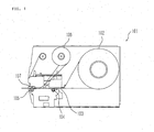
- FIG. 1 is a longitudinal side view schematically showing a structure of a label printer 101.
- a transport roller 104 that serves as a transporting device for drawing a label sheet, which is wound in a roll fashion, from the rolled state so as to transport the label sheet 102 on a sheet transporting path 103
- a platen roller 105 that serves as a transporting device for drawing a label sheet, which is wound in a roll fashion, from the rolled state so as to transport the label sheet 102 on a sheet transporting path 103
- a platen roller 105 an ink ribbon 106
- a thermal head 107 that is arranged so as to oppose to the platen roller 105 and prints predetermined items on the label sheet 102 with the use of the ink ribbon 106, etc.
- the thermal head 107 includes many resistance heat-generating members (not shown) arranged in a line.
- the ink ribbon 106 is inserted between the thermal head 107 and the label sheet 102.
- the thermal head 107 is in pressed contact with the platen roller 107, whereby the ink (not shown) on the ink ribbon 106 is transferred onto the label sheet 102 by the heat of the thermal head 107.
- an RF tag reader/writer (not shown) is mounted that writes or reads information to or from RF (Radio Frequency) tags 6a and 7a (FIG. 2) provided on the label sheet 102 as an IC chip.
- the RF tag reader/writer is provided to an antenna unit 121 (FIG. 4), and connected to an antenna 1 that transmits and receives electric wave to the tags 6a and 7a (FIG. 2).
- the antenna unit 121 described above is arranged in the vicinity of the upstream side of the thermal head 107 in the transporting direction of the label sheet 102 and at the downstream side with respect to the transport roller 104.
- FIG. 2 is a plan view of the label sheet 102
- FIG. 3 is a plan view showing a positional relationship of the label sheet 102 that is transported to the thermal head 107 and the platen roller 105 by the transport roller 104.
- FIG. 2(a) and FIG. 2(b) respectively illustrate a label sheet 102 having a different size, wherein label sheets 102a and 102b are formed at regular intervals on continuous sheets 6 and 7 wound in a rolled fashion.
- Numerals 6a and 7a are RF tags formed on the label sheets 102a and 102b respectively.
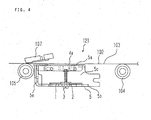
- FIG. 4 is a longitudinal sectional view of the antenna unit 121
- FIG. 5 is a perspective view showing a portion of the antenna unit 121
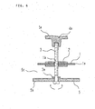
- FIG. 6 is a longitudinal sectional view of the same portion.
- the antenna 1 has a structure in which a support plate 1a supports a coil (not shown).
- the support plate 1a of the antenna 1 is arranged below (at the side of the platen) the label sheet 102 that is guided and transported on the sheet transporting path 103, and formed long in the widthwise direction of the label sheet 102.
- the mechanism for adjusting the distance provided to the antenna unit 121 is composed of a mechanism for elevating the support plate 1a of the antenna
- a pair of movable screws 3 is attached to the frame 5 so as to rotate about the axis of the movable screw 3, and the support plate 1a of the antenna 1 is attached to the movable screws 3.
- a pair of screw holes 1b is formed to the support plate 1a of the antenna 1 and the antenna fixing plates 2, and the movable screws 3 are screwed to the screw holes 1b.
- the movable screw 3 is rotatably provided to the frame 5 in such a manner that the movable screw 3 penetrates the lower member 5b of the frame 5 from below, and is prevented by a screw come-off preventing member 3a from coming off, and the leading end thereof is fitted to a boss 4a provided at the upper member 5a of the frame 5.
- An E-ring that can detachably be provided to the movable screw 3 is employed as the screw come-off preventing member 3a, for example. Therefore, in the example of the mechanism for adjusting the distance, by rotating the movable screws 3, the position of the antenna fixing plates 2 can be vertically moved by the screw action. Specifically, since the position of the antenna 1 changes to the sheet transporting path 103, the distance between the antenna 1 and the label sheet 102 can be changed.
- the distance between the antenna 1 and the label sheet 102a (or 102b), which is drawn from the rolled state and transported, can be adjusted depending upon the type of the label sheets 102a and 102b (tags 6a and 7a).
- the frequency band of RFID is UHF band
- 902 to 928 MHz can be used in the United States
- 866 to 870 MHz can be used inEurope.
- the usable frequencyband is different . Therefore, when the antenna 1 is attached to the position where data is always correctly written in the frequency of one district, the data might not correctly be written when the data is written to the tag having a frequency according to the other district.
- the frequency in which the data cannot be written is unallowable degree as an actual product.
- information can correctly be written to the tags 6a and 7a corresponding to various types of the label sheets 102a and 102b (tags 6a and 7a).
- FIG. 7 is an exploded perspective view of each section of the antenna unit 121.
- this antenna unit 121 either one of partitioning plates 8 and 9 formed of a sheet metal is provided at the middle position between the antenna 1 and the boss 4a.
- the partitioning plates 8 and 9 are formed with rectangular through-holes 8a and 9a at the central portion, respectively.
- the through-holes 8a and 9a are different from each other in size.
- the partitioning plates 8 and 9 are provided between the antenna 1 and the label sheet 102a or 102b that is drawn out from the rolled state to be transported on the sheet transporting path 103, and serves as a shielding member that blocks electric wave transmitted from the antenna 1 from reaching the position other than the target direction so as to limit the range of writing the information to the tags 6a and 7a by the antenna 1.
- the partitioning plate 8 or 9 is selected depending upon which one of the label sheet 102a and the label sheet 102b is used, whereby the narrow through-hole 8a or wide through-hole 9a can be selected, and hence, optimum information writing can be performed according to the type of the label sheet 102.
- the antenna fixing plates 2 are moved vertically by the screw action by rotating the antenna movable screws 3, as the structure for changing the position of the antenna 1.
- the antenna movable screws 3 may not be used, and a detachable structure for screwing the antenna fixing plates 2 for fixation at plural positions including the position relatively close to the transported label sheet 102 and the position relatively far from the transported label sheet 102 may be provided, whereby the antenna 1 is fixed to the position relatively close to the transported label sheet 102 or the position relatively far from the transported label sheet 102.
- the antenna 1 is attached close to the lower member 5b in the product for the United States, while the antenna 1 is attached close to the upper member 5a in the product for Europe.
- the optimum space between the attachment position of the antenna 1 in the product for the United States and the attachment position of the antenna 1 in the product for Europe is about 5 mm.
- the antenna 1 is attached to the close position generally in contact with the sheet transporting path 103 in the product for Europe, while the antenna 1 is attached to the position apart from the sheet transporting path 103 by about 5 mm in the product for the United States.
- the attachment position of the antenna 1 is determined according to the shape of the antenna 1. Specifically, since there are plural shapes of the antennas 1, the attachment position is determined according to the respective antennas 1, whereby the antenna 1 can easily be attached to the optimum attachment position.
Landscapes
- Engineering & Computer Science (AREA)
- Computer Networks & Wireless Communication (AREA)
- General Engineering & Computer Science (AREA)
- Physics & Mathematics (AREA)
- General Physics & Mathematics (AREA)
- Theoretical Computer Science (AREA)
- Accessory Devices And Overall Control Thereof (AREA)
- Labeling Devices (AREA)
- Support Of Aerials (AREA)
- Printers Characterized By Their Purpose (AREA)
- Electronic Switches (AREA)
Abstract
Description
- The present invention relates to a printer and an IC tag reading/writing apparatus that performs printing on a sheet or writes information to an IC tag serving as an IC chip and provided on this sheet.
- There has been known a label printer that performs printing on a label sheet, which is wound around a roll-type continuous sheet and is provided with an IC tag, and that writes information to the IC tag of this label sheet. The IC tag provided on the label sheet, which is the subject in the label printer, is generally an RF (Radio Frequency) tag, wherein information is wirelessly written and read. In order to wirelessly write and read data to and from the RF tag, an antenna is necessary to the label sheet provided with the RF tag and the reader/writer of the RF tag.
- Patent Reference 1:
Japanese Unexamined Patent Publication No. 2001-331768 - When information is written to the RF tag, there arises a problem that the information cannot be written well depending upon the difference in the frequency or the shape of the antenna, even if the position of the antenna in the label sheet and the position of the antenna of the reader/writer are the same.
- There is another problem that, if the length of the label sheet on the continuous sheet formed into a roll is short, the space between the RF tag on the label sheet and the RF tag provided on the adjacent label sheet becomes narrow. Specifically, data might be written on the RF tag on the label sheet that is not the target one, so that there is a problem that the type of the usable label sheet with the RF tag is naturally limited.
- In view of this, an object of the present invention is to provide a label printer, which performs printing to a label sheet provided with an IC tag and writes data to the IC tag, and which can cope with various types of label sheets.
- A label printer according to the present invention includes a print head that performs printing to a sheet provided with an IC chip; a transporting device that transports the sheet on a transporting path; an antenna that mediates data communication with the IC chip provided on the sheet transported on the transporting path; and a mechanism for adjusting a distance between the antenna and the transporting path.
-
- [FIG. 1] FIG. 1 is a longitudinal side view schematically showing a structure of a label printer according to one embodiment of the present invention.
- [FIG. 2] FIG. 2 is a plan view of a roll-type continuous sheet to which label sheets are attached.
- [FIG. 3] FIG. 3 is a plan view of a roll-type continuous sheet to which label sheets are attached, and.which is transported to the position of a thermal head and a platen roller.
- [FIG. 4] FIG. 4 is a longitudinal sectional view of a portion of an antenna unit in the label printer.
- [FIG. 5] FIG. 5 is a perspective view of the same portion.
- [FIG. 6] FIG. 6 is a longitudinal sectional view of the same portion.
- [FIG. 7] FIG. 7 is an exploded perspective view of each section of an RF tag reader/writer.
- One embodiment of the present invention will be explained with reference to FIGS. 1 to 7.
- FIG. 1 is a longitudinal side view schematically showing a structure of a
label printer 101. As shown in FIG. 1, arranged in thelabel printer 101 are atransport roller 104 that serves as a transporting device for drawing a label sheet, which is wound in a roll fashion, from the rolled state so as to transport thelabel sheet 102 on asheet transporting path 103, aplaten roller 105, anink ribbon 106, athermal head 107 that is arranged so as to oppose to theplaten roller 105 and prints predetermined items on thelabel sheet 102 with the use of theink ribbon 106, etc. Thethermal head 107 includes many resistance heat-generating members (not shown) arranged in a line. Theink ribbon 106 is inserted between thethermal head 107 and thelabel sheet 102. Thethermal head 107 is in pressed contact with theplaten roller 107, whereby the ink (not shown) on theink ribbon 106 is transferred onto thelabel sheet 102 by the heat of thethermal head 107. - On the
label printer 101, an RF tag reader/writer (not shown) is mounted that writes or reads information to or from RF (Radio Frequency)tags 6a and 7a (FIG. 2) provided on thelabel sheet 102 as an IC chip. The RF tag reader/writer is provided to an antenna unit 121 (FIG. 4), and connected to an antenna 1 that transmits and receives electric wave to thetags 6a and 7a (FIG. 2). Theantenna unit 121 described above is arranged in the vicinity of the upstream side of thethermal head 107 in the transporting direction of thelabel sheet 102 and at the downstream side with respect to thetransport roller 104. - FIG. 2 is a plan view of the
label sheet 102, and FIG. 3 is a plan view showing a positional relationship of thelabel sheet 102 that is transported to thethermal head 107 and theplaten roller 105 by thetransport roller 104. FIG. 2(a) and FIG. 2(b) respectively illustrate alabel sheet 102 having a different size, whereinlabel sheets continuous sheets 6 and 7 wound in a rolled fashion.Numerals 6a and 7a are RF tags formed on thelabel sheets - Subsequently, the
antenna unit 121 will be explained. FIG. 4 is a longitudinal sectional view of theantenna unit 121, FIG. 5 is a perspective view showing a portion of theantenna unit 121, and FIG. 6 is a longitudinal sectional view of the same portion. - A mechanism for adjusting the distance between the antenna 1 provided to the
antenna unit 121 and thesheet transporting path 103 will be explained. The antenna 1 has a structure in which a support plate 1a supports a coil (not shown). The support plate 1a of the antenna 1 is arranged below (at the side of the platen) thelabel sheet 102 that is guided and transported on thesheet transporting path 103, and formed long in the widthwise direction of thelabel sheet 102. The mechanism for adjusting the distance provided to theantenna unit 121 is composed of a mechanism for elevating the support plate 1a of the antenna - 1. Specifically,
antenna fixing plates 2 are fixed to both ends of the support plate 1a. Theantenna fixing plates 2 are configured such that two plates are opposite to each other with a gap capable of sandwiching the support plate 1a of the antenna 1, and have a slit shape in which the side opposite to the side of sandwiching the support plate 1a is closed. Since theantenna fixing plates 2 having the slit shape hold both ends of the support plate 1a in the widthwise direction of thelabel sheet 102, theantenna fixing plates 2 are fixed to the support plate 1a. Theantenna unit 121 has aframe 5 that forms aspace 5c between anupper member 5a and alower member 5b. Further, an opening 5d is formed on theupper member 5a and thelower member 5b of theframe 5 as shown in FIG. 7. A risingmember 5e that is formed by bending a metal plate from thelower member 5b and serves as a second shielding member is formed at theframe 5 at the side of the platen. This risingmember 5e is provided in order to prevent data from being written again after the printing onto the label sheet on which data has already been written. - A pair of
movable screws 3 is attached to theframe 5 so as to rotate about the axis of themovable screw 3, and the support plate 1a of the antenna 1 is attached to themovable screws 3. Specifically, a pair ofscrew holes 1b is formed to the support plate 1a of the antenna 1 and theantenna fixing plates 2, and themovable screws 3 are screwed to thescrew holes 1b. Themovable screw 3 is rotatably provided to theframe 5 in such a manner that themovable screw 3 penetrates thelower member 5b of theframe 5 from below, and is prevented by a screw come-off preventingmember 3a from coming off, and the leading end thereof is fitted to aboss 4a provided at theupper member 5a of theframe 5. An E-ring that can detachably be provided to themovable screw 3 is employed as the screw come-off preventingmember 3a, for example. Therefore, in the example of the mechanism for adjusting the distance, by rotating themovable screws 3, the position of theantenna fixing plates 2 can be vertically moved by the screw action. Specifically, since the position of the antenna 1 changes to thesheet transporting path 103, the distance between the antenna 1 and thelabel sheet 102 can be changed. - With this mechanism, the distance between the antenna 1 and the
label sheet 102a (or 102b), which is drawn from the rolled state and transported, can be adjusted depending upon the type of thelabel sheets tags 6a and 7a). For example, even if the frequency band of RFID is UHF band, 902 to 928 MHz can be used in the United States, and 866 to 870 MHz can be used inEurope. In other words, the usable frequencyband is different . Therefore, when the antenna 1 is attached to the position where data is always correctly written in the frequency of one district, the data might not correctly be written when the data is written to the tag having a frequency according to the other district. The frequency in which the data cannot be written is unallowable degree as an actual product. However, according to one embodiment for solving this problem, information can correctly be written to thetags 6a and 7a corresponding to various types of thelabel sheets tags 6a and 7a). - FIG. 7 is an exploded perspective view of each section of the
antenna unit 121. In thisantenna unit 121, either one of partitioning plates 8 and 9 formed of a sheet metal is provided at the middle position between the antenna 1 and theboss 4a. The partitioning plates 8 and 9 are formed with rectangular through-holes holes label sheet sheet transporting path 103, and serves as a shielding member that blocks electric wave transmitted from the antenna 1 from reaching the position other than the target direction so as to limit the range of writing the information to thetags 6a and 7a by the antenna 1. - Specifically, only the electric wave passing through the through-
holes tags 6a and 7a, so that there is no chance that the information is written to anotherlabel sheet - The partitioning plate 8 or 9 is selected depending upon which one of the
label sheet 102a and thelabel sheet 102b is used, whereby the narrow through-hole 8a or wide through-hole 9a can be selected, and hence, optimum information writing can be performed according to the type of thelabel sheet 102. - In one embodiment described above, the
antenna fixing plates 2 are moved vertically by the screw action by rotating the antennamovable screws 3, as the structure for changing the position of the antenna 1. However, the antennamovable screws 3 may not be used, and a detachable structure for screwing theantenna fixing plates 2 for fixation at plural positions including the position relatively close to the transportedlabel sheet 102 and the position relatively far from the transportedlabel sheet 102 may be provided, whereby the antenna 1 is fixed to the position relatively close to the transportedlabel sheet 102 or the position relatively far from the transportedlabel sheet 102. - In the case of the aforesaid UHF band, the antenna 1 is attached close to the
lower member 5b in the product for the United States, while the antenna 1 is attached close to theupper member 5a in the product for Europe. The optimum space between the attachment position of the antenna 1 in the product for the United States and the attachment position of the antenna 1 in the product for Europe is about 5 mm. Specifically, the antenna 1 is attached to the close position generally in contact with thesheet transporting path 103 in the product for Europe, while the antenna 1 is attached to the position apart from thesheet transporting path 103 by about 5 mm in the product for the United States. - The shape of the antenna 1 is not specifically described in the present application, but the shape of the antenna 1 varies since the frequency to be handled is different. Therefore, in the present embodiment, the attachment position of the antenna 1 is determined according to the shape of the antenna 1. Specifically, since there are plural shapes of the antennas 1, the attachment position is determined according to the respective antennas 1, whereby the antenna 1 can easily be attached to the optimum attachment position.
Claims (14)
- A printer comprising:a print head that performs printing to a sheet provided with an IC chip;a transporting device that transports the sheet on a transporting path;an antenna that mediates data communication with the IC chip provided on the sheet transported on the transporting path; anda mechanism for adjusting a distance between the antenna and the transporting path.
- The printer according to claim 1, further comprising a shielding member that is provided between the antenna and the transporting path, and shields an electric wave transmitted from the antenna, to limit the data communication range of the antenna to the IC chip.
- The printer according to claim 1, further comprising a second shielding member that is provided between the antenna and the position at the downstream side of the transporting path, to shield an electric wave transmitted from the antenna.
- The printer according to claim 2 and claim 3, further comprising a metallic frame that includes: an upper member, which has an opening through which the electric wave from the antenna passes and forms a part of the transporting path; and a lower member, which is positioned below the upper member via a space into which the antenna is positioned, the metallic frame being arranged at the upstream side of the transporting path with respect to the print head,
wherein:the shielding member is made of a metal plate that is provided integral with the upper member and has a through-hole through which an electric wave passes; andthe second shielding member is made of a part of the frame. - The printer according to claim 4, wherein the upper member detachably holds plural types of the shielding member in which the size of the through-hole formed on the metal plate is different.
- The printer according to claim 4, wherein the lower member has an opening at the position facing the antenna.
- The printer according to claim 1, wherein the mechanism for adjusting the distance includes:a support plate for supporting the antenna;a screw hole formed on the support plate; anda movable screw that is arranged so as to direct an axial direction to a distance adjusting direction between the antenna and the transporting path, and screwed to the screw hole.
- The printer according to claim 7, wherein the support plate has an antenna fixing plate at the portion of the screw hole.
- The printer according to claim 1, wherein the mechanism for adjusting the distance includes:a support plate for supporting the antenna; anda structure in which the support plate is detachably attached at plural attachment positions for varying the distance between the antenna and the transporting path.
- The printer according to claim 1, wherein the print head is a line-type thermal head that is in contact with a platen roller via the transporting path.
- The printer according to claim 10, wherein the thermal head is arranged at the downstream side of the transporting path with respect to the antenna.
- The printer according to claim 10, wherein:the transporting device has a pair of transport rollers that are in contact with each other via the transporting path at the upstream side of the transporting path with respect to the platen, at least one of the pair of transport rollers being rotatably driven; andthe antenna is arranged between the transport roller and the platen roller.
- The printer according to claim 1, wherein the sheet is a label sheet having plural labels attached onto a pasteboard and wound in a rolled fashion.
- An IC chip communication apparatus comprising:an antenna that mediates data communication with an IC chip provided on a sheet;a transporting device that guides and transports the sheet to the position where the antenna mediates the data communication with the IC chip; anda mechanism for adjusting a distance that adjusts a distance between the antenna and the transporting path.
Applications Claiming Priority (2)
| Application Number | Priority Date | Filing Date | Title |
|---|---|---|---|
| JP2005059103 | 2005-03-03 | ||
| PCT/JP2006/303965 WO2006093219A1 (en) | 2005-03-03 | 2006-03-02 | Printer and ic chip communication device |
Publications (3)
| Publication Number | Publication Date |
|---|---|
| EP1854637A1 true EP1854637A1 (en) | 2007-11-14 |
| EP1854637A4 EP1854637A4 (en) | 2009-05-06 |
| EP1854637B1 EP1854637B1 (en) | 2011-03-02 |
Family
ID=36941248
Family Applications (1)
| Application Number | Title | Priority Date | Filing Date |
|---|---|---|---|
| EP06715074A Expired - Lifetime EP1854637B1 (en) | 2005-03-03 | 2006-03-02 | Printer and ic chip communication device |
Country Status (6)
| Country | Link |
|---|---|
| US (2) | US7926722B2 (en) |
| EP (1) | EP1854637B1 (en) |
| JP (1) | JPWO2006093219A1 (en) |
| CN (1) | CN101132929A (en) |
| DE (1) | DE602006020415D1 (en) |
| WO (1) | WO2006093219A1 (en) |
Cited By (2)
| Publication number | Priority date | Publication date | Assignee | Title |
|---|---|---|---|---|
| WO2010151434A1 (en) * | 2009-06-26 | 2010-12-29 | Premark Feg L.L.C. | Printer and scale for handling rfid labels |
| US8600819B2 (en) | 2003-06-27 | 2013-12-03 | Premark FEG. L.L.C. | Food product scale and related in-store random weight item transaction system with RFID |
Families Citing this family (7)
| Publication number | Priority date | Publication date | Assignee | Title |
|---|---|---|---|---|
| JP2007293714A (en) * | 2006-04-26 | 2007-11-08 | Toshiba Tec Corp | Wireless communication apparatus and printing apparatus |
| JP2010079594A (en) * | 2008-09-26 | 2010-04-08 | Nec Personal Products Co Ltd | Rfid printer |
| JP2010206323A (en) * | 2009-02-27 | 2010-09-16 | Toshiba Tec Corp | Rfid printer |
| JP5450197B2 (en) * | 2010-03-25 | 2014-03-26 | 沖電気工業株式会社 | Non-contact reading / writing device |
| JP6225763B2 (en) * | 2014-03-12 | 2017-11-08 | ブラザー工業株式会社 | Image forming apparatus |
| JP6698459B2 (en) * | 2016-07-25 | 2020-05-27 | サトーホールディングス株式会社 | Printer |
| CN217279580U (en) * | 2021-11-22 | 2022-08-23 | 手持产品公司 | Radio frequency identification printer with rotatable antenna support member |
Family Cites Families (17)
| Publication number | Priority date | Publication date | Assignee | Title |
|---|---|---|---|---|
| US6104291A (en) * | 1998-01-09 | 2000-08-15 | Intermec Ip Corp. | Method and apparatus for testing RFID tags |
| DE19846295B4 (en) * | 1998-10-07 | 2008-04-24 | Kabushiki Kaisha Sato | Printer with a device for driving transponder chips |
| US6246326B1 (en) * | 1999-05-05 | 2001-06-12 | Intermec Ip Corp. | Performance optimized smart label printer |
| JP4545280B2 (en) * | 2000-05-24 | 2010-09-15 | 株式会社サトー | Printer |
| JP4514374B2 (en) * | 2001-09-05 | 2010-07-28 | トッパン・フォームズ株式会社 | RF-ID inspection system |
| JP4845306B2 (en) * | 2001-09-25 | 2011-12-28 | トッパン・フォームズ株式会社 | RF-ID inspection system |
| WO2003036760A1 (en) * | 2001-10-22 | 2003-05-01 | Sumida Corporation | Antenna coil and transmission antenna |
| JP2003300356A (en) | 2002-04-09 | 2003-10-21 | Canon Finetech Inc | Recording device |
| GB2395462B (en) * | 2002-11-21 | 2006-04-05 | Hewlett Packard Co | Apparatus for printing and memory tag application and method therefor |
| JP4268514B2 (en) * | 2003-12-25 | 2009-05-27 | 東芝テック株式会社 | Wireless tag issuing device |
| US7561022B2 (en) * | 2004-01-13 | 2009-07-14 | George Schmitt & Company, Inc. | System and method for validating radio frequency identification tags |
| JP3935162B2 (en) * | 2004-04-28 | 2007-06-20 | 東芝テック株式会社 | RF tag reader / writer and printer |
| US7439858B2 (en) * | 2004-06-22 | 2008-10-21 | Paxar Americas, Inc. | RFID printer and antennas |
| US20060071063A1 (en) * | 2004-09-29 | 2006-04-06 | Duckett Jeanne F | RFID printer system, method of printing and sets of record members |
| US20070100710A1 (en) * | 2005-11-01 | 2007-05-03 | Moneet Singh | System and methods for m-commerce transactions |
| JP4394147B2 (en) * | 2006-02-06 | 2010-01-06 | 三菱電機株式会社 | High frequency module |
| US7824118B2 (en) * | 2006-04-25 | 2010-11-02 | Toshiba Tec Kabushiki Kaisha | Printer comprising a flexible member extending over the antennas of RFID labels wound on a roll |
-
2006
- 2006-03-02 US US11/884,630 patent/US7926722B2/en not_active Expired - Fee Related
- 2006-03-02 WO PCT/JP2006/303965 patent/WO2006093219A1/en not_active Ceased
- 2006-03-02 EP EP06715074A patent/EP1854637B1/en not_active Expired - Lifetime
- 2006-03-02 JP JP2007505997A patent/JPWO2006093219A1/en active Pending
- 2006-03-02 CN CNA2006800069871A patent/CN101132929A/en active Pending
- 2006-03-02 DE DE602006020415T patent/DE602006020415D1/en not_active Expired - Lifetime
-
2011
- 2011-03-09 US US13/044,444 patent/US20110155807A1/en not_active Abandoned
Cited By (3)
| Publication number | Priority date | Publication date | Assignee | Title |
|---|---|---|---|---|
| US8600819B2 (en) | 2003-06-27 | 2013-12-03 | Premark FEG. L.L.C. | Food product scale and related in-store random weight item transaction system with RFID |
| WO2010151434A1 (en) * | 2009-06-26 | 2010-12-29 | Premark Feg L.L.C. | Printer and scale for handling rfid labels |
| US8432567B2 (en) | 2009-06-26 | 2013-04-30 | Premark Feg L.L.C. | Printer and scale for handling RFID labels |
Also Published As
| Publication number | Publication date |
|---|---|
| US20110155807A1 (en) | 2011-06-30 |
| CN101132929A (en) | 2008-02-27 |
| WO2006093219A1 (en) | 2006-09-08 |
| EP1854637B1 (en) | 2011-03-02 |
| EP1854637A4 (en) | 2009-05-06 |
| JPWO2006093219A1 (en) | 2008-08-07 |
| US7926722B2 (en) | 2011-04-19 |
| US20080257964A1 (en) | 2008-10-23 |
| DE602006020415D1 (en) | 2011-04-14 |
Similar Documents
| Publication | Publication Date | Title |
|---|---|---|
| US20110155807A1 (en) | Printer and ic chip communication apparatus | |
| US8160493B2 (en) | Spatially selective UHF near field microstrip coupler device and RFID systems using device | |
| US6848616B2 (en) | System and method for selective communication with RFID transponders | |
| US7824118B2 (en) | Printer comprising a flexible member extending over the antennas of RFID labels wound on a roll | |
| EP1591946B1 (en) | RF tag reader/writer and printer containing the RF tag reader/writer | |
| EP4382302B1 (en) | Printing apparatus | |
| JP4745987B2 (en) | Printer | |
| JP2015194815A (en) | Ic tag issuing device and shield plate | |
| JP2006018456A (en) | Printer | |
| JP2015123615A (en) | Rfid tag issuing device | |
| JP7619121B2 (en) | Wireless tag information writer | |
| JP2008262344A (en) | RFID paper printer | |
| JP6200332B2 (en) | RF tag reader / writer | |
| JP6124830B2 (en) | IC tag issuing device and IC tag issuing method | |
| JP6577619B2 (en) | IC tag issuing device and shield plate | |
| JP4705507B2 (en) | RFID printer | |
| US20260037754A1 (en) | Rfid coupler and associated rfid enabled device | |
| JP2005161574A (en) | RFID printer paper printer | |
| JP2016117231A (en) | Passbook | |
| JP2010079594A (en) | Rfid printer | |
| TWM564526U (en) | Printer with RFID tag automatic correction system |
Legal Events
| Date | Code | Title | Description |
|---|---|---|---|
| PUAI | Public reference made under article 153(3) epc to a published international application that has entered the european phase |
Free format text: ORIGINAL CODE: 0009012 |
|
| 17P | Request for examination filed |
Effective date: 20070822 |
|
| AK | Designated contracting states |
Kind code of ref document: A1 Designated state(s): BE DE ES FR GB NL |
|
| DAX | Request for extension of the european patent (deleted) | ||
| RBV | Designated contracting states (corrected) |
Designated state(s): BE DE ES FR GB NL |
|
| A4 | Supplementary search report drawn up and despatched |
Effective date: 20090403 |
|
| 17Q | First examination report despatched |
Effective date: 20090821 |
|
| GRAP | Despatch of communication of intention to grant a patent |
Free format text: ORIGINAL CODE: EPIDOSNIGR1 |
|
| GRAS | Grant fee paid |
Free format text: ORIGINAL CODE: EPIDOSNIGR3 |
|
| GRAA | (expected) grant |
Free format text: ORIGINAL CODE: 0009210 |
|
| AK | Designated contracting states |
Kind code of ref document: B1 Designated state(s): BE DE ES FR GB NL |
|
| REG | Reference to a national code |
Ref country code: GB Ref legal event code: FG4D |
|
| REF | Corresponds to: |
Ref document number: 602006020415 Country of ref document: DE Date of ref document: 20110414 Kind code of ref document: P |
|
| REG | Reference to a national code |
Ref country code: DE Ref legal event code: R096 Ref document number: 602006020415 Country of ref document: DE Effective date: 20110414 |
|
| PGFP | Annual fee paid to national office [announced via postgrant information from national office to epo] |
Ref country code: NL Payment date: 20110331 Year of fee payment: 6 |
|
| REG | Reference to a national code |
Ref country code: NL Ref legal event code: VDEP Effective date: 20110302 |
|
| PG25 | Lapsed in a contracting state [announced via postgrant information from national office to epo] |
Ref country code: ES Free format text: LAPSE BECAUSE OF FAILURE TO SUBMIT A TRANSLATION OF THE DESCRIPTION OR TO PAY THE FEE WITHIN THE PRESCRIBED TIME-LIMIT Effective date: 20110613 |
|
| PGFP | Annual fee paid to national office [announced via postgrant information from national office to epo] |
Ref country code: GB Payment date: 20110316 Year of fee payment: 6 Ref country code: ES Payment date: 20110330 Year of fee payment: 6 Ref country code: FR Payment date: 20110629 Year of fee payment: 6 Ref country code: DE Payment date: 20110316 Year of fee payment: 6 Ref country code: BE Payment date: 20110311 Year of fee payment: 6 |
|
| PG25 | Lapsed in a contracting state [announced via postgrant information from national office to epo] |
Ref country code: NL Free format text: LAPSE BECAUSE OF FAILURE TO SUBMIT A TRANSLATION OF THE DESCRIPTION OR TO PAY THE FEE WITHIN THE PRESCRIBED TIME-LIMIT Effective date: 20110302 |
|
| PLBE | No opposition filed within time limit |
Free format text: ORIGINAL CODE: 0009261 |
|
| STAA | Information on the status of an ep patent application or granted ep patent |
Free format text: STATUS: NO OPPOSITION FILED WITHIN TIME LIMIT |
|
| 26N | No opposition filed |
Effective date: 20111205 |
|
| REG | Reference to a national code |
Ref country code: DE Ref legal event code: R097 Ref document number: 602006020415 Country of ref document: DE Effective date: 20111205 |
|
| GBPC | Gb: european patent ceased through non-payment of renewal fee |
Effective date: 20120302 |
|
| REG | Reference to a national code |
Ref country code: FR Ref legal event code: ST Effective date: 20121130 |
|
| PG25 | Lapsed in a contracting state [announced via postgrant information from national office to epo] |
Ref country code: FR Free format text: LAPSE BECAUSE OF NON-PAYMENT OF DUE FEES Effective date: 20120402 Ref country code: GB Free format text: LAPSE BECAUSE OF NON-PAYMENT OF DUE FEES Effective date: 20120302 |
|
| REG | Reference to a national code |
Ref country code: DE Ref legal event code: R119 Ref document number: 602006020415 Country of ref document: DE Effective date: 20121002 |
|
| PG25 | Lapsed in a contracting state [announced via postgrant information from national office to epo] |
Ref country code: DE Free format text: LAPSE BECAUSE OF NON-PAYMENT OF DUE FEES Effective date: 20121002 |
|
| PG25 | Lapsed in a contracting state [announced via postgrant information from national office to epo] |
Ref country code: BE Free format text: THE PATENT HAS BEEN ANNULLED BY A DECISION OF A NATIONAL AUTHORITY Effective date: 20110302 |