EP1850169A1 - Liquid crystal panel - Google Patents
Liquid crystal panel Download PDFInfo
- Publication number
- EP1850169A1 EP1850169A1 EP07008014A EP07008014A EP1850169A1 EP 1850169 A1 EP1850169 A1 EP 1850169A1 EP 07008014 A EP07008014 A EP 07008014A EP 07008014 A EP07008014 A EP 07008014A EP 1850169 A1 EP1850169 A1 EP 1850169A1
- Authority
- EP
- European Patent Office
- Prior art keywords
- liquid crystal
- group
- polarizing plate
- optical compensation
- crystal panel
- Prior art date
- Legal status (The legal status is an assumption and is not a legal conclusion. Google has not performed a legal analysis and makes no representation as to the accuracy of the status listed.)
- Withdrawn
Links
- 239000004973 liquid crystal related substance Substances 0.000 title claims abstract description 189
- XLYOFNOQVPJJNP-UHFFFAOYSA-N water Substances O XLYOFNOQVPJJNP-UHFFFAOYSA-N 0.000 claims abstract description 17
- 210000002858 crystal cell Anatomy 0.000 claims description 43
- 239000003795 chemical substances by application Substances 0.000 abstract description 26
- 229910052731 fluorine Inorganic materials 0.000 abstract description 20
- 239000011737 fluorine Substances 0.000 abstract description 16
- 125000001153 fluoro group Chemical group F* 0.000 abstract description 4
- 239000010410 layer Substances 0.000 description 141
- 230000003287 optical effect Effects 0.000 description 124
- 239000010408 film Substances 0.000 description 67
- 239000011241 protective layer Substances 0.000 description 47
- 125000004432 carbon atom Chemical group C* 0.000 description 39
- 125000000217 alkyl group Chemical group 0.000 description 36
- 238000005259 measurement Methods 0.000 description 29
- 239000000758 substrate Substances 0.000 description 29
- GTDPSWPPOUPBNX-UHFFFAOYSA-N ac1mqpva Chemical compound CC12C(=O)OC(=O)C1(C)C1(C)C2(C)C(=O)OC1=O GTDPSWPPOUPBNX-UHFFFAOYSA-N 0.000 description 26
- 238000000034 method Methods 0.000 description 26
- 229920005989 resin Polymers 0.000 description 24
- 239000011347 resin Substances 0.000 description 24
- -1 ethylene glycol fatty ester Chemical class 0.000 description 21
- 125000001997 phenyl group Chemical group [H]C1=C([H])C([H])=C(*)C([H])=C1[H] 0.000 description 21
- 229920001721 polyimide Polymers 0.000 description 21
- 239000004642 Polyimide Substances 0.000 description 20
- 239000000463 material Substances 0.000 description 19
- 239000004925 Acrylic resin Substances 0.000 description 17
- 229920002678 cellulose Polymers 0.000 description 17
- 229910052736 halogen Inorganic materials 0.000 description 17
- 150000002367 halogens Chemical class 0.000 description 17
- 239000000243 solution Substances 0.000 description 17
- 125000001424 substituent group Chemical group 0.000 description 17
- 229920000178 Acrylic resin Polymers 0.000 description 16
- YCKRFDGAMUMZLT-UHFFFAOYSA-N Fluorine atom Chemical compound [F] YCKRFDGAMUMZLT-UHFFFAOYSA-N 0.000 description 15
- 125000003118 aryl group Chemical group 0.000 description 15
- 239000001913 cellulose Substances 0.000 description 15
- 229920006254 polymer film Polymers 0.000 description 14
- 239000004372 Polyvinyl alcohol Substances 0.000 description 13
- 230000000052 comparative effect Effects 0.000 description 13
- 229920002451 polyvinyl alcohol Polymers 0.000 description 13
- 239000002904 solvent Substances 0.000 description 13
- 238000006467 substitution reaction Methods 0.000 description 13
- 229920002284 Cellulose triacetate Polymers 0.000 description 12
- NNLVGZFZQQXQNW-ADJNRHBOSA-N [(2r,3r,4s,5r,6s)-4,5-diacetyloxy-3-[(2s,3r,4s,5r,6r)-3,4,5-triacetyloxy-6-(acetyloxymethyl)oxan-2-yl]oxy-6-[(2r,3r,4s,5r,6s)-4,5,6-triacetyloxy-2-(acetyloxymethyl)oxan-3-yl]oxyoxan-2-yl]methyl acetate Chemical compound O([C@@H]1O[C@@H]([C@H]([C@H](OC(C)=O)[C@H]1OC(C)=O)O[C@H]1[C@@H]([C@@H](OC(C)=O)[C@H](OC(C)=O)[C@@H](COC(C)=O)O1)OC(C)=O)COC(=O)C)[C@@H]1[C@@H](COC(C)=O)O[C@@H](OC(C)=O)[C@H](OC(C)=O)[C@H]1OC(C)=O NNLVGZFZQQXQNW-ADJNRHBOSA-N 0.000 description 12
- 125000003545 alkoxy group Chemical group 0.000 description 11
- 125000004435 hydrogen atom Chemical class [H]* 0.000 description 11
- 229920000642 polymer Polymers 0.000 description 11
- ZCYVEMRRCGMTRW-UHFFFAOYSA-N 7553-56-2 Chemical compound [I] ZCYVEMRRCGMTRW-UHFFFAOYSA-N 0.000 description 10
- 238000010521 absorption reaction Methods 0.000 description 10
- 230000000694 effects Effects 0.000 description 10
- 229910052740 iodine Inorganic materials 0.000 description 10
- ZWEHNKRNPOVVGH-UHFFFAOYSA-N 2-Butanone Chemical compound CCC(C)=O ZWEHNKRNPOVVGH-UHFFFAOYSA-N 0.000 description 9
- NIXOWILDQLNWCW-UHFFFAOYSA-N acrylic acid group Chemical group C(C=C)(=O)O NIXOWILDQLNWCW-UHFFFAOYSA-N 0.000 description 9
- 229910052739 hydrogen Inorganic materials 0.000 description 9
- 239000001257 hydrogen Substances 0.000 description 9
- 239000011630 iodine Substances 0.000 description 9
- 238000006116 polymerization reaction Methods 0.000 description 9
- 125000001501 propionyl group Chemical group O=C([*])C([H])([H])C([H])([H])[H] 0.000 description 8
- 239000004952 Polyamide Substances 0.000 description 7
- 238000001035 drying Methods 0.000 description 7
- LYCAIKOWRPUZTN-UHFFFAOYSA-N ethylene glycol Natural products OCCO LYCAIKOWRPUZTN-UHFFFAOYSA-N 0.000 description 7
- 239000007788 liquid Substances 0.000 description 7
- 230000010287 polarization Effects 0.000 description 7
- 229920002647 polyamide Polymers 0.000 description 7
- 125000006158 tetracarboxylic acid group Chemical group 0.000 description 7
- RTZKZFJDLAIYFH-UHFFFAOYSA-N Diethyl ether Chemical compound CCOCC RTZKZFJDLAIYFH-UHFFFAOYSA-N 0.000 description 6
- 229920000106 Liquid crystal polymer Polymers 0.000 description 6
- 229910052801 chlorine Inorganic materials 0.000 description 6
- 238000004040 coloring Methods 0.000 description 6
- BGTOWKSIORTVQH-UHFFFAOYSA-N cyclopentanone Chemical compound O=C1CCCC1 BGTOWKSIORTVQH-UHFFFAOYSA-N 0.000 description 6
- 229920000728 polyester Polymers 0.000 description 6
- NLKNQRATVPKPDG-UHFFFAOYSA-M potassium iodide Chemical compound [K+].[I-] NLKNQRATVPKPDG-UHFFFAOYSA-M 0.000 description 6
- 239000004820 Pressure-sensitive adhesive Substances 0.000 description 5
- 125000000218 acetic acid group Chemical group C(C)(=O)* 0.000 description 5
- 239000000853 adhesive Substances 0.000 description 5
- 230000001070 adhesive effect Effects 0.000 description 5
- 239000000460 chlorine Substances 0.000 description 5
- 125000005843 halogen group Chemical group 0.000 description 5
- 238000003475 lamination Methods 0.000 description 5
- 125000002496 methyl group Chemical group [H]C([H])([H])* 0.000 description 5
- 239000000203 mixture Substances 0.000 description 5
- 239000004014 plasticizer Substances 0.000 description 5
- 229920006260 polyaryletherketone Polymers 0.000 description 5
- GEYOCULIXLDCMW-UHFFFAOYSA-N 1,2-phenylenediamine Chemical compound NC1=CC=CC=C1N GEYOCULIXLDCMW-UHFFFAOYSA-N 0.000 description 4
- VLDPXPPHXDGHEW-UHFFFAOYSA-N 1-chloro-2-dichlorophosphoryloxybenzene Chemical compound ClC1=CC=CC=C1OP(Cl)(Cl)=O VLDPXPPHXDGHEW-UHFFFAOYSA-N 0.000 description 4
- NVKGJHAQGWCWDI-UHFFFAOYSA-N 4-[4-amino-2-(trifluoromethyl)phenyl]-3-(trifluoromethyl)aniline Chemical group FC(F)(F)C1=CC(N)=CC=C1C1=CC=C(N)C=C1C(F)(F)F NVKGJHAQGWCWDI-UHFFFAOYSA-N 0.000 description 4
- QTBSBXVTEAMEQO-UHFFFAOYSA-N Acetic acid Natural products CC(O)=O QTBSBXVTEAMEQO-UHFFFAOYSA-N 0.000 description 4
- WKBOTKDWSSQWDR-UHFFFAOYSA-N Bromine atom Chemical compound [Br] WKBOTKDWSSQWDR-UHFFFAOYSA-N 0.000 description 4
- ZAMOUSCENKQFHK-UHFFFAOYSA-N Chlorine atom Chemical compound [Cl] ZAMOUSCENKQFHK-UHFFFAOYSA-N 0.000 description 4
- NTIZESTWPVYFNL-UHFFFAOYSA-N Methyl isobutyl ketone Chemical compound CC(C)CC(C)=O NTIZESTWPVYFNL-UHFFFAOYSA-N 0.000 description 4
- UIHCLUNTQKBZGK-UHFFFAOYSA-N Methyl isobutyl ketone Natural products CCC(C)C(C)=O UIHCLUNTQKBZGK-UHFFFAOYSA-N 0.000 description 4
- ISWSIDIOOBJBQZ-UHFFFAOYSA-N Phenol Chemical compound OC1=CC=CC=C1 ISWSIDIOOBJBQZ-UHFFFAOYSA-N 0.000 description 4
- 125000002777 acetyl group Chemical group [H]C([H])([H])C(*)=O 0.000 description 4
- MWPLVEDNUUSJAV-UHFFFAOYSA-N anthracene Chemical compound C1=CC=CC2=CC3=CC=CC=C3C=C21 MWPLVEDNUUSJAV-UHFFFAOYSA-N 0.000 description 4
- 239000007864 aqueous solution Substances 0.000 description 4
- 150000004984 aromatic diamines Chemical class 0.000 description 4
- 125000006615 aromatic heterocyclic group Chemical group 0.000 description 4
- 229920001577 copolymer Polymers 0.000 description 4
- 239000002178 crystalline material Substances 0.000 description 4
- NIHNNTQXNPWCJQ-UHFFFAOYSA-N fluorene Chemical compound C1=CC=C2CC3=CC=CC=C3C2=C1 NIHNNTQXNPWCJQ-UHFFFAOYSA-N 0.000 description 4
- VANNPISTIUFMLH-UHFFFAOYSA-N glutaric anhydride Chemical group O=C1CCCC(=O)O1 VANNPISTIUFMLH-UHFFFAOYSA-N 0.000 description 4
- JFNLZVQOOSMTJK-KNVOCYPGSA-N norbornene Chemical compound C1[C@@H]2CC[C@H]1C=C2 JFNLZVQOOSMTJK-KNVOCYPGSA-N 0.000 description 4
- 125000004430 oxygen atom Chemical group O* 0.000 description 4
- 230000001681 protective effect Effects 0.000 description 4
- 239000011342 resin composition Substances 0.000 description 4
- 125000000547 substituted alkyl group Chemical group 0.000 description 4
- 229920005992 thermoplastic resin Polymers 0.000 description 4
- 239000010409 thin film Substances 0.000 description 4
- VQVIHDPBMFABCQ-UHFFFAOYSA-N 5-(1,3-dioxo-2-benzofuran-5-carbonyl)-2-benzofuran-1,3-dione Chemical compound C1=C2C(=O)OC(=O)C2=CC(C(C=2C=C3C(=O)OC(=O)C3=CC=2)=O)=C1 VQVIHDPBMFABCQ-UHFFFAOYSA-N 0.000 description 3
- WFDIJRYMOXRFFG-UHFFFAOYSA-N Acetic anhydride Chemical compound CC(=O)OC(C)=O WFDIJRYMOXRFFG-UHFFFAOYSA-N 0.000 description 3
- CSCPPACGZOOCGX-UHFFFAOYSA-N Acetone Chemical compound CC(C)=O CSCPPACGZOOCGX-UHFFFAOYSA-N 0.000 description 3
- WEVYAHXRMPXWCK-UHFFFAOYSA-N Acetonitrile Chemical compound CC#N WEVYAHXRMPXWCK-UHFFFAOYSA-N 0.000 description 3
- UHOVQNZJYSORNB-UHFFFAOYSA-N Benzene Chemical compound C1=CC=CC=C1 UHOVQNZJYSORNB-UHFFFAOYSA-N 0.000 description 3
- QGJOPFRUJISHPQ-UHFFFAOYSA-N Carbon disulfide Chemical compound S=C=S QGJOPFRUJISHPQ-UHFFFAOYSA-N 0.000 description 3
- YMWUJEATGCHHMB-UHFFFAOYSA-N Dichloromethane Chemical compound ClCCl YMWUJEATGCHHMB-UHFFFAOYSA-N 0.000 description 3
- XEKOWRVHYACXOJ-UHFFFAOYSA-N Ethyl acetate Chemical compound CCOC(C)=O XEKOWRVHYACXOJ-UHFFFAOYSA-N 0.000 description 3
- ZMXDDKWLCZADIW-UHFFFAOYSA-N N,N-Dimethylformamide Chemical compound CN(C)C=O ZMXDDKWLCZADIW-UHFFFAOYSA-N 0.000 description 3
- 239000004743 Polypropylene Substances 0.000 description 3
- DNIAPMSPPWPWGF-UHFFFAOYSA-N Propylene glycol Chemical compound CC(O)CO DNIAPMSPPWPWGF-UHFFFAOYSA-N 0.000 description 3
- HEMHJVSKTPXQMS-UHFFFAOYSA-M Sodium hydroxide Chemical compound [OH-].[Na+] HEMHJVSKTPXQMS-UHFFFAOYSA-M 0.000 description 3
- YXFVVABEGXRONW-UHFFFAOYSA-N Toluene Chemical compound CC1=CC=CC=C1 YXFVVABEGXRONW-UHFFFAOYSA-N 0.000 description 3
- 125000001931 aliphatic group Chemical group 0.000 description 3
- 239000003513 alkali Substances 0.000 description 3
- 230000015572 biosynthetic process Effects 0.000 description 3
- 239000004305 biphenyl Substances 0.000 description 3
- GDTBXPJZTBHREO-UHFFFAOYSA-N bromine Substances BrBr GDTBXPJZTBHREO-UHFFFAOYSA-N 0.000 description 3
- 229910052794 bromium Inorganic materials 0.000 description 3
- 230000015556 catabolic process Effects 0.000 description 3
- 210000004027 cell Anatomy 0.000 description 3
- 229920003174 cellulose-based polymer Polymers 0.000 description 3
- 238000000576 coating method Methods 0.000 description 3
- 238000006731 degradation reaction Methods 0.000 description 3
- ZUOUZKKEUPVFJK-UHFFFAOYSA-N diphenyl Chemical compound C1=CC=CC=C1C1=CC=CC=C1 ZUOUZKKEUPVFJK-UHFFFAOYSA-N 0.000 description 3
- 125000001033 ether group Chemical group 0.000 description 3
- 125000001495 ethyl group Chemical group [H]C([H])([H])C([H])([H])* 0.000 description 3
- 230000002401 inhibitory effect Effects 0.000 description 3
- 239000011159 matrix material Substances 0.000 description 3
- 229920001643 poly(ether ketone) Polymers 0.000 description 3
- 229920000139 polyethylene terephthalate Polymers 0.000 description 3
- 239000005020 polyethylene terephthalate Substances 0.000 description 3
- 229920001155 polypropylene Polymers 0.000 description 3
- 239000000126 substance Substances 0.000 description 3
- 125000003107 substituted aryl group Chemical group 0.000 description 3
- 125000004434 sulfur atom Chemical group 0.000 description 3
- FHBXQJDYHHJCIF-UHFFFAOYSA-N (2,3-diaminophenyl)-phenylmethanone Chemical compound NC1=CC=CC(C(=O)C=2C=CC=CC=2)=C1N FHBXQJDYHHJCIF-UHFFFAOYSA-N 0.000 description 2
- QPFMBZIOSGYJDE-UHFFFAOYSA-N 1,1,2,2-tetrachloroethane Chemical compound ClC(Cl)C(Cl)Cl QPFMBZIOSGYJDE-UHFFFAOYSA-N 0.000 description 2
- RFFLAFLAYFXFSW-UHFFFAOYSA-N 1,2-dichlorobenzene Chemical compound ClC1=CC=CC=C1Cl RFFLAFLAYFXFSW-UHFFFAOYSA-N 0.000 description 2
- SVTBMSDMJJWYQN-UHFFFAOYSA-N 2-methylpentane-2,4-diol Chemical compound CC(O)CC(C)(C)O SVTBMSDMJJWYQN-UHFFFAOYSA-N 0.000 description 2
- MDTGSTSUJPGOOG-UHFFFAOYSA-N 4-[4,5-dicarboxy-2-(trifluoromethyl)phenyl]-5-(trifluoromethyl)phthalic acid Chemical compound C1=C(C(O)=O)C(C(=O)O)=CC(C=2C(=CC(=C(C(O)=O)C=2)C(O)=O)C(F)(F)F)=C1C(F)(F)F MDTGSTSUJPGOOG-UHFFFAOYSA-N 0.000 description 2
- QQGYZOYWNCKGEK-UHFFFAOYSA-N 5-[(1,3-dioxo-2-benzofuran-5-yl)oxy]-2-benzofuran-1,3-dione Chemical compound C1=C2C(=O)OC(=O)C2=CC(OC=2C=C3C(=O)OC(C3=CC=2)=O)=C1 QQGYZOYWNCKGEK-UHFFFAOYSA-N 0.000 description 2
- HEDRZPFGACZZDS-UHFFFAOYSA-N Chloroform Chemical compound ClC(Cl)Cl HEDRZPFGACZZDS-UHFFFAOYSA-N 0.000 description 2
- LFQSCWFLJHTTHZ-UHFFFAOYSA-N Ethanol Chemical compound CCO LFQSCWFLJHTTHZ-UHFFFAOYSA-N 0.000 description 2
- JOYRKODLDBILNP-UHFFFAOYSA-N Ethyl urethane Chemical compound CCOC(N)=O JOYRKODLDBILNP-UHFFFAOYSA-N 0.000 description 2
- PEDCQBHIVMGVHV-UHFFFAOYSA-N Glycerine Chemical compound OCC(O)CO PEDCQBHIVMGVHV-UHFFFAOYSA-N 0.000 description 2
- UFHFLCQGNIYNRP-UHFFFAOYSA-N Hydrogen Chemical compound [H][H] UFHFLCQGNIYNRP-UHFFFAOYSA-N 0.000 description 2
- VQTUBCCKSQIDNK-UHFFFAOYSA-N Isobutene Chemical compound CC(C)=C VQTUBCCKSQIDNK-UHFFFAOYSA-N 0.000 description 2
- 239000004977 Liquid-crystal polymers (LCPs) Substances 0.000 description 2
- SECXISVLQFMRJM-UHFFFAOYSA-N N-Methylpyrrolidone Chemical compound CN1CCCC1=O SECXISVLQFMRJM-UHFFFAOYSA-N 0.000 description 2
- UFWIBTONFRDIAS-UHFFFAOYSA-N Naphthalene Chemical compound C1=CC=CC2=CC=CC=C21 UFWIBTONFRDIAS-UHFFFAOYSA-N 0.000 description 2
- 239000004988 Nematic liquid crystal Substances 0.000 description 2
- 229910019142 PO4 Inorganic materials 0.000 description 2
- 229920003171 Poly (ethylene oxide) Polymers 0.000 description 2
- 239000004962 Polyamide-imide Substances 0.000 description 2
- 239000004698 Polyethylene Substances 0.000 description 2
- 239000004734 Polyphenylene sulfide Substances 0.000 description 2
- DKGAVHZHDRPRBM-UHFFFAOYSA-N Tert-Butanol Chemical compound CC(C)(C)O DKGAVHZHDRPRBM-UHFFFAOYSA-N 0.000 description 2
- 239000002253 acid Substances 0.000 description 2
- 239000000654 additive Substances 0.000 description 2
- 125000002947 alkylene group Chemical group 0.000 description 2
- RDOXTESZEPMUJZ-UHFFFAOYSA-N anisole Chemical compound COC1=CC=CC=C1 RDOXTESZEPMUJZ-UHFFFAOYSA-N 0.000 description 2
- 125000004429 atom Chemical group 0.000 description 2
- 235000010290 biphenyl Nutrition 0.000 description 2
- KGBXLFKZBHKPEV-UHFFFAOYSA-N boric acid Chemical compound OB(O)O KGBXLFKZBHKPEV-UHFFFAOYSA-N 0.000 description 2
- 239000004327 boric acid Substances 0.000 description 2
- 125000002915 carbonyl group Chemical group [*:2]C([*:1])=O 0.000 description 2
- 230000001413 cellular effect Effects 0.000 description 2
- 239000002131 composite material Substances 0.000 description 2
- 150000001875 compounds Chemical class 0.000 description 2
- 125000004093 cyano group Chemical group *C#N 0.000 description 2
- JHIVVAPYMSGYDF-UHFFFAOYSA-N cyclohexanone Chemical compound O=C1CCCCC1 JHIVVAPYMSGYDF-UHFFFAOYSA-N 0.000 description 2
- 150000004985 diamines Chemical class 0.000 description 2
- TXCDCPKCNAJMEE-UHFFFAOYSA-N dibenzofuran Chemical compound C1=CC=C2C3=CC=CC=C3OC2=C1 TXCDCPKCNAJMEE-UHFFFAOYSA-N 0.000 description 2
- DOIRQSBPFJWKBE-UHFFFAOYSA-N dibutyl phthalate Chemical compound CCCCOC(=O)C1=CC=CC=C1C(=O)OCCCC DOIRQSBPFJWKBE-UHFFFAOYSA-N 0.000 description 2
- 125000000118 dimethyl group Chemical group [H]C([H])([H])* 0.000 description 2
- XBDQKXXYIPTUBI-UHFFFAOYSA-N dimethylselenoniopropionate Natural products CCC(O)=O XBDQKXXYIPTUBI-UHFFFAOYSA-N 0.000 description 2
- 239000006185 dispersion Substances 0.000 description 2
- 229920001971 elastomer Polymers 0.000 description 2
- 229920006351 engineering plastic Polymers 0.000 description 2
- 125000001301 ethoxy group Chemical group [H]C([H])([H])C([H])([H])O* 0.000 description 2
- 150000002194 fatty esters Chemical class 0.000 description 2
- 230000002349 favourable effect Effects 0.000 description 2
- 150000004820 halides Chemical class 0.000 description 2
- 238000010438 heat treatment Methods 0.000 description 2
- 229920001519 homopolymer Polymers 0.000 description 2
- 125000005462 imide group Chemical group 0.000 description 2
- 238000010030 laminating Methods 0.000 description 2
- 238000004519 manufacturing process Methods 0.000 description 2
- 125000000956 methoxy group Chemical group [H]C([H])([H])O* 0.000 description 2
- 125000000325 methylidene group Chemical group [H]C([H])=* 0.000 description 2
- 239000000178 monomer Substances 0.000 description 2
- NTNWKDHZTDQSST-UHFFFAOYSA-N naphthalene-1,2-diamine Chemical compound C1=CC=CC2=C(N)C(N)=CC=C21 NTNWKDHZTDQSST-UHFFFAOYSA-N 0.000 description 2
- YTVNOVQHSGMMOV-UHFFFAOYSA-N naphthalenetetracarboxylic dianhydride Chemical compound C1=CC(C(=O)OC2=O)=C3C2=CC=C2C(=O)OC(=O)C1=C32 YTVNOVQHSGMMOV-UHFFFAOYSA-N 0.000 description 2
- YNPNZTXNASCQKK-UHFFFAOYSA-N phenanthrene Chemical compound C1=CC=C2C3=CC=CC=C3C=CC2=C1 YNPNZTXNASCQKK-UHFFFAOYSA-N 0.000 description 2
- 239000010452 phosphate Substances 0.000 description 2
- 239000002985 plastic film Substances 0.000 description 2
- 229920006255 plastic film Polymers 0.000 description 2
- 229920003055 poly(ester-imide) Polymers 0.000 description 2
- 229920003229 poly(methyl methacrylate) Polymers 0.000 description 2
- 229920002312 polyamide-imide Polymers 0.000 description 2
- 229920001707 polybutylene terephthalate Polymers 0.000 description 2
- 229920000573 polyethylene Polymers 0.000 description 2
- 229920001470 polyketone Polymers 0.000 description 2
- 239000002861 polymer material Substances 0.000 description 2
- 239000004926 polymethyl methacrylate Substances 0.000 description 2
- 229920000069 polyphenylene sulfide Polymers 0.000 description 2
- 229920001296 polysiloxane Polymers 0.000 description 2
- 230000002441 reversible effect Effects 0.000 description 2
- 239000005060 rubber Substances 0.000 description 2
- 229920002050 silicone resin Polymers 0.000 description 2
- 239000007921 spray Substances 0.000 description 2
- VZGDMQKNWNREIO-UHFFFAOYSA-N tetrachloromethane Chemical compound ClC(Cl)(Cl)Cl VZGDMQKNWNREIO-UHFFFAOYSA-N 0.000 description 2
- 229920001187 thermosetting polymer Polymers 0.000 description 2
- 238000012546 transfer Methods 0.000 description 2
- ABDKAPXRBAPSQN-UHFFFAOYSA-N veratrole Chemical compound COC1=CC=CC=C1OC ABDKAPXRBAPSQN-UHFFFAOYSA-N 0.000 description 2
- 238000005406 washing Methods 0.000 description 2
- JIAARYAFYJHUJI-UHFFFAOYSA-L zinc dichloride Chemical compound [Cl-].[Cl-].[Zn+2] JIAARYAFYJHUJI-UHFFFAOYSA-L 0.000 description 2
- SCYULBFZEHDVBN-UHFFFAOYSA-N 1,1-Dichloroethane Chemical compound CC(Cl)Cl SCYULBFZEHDVBN-UHFFFAOYSA-N 0.000 description 1
- BQCIDUSAKPWEOX-UHFFFAOYSA-N 1,1-Difluoroethene Chemical compound FC(F)=C BQCIDUSAKPWEOX-UHFFFAOYSA-N 0.000 description 1
- 125000002030 1,2-phenylene group Chemical group [H]C1=C([H])C([*:1])=C([*:2])C([H])=C1[H] 0.000 description 1
- VZXTWGWHSMCWGA-UHFFFAOYSA-N 1,3,5-triazine-2,4-diamine Chemical compound NC1=NC=NC(N)=N1 VZXTWGWHSMCWGA-UHFFFAOYSA-N 0.000 description 1
- YJTKZCDBKVTVBY-UHFFFAOYSA-N 1,3-Diphenylbenzene Chemical compound C1=CC=CC=C1C1=CC=CC(C=2C=CC=CC=2)=C1 YJTKZCDBKVTVBY-UHFFFAOYSA-N 0.000 description 1
- 125000001989 1,3-phenylene group Chemical group [H]C1=C([H])C([*:1])=C([H])C([*:2])=C1[H] 0.000 description 1
- WZCQRUWWHSTZEM-UHFFFAOYSA-N 1,3-phenylenediamine Chemical compound NC1=CC=CC(N)=C1 WZCQRUWWHSTZEM-UHFFFAOYSA-N 0.000 description 1
- XJKSTNDFUHDPQJ-UHFFFAOYSA-N 1,4-diphenylbenzene Chemical group C1=CC=CC=C1C1=CC=C(C=2C=CC=CC=2)C=C1 XJKSTNDFUHDPQJ-UHFFFAOYSA-N 0.000 description 1
- 125000001140 1,4-phenylene group Chemical group [H]C1=C([H])C([*:2])=C([H])C([H])=C1[*:1] 0.000 description 1
- CBCKQZAAMUWICA-UHFFFAOYSA-N 1,4-phenylenediamine Chemical compound NC1=CC=C(N)C=C1 CBCKQZAAMUWICA-UHFFFAOYSA-N 0.000 description 1
- YFOOEYJGMMJJLS-UHFFFAOYSA-N 1,8-diaminonaphthalene Chemical compound C1=CC(N)=C2C(N)=CC=CC2=C1 YFOOEYJGMMJJLS-UHFFFAOYSA-N 0.000 description 1
- DURPTKYDGMDSBL-UHFFFAOYSA-N 1-butoxybutane Chemical compound CCCCOCCCC DURPTKYDGMDSBL-UHFFFAOYSA-N 0.000 description 1
- UXOXUHMFQZEAFR-UHFFFAOYSA-N 2,2',5,5'-Tetrachlorobenzidine Chemical compound C1=C(Cl)C(N)=CC(Cl)=C1C1=CC(Cl)=C(N)C=C1Cl UXOXUHMFQZEAFR-UHFFFAOYSA-N 0.000 description 1
- RNFJDJUURJAICM-UHFFFAOYSA-N 2,2,4,4,6,6-hexaphenoxy-1,3,5-triaza-2$l^{5},4$l^{5},6$l^{5}-triphosphacyclohexa-1,3,5-triene Chemical compound N=1P(OC=2C=CC=CC=2)(OC=2C=CC=CC=2)=NP(OC=2C=CC=CC=2)(OC=2C=CC=CC=2)=NP=1(OC=1C=CC=CC=1)OC1=CC=CC=C1 RNFJDJUURJAICM-UHFFFAOYSA-N 0.000 description 1
- IFFLKGMDBKQMAH-UHFFFAOYSA-N 2,4-diaminopyridine Chemical compound NC1=CC=NC(N)=C1 IFFLKGMDBKQMAH-UHFFFAOYSA-N 0.000 description 1
- VOZKAJLKRJDJLL-UHFFFAOYSA-N 2,4-diaminotoluene Chemical compound CC1=CC=C(N)C=C1N VOZKAJLKRJDJLL-UHFFFAOYSA-N 0.000 description 1
- SDWGBHZZXPDKDZ-UHFFFAOYSA-N 2,6-dichloronaphthalene-1,4,5,8-tetracarboxylic acid Chemical compound C1=C(Cl)C(C(O)=O)=C2C(C(=O)O)=CC(Cl)=C(C(O)=O)C2=C1C(O)=O SDWGBHZZXPDKDZ-UHFFFAOYSA-N 0.000 description 1
- XNWFRZJHXBZDAG-UHFFFAOYSA-N 2-METHOXYETHANOL Chemical compound COCCO XNWFRZJHXBZDAG-UHFFFAOYSA-N 0.000 description 1
- POAOYUHQDCAZBD-UHFFFAOYSA-N 2-butoxyethanol Chemical compound CCCCOCCO POAOYUHQDCAZBD-UHFFFAOYSA-N 0.000 description 1
- ZNQVEEAIQZEUHB-UHFFFAOYSA-N 2-ethoxyethanol Chemical compound CCOCCO ZNQVEEAIQZEUHB-UHFFFAOYSA-N 0.000 description 1
- HGUYBLVGLMAUFF-UHFFFAOYSA-N 2-methoxybenzene-1,4-diamine Chemical compound COC1=CC(N)=CC=C1N HGUYBLVGLMAUFF-UHFFFAOYSA-N 0.000 description 1
- FKHKSWSHWLYDOI-UHFFFAOYSA-N 2-phenylbenzene-1,4-diamine Chemical compound NC1=CC=C(N)C(C=2C=CC=CC=2)=C1 FKHKSWSHWLYDOI-UHFFFAOYSA-N 0.000 description 1
- ZBMISJGHVWNWTE-UHFFFAOYSA-N 3-(4-aminophenoxy)aniline Chemical compound C1=CC(N)=CC=C1OC1=CC=CC(N)=C1 ZBMISJGHVWNWTE-UHFFFAOYSA-N 0.000 description 1
- TYKLCAKICHXQNE-UHFFFAOYSA-N 3-[(2,3-dicarboxyphenyl)methyl]phthalic acid Chemical compound OC(=O)C1=CC=CC(CC=2C(=C(C(O)=O)C=CC=2)C(O)=O)=C1C(O)=O TYKLCAKICHXQNE-UHFFFAOYSA-N 0.000 description 1
- DKKYOQYISDAQER-UHFFFAOYSA-N 3-[3-(3-aminophenoxy)phenoxy]aniline Chemical compound NC1=CC=CC(OC=2C=C(OC=3C=C(N)C=CC=3)C=CC=2)=C1 DKKYOQYISDAQER-UHFFFAOYSA-N 0.000 description 1
- UCQABCHSIIXVOY-UHFFFAOYSA-N 3-[4-[4-(3-aminophenoxy)phenyl]phenoxy]aniline Chemical group NC1=CC=CC(OC=2C=CC(=CC=2)C=2C=CC(OC=3C=C(N)C=CC=3)=CC=2)=C1 UCQABCHSIIXVOY-UHFFFAOYSA-N 0.000 description 1
- YBRVSVVVWCFQMG-UHFFFAOYSA-N 4,4'-diaminodiphenylmethane Chemical compound C1=CC(N)=CC=C1CC1=CC=C(N)C=C1 YBRVSVVVWCFQMG-UHFFFAOYSA-N 0.000 description 1
- IBOFVQJTBBUKMU-UHFFFAOYSA-N 4,4'-methylene-bis-(2-chloroaniline) Chemical compound C1=C(Cl)C(N)=CC=C1CC1=CC=C(N)C(Cl)=C1 IBOFVQJTBBUKMU-UHFFFAOYSA-N 0.000 description 1
- XKXPBJBODVHDAW-UHFFFAOYSA-N 4-(4-amino-2-chlorophenyl)-3-chloroaniline Chemical group ClC1=CC(N)=CC=C1C1=CC=C(N)C=C1Cl XKXPBJBODVHDAW-UHFFFAOYSA-N 0.000 description 1
- HLBLWEWZXPIGSM-UHFFFAOYSA-N 4-Aminophenyl ether Chemical compound C1=CC(N)=CC=C1OC1=CC=C(N)C=C1 HLBLWEWZXPIGSM-UHFFFAOYSA-N 0.000 description 1
- ZWUBBMDHSZDNTA-UHFFFAOYSA-N 4-Chloro-meta-phenylenediamine Chemical compound NC1=CC=C(Cl)C(N)=C1 ZWUBBMDHSZDNTA-UHFFFAOYSA-N 0.000 description 1
- IWNNOTXHTWHFRM-UHFFFAOYSA-N 4-[(3,4-dicarboxy-2,5,6-trifluorophenyl)methyl]-3,5,6-trifluorophthalic acid Chemical compound FC1=C(C(O)=O)C(C(=O)O)=C(F)C(F)=C1CC1=C(F)C(F)=C(C(O)=O)C(C(O)=O)=C1F IWNNOTXHTWHFRM-UHFFFAOYSA-N 0.000 description 1
- PWQPPMAQPRGFIS-UHFFFAOYSA-N 4-[(3,4-dicarboxyphenyl)-diethylsilyl]phthalic acid Chemical compound C=1C=C(C(O)=O)C(C(O)=O)=CC=1[Si](CC)(CC)C1=CC=C(C(O)=O)C(C(O)=O)=C1 PWQPPMAQPRGFIS-UHFFFAOYSA-N 0.000 description 1
- APXJLYIVOFARRM-UHFFFAOYSA-N 4-[2-(3,4-dicarboxyphenyl)-1,1,1,3,3,3-hexafluoropropan-2-yl]phthalic acid Chemical compound C1=C(C(O)=O)C(C(=O)O)=CC=C1C(C(F)(F)F)(C(F)(F)F)C1=CC=C(C(O)=O)C(C(O)=O)=C1 APXJLYIVOFARRM-UHFFFAOYSA-N 0.000 description 1
- BEKFRNOZJSYWKZ-UHFFFAOYSA-N 4-[2-(4-aminophenyl)-1,1,1,3,3,3-hexafluoropropan-2-yl]aniline Chemical compound C1=CC(N)=CC=C1C(C(F)(F)F)(C(F)(F)F)C1=CC=C(N)C=C1 BEKFRNOZJSYWKZ-UHFFFAOYSA-N 0.000 description 1
- ZYEDGEXYGKWJPB-UHFFFAOYSA-N 4-[2-(4-aminophenyl)propan-2-yl]aniline Chemical compound C=1C=C(N)C=CC=1C(C)(C)C1=CC=C(N)C=C1 ZYEDGEXYGKWJPB-UHFFFAOYSA-N 0.000 description 1
- AJYDKROUZBIMLE-UHFFFAOYSA-N 4-[2-[2-[2-(4-aminophenoxy)phenyl]propan-2-yl]phenoxy]aniline Chemical compound C=1C=CC=C(OC=2C=CC(N)=CC=2)C=1C(C)(C)C1=CC=CC=C1OC1=CC=C(N)C=C1 AJYDKROUZBIMLE-UHFFFAOYSA-N 0.000 description 1
- WUPRYUDHUFLKFL-UHFFFAOYSA-N 4-[3-(4-aminophenoxy)phenoxy]aniline Chemical compound C1=CC(N)=CC=C1OC1=CC=CC(OC=2C=CC(N)=CC=2)=C1 WUPRYUDHUFLKFL-UHFFFAOYSA-N 0.000 description 1
- JCRRFJIVUPSNTA-UHFFFAOYSA-N 4-[4-(4-aminophenoxy)phenoxy]aniline Chemical compound C1=CC(N)=CC=C1OC(C=C1)=CC=C1OC1=CC=C(N)C=C1 JCRRFJIVUPSNTA-UHFFFAOYSA-N 0.000 description 1
- DGGYQOXGPSGHKM-UHFFFAOYSA-N 4-[4-[2-[4-(3,4-dicarboxyphenyl)phenyl]propan-2-yl]phenyl]phthalic acid Chemical compound C=1C=C(C=2C=C(C(C(O)=O)=CC=2)C(O)=O)C=CC=1C(C)(C)C(C=C1)=CC=C1C1=CC=C(C(O)=O)C(C(O)=O)=C1 DGGYQOXGPSGHKM-UHFFFAOYSA-N 0.000 description 1
- HHLMWQDRYZAENA-UHFFFAOYSA-N 4-[4-[2-[4-(4-aminophenoxy)phenyl]-1,1,1,3,3,3-hexafluoropropan-2-yl]phenoxy]aniline Chemical compound C1=CC(N)=CC=C1OC1=CC=C(C(C=2C=CC(OC=3C=CC(N)=CC=3)=CC=2)(C(F)(F)F)C(F)(F)F)C=C1 HHLMWQDRYZAENA-UHFFFAOYSA-N 0.000 description 1
- KMKWGXGSGPYISJ-UHFFFAOYSA-N 4-[4-[2-[4-(4-aminophenoxy)phenyl]propan-2-yl]phenoxy]aniline Chemical compound C=1C=C(OC=2C=CC(N)=CC=2)C=CC=1C(C)(C)C(C=C1)=CC=C1OC1=CC=C(N)C=C1 KMKWGXGSGPYISJ-UHFFFAOYSA-N 0.000 description 1
- HYDATEKARGDBKU-UHFFFAOYSA-N 4-[4-[4-(4-aminophenoxy)phenyl]phenoxy]aniline Chemical group C1=CC(N)=CC=C1OC1=CC=C(C=2C=CC(OC=3C=CC(N)=CC=3)=CC=2)C=C1 HYDATEKARGDBKU-UHFFFAOYSA-N 0.000 description 1
- KIFDSGGWDIVQGN-UHFFFAOYSA-N 4-[9-(4-aminophenyl)fluoren-9-yl]aniline Chemical compound C1=CC(N)=CC=C1C1(C=2C=CC(N)=CC=2)C2=CC=CC=C2C2=CC=CC=C21 KIFDSGGWDIVQGN-UHFFFAOYSA-N 0.000 description 1
- MQFQAZAXTAUFNN-UHFFFAOYSA-N 4-bromo-5-(2-bromo-4,5-dicarboxyphenyl)phthalic acid Chemical compound C1=C(C(O)=O)C(C(=O)O)=CC(Br)=C1C1=CC(C(O)=O)=C(C(O)=O)C=C1Br MQFQAZAXTAUFNN-UHFFFAOYSA-N 0.000 description 1
- YIUKVMOXODOHOJ-UHFFFAOYSA-N 4-chloro-5-(4,5-dicarboxy-2-chlorophenyl)phthalic acid Chemical compound C1=C(C(O)=O)C(C(=O)O)=CC(Cl)=C1C1=CC(C(O)=O)=C(C(O)=O)C=C1Cl YIUKVMOXODOHOJ-UHFFFAOYSA-N 0.000 description 1
- WXNZTHHGJRFXKQ-UHFFFAOYSA-N 4-chlorophenol Chemical compound OC1=CC=C(Cl)C=C1 WXNZTHHGJRFXKQ-UHFFFAOYSA-N 0.000 description 1
- VLVCWODDMDGANW-UHFFFAOYSA-N 4-methyl-n-phenylbenzenesulfonamide Chemical compound C1=CC(C)=CC=C1S(=O)(=O)NC1=CC=CC=C1 VLVCWODDMDGANW-UHFFFAOYSA-N 0.000 description 1
- ZHBXLZQQVCDGPA-UHFFFAOYSA-N 5-[(1,3-dioxo-2-benzofuran-5-yl)sulfonyl]-2-benzofuran-1,3-dione Chemical compound C1=C2C(=O)OC(=O)C2=CC(S(=O)(=O)C=2C=C3C(=O)OC(C3=CC=2)=O)=C1 ZHBXLZQQVCDGPA-UHFFFAOYSA-N 0.000 description 1
- QHHKLPCQTTWFSS-UHFFFAOYSA-N 5-[2-(1,3-dioxo-2-benzofuran-5-yl)-1,1,1,3,3,3-hexafluoropropan-2-yl]-2-benzofuran-1,3-dione Chemical compound C1=C2C(=O)OC(=O)C2=CC(C(C=2C=C3C(=O)OC(=O)C3=CC=2)(C(F)(F)F)C(F)(F)F)=C1 QHHKLPCQTTWFSS-UHFFFAOYSA-N 0.000 description 1
- QTBSBXVTEAMEQO-UHFFFAOYSA-M Acetate Chemical compound CC([O-])=O QTBSBXVTEAMEQO-UHFFFAOYSA-M 0.000 description 1
- NLHHRLWOUZZQLW-UHFFFAOYSA-N Acrylonitrile Chemical compound C=CC#N NLHHRLWOUZZQLW-UHFFFAOYSA-N 0.000 description 1
- HKMTVMBEALTRRR-UHFFFAOYSA-N Benzo[a]fluorene Chemical compound C1=CC=CC2=C3CC4=CC=CC=C4C3=CC=C21 HKMTVMBEALTRRR-UHFFFAOYSA-N 0.000 description 1
- DKPFZGUDAPQIHT-UHFFFAOYSA-N Butyl acetate Natural products CCCCOC(C)=O DKPFZGUDAPQIHT-UHFFFAOYSA-N 0.000 description 1
- FERIUCNNQQJTOY-UHFFFAOYSA-N Butyric acid Chemical group CCCC(O)=O FERIUCNNQQJTOY-UHFFFAOYSA-N 0.000 description 1
- 239000004215 Carbon black (E152) Substances 0.000 description 1
- XDTMQSROBMDMFD-UHFFFAOYSA-N Cyclohexane Chemical compound C1CCCCC1 XDTMQSROBMDMFD-UHFFFAOYSA-N 0.000 description 1
- FBPFZTCFMRRESA-FSIIMWSLSA-N D-Glucitol Natural products OC[C@H](O)[C@H](O)[C@@H](O)[C@H](O)CO FBPFZTCFMRRESA-FSIIMWSLSA-N 0.000 description 1
- MQJKPEGWNLWLTK-UHFFFAOYSA-N Dapsone Chemical compound C1=CC(N)=CC=C1S(=O)(=O)C1=CC=C(N)C=C1 MQJKPEGWNLWLTK-UHFFFAOYSA-N 0.000 description 1
- 239000004593 Epoxy Substances 0.000 description 1
- VGGSQFUCUMXWEO-UHFFFAOYSA-N Ethene Chemical compound C=C VGGSQFUCUMXWEO-UHFFFAOYSA-N 0.000 description 1
- 239000001856 Ethyl cellulose Substances 0.000 description 1
- ZZSNKZQZMQGXPY-UHFFFAOYSA-N Ethyl cellulose Chemical compound CCOCC1OC(OC)C(OCC)C(OCC)C1OC1C(O)C(O)C(OC)C(CO)O1 ZZSNKZQZMQGXPY-UHFFFAOYSA-N 0.000 description 1
- 239000005977 Ethylene Substances 0.000 description 1
- FXHOOIRPVKKKFG-UHFFFAOYSA-N N,N-Dimethylacetamide Chemical compound CN(C)C(C)=O FXHOOIRPVKKKFG-UHFFFAOYSA-N 0.000 description 1
- 239000004677 Nylon Substances 0.000 description 1
- CTQNGGLPUBDAKN-UHFFFAOYSA-N O-Xylene Chemical compound CC1=CC=CC=C1C CTQNGGLPUBDAKN-UHFFFAOYSA-N 0.000 description 1
- LGRFSURHDFAFJT-UHFFFAOYSA-N Phthalic anhydride Natural products C1=CC=C2C(=O)OC(=O)C2=C1 LGRFSURHDFAFJT-UHFFFAOYSA-N 0.000 description 1
- 229920012266 Poly(ether sulfone) PES Polymers 0.000 description 1
- 239000004695 Polyether sulfone Substances 0.000 description 1
- 239000004793 Polystyrene Substances 0.000 description 1
- PPBRXRYQALVLMV-UHFFFAOYSA-N Styrene Natural products C=CC1=CC=CC=C1 PPBRXRYQALVLMV-UHFFFAOYSA-N 0.000 description 1
- WYURNTSHIVDZCO-UHFFFAOYSA-N Tetrahydrofuran Chemical compound C1CCOC1 WYURNTSHIVDZCO-UHFFFAOYSA-N 0.000 description 1
- 239000012963 UV stabilizer Substances 0.000 description 1
- 239000006096 absorbing agent Substances 0.000 description 1
- 229920000122 acrylonitrile butadiene styrene Polymers 0.000 description 1
- 125000002252 acyl group Chemical group 0.000 description 1
- 230000010933 acylation Effects 0.000 description 1
- 238000005917 acylation reaction Methods 0.000 description 1
- 239000012790 adhesive layer Substances 0.000 description 1
- 238000007605 air drying Methods 0.000 description 1
- 239000005456 alcohol based solvent Substances 0.000 description 1
- 150000001338 aliphatic hydrocarbons Chemical class 0.000 description 1
- 125000004453 alkoxycarbonyl group Chemical group 0.000 description 1
- 125000005196 alkyl carbonyloxy group Chemical group 0.000 description 1
- 125000005907 alkyl ester group Chemical group 0.000 description 1
- 125000005011 alkyl ether group Chemical group 0.000 description 1
- 229920005603 alternating copolymer Polymers 0.000 description 1
- 150000001408 amides Chemical class 0.000 description 1
- 125000005001 aminoaryl group Chemical group 0.000 description 1
- 239000003963 antioxidant agent Substances 0.000 description 1
- 230000003078 antioxidant effect Effects 0.000 description 1
- 239000002216 antistatic agent Substances 0.000 description 1
- 150000004945 aromatic hydrocarbons Chemical class 0.000 description 1
- 125000005116 aryl carbamoyl group Chemical group 0.000 description 1
- 125000004658 aryl carbonyl amino group Chemical group 0.000 description 1
- 125000005199 aryl carbonyloxy group Chemical group 0.000 description 1
- 125000005161 aryl oxy carbonyl group Chemical group 0.000 description 1
- 238000007611 bar coating method Methods 0.000 description 1
- 230000004888 barrier function Effects 0.000 description 1
- HFACYLZERDEVSX-UHFFFAOYSA-N benzidine Chemical group C1=CC(N)=CC=C1C1=CC=C(N)C=C1 HFACYLZERDEVSX-UHFFFAOYSA-N 0.000 description 1
- ZCILODAAHLISPY-UHFFFAOYSA-N biphenyl ether Natural products C1=C(CC=C)C(O)=CC(OC=2C(=CC(CC=C)=CC=2)O)=C1 ZCILODAAHLISPY-UHFFFAOYSA-N 0.000 description 1
- GSEZYWGNEACOIW-UHFFFAOYSA-N bis(2-aminophenyl)methanone Chemical compound NC1=CC=CC=C1C(=O)C1=CC=CC=C1N GSEZYWGNEACOIW-UHFFFAOYSA-N 0.000 description 1
- TUQQUUXMCKXGDI-UHFFFAOYSA-N bis(3-aminophenyl)methanone Chemical compound NC1=CC=CC(C(=O)C=2C=C(N)C=CC=2)=C1 TUQQUUXMCKXGDI-UHFFFAOYSA-N 0.000 description 1
- WKDNYTOXBCRNPV-UHFFFAOYSA-N bpda Chemical compound C1=C2C(=O)OC(=O)C2=CC(C=2C=C3C(=O)OC(C3=CC=2)=O)=C1 WKDNYTOXBCRNPV-UHFFFAOYSA-N 0.000 description 1
- 125000004106 butoxy group Chemical group [*]OC([H])([H])C([H])([H])C(C([H])([H])[H])([H])[H] 0.000 description 1
- JHIWVOJDXOSYLW-UHFFFAOYSA-N butyl 2,2-difluorocyclopropane-1-carboxylate Chemical compound CCCCOC(=O)C1CC1(F)F JHIWVOJDXOSYLW-UHFFFAOYSA-N 0.000 description 1
- 125000000484 butyl group Chemical group [H]C([*])([H])C([H])([H])C([H])([H])C([H])([H])[H] 0.000 description 1
- KVNRLNFWIYMESJ-UHFFFAOYSA-N butyronitrile Chemical compound CCCC#N KVNRLNFWIYMESJ-UHFFFAOYSA-N 0.000 description 1
- 238000005266 casting Methods 0.000 description 1
- 229920001727 cellulose butyrate Polymers 0.000 description 1
- 229920003086 cellulose ether Polymers 0.000 description 1
- 239000012461 cellulose resin Substances 0.000 description 1
- 125000001309 chloro group Chemical group Cl* 0.000 description 1
- 239000011248 coating agent Substances 0.000 description 1
- 239000003086 colorant Substances 0.000 description 1
- 238000011109 contamination Methods 0.000 description 1
- 238000007334 copolymerization reaction Methods 0.000 description 1
- 229920005994 diacetyl cellulose Polymers 0.000 description 1
- SBZXBUIDTXKZTM-UHFFFAOYSA-N diglyme Chemical compound COCCOCCOC SBZXBUIDTXKZTM-UHFFFAOYSA-N 0.000 description 1
- IPZJQDSFZGZEOY-UHFFFAOYSA-N dimethylmethylene Chemical group C[C]C IPZJQDSFZGZEOY-UHFFFAOYSA-N 0.000 description 1
- 238000003618 dip coating Methods 0.000 description 1
- SZXQTJUDPRGNJN-UHFFFAOYSA-N dipropylene glycol Chemical compound OCCCOCCCO SZXQTJUDPRGNJN-UHFFFAOYSA-N 0.000 description 1
- 238000004090 dissolution Methods 0.000 description 1
- 230000005684 electric field Effects 0.000 description 1
- 239000003822 epoxy resin Substances 0.000 description 1
- 239000003759 ester based solvent Substances 0.000 description 1
- 125000004185 ester group Chemical group 0.000 description 1
- 239000004210 ether based solvent Substances 0.000 description 1
- 235000010944 ethyl methyl cellulose Nutrition 0.000 description 1
- IPZIVCLZBFDXTA-UHFFFAOYSA-N ethyl n-prop-2-enoylcarbamate Chemical compound CCOC(=O)NC(=O)C=C IPZIVCLZBFDXTA-UHFFFAOYSA-N 0.000 description 1
- 238000011156 evaluation Methods 0.000 description 1
- 238000001125 extrusion Methods 0.000 description 1
- 239000003063 flame retardant Substances 0.000 description 1
- 125000000524 functional group Chemical group 0.000 description 1
- 235000011187 glycerol Nutrition 0.000 description 1
- 150000002334 glycols Chemical class 0.000 description 1
- 238000007646 gravure printing Methods 0.000 description 1
- 150000008282 halocarbons Chemical class 0.000 description 1
- 230000026030 halogenation Effects 0.000 description 1
- 238000005658 halogenation reaction Methods 0.000 description 1
- 239000012760 heat stabilizer Substances 0.000 description 1
- HCDGVLDPFQMKDK-UHFFFAOYSA-N hexafluoropropylene Chemical group FC(F)=C(F)C(F)(F)F HCDGVLDPFQMKDK-UHFFFAOYSA-N 0.000 description 1
- FUZZWVXGSFPDMH-UHFFFAOYSA-N hexanoic acid Chemical compound CCCCCC(O)=O FUZZWVXGSFPDMH-UHFFFAOYSA-N 0.000 description 1
- 229930195733 hydrocarbon Natural products 0.000 description 1
- 229920001477 hydrophilic polymer Polymers 0.000 description 1
- 125000002887 hydroxy group Chemical group [H]O* 0.000 description 1
- WGCNASOHLSPBMP-UHFFFAOYSA-N hydroxyacetaldehyde Natural products OCC=O WGCNASOHLSPBMP-UHFFFAOYSA-N 0.000 description 1
- PNDPGZBMCMUPRI-UHFFFAOYSA-N iodine Chemical compound II PNDPGZBMCMUPRI-UHFFFAOYSA-N 0.000 description 1
- 125000002510 isobutoxy group Chemical group [H]C([H])([H])C([H])(C([H])([H])[H])C([H])([H])O* 0.000 description 1
- 125000000959 isobutyl group Chemical group [H]C([H])([H])C([H])(C([H])([H])[H])C([H])([H])* 0.000 description 1
- 125000003253 isopropoxy group Chemical group [H]C([H])([H])C([H])(O*)C([H])([H])[H] 0.000 description 1
- 125000001449 isopropyl group Chemical group [H]C([H])([H])C([H])(*)C([H])([H])[H] 0.000 description 1
- 239000005453 ketone based solvent Substances 0.000 description 1
- 229920000126 latex Polymers 0.000 description 1
- 239000000314 lubricant Substances 0.000 description 1
- 229910052751 metal Inorganic materials 0.000 description 1
- 239000002184 metal Substances 0.000 description 1
- 150000002739 metals Chemical class 0.000 description 1
- QLOAVXSYZAJECW-UHFFFAOYSA-N methane;molecular fluorine Chemical compound C.FF QLOAVXSYZAJECW-UHFFFAOYSA-N 0.000 description 1
- TWMKXPBVMFGBRH-UHFFFAOYSA-N methanol;terephthalic acid Chemical compound OC.OC.OC(=O)C1=CC=C(C(O)=O)C=C1 TWMKXPBVMFGBRH-UHFFFAOYSA-N 0.000 description 1
- UZKWTJUDCOPSNM-UHFFFAOYSA-N methoxybenzene Substances CCCCOC=C UZKWTJUDCOPSNM-UHFFFAOYSA-N 0.000 description 1
- 229920000609 methyl cellulose Polymers 0.000 description 1
- 239000001923 methylcellulose Substances 0.000 description 1
- 235000010981 methylcellulose Nutrition 0.000 description 1
- 229920003087 methylethyl cellulose Polymers 0.000 description 1
- 230000004048 modification Effects 0.000 description 1
- 238000012986 modification Methods 0.000 description 1
- OBKARQMATMRWQZ-UHFFFAOYSA-N naphthalene-1,2,5,6-tetracarboxylic acid Chemical compound OC(=O)C1=C(C(O)=O)C=CC2=C(C(O)=O)C(C(=O)O)=CC=C21 OBKARQMATMRWQZ-UHFFFAOYSA-N 0.000 description 1
- KQSABULTKYLFEV-UHFFFAOYSA-N naphthalene-1,5-diamine Chemical compound C1=CC=C2C(N)=CC=CC2=C1N KQSABULTKYLFEV-UHFFFAOYSA-N 0.000 description 1
- DOBFTMLCEYUAQC-UHFFFAOYSA-N naphthalene-2,3,6,7-tetracarboxylic acid Chemical compound OC(=O)C1=C(C(O)=O)C=C2C=C(C(O)=O)C(C(=O)O)=CC2=C1 DOBFTMLCEYUAQC-UHFFFAOYSA-N 0.000 description 1
- 150000002825 nitriles Chemical class 0.000 description 1
- 125000000449 nitro group Chemical group [O-][N+](*)=O 0.000 description 1
- 229920003986 novolac Polymers 0.000 description 1
- 229920001778 nylon Polymers 0.000 description 1
- 239000012788 optical film Substances 0.000 description 1
- 239000003960 organic solvent Substances 0.000 description 1
- 125000005702 oxyalkylene group Chemical group 0.000 description 1
- 229910052760 oxygen Inorganic materials 0.000 description 1
- 229930184652 p-Terphenyl Natural products 0.000 description 1
- 229940090668 parachlorophenol Drugs 0.000 description 1
- 230000002093 peripheral effect Effects 0.000 description 1
- 150000002989 phenols Chemical class 0.000 description 1
- 239000000049 pigment Substances 0.000 description 1
- 229920000636 poly(norbornene) polymer Polymers 0.000 description 1
- 229920002492 poly(sulfone) Polymers 0.000 description 1
- 229920006122 polyamide resin Polymers 0.000 description 1
- 239000004417 polycarbonate Substances 0.000 description 1
- 229920000515 polycarbonate Polymers 0.000 description 1
- 229920005668 polycarbonate resin Polymers 0.000 description 1
- 239000004431 polycarbonate resin Substances 0.000 description 1
- 238000012643 polycondensation polymerization Methods 0.000 description 1
- 150000004291 polyenes Chemical class 0.000 description 1
- 229920000647 polyepoxide Polymers 0.000 description 1
- 229920001225 polyester resin Polymers 0.000 description 1
- 239000004645 polyester resin Substances 0.000 description 1
- 229920006393 polyether sulfone Polymers 0.000 description 1
- 239000009719 polyimide resin Substances 0.000 description 1
- 229920005672 polyolefin resin Polymers 0.000 description 1
- 229920005990 polystyrene resin Polymers 0.000 description 1
- 229920001343 polytetrafluoroethylene Polymers 0.000 description 1
- 239000004810 polytetrafluoroethylene Substances 0.000 description 1
- 239000004800 polyvinyl chloride Substances 0.000 description 1
- 229920000915 polyvinyl chloride Polymers 0.000 description 1
- 238000007639 printing Methods 0.000 description 1
- 235000019260 propionic acid Nutrition 0.000 description 1
- WYVAMUWZEOHJOQ-UHFFFAOYSA-N propionic anhydride Chemical compound CCC(=O)OC(=O)CC WYVAMUWZEOHJOQ-UHFFFAOYSA-N 0.000 description 1
- 125000002572 propoxy group Chemical group [*]OC([H])([H])C(C([H])([H])[H])([H])[H] 0.000 description 1
- 125000001436 propyl group Chemical group [H]C([*])([H])C([H])([H])C([H])([H])[H] 0.000 description 1
- 239000011814 protection agent Substances 0.000 description 1
- RTHVZRHBNXZKKB-UHFFFAOYSA-N pyrazine-2,3,5,6-tetracarboxylic acid Chemical compound OC(=O)C1=NC(C(O)=O)=C(C(O)=O)N=C1C(O)=O RTHVZRHBNXZKKB-UHFFFAOYSA-N 0.000 description 1
- JRDBISOHUUQXHE-UHFFFAOYSA-N pyridine-2,3,5,6-tetracarboxylic acid Chemical compound OC(=O)C1=CC(C(O)=O)=C(C(O)=O)N=C1C(O)=O JRDBISOHUUQXHE-UHFFFAOYSA-N 0.000 description 1
- VHNQIURBCCNWDN-UHFFFAOYSA-N pyridine-2,6-diamine Chemical compound NC1=CC=CC(N)=N1 VHNQIURBCCNWDN-UHFFFAOYSA-N 0.000 description 1
- HNJBEVLQSNELDL-UHFFFAOYSA-N pyrrolidin-2-one Chemical compound O=C1CCCN1 HNJBEVLQSNELDL-UHFFFAOYSA-N 0.000 description 1
- IUVKMZGDUIUOCP-BTNSXGMBSA-N quinbolone Chemical group O([C@H]1CC[C@H]2[C@H]3[C@@H]([C@]4(C=CC(=O)C=C4CC3)C)CC[C@@]21C)C1=CCCC1 IUVKMZGDUIUOCP-BTNSXGMBSA-N 0.000 description 1
- 230000002829 reductive effect Effects 0.000 description 1
- 230000002940 repellent Effects 0.000 description 1
- 239000005871 repellent Substances 0.000 description 1
- 238000007127 saponification reaction Methods 0.000 description 1
- 125000005920 sec-butoxy group Chemical group 0.000 description 1
- 125000002914 sec-butyl group Chemical group [H]C([H])([H])C([H])([H])C([H])(*)C([H])([H])[H] 0.000 description 1
- 229920002545 silicone oil Polymers 0.000 description 1
- 229920002379 silicone rubber Polymers 0.000 description 1
- 239000004945 silicone rubber Substances 0.000 description 1
- 239000002356 single layer Substances 0.000 description 1
- 235000011121 sodium hydroxide Nutrition 0.000 description 1
- 239000000600 sorbitol Substances 0.000 description 1
- 238000001179 sorption measurement Methods 0.000 description 1
- 125000006850 spacer group Chemical group 0.000 description 1
- 238000004528 spin coating Methods 0.000 description 1
- 238000005507 spraying Methods 0.000 description 1
- 239000003381 stabilizer Substances 0.000 description 1
- 239000010935 stainless steel Substances 0.000 description 1
- 229910001220 stainless steel Inorganic materials 0.000 description 1
- 230000003068 static effect Effects 0.000 description 1
- 239000004094 surface-active agent Substances 0.000 description 1
- 230000008961 swelling Effects 0.000 description 1
- 125000004213 tert-butoxy group Chemical group [H]C([H])([H])C(O*)(C([H])([H])[H])C([H])([H])[H] 0.000 description 1
- 125000000999 tert-butyl group Chemical group [H]C([H])([H])C(*)(C([H])([H])[H])C([H])([H])[H] 0.000 description 1
- BFKJFAAPBSQJPD-UHFFFAOYSA-N tetrafluoroethene Chemical group FC(F)=C(F)F BFKJFAAPBSQJPD-UHFFFAOYSA-N 0.000 description 1
- 125000004001 thioalkyl group Chemical group 0.000 description 1
- LUEGQDUCMILDOJ-UHFFFAOYSA-N thiophene-2,3,4,5-tetracarboxylic acid Chemical compound OC(=O)C=1SC(C(O)=O)=C(C(O)=O)C=1C(O)=O LUEGQDUCMILDOJ-UHFFFAOYSA-N 0.000 description 1
- WEAPVABOECTMGR-UHFFFAOYSA-N triethyl 2-acetyloxypropane-1,2,3-tricarboxylate Chemical compound CCOC(=O)CC(C(=O)OCC)(OC(C)=O)CC(=O)OCC WEAPVABOECTMGR-UHFFFAOYSA-N 0.000 description 1
- ZIBGPFATKBEMQZ-UHFFFAOYSA-N triethylene glycol Chemical compound OCCOCCOCCO ZIBGPFATKBEMQZ-UHFFFAOYSA-N 0.000 description 1
- 125000000876 trifluoromethoxy group Chemical group FC(F)(F)O* 0.000 description 1
- 125000002023 trifluoromethyl group Chemical group FC(F)(F)* 0.000 description 1
- 229910021642 ultra pure water Inorganic materials 0.000 description 1
- 239000012498 ultrapure water Substances 0.000 description 1
- 239000008096 xylene Substances 0.000 description 1
- 239000011592 zinc chloride Substances 0.000 description 1
- 235000005074 zinc chloride Nutrition 0.000 description 1
- NWONKYPBYAMBJT-UHFFFAOYSA-L zinc sulfate Chemical compound [Zn+2].[O-]S([O-])(=O)=O NWONKYPBYAMBJT-UHFFFAOYSA-L 0.000 description 1
- 229960001763 zinc sulfate Drugs 0.000 description 1
- 229910000368 zinc sulfate Inorganic materials 0.000 description 1
Images






Classifications
-
- G—PHYSICS
- G02—OPTICS
- G02F—OPTICAL DEVICES OR ARRANGEMENTS FOR THE CONTROL OF LIGHT BY MODIFICATION OF THE OPTICAL PROPERTIES OF THE MEDIA OF THE ELEMENTS INVOLVED THEREIN; NON-LINEAR OPTICS; FREQUENCY-CHANGING OF LIGHT; OPTICAL LOGIC ELEMENTS; OPTICAL ANALOGUE/DIGITAL CONVERTERS
- G02F1/00—Devices or arrangements for the control of the intensity, colour, phase, polarisation or direction of light arriving from an independent light source, e.g. switching, gating or modulating; Non-linear optics
- G02F1/01—Devices or arrangements for the control of the intensity, colour, phase, polarisation or direction of light arriving from an independent light source, e.g. switching, gating or modulating; Non-linear optics for the control of the intensity, phase, polarisation or colour
- G02F1/13—Devices or arrangements for the control of the intensity, colour, phase, polarisation or direction of light arriving from an independent light source, e.g. switching, gating or modulating; Non-linear optics for the control of the intensity, phase, polarisation or colour based on liquid crystals, e.g. single liquid crystal display cells
- G02F1/133—Constructional arrangements; Operation of liquid crystal cells; Circuit arrangements
- G02F1/1333—Constructional arrangements; Manufacturing methods
- G02F1/1335—Structural association of cells with optical devices, e.g. polarisers or reflectors
-
- G—PHYSICS
- G02—OPTICS
- G02F—OPTICAL DEVICES OR ARRANGEMENTS FOR THE CONTROL OF LIGHT BY MODIFICATION OF THE OPTICAL PROPERTIES OF THE MEDIA OF THE ELEMENTS INVOLVED THEREIN; NON-LINEAR OPTICS; FREQUENCY-CHANGING OF LIGHT; OPTICAL LOGIC ELEMENTS; OPTICAL ANALOGUE/DIGITAL CONVERTERS
- G02F1/00—Devices or arrangements for the control of the intensity, colour, phase, polarisation or direction of light arriving from an independent light source, e.g. switching, gating or modulating; Non-linear optics
- G02F1/01—Devices or arrangements for the control of the intensity, colour, phase, polarisation or direction of light arriving from an independent light source, e.g. switching, gating or modulating; Non-linear optics for the control of the intensity, phase, polarisation or colour
- G02F1/13—Devices or arrangements for the control of the intensity, colour, phase, polarisation or direction of light arriving from an independent light source, e.g. switching, gating or modulating; Non-linear optics for the control of the intensity, phase, polarisation or colour based on liquid crystals, e.g. single liquid crystal display cells
- G02F1/133—Constructional arrangements; Operation of liquid crystal cells; Circuit arrangements
- G02F1/1333—Constructional arrangements; Manufacturing methods
- G02F1/1335—Structural association of cells with optical devices, e.g. polarisers or reflectors
- G02F1/133528—Polarisers
-
- G—PHYSICS
- G02—OPTICS
- G02F—OPTICAL DEVICES OR ARRANGEMENTS FOR THE CONTROL OF LIGHT BY MODIFICATION OF THE OPTICAL PROPERTIES OF THE MEDIA OF THE ELEMENTS INVOLVED THEREIN; NON-LINEAR OPTICS; FREQUENCY-CHANGING OF LIGHT; OPTICAL LOGIC ELEMENTS; OPTICAL ANALOGUE/DIGITAL CONVERTERS
- G02F2201/00—Constructional arrangements not provided for in groups G02F1/00 - G02F7/00
- G02F2201/50—Protective arrangements
Definitions
- the present invention relates to a liquid crystal panel and to a liquid crystal display apparatus.
- the present invention relates to a liquid crystal panel which is suitable for a liquid crystal display apparatus capable of providing a display without uneven brightness, and to a liquid crystal display apparatus using the liquid crystal panel.
- a polarizing plate is widely employed as an optical element which is indispensable for a liquid crystal panel and a liquid crystal display apparatus using the liquid crystal panel.
- a polarizing plate of high value such as a polarizing plate having an optical compensation function added is proposed in large numbers.
- the polarizing plate typically employs a polarizing plate obtained by arranging a protective layer of triacetyl cellulose or the like on each side of a polarizer formed of a polyvinyl alcohol-based film containing iodine or a dichromatic dye aligned through adsorption.
- the liquid crystal display apparatus has a problem in that light of backlight leaks in a peripheral region of a display screen to reduce contrast, that is, uneven brightness is caused.
- uneven brightness is caused.
- JP 2005-70094 A JP 2003-185845 A
- dissolution of uneven brightness at higher level is desired.
- the present invention has been made in view of solving the conventional problems described above, and an object of the present invention is therefore to provide a liquid crystal panel which is suitable for a liquid crystal display apparatus capable of providing a display without uneven brightness, and a liquid crystal display apparatus using the liquid crystal panel.
- a liquid crystal panel according to the present invention includes: a liquid crystal cell; a first polarizing plate arranged on one side of the liquid crystal cell; and a second polarizing plate arranged on another side of the liquid crystal cell, in which:
- the first polarizing plate has a substantially rectangular shape, and the first waterproof part includes four corners of the first polarizing plate.
- the first waterproof part is provided on an entire side surface of the first polarizing plate.
- the second polarizing plate has a substantially rectangular shape, and the second waterproof part includes four corners of the second polarizing plate.
- the second waterproof part is provided on an entire side surface of the second polarizing plate.
- the first waterproof part and the second waterproof part each have a water contact angle of 80° or more.
- the liquid crystal cell is of VA mode or OCB mode.
- the liquid crystal display apparatus of the present invention includes the liquid crystal panel of the present invention.
- the present invention can provide a liquid crystal panel which is suitable for a liquid crystal display apparatus capable of providing a display without uneven brightness, and a liquid crystal display apparatus using the liquid crystal panel. Such effects can be realized by providing a waterproof part on at least a part of a side surface of each of the polarizing plates arranged on both sides of the liquid crystal cell.
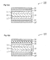
- FIG. 1(a) is a schematic sectional view of a liquid crystal panel according to an embodiment of the present invention.
- a liquid crystal panel 100 is provided with: a liquid crystal cell 10; a first polarizer 20 arranged on one side (on a viewer side in the figure) of the liquid crystal cell 10; a second polarizer 20' arranged on another side (on a backlight side in the figure) of the liquid crystal cell 10 ; and at least two optical compensation layers arranged between the first polarizer 20 and the second polarizer 20'.
- At least two compensation layers include a first optical compensation layer 30 and a second optical compensation layer 40.
- the first optical compensation layer 30 is arranged between the first polarizer 20 and the liquid crystal cell 10
- the second optical compensation layer 40 is arranged between the second polarizer 20' and the liquid crystal cell 10.
- the first compensation layer 30 may serve as a protective layer on a liquid crystal cell side of the first polarizer
- the second optical compensation layer 40 may serve as a protective layer on a liquid crystal side of the second polarizer 20'.
- this embodiment may contribute to reduction in thickness of a liquid crystal panel (eventually, a liquid crystal display apparatus).
- Fig. 1(b) is a schematic sectional view of a liquid crystal panel according to another embodiment of the present invention.
- a protective layer 50 is provided between the first polarizer 20 and the first optical compensation layer 30.
- the protective layer 50 is arranged adjacent to the liquid crystal cell side of the first polarizer 20, and the first optical compensation layer 30 is arranged adjacent to the liquid crystal cell side of the protective layer 50.
- the protective layer 50 is provided, to thereby significantly prevent degradation of the polarizer and provide a liquid crystal panel having excellent durability.
- the first optical compensation layer 30 may be arranged on the backlight side and the second optical compensation layer 40 may be arranged on the viewer side, but the first optical compensation layer 30 is preferably arranged on the viewer side as shown in the figure. This is because effects of heat of backlight can be reduced, to thereby exert effects of the present invention.
- any appropriate protective layer may be provided between the second polarizer 20' and the second optical compensation layer 40.
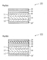
- Fig. 2(a) is a schematic sectional view of a liquid crystal panel according to still another embodiment of the present invention.
- the first optical compensation layer 30 and the second optical compensation layer 40 are arranged between the first polarizer 20 and the liquid crystal cell 10.
- the first optical compensation layer 30 may serve as a protective layer on the liquid crystal cell side of the first polarizer 20.
- this embodiment may contribute to reduction in thickness of a liquid crystal panel (eventually, a liquid crystal display apparatus).
- Fig. 2(b) is a schematic sectional view of a liquid crystal panel according to yet another embodiment of the present invention.
- the protective layer 50 is provided between the first polarizer 20 and the first optical compensation layer 30.
- the protective layer 50 is arranged adjacent to the liquid crystal cell side of the first polarizer 20, and the first optical compensation layer 30 is arranged adjacent to the liquid crystal cell side of the protective layer 50.
- the protective layer 50 is provided, to thereby significantly prevent degradation of the polarizer and provide a liquid crystal panel having excellent durability. Note that positions of the first optical compensation layer 30 and the second optical compensation layer 40 may be reversed.
- the first optical compensation layer 30 and the second optical compensation layer 40 are preferably arranged on different sides of the liquid crystal cell 10. This is because a product can be designed without considering a method of laminating the first optical compensation layer 30 and the second optical compensation layer 40, and this arrangement provides excellent productivity.
- any appropriate protective layer may be provided between the first polarizer 20 or the second polarizer 20', and the second optical compensation layer 40 as required. Further, any appropriate protective layer may be provided on a side without an optical compensation layer of the first polarizer 20 and/or the second polarizer 20' as required. The protective layer is provided, to thereby prevent degradation of the polarizers. In the present invention, another optical compensation layer (not shown) may be provided. The kind, number, position, and the like of such an optical compensation layer may appropriately be selected in accordance with the purpose. In the liquid crystal panel of the present invention, the respective layers (films) are laminated through any appropriate pressure-sensitive adhesive layer or adhesive layer.
- the liquid crystal cell 10 includes: a pair of substrates 11 and 11' ; and a liquid crystal layer 12 as a display medium arranged between the substrates 11 and 11' .
- a color filter and a black matrix are provided on one substrate 11 (color filter substrate).
- a switching element (typically TFT, not shown) for controlling electrooptic properties of liquid crystals, a scanning line (not shown) for providing a gate signal to the switching element, a signal line (not shown) for providing a source signal to the switching element, and a pixel electrode and a counter electrode (both not shown) are provided on the other substrate (active matrix substrate) 11'.
- the color filter may be provided on an active matrix substrate 11' side.
- a distance (cell gap) between the substrates 11 and 11' is controlled by a spacer (not shown).
- any appropriate drive mode can be employed for drive mode of the liquid crystal cell 10 as long as effects of the present invention can be obtained.
- the drive mode include STN (Super Twisted Nematic) mode, TN (Twisted Nematic) mode, IPS (In-Plane Switching) mode, VA (Vertical Aligned) mode, OCB (Optically AlignedBirefringence)mode,HAN(Hybrid Aligned Nematic) mode, and ASM (Axially Symmetric Aligned Microcell) mode.
- STN Super Twisted Nematic
- TN Transmission Nematic
- IPS In-Plane Switching
- VA Very Aligned
- OCB Optically AlignedBirefringence
- ASM Analy Symmetric Aligned Microcell
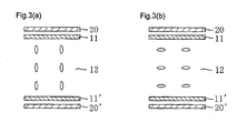
- Figs. 3(a) and 3(b) are each a schematic sectional view explaining an alignment state of liquid crystal molecules in VA mode.
- the liquid crystal molecules are aligned vertically to surfaces of the substrates 11 and 11' under no voltage application.
- Such vertical alignment may be realized by arranging nematic liquid crystals having negative dielectric anisotropy between substrates each having formed thereon a vertically aligned film (not shown).
- No birefringence generates in a long axis direction of the liquid crystal molecules such that incident light advances without changing a polarization direction and is absorbed by the second polarizer 20' having a polarization axis perpendicular to the first polarizer 20. In this way, dark display is obtained under no voltage application (normallyblackmode).
- long axes of the liquid crystal molecules align parallel to the surfaces of the substrates under voltage application between electrodes.
- the liquid crystal molecules exhibit birefringence with respect to linear polarized light entering the liquid crystal layer 12 in such a state, and a polarization state of incident light varies depending on inclination of the liquid crystal molecules.
- Figs. 4(a) to 4(d) are each a schematic sectional view explaining an alignment state of liquid crystal molecules in OCB mode.
- the OCB mode refers to drive mode in which the liquid crystal layer 12 is formed of so-called bend alignment.
- the bend alignment refers to an alignment state in which: nematic liquid crystal molecules are aligned at a substantially parallel angle (alignment angle) in a vicinity of a substrate; the alignment angle forms a vertical angle with respect to a plane of the substrate toward the center of the liquid crystal layer; the alignment changes progressively and continuously to be parallel to the opposing substrate surface away from the center of the liquid crystal layer; and no twisted structure exists throughout the liquid crystal layer.
- Such bend alignment is formed as described below.
- the liquid crystal molecules have substantially homogenous alignment in a state in the absence of an electric field (initial state). However, the liquid crystal molecules each have a pretilt angle, and a pretilt angle in the vicinity of the substrate differs from a pretilt angle in the vicinity of the opposing substrate.
- a predetermined bias voltage typically, 1.5 V to 1.9 V
- the liquid crystal molecules undergo a spray alignment as shown in Fig. 4(b) and transfer to a bend alignment as shown in Fig. 4(c).
- the liquid crystal molecules in a bend alignment state align substantially vertically to the surface of the substrate as shown in Fig. 4(d) .
- a display voltage typically, 5 V to 7 V
- the liquid crystal molecules in a bend alignment state align substantially vertically to the surface of the substrate as shown in Fig. 4(d) .
- light allowed to pass through the first polarizer 20 and to enter the liquid crystal layer in a state as shown in Fig. 4(d) under high voltage application advances without changing a polarization direction and is absorbed by the second polarizer 20' , to thereby provide dark display.
- Reduction in display voltage returns the liquid crystal molecules into bend alignment by alignment control force of rubbing treatment, to thereby provide light display again.
- the inclination of the liquid crystal molecules is controlled by varying a display voltage.
- a liquid crystal display apparatus provided with a liquid crystal cell of OCB mode allows very high speed switching of phase transfer from spray alignment state to bend alignment state, and thus has a characteristic of better movie display properties than those of a liquid crystal display apparatus provided with a liquid crystal cell of other drive mode such as TN mode or IPS mode.
- the liquid crystal panel as described above may suitably be used for a liquid crystal display apparatus such as a personal computer, a liquid crystal television, a cellular phone, a portable digital assistance (PDA), or a projector.
- a liquid crystal display apparatus such as a personal computer, a liquid crystal television, a cellular phone, a portable digital assistance (PDA), or a projector.
- PDA portable digital assistance
- the "polarizing plate” refers to an optical element arranged on each side of a liquid crystal cell and including a polarizer.
- the polarizing plate may employ any appropriate structure as long as the polarizing plate is an optical element including a polarizer.
- Typical examples of the polarizing plate include: a polarizing plate having a structure of "protective layer/polarizer/protective layer”; a polarizing plate having a structure of "protective layer/polarizer/protective layer/optical compensation layer”; a polarizing plate having a structure of "protective layer/polarizer/protective layer/optical compensation layer/optical compensation layer”; a polarizing plate having a structure of "protective layer/polarizer/optical compensation layer”; and a polarizing plate having a structure of "protective layer/polarizer/optical compensation layer/optical compensation layer”.
- Typical examples of the optical compensation layer include the first optical compensation layer, the second optical compensation layer, and the other optical compensation layer described in the above section A.
- the first polarizing plate is arranged on one side of the liquid crystal cell, and the second polarizing plate is arranged on another side of the liquid crystal cell.
- the structures of the first polarizing plate and the structure of the second polarizing plate may be identical to or different from each other.
- the first polarizing plate includes a first waterproof part on at least a part of its side surface
- the second polarizing plate includes a second waterproof part on at least a part of its side surface.
- the "side surface" of the polarizing plate refers to an end surface of the polarizing plate in a thickness direction.
- the first polarizing plate preferably has a substantially rectangular shape.
- the first waterproof part preferably includes four corners of the first polarizing plate.
- the first waterproof part includes the four corners of the first polarizing plate, to thereby completely provide a display without uneven brightness across an entire panel surface of a liquid crystal panel to be obtained.
- the first waterproof part is provided for preferably 1/10 or more, more preferably 1/4 or more, furthermore preferably 1/2 or more, particularly preferably 3/4 of the side surface, and most preferably the entire side surface of the first polarizing plate.
- the waterproof part is provided to an area as large as possible of the side surface of the first polarizing plate, to thereby further completely provide a display without uneven brightness across an entire panel surface of a liquid crystal panel to be obtained.
- the second polarizing plate preferably has a substantially rectangular shape.
- the second waterproof part preferably includes four corners of the second polarizing plate.
- the second waterproof part includes the four corners of the second polarizing plate, to thereby completely provide a display without uneven brightness across an entire panel surface of a liquid crystal panel to be obtained.
- the second waterproof part is provided for preferably 1/10 or more, more preferably 1/4 or more, furthermore preferably 1/2 or more, particularly preferably 3/4 of the side surface, and most preferably the entire side surface of the second polarizing plate.
- the waterproof part is provided to an area as large as possible of the side surface of the second polarizing plate, to thereby further completely provide a display without uneven brightness across an entire panel surface of a liquid crystal panel to be obtained.
- the first waterproof part and the second waterproof part each have a water contact angle of preferably 80° or more, and more preferably 100° or more.
- a water contact angle of 80° or more can develop sufficient water repellent property.
- the first waterproof part and the second waterproof part can be provided by employing any appropriate waterproof method.
- a waterproof part can be provided by applying a waterproof agent by spraying or the like on the side surface of the first polarizing plate or the second polarizing plate.
- the waterproof agent may employ any appropriate waterproof agent.
- a releasing agent may be used as the waterproof agent.
- the releasing agent include: a silicone-based releasing agent such as dimethyl silicone oil, dimethyl silicone rubber, a silicone resin, or an organic modified silicone resin; a fatty ester-based releasing agent such as ethylene glycol fatty ester, sorbitol fatty ester, or polyoxyethylene fatty ester; a phosphate ester-based releasing agent such as polyoxyalkylene phosphate ester; an alcohol-based releasing agent such as polyoxyalkylene glycol, glycols, or polyoxyethylene higher alcohol ether; and fluorine-based releasing agent such as a fluorine resin including polytetrafluoroethylene or a tetrafluoroethylene/perfluoroalkyl vinyl ether copolymer, vinylidene fluoride, fluorine rubber such as hexafluoropropylene-based rubber, a fluorine-based surfactant, flu
- any appropriate optical compensation layer may be employed without inhibiting the purpose of the present invention.
- the first optical compensation layer may employ any appropriate optical compensation layer as described above.
- a typical specific example thereof is an optical compensationlayer having the following properties.
- the first optical compensation layer has an absolute value of photoelastic coefficient of preferably 40 ⁇ 10 -12 m 2 /N or less, more preferably 0.2 ⁇ 10 -12 to 35 ⁇ 10 -12 m 2 /N, and furthermore preferably 0.2 ⁇ 10 -12 to 30 ⁇ 10 -12 m 2 /N.
- the absolute value of photoelastic coefficient is adjusted within the above ranges, to thereby effectively suppress display unevenness.
- the first optical compensation layer preferably has a refractive index profile of nx > ny ⁇ nz. Further, the first optical compensation layer preferably has so-called reverse wavelength dispersion property. Specifically, in-plane retardations preferably have a relationship of ⁇ nd(380) ⁇ And(550) ⁇ ⁇ nd(780). More preferably, the in-plane retardations preferably have a relationship of And(780)/And(550) > 1.10. Such relationships can realize favorable optical compensation throughout a wide region of visible light.
- a lower limit of the in-plane retardation ⁇ nd(550) of the first optical compensation layer is preferably 90 nm or more, more preferably 120 nm or more, and furthermore preferably 130 nm or more.
- an upper limit of ⁇ nd(550) is preferably 200 nm or less, more preferably 170 nm or less, and furthermore preferably 160 nm or less.
- a lower limit of the in-plane retardation And(550) of the first optical compensation layer is preferably 50 nm or more, more preferably 70 nm or more, and furthermore preferably 75 nm or more.
- an upper limit of ⁇ nd(550) is preferably 150 nm or less, more preferably 110 nm or less, and furthermore preferably 100 nm or less.
- the thickness of the first optical compensation layer may employ any appropriate thickness as long as the effects of the present invention can be provided. Specifically, the thickness is preferably 20 to 160 ⁇ m, more preferably 40 to 140 ⁇ m, and furthermore preferably 60 to 120 ⁇ m.
- the first optical compensation layer may typically be formed through stretching treatment of a polymer film.
- the kind, stretching conditions, stretching method, and the like of the polymer are appropriately selected, to thereby provide a first optical compensation layer having optical properties (refractive index profile, in-plane retardations, and photoelastic coefficient) described above.
- a material to be included in the polymer film may employ any appropriate material, but the polymer film preferably contains a cellulose-based material.
- the cellulose-based material is preferably substituted by an acetyl group and a propionyl group.
- a lower limit of a degree of substitution of the cellulose-based material “DSac (degree of acetyl substitution) + DSpr (degree of propionyl substitution) " (indicating how many of three hydroxyl groups present in a repeating unit of cellulose is substituted by an acetyl group or a propionyl group on average) is preferably 2 or more, more preferably 2.3 or more, and furthermore preferably 2.6 or more.
- An upper limit of "DSac + DSpr” is preferably 3 or less, more preferably 2.9 or less, and furthermore preferably 2.8 or less.
- the degree of substitution of the cellulose-based material is adjusted within the above ranges, to thereby provide an optical compensation layer having a desired refractive index profile as described above.
- a lower limit of DSpr (degree of propionyl substitution) is preferably 1 or more, more preferably 2 or more, and furthermore preferably 2.5 or more.
- An upper limit of DSpr is preferably 3 or less, more preferably 2.9 or less, and furthermore preferably 2.8 or less.
- DSpr is adjusted within the above ranges, to thereby improve solubility of the cellulose-based material in a solvent and facilitate control of the thickness of the first optical compensation layer to be obtained. Further, "DSac + DSpr" is adjusted within the above ranges and DSpr is adjusted within the above ranges, to thereby provide an optical compensation layer having the optical properties described above and having reverse wavelength dispersion property.
- DSac degree of acetyl substitution
- DSpr degree of propionyl substitution
- the cellulose-based material may have a substituent excluding the acetyl group and the propionyl group.
- substituents include: an ester group such as a butyrate group; and an ether group such as an alkyl ether group or an aralkylene ether group.
- a number average molecular weight of the cellulose-based material is preferably 5, 000 to 100, 000, and more preferably 10, 000 to 70, 000. The number average molecular weight thereof is adjusted within the above ranges, to thereby provide excellent productivity and favorable mechanical strength.
- a method of substituting the acetyl group and propionyl group may employ any appropriate method.
- cellulose may be treated with a strong caustic soda solution to prepare alkali cellulose, and alkali cellulose and a predetermined amount of a mixture of acetic anhydride and propionic anhydride are mixed for acylation.
- An acyl group is partly hydrolyzed for adjusting the degree of substitution "DSac + DSpr".
- the polymer film may contain any appropriate polymer material.
- the polymer material include: a cellulose ester such as cellulose butyrate; and a cellulose ether such as methyl cellulose or ethyl cellulose.
- the polymer film may contain additives such as a plasticizer, a heat stabilizer, and a UV stabilizer as required.
- the second optical compensation layer may employ any appropriate optical compensation layer.
- Atypical specific example thereof is an optical compensation layer having the following properties.
- a lower limit of the thickness direction retardation Rth (550) of the second optical compensation layer is preferably 10 nm or more, more preferably 20 nm or more, and furthermore preferably 50 nm or more. Meanwhile, an upper limit of the thickness direction retardation Rth(550) is preferably 1, 000 nm or less, more preferably 500 nm or less, and furthermore preferably 250 nm or less.
- the second optical compensation layer may be a monolayer or a laminate of two or more layers.
- the material used for forming each layer and the thickness of each layer may appropriately be set as long as the laminate as a whole has optical properties as described above.
- the thickness of the second optical compensation layer may employ any appropriate thickness as long as the effects of the present invention can be provided. Specifically, the thickness is preferably 0.1 to 50 ⁇ m, more preferably 0.5 to 30 ⁇ m, and furthermore preferably 1 to 10 ⁇ m.
- a material used for forming the second optical compensation layer may employ any appropriate material as long as the optical properties as described above can be obtained.
- An example of the material is a non-liquid crystalline material.
- a particularly preferred example thereof is a non-liquid crystalline polymer.
- a step of applying an aligned film to its surface, laminating an aligned film thereon, or the like may be omitted.
- a preferred example of the non-liquid crystalline material includes a polymer such as polyamide, polyimide, polyester, polyetherketone, polyamideimide, or polyesterimide since such a material has excellent thermal resistance, excellent chemical resistance, excellent transparency, and sufficient rigidity.
- a polymer such as polyamide, polyimide, polyester, polyetherketone, polyamideimide, or polyesterimide since such a material has excellent thermal resistance, excellent chemical resistance, excellent transparency, and sufficient rigidity.
- One type of polymer may be used, or a mixture of two or more types thereof having different functional groups such as a mixture of polyaryletherketone and polyamide may be used.
- polyimide is particularly preferred in view of high transparency, high alignment ability, and high extension.
- a molecular weight of the polymer is not particularly limited.
- the polymer has a weight average molecular weight (Mw) of preferably within a range of 1, 000 to 1, 000, 000, more preferably within a range of 2,000 to 500,000, for example.
- Polyimide which has high in-plane alignment ability and which is soluble in an organic solvent is preferred as polyimide used in the present invention, for example. More specifically, a polymer disclosed in JP 2000-511296 A , containing a condensation polymerization product of 9, 9-bis (aminoaryl) fluorene and aromatic tetracarboxylic dianhydride, and containing at least one repeating unit represented by the following formula (1) can be used.
- R 3 to R 6 independently represent at least one type of substituent selected from hydrogen, a halogen, a phenyl group, a phenyl group substituted with 1 to 4 halogen atoms or 1 to 4 alkyl groups each having 1 to 10 carbon atoms, and an alkyl group having 1 to 10 carbon atoms.
- R 3 to R 6 independently represent at least one type of substituent selected from a halogen, a phenyl group, a phenyl group substituted with 1 to 4 halogen atoms or 1 to 4 alkyl groups each having 1 to 10 carbon atoms, and an alkyl group having 1 to 10 carbon atoms.
- Z represents a tetravalent aromatic group having 6 to 20 carbon atoms, and preferably represents a pyromellitic group, a polycyclic aromatic group, a derivative of the polycyclic aromatic group, or a group represented by the following formula (2), for example.
- Z' represents a covalent bond, a C(R 7 ) 2 group, a CO group, an O atom, an S atom, an SO 2 group, an Si (C 2 H 5 ) 2 group, or an NR 8 group.
- a plurality of Z' s may be the same or different from each other.
- w represents an integer of 1 to 10.
- R 7 s independently represent hydrogen or a C(R 9 ) 3 group.
- R 8 represents hydrogen, an alkyl group having 1 to about 20 carbon atoms, or an aryl group having 6 to 20 carbon atoms.
- a plurality of R 8 s may be the same or different from each other.
- R 9 s independently represent hydrogen, fluorine, or chlorine.
- polycyclic aromatic group includes a tetravalent group derived fromnaphthalene, fluorene, benzofluorene, or anthracene.
- substituted derivative of the polycyclic aromatic group includes the above polycyclic aromatic group substituted with at least a group selected from an alkyl group having 1 to 10 carbon atoms, a fluorinated derivative thereof, and a halogen such as F or Cl.
- polyimide represented by the following formula (5) is a preferred form of the homopolymer represented by the following formula (3).
- G and G' independently represent a covalent bond, a CH 2 group, a C(CH 3 ) 2 group, a C(CF 3 ) 2 group, a C (CX 3 ) 2 group (wherein, X represents a halogen), a CO group, an O atom, an S atom, an SO 2 group, an Si (CH 2 CH 3 ) 2 group, or an N (CH 3 ) group, for example.
- G and G' may be the same or different from each other.
- L is a substituent, and d and e each represent the number of the substituents.
- L represents a halogen, an alkyl group having 1 to 3 carbon atoms, a halogenated alkyl group having 1 to 3 carbon atoms, a phenyl group, or a substituted phenyl group, for example.
- a plurality of Ls may be the same or different from each other.
- An example of the substituted phenyl group includes a substituted phenyl group having at least one type of substituent selected from a halogen, an alkyl group having 1 to 3 carbon atoms, and a halogenated alkyl group having 1 to 3 carbon atoms, for example.
- the halogen include fluorine, chlorine, bromine, and iodine.
- d represents an integer of 0 to 2
- e represents an integer of 0 to 3.
- Q is a substituent, and f represents the number of the substituents.
- Q represents an atom or a group selected from hydrogen, a halogen, an alkyl group, a substituted alkyl group, a nitro group, a cyano group, a thioalkyl group, an alkoxy group, an aryl group, a substituted aryl group, an alkyl ester group, and a substituted alkyl ester group, for example .
- a plurality of Qs may be the same or different from each other.
- the halogen include fluorine, chlorine, bromine, and iodine.
- An example of the substituted alkyl group includes a halogenated alkyl group.
- An example of the substituted aryl group includes a halogenated aryl group.
- f represents an integer of 0 to 4
- g represents an integer of 0 to 3.
- h represents an integer of 1 to 3.
- g and h are each preferably larger than 1.
- R 10 and R 11 independently represent an atom or a group selected from hydrogen, a halogen, a phenyl group, a substituted phenyl group, an alkyl group, and a substituted alkyl group.
- R 10 and R 11 independently represent a halogenated alkyl group.
- M 1 and M 2 independently represent a halogen, an alkyl group having 1 to 3 carbon atoms, a halogenated alkyl group having 1 to 3 carbon atoms, a phenyl group, or a substituted phenyl group, for example.
- the halogen include fluorine, chlorine, bromine, and iodine.
- An example of the substituted phenyl group includes a substituted phenyl group having at least one type of substituent selected from the group consisting of a halogen, an alkyl group having 1 to 3 carbon atoms, and a halogenated alkyl group having 1 to 3 carbon atoms.
- a specific example of the polyimide represented by the above formula (3) includes a compound represented by the following formula (6)
- polyimide includes a copolymer prepared through arbitrary copolymerization of acid dianhydride having a skeleton (repeating unit) other than that as described above and diamine.
- An example of the acid dianhydride includes an aromatic tetracarboxylic dianhydride.
- aromatic tetracarboxylic dianhydride examples include pyromellitic dianhydride, benzophenone tetracarboxylic dianhydride, naphthalene tetracarboxylic dianhydride, heterocyclic aromatic tetracarboxylic dianhydride, and 2,2'-substituted biphenyltetracarboxylic dianhydride.
- pyromellitic dianhydride examples include: pyromellitic dianhydride; 3,6-diphenyl pyromellitic dianhydride; 3,6-bis(trifluoromethyl)pyromellitic dianhydride; 3, 6-dibromopyromellitic dianhydride;and3,6-dichloropyromellitic dianhydride.
- benzophenone tetracarboxylic dianhydride examples include: 3,3',4,4'-benzophenone tetracarboxylic dianhydride; 2,3,3',4'-benzophenone tetracarboxylic dianhydride; and 2,2',3,3'-benzophenone tetracarboxylic dianhydride.
- naphthalene tetracarboxylic dianhydride examples include: 2,3,6,7-naphthalene tetracarboxylic dianhydride; 1,2,5,6-naphthalene tetracarboxylic dianhydride; and 2,6-dichloronaphthalene-1,4,5,8-tetracarboxylic dianhydride.
- heterocyclic aromatic tetracarboxylic dianhydride include: thiophene-2,3,4,5-tetracarboxylic dianhydride; pyrazine-2,3,5,6-tetracarboxylic dianhydride; and pyridine-2,3,5,6-tetracarboxylic dianhydride.
- Examples of the 2,2'-substituted biphenyltetracarboxylic dianhydride include: 2,2'-dibromo-4,4',5,5'-biphenyltetracarboxylic dianhydride; 2,2' -dichloro-4, 4 ' , 5, 5 ' -biphenyltetracarboxylic dianhydride; and 2,2'-bis(trifluoromethyl)-4,4',5,5'-biphenyltetracarboxylic dianhydride.
- aromatic tetracarboxylic dianhydride examples include: 3,3',4,4'-biphenyltetracarboxylic dianhydride; bis(2,3-dicarboxyphenyl)methane dianhydride; bis(2,5,6-trifluoro-3,4-dicarboxyphenyl)methane dianhydride; 2,2-bis(3,4-dicarboxyphenyl)-1,1,1,3,3,3-hexafluoropropane dianhydride; 4,4'-bis(3,4-dicarboxyphenyl)-2,2-diphenylpropane dianhydride; bis(3,4-dicarboxyphenyl)ether dianhydride; 4,4'-oxydiphthalic dianhydride; bis(3,4-dicarboxyphenyl)sulfonic dianhydride; 3,3',4,4'-diphenylsulfone tetracarboxylic dianhydride; 4,4'-[4,4]
- the aromatic tetracarboxylic dianhydride is preferably 2,2'-substituted biphenyltetracarboxylic dianhydride, more preferably 2,2'-bis(trihalomethyl)-4,4',5,5'-biphenyltetracarboxylic dianhydride, and furthermore preferably 2,2'-bis(trifluoromethyl)-4,4',5,5'-biphenyltetracarboxylic dianhydride.
- diamine includes aromatic diamine.
- aromatic diamine include benzenediamine, diaminobenzophenone, naphthalenediamine, heterocyclic aromatic diamine, and other aromatic diamines.
- Examples of the benzenediamine include benzenediamines such as o-, m-, or p-phenylenediamine, 2,4-diaminotoluene, 1,4-diamino-2-methoxybenzene, 1,4-diamino-2-phenylbenzene, and 1, 3-diamino-4-chlorobenzene.
- Examples of the diaminobenzophenone include 2,2'-diaminobenzophenone and 3,3'-diaminobenzophenone.
- Examples of the naphthalenediamine include 1, 8-diaminonaphthalene and 1, 5-diaminonaphthalene.
- Examples of the heterocyclic aromatic diamine include 2,6-diaminopyridine, 2,4-diaminopyridine, and 2,4-diamino-S-triazine.
- aromatic diamine examples include: 4,4'-diaminobiphenyl; 4,4'-diaminodiphenylmethane; 4,4'-(9-fluorenylidene)-dianiline; 2,2'-bis(trifluoromethyl)-4,4'-diaminobiphenyl; 3,3'-dichloro-4,4'-diaminodiphenylmethane; 2,2'-dichloro-4,4'-diaminobiphenyl; 2,2',5,5'-tetrachlorobenzidine; 2,2-bis(4-aminophenoxyphenyl)propane; 2,2-bis(4-aminophenyl)propane; 2,2-bis(4-aminophenyl)-1,1,1,3,3,3-hexafluoropropane; 4,4'-diaminodiphenyl ether; 3,4'-diaminodiphenyl ether; 1,3-bis(3-bis
- polyetherketone includes polyaryletherketone disclosed in JP 2001-049110 A and represented by the following general formula (7).
- X represents a substituent
- q represents the number of the substituents.
- X represents a halogen atom, a lower alkyl group, a halogenated alkyl group, a lower alkoxy group, or a halogenated alkoxy group, for example.
- a plurality of Xs may be the same or different from each other.
- halogen atom examples include a fluorine atom, a bromine atom, a chlorine atom, and an iodine atom. Of those, a fluorine atom is preferred.
- the lower alkyl group is preferably an alkyl group having a straight chain or branched chain of 1 to 6 carbon atoms, more preferably an alkyl group having a straight chain or branched chain of 1 to 4 carbon atoms.
- the lower alkyl group is preferably a methyl group, an ethyl group, a propyl group, an isopropyl group, a butyl group, an isobutyl group, a sec-butyl group, or a tert-butyl group, and particularly preferably a methyl group or an ethyl group.
- An example of the halogenated alkyl group includes a halide of the above lower alkyl group such as a trifluoromethyl group.
- the lower alkoxy group is preferably an alkoxy group having a straight chain or branched chain of 1 to 6 carbon atoms, more preferably an alkoxy group having a straight chain or branched chain of 1 to 4 carbon atoms.
- the lower alkoxy group is preferably a methoxy group, an ethoxy group, a propoxy group, an isopropoxy group, a butoxy group, an isobutoxy group, a sec-butoxy group, or a tert-butoxy group, and particularly preferably a methoxy group or an ethoxy group.
- An example of the halogenated alkoxy group includes a halide of the above lower alkoxy group such as a trifluoromethoxy group.
- q is an integer of 0 to 4.
- q 0, and a carbonyl group and an oxygen atom of ether bonded to both ends of a benzene ring are located in para positions.
- R 1 is a group represented by the following formula (8), and m is an integer of 0 or 1.
- X' represents a substituent which is the same as X in the above formula (7), for example.
- a plurality of X's may be the same or different from each other.
- q' represents the number of the substituents X'.
- q' is an integer of 0 to 4, and q' is preferably 0.
- p is an integer of 0 or 1.
- R 2 represents a divalent aromatic group.
- the divalent aromatic group include: an o-, m-, or p-phenylene group; and a divalent group derived from naphthalene, biphenyl, anthracene, o-, m-, or p-terphenyl, phenanthrene, dibenzofuran, biphenyl ether, or biphenyl sulfone.
- hydrogen directly bonded to an aromatic group may be substituted with a halogen atom, a lower alkyl group, or a lower alkoxy group.
- R 2 is preferably an aromatic group selected from groups represented by the following formulae (9) to (15).
- R 1 is preferably a group represented by the following formula (16) .
- R 2 and p are defined as those in the above formula (8).
- n represents a degree of polymerization. n falls within a range of 2 to 5,000, preferably within a range of 5 to 500, for example.
- Polymerization may involve polymerization of repeating units of the same structure or polymerization of repeating units of different structures. In the latter case, a polymerization form of the repeating units may be block polymerization or random polymerization.
- Terminals of the polyaryletherketone represented by the above formula (7) are preferably a fluorine atom on a p-tetrafluorobenzoylene group side and a hydrogen atom on an oxyalkylene group side.
- Such polyaryletherketone can be represented by the following general formula (17), for example.
- n represents the same degree of polymerization as that in the above formula (7).
- polyaryletherketone represented by the above formula (7) examples include compounds represented by the following formulae (18) to (21). In each of the following formulae, n represents the same degree of polymerization as that in the above formula (7).
- polyamide or polyester includes polyamide or polyester disclosed in JP 10-508048 A .
- a repeating unit thereof can be represented by the following general formula (22), for example.
- Y represents O or NH.
- E represents at least one selected from a covalent bond, an alkylene group having 2 carbon atoms, a halogenated alkylene group having 2 carbon atoms, a CH 2 group, a C(CX 3 ) 2 group (wherein, X is a halogen or hydrogen), a CO group, an O atom, an S atom, an SO 2 group, an Si(R) 2 group, and an N (R) group, for example.
- a plurality of Es may be the same or different from each other.
- R is at least one of an alkyl group having 1 to 3 carbon atoms and a halogenated alkyl group having 1 to 3 carbon atoms, and is located in a meta or para position with respect to a carbonyl functional group or a Y group.
- a and A' each represent a substituent, and t and z represent the numbers of the respective substituents.
- p represents an integer of 0 to 3
- q represents an integer of 1 to 3.
- r represents an integer of 0 to 3.
- A is selected from hydrogen, a halogen, an alkyl group having 1 to 3 carbon atoms, a halogenated alkyl group having 1 to 3 carbon atoms, an alkoxy group represented by OR (wherein, R is defined as above), an aryl group, a substituted aryl group prepared through halogenation or the like, an alkoxycarbonyl group having 1 to 9 carbon atoms, an alkylcarbonyloxy group having 1 to 9 carbon atoms, an aryloxycarbonyl group having 1 to 12 carbon atoms, an arylcarbonyloxy group having 1 to 12 carbon atoms and its substituted derivatives, an arylcarbamoyl group having 1 to 12 carbon atoms, and arylcarbonylamino group having 1 to 12 carbon atoms and its substituted derivatives, for example.
- a plurality of As may be the same or different from each other.
- A' is selected from a halogen, an alkyl group having 1 to 3 carbon atoms, a halogenated alkyl group having 1 to 3 carbon atoms, a phenyl group, and a substituted phenyl group, for example.
- a plurality of A's may be the same or different from each other.
- Examples of the substituent on a phenyl ring of the substituted phenyl group include a halogen, an alkyl group having 1 to 3 carbon atoms, a halogenated alkyl group having 1 to 3 carbon atoms, and the combination thereof.
- t represents an integer of 0 to 4
- z represents an integer of 0 to 3.
- the repeating unit of the polyamide or polyester represented by the above formula (22) is preferably a repeating unit represented by the following general formula (23).
- A, A', and Y are defined as those in the above formula (22).
- v represents an integer of 0 to 3, preferably an integer of 0 to 2.
- x and y are each 0 or 1, but are not both 0.
- a solution of at least one polymer selected from the group consisting of polyamide, polyimide, polyester, polyetherketone, polyamideimide, and polyesterimide is applied to a transparent polymer film and is dried to form the polymer layer on the transparent polymer film. Then, the transparent polymer film and the polymer layer may be stretched or contracted integrally, to thereby obtain the second optical compensation layer.
- Examples of the solvent of the coating solution include, but not limited to: halogenated hydrocarbons such as chloroform, dichloromethane, carbon tetrachloride, dichloroethane, tetrachloroethane, trichloroethylene, tetrachloroethylene, chlorobenzene, and ortho-dichlorobenzene; phenols such as phenol and parachlorophenol; aromatic hydrocarbons such as benzene, toluene, xylene, methoxybenzene, and 1,2-dimethoxybenzene; ketone-based solvents such as acetone, methyl ethyl ketone, methyl isobutyl ketone, cyclohexanone, cyclopentanone, 2-pyrrolidone, and N-methyl-2-pyrrolidone; ester-based solvents such as ethyl acetate and butyl a
- methyl isobutyl ketone is preferred, because non-liquid crystal materials exhibits high solubility in the solvent and the solvent does not corrode the substrate.
- solvents can be used alone, or two or more of them can be used in combination.
- the application solution may have any appropriate concentration of the non-liquid crystalline polymer as long as the above-mentioned optical compensation layer can be obtained and the application solution may be applied.
- the solution contains preferably 5 to 50 parts by weight, and more preferably 10 to 40 parts by weight of the non-liquid crystalline polymer with respect to 100 parts by weight of the solvent.
- the solution having a concentration within the above ranges has a viscosity allowing easy application.
- the application solution may further contain various additives such as a stabilizer, a plasticizer, and metals as required.
- the application solution may further contain another different resin as required.
- another different resin include various general-purpose resins, engineering plastics, a thermoplastic resin, and a thermosetting resin. Such a resin is used in combination, to thereby allow formation of an optical compensation layer having appropriate mechanical strength or durability in accordance with the purpose.
- Examples of the general-purpose resin include polyethylene (PE), polypropylene (PP), polystyrene (PS),polymethylmethacrylate (PMMA), an ABS resin, and an AS resin.
- Examples of the engineering plastic include polyacetate (POM), polycarbonate (PC), polyamide (PA: nylon), polyethylene terephthalate (PET), and polybutylene terephthalate (PBT).
- Examples of the thermoplastic resin include polyphenylene sulfide (PPS), polyether sulfone (PES), polyketone (PK), polyimide (PI), polycyclohexane dimethanol terephthalate (PCT), polyallylate (PAR), and a liquid crystal polymer (LCP).
- Examples of the thermosetting resin include an epoxy resin and a phenol novolac resin.
- the type and amount of another different resin to be added to the application solution may appropriately be set in accordance with the purpose.
- such a resin is added to the non-liquid crystalline polymer in a ratio of preferably 0 to 50 mass%, and more preferably 0 to 30 mass%.
- Examples of a method of applying the solution include: a spin coating method; a roll coating method; a flow coating method; a printing method; a dip coating method; a flow casting method; a bar coating method; and a gravure printing method.
- a polymer layer superposition method may also be used as required.
- the solvent in the above-mentioned solution is evaporated and removed by drying such as natural drying, air drying, or heat drying (at 60 to 250°C, for example), to thereby form a film-like optical compensation layer.
- the same film as that used for a protective layer to be described below may be used as the transparent polymer film.
- the second optical compensation layer may be used by peeling the first optical compensation layer off from the laminate (laminate having the first optical compensation layer formed on the transparent polymer film) obtained as described above, or used as the laminate itself.
- the transparent polymer film in the laminate may serve as a protective film of a polarizer to be described below.
- the first polarizing plate includes a first polarizer
- the second polarizer includes a second polarizer.
- Any appropriate polarizer may be employed as the first polarizer and the second polarizer used in the present invention depending on the purpose. Examples thereof include: a film prepared by adsorbing a dichromatic substance such as iodine or a dichromatic dye on a hydrophilic polymer film such as a polyvinyl alcohol-based film, a partially formalized polyvinyl alcohol-based film, or a partially saponified ethylene/vinyl acetate copolymer-based film and uniaxially stretching the film; and a polyene-based aligned film such as a dehydrated product of a polyvinyl alcohol-based film or a dehydrochlorinated product of a polyvinyl chloride-based film.
- a polarizer prepared by adsorbing a dichromatic substance such as iodine on a polyvinyl alcohol-based film and uniaxially stretching the film is particularly preferred because of its high polarized dichromaticity.
- a thickness of such a polarizer is generally, but not limited to, about 5 to 80 ⁇ m.
- the polarizer prepared by adsorbing iodine on a polyvinyl alcohol-based film and uniaxially stretching the film may be produced by, for example: immersing a polyvinyl alcohol-based film in an aqueous solution of iodine for coloring; and stretching the film to a 3 to 7 times length of the original length.
- the aqueous solution may contain boric acid, zinc sulfate, zinc chloride, or the like as required, or the polyvinyl alcohol-based film may be immersed in an aqueous solution of potassium iodide or the like. Further, the polyvinyl alcohol-based film may be immersed and washed in water before coloring as required.
- washing the polyvinyl alcohol-based film with water not only allows removal of contamination on a film surface or washing away of an antiblocking agent, but also provides an effect of preventing unevenness such as uneven coloring by swelling of the polyvinyl alcohol-based film.
- the stretching of the film may be performed after coloring of the film with iodine, performed during coloring of the film, or performed followed by coloring of the film with iodine.
- the stretching may be performed in an aqueous solution of boric acid, potassium iodide, or the like, or in a water bath.
- the protective layer is preferably transparent and colorless.
- the protective layer may employ any appropriate protective layer as long as it is capable of protecting a polarizer without inhibiting the effects of the present invention. Typical examples thereof include the following protective layers (1) to (3).
- the in-plane retardation ⁇ nd(550) of a protective layer (1) is preferably 0 nm or more and 10 nm or less, and more preferably 0 nm or more and 8 nm or less.
- the thickness direction retardation Rth(550) of the protective layer (1) is preferably 10 nm or more and 80 nm or less, more preferably 40 nm or more and 80 nm or less, and furthermore preferably 45 nm or more and 70 nm or less.
- the thickness of the protective layer (1) may appropriately be set in accordance with the purpose. Specifically, the thickness is preferably 20 to 140 ⁇ m, more preferably 40 to 120 ⁇ m, and furthermore preferably 60 to 100 ⁇ m.
- a material used for forming the protective layer (1) may employ any appropriate material.
- An example of the material is a plastic film having excellent transparency, mechanical strength, heat stability, moisture barrier properties, and the like.
- a resin used for forming the plastic film include an acetate resin such as triacetyl cellulose (TAC), a polyester resin, a polyether sulfone resin, a polysulfone resin, a polycarbonate resin, a polyamide resin, a polyimide resin, a polyolefin resin, an acrylic resin, a polynorbornene resin, a cellulose resin, a polyallylate resin, a polystyrene resin, a polyvinyl alcohol resin, a polyacrylic resin, and a mixture thereof.
- TAC triacetyl cellulose
- an acrylic, urethane-based, acryl urethane-based, epoxy-based, silicone-based, etc. heat-curable resin or UV-curable resin may also be used. From viewpoints of polarization properties and durability, a TAC film having a surface subj ected to saponification treatment with an alkali or the like is preferred.
- the in-plane retardation ⁇ nd(550) of a protective layer (2) is preferably 0 nm or more and 10 nm or less, more preferably 0 nm or more and 6 nm or less, and furthermore preferably 0 nm or more and 3 nm or less.
- the thickness direction retardation Rth (550) of the protective layer (2) is preferably 0 nm or more and 20 nm or less, more preferably 0 nm or more and 10 nm or less, furthermore preferably 0 nm or more and 6 nm or less, and particularly preferably 0 or more and 3 or less.
- the thickness of the protective layer (2) may appropriately be set in accordance with the purpose. Specifically, the thickness is preferably 20 to 200 ⁇ m, more preferably 30 to 100 ⁇ m, and furthermore preferably 35 to 95 ⁇ m.
- a cellulose-based film is typically used as the protective layer (2) .
- Acellulose-based filmhaving a large thickness direction retardation (Rth) is subjected to appropriate treatment for reducing the thickness direction retardation (Rth), to thereby favorably obtain the protective layer (2).
- the treatment for reducing the thickness direction retardation (Rth) may employ any appropriate treatment method. Examples thereof include: a method involving attaching a substrate formed of polyethylene terephthalate, polypropylene, stainless steel, or the like and having a solvent such as cyclopentanone or methyl ethyl ketone applied thereto together with a general cellulose-based film, drying the whole under heating (at about 80 to 150°C for about 3 to 10 minutes), and peeling off the substrate film; and a method involving applying a solution containing a norbornene-based resin, an acrylic resin, or the like dissolved in a solvent such as cyclopentanone or methyl ethyl ketone to a general cellulose-based film, drying the whole under heating (at about 80 to 150°C for about 3 to 10 minutes), and peeling off the applied film.
- a preferred example of a material used for forming the cellulose-based resin is a fatty acid-substituted cellulose-based polymer such as diacetyl cellulose or triacetyl cellulose.
- a fatty acid-substituted cellulose-based polymer such as diacetyl cellulose or triacetyl cellulose.
- triacetyl cellulose has a degree of acetic acid substitution of about 2.8.
- the degree of acetic acid substitution is preferably controlled to 1.8 to 2.7
- the degree of propionic acid substitution is more preferably controlled to 0.1 to 1, to thereby reduce the thickness direction retardation (Rth).
- a plasticizer such as dibutyl phthalate, p-toluenesulfonanilide, or acetyl triethyl citrate may be added to the aliphatic acid-substituted cellulose-based polymer, to thereby allow control of the thickness direction retardation (Rth) to a small value.
- An addition amount of the plasticizer is preferably 40 parts by weight or less, more preferably 1 to 20 parts by weight, and furthermore preferably 1 to 15 parts by weight with respect to 100 parts by weight of the aliphatic acid-substituted cellulose-based polymer.
- a preferred specific example of the protective layer (2) is an acrylic resin film.
- a preferred example of the acrylic resin film is an acrylic resin film containing as a main component an acrylic resin (A) having a glutaric anhydride unit represented by the following structural formula (24) and described in JP 2005-314534 A .
- the acrylic resin (A) having a glutaric anhydride unit represented by the following structural formula (1) may have improved heat resistance.
- R 1 and R 2 may be identical to or different from each other, and each represent a hydrogen atom or an alkyl group having 1 to 5 carbon atoms, more preferably a hydrogen atom or a methyl group, and furthermore preferably a methyl group.
- a ratio of the glutaric anhydride unit represented by the structural formula (24) is preferably 20 to 40 wt%, and more preferably 25 to 35 wt%.
- the acrylic resin (A) may contain one or two or more types of appropriate monomer units in addition to the glutaric anhydride unit represented by the structural formula (24).
- Apreferredexample of the monomer unit is a vinyl carboxylic acid alkyl ester unit.
- a ratio of the vinyl carboxylic acid alkyl ester unit is preferably 60 to 80 wt%, and more preferably 65 to 75 wt%.
- R 3 represents a hydrogen atom or an aliphatic or alicyclic hydrocarbon having 1 to 5 carbon atoms
- R 4 represents an aliphatic hydrocarbon having 1 to 5 carbon atoms.
- the acrylic resin (A) preferably has a weight average molecular weight of 80,000 to 150,000.
- a ratio of the acrylic resin (A) in the acrylic resin film is preferably 60 to 90 wt%.
- the acrylic resin film may contain one or two or more types of appropriate components in addition to the acrylic resin (A). Any appropriate component may be employed within a range not inhibiting the purpose of the present invention. Examples of the appropriate component include a resin except the acrylic resin (A), a UV absorber, an antioxidant, a lubricant, a plasticizer, a releasing agent, a color protection agent, a flame retardant, a nucleator, an antistatic agent, a pigment, and a colorant.
- a polymer film formed of a resin composition as described in JP 2001-343529 A may be used for the protective layer (3) .
- the resin composition refers to a mixture of: a thermoplastic resin having a substituted imide group or an unsubstituted imide group on a side chain; and a thermoplastic resin having a substituted phenyl group or an unsubstituted phenyl group, and a cyano group on a side chain.
- a specific example thereof is a resin composition containing: an alternating copolymer of isobutene and N-methylene maleimide; and an acrylonitrile/styrene copolymer. An extrusion molded product of such a resin composition may be used, for example.
- refractive indices nx, ny, and nz of a sample film were measured with a spectroscopic ellipsometer (M-220, manufactured by JASCO Corporation), and in-plane retardations And and thickness direction retardations Rth were calculated. Measurement wavelengths were 380 nm, 550 nm, and 780 nm.
- a photoelastic coefficient of the sample film was measured with a spectroscopic ellipsometer (M-220, manufactured by JASCO Corporation).
- a liquid was dropped on a substrate by using a solid-liquid interface analyzer ("Drop Master 300", trade name, manufactured by Kyowa Interface Science Co., Ltd.), and a contact angle after 5 seconds was measured. Measuring conditions were for static contact angle measurement. Ultrapure water was used as water, and a liquid drop was 0.5 ⁇ l. The measurement was repeated 10 times for each substrate, and an average value of the measurements was used as a measured value.
- Drop Master 300 trade name, manufactured by Kyowa Interface Science Co., Ltd.
- a brightness of a liquid crystal panel was measured by using a brightness measuring device ("CA-1500", trade name, manufactured by Konica Minolta Holdings, Inc.). Specifically, the measurement was conducted as described below. First, a liquid crystal panel was taken out of a liquid crystal display apparatus "BRAVIA 40-inch X-series" manufactured by Sony Corporation, and polarizing plates attached above and below a liquid crystal cell of the liquid crystal panel were peeled off. Then, polarizing plates produced in Examples or Comparative Examples were attached to both sides of the liquid crystal cell instead through an acrylicpressure-sensitive adhesive, to thereby produce a new liquid crystal panel.
- CA-1500 trade name, manufactured by Konica Minolta Holdings, Inc.
- the produced liquid crystal panel was re-installed in the liquid crystal display apparatus, and the resultant was left standing under conditions of 60°C and 95% RH for 250 hours. Then, the whole was left standing at room temperature for 3 hours, and left standing for 3 hours while backlight was turned on. Unevenness in brightness of the liquid crystal panel was evaluated at a measuring distance of 1 m. The evaluation of unevenness in brightness was conducted by measuring the brightness of a white part and a black display part. Measurement positions of the white part and the black display part were as described below.
- White part point inside liquid crystal panel at 1/30 length of long side and 1/30 length of short side from corner
- Black display part point at center of liquid crystal panel
- the obtained first optical compensation layer had a photoelastic coefficient of 25x10 -12 (m 2 /N) .
- the obtained first optical compensation layer had in-plane retardations ⁇ nd(380) of 65 nm, ⁇ nd(550) of 90 nm, andAnd(780) of 105 nm and thickness direction retardations Rth(380) of 69 nm, Rth(550) of 95 nm, and Rth(780) of 111 nm.
- the obtained first optical compensation layer had a refractive index profile of nx > ny ⁇ nz at 550 nm.
- the first optical compensation layer obtained as described above was attached to a polarizing plate (available from Nitto Denko Corporation, trade name: SEG1224) having a structure of TAC protective film (available from FUJIFILM Corporation, trade name: TF80UL) /polarizer/TAC protective film (trade name: TF80UL) through a pressure-sensitive adhesive (thickness of 20 ⁇ m), to thereby obtain a polarizing plate provided with a first optical compensation layer.
- a polarizing plate available from Nitto Denko Corporation, trade name: SEG12234
- TAC protective film available from FUJIFILM Corporation, trade name: TF80UL
- TF80UL polarizer/TAC protective film
- Polyimide synthesized from 2,2-bis(3,4-dicarboxyphenyl) hexafluoropropane dianhydride (6FDA) and 2,2'-bis(trifluoromethyl)-4,4'-diaminobiphenyl (TFMB) was dissolved in methyl isobutyl ketone (MIBK), to thereby prepare a 15 mass% polyimide solution.
- MIBK methyl isobutyl ketone
- This solution was applied to a triacetyl cellulose substrate (transparent polymer film) to a thickness of 30 ⁇ m. Then, the whole was subjected to drying treatment at 100°C for 10 minutes, to thereby obtain a second optical compensation layer having a thickness of about 4 ⁇ m.
- the obtained second optical compensation layer had in-plane retardations And(380) of 0.4 nm, ⁇ nd (550) of 0.3 nm, and ⁇ nd(780) of 0.3 nm and thickness direction retardations Rth(380) of 178 nm, Rth(550) of 120 nm, and Rth(780) of 110 nm.
- the obtained second optical compensation layer had a refractive index profile of nx ⁇ ny >,nz at 550 nm.
- the second optical compensation layer obtained as described above was attached to a polarizing plate (available from Nitto Denko Corporation, trade name: SEG1224) through a pressure-sensitive adhesive (thickness of 20 ⁇ m), to thereby obtain a polarizing plate provided with a second optical compensation layer.
- a waterproof agent (available from Daikin Industries, Ltd., fluorine-based releasing agent, trade name: DAIFREE GA-6010) was sprayed to an entire side surface of each of the polarizing plate provided with a first optical compensation layer and the polarizing plate provided with a second optical compensation layer as described above for waterproof treatment.
- a water contact angle of each of waterproof parts was 116°.
- the brightness was measured by using the polarizing plate provided with a first optical compensation layer and the polarizing plate provided with a second optical compensation layer which are subjected to the waterproof treatment. Attachment of the polarizing plate provided with a first optical compensation layer and the polarizing plate provided with a second optical compensation layer to a liquid crystal cell was conducted by attaching the polarizing plate provided with a first optical compensation layer to a viewer side of the liquid crystal cell through an acrylic pressure-sensitive adhesive such that the first optical compensation layer was arranged on a liquid crystal cell side. Further, the polarizing plate provided with a second optical compensation layer was attached to a backlight side of the liquid crystal cell through an acrylic pressure-sensitive adhesive such that the second optical compensation layer was arranged on the liquid crystal cell side.
- Lamination was conducted such that a stretching (absorption) axis of the polarizer of the polarizing plate provided with a first optical compensation layer and a stretching (absorption) axis of the polarizer of the polarizing plate provided with a second optical compensation layer were substantially perpendicular to each other, to thereby obtain a liquid crystal panel.
- the brightness of a white part was 0.53 cd/m 2
- the brightness of a black display part was 0.47 cd/m 2 .
- Fig. 5 shows a state of the liquid crystal panel during the brightness measurement.
- Example 2 The same procedure as that of Example 1 was conducted except that the polarizing plate provided with a first optical compensation layer and the polarizing plate provided with a second optical compensation layer were not subjected to the waterproof treatment in Example 1.
- the polarizing plate provided with a first optical compensation layer and the polarizing plate provided with a second optical compensation layer not subjected to the waterproof treatment each had a water contact angle of 35° on each side surface.
- the brightness of the white part was 0.80 cd/m 2
- the brightness of the black display part was 0.45 cd/m 2 .
- Fig. 6 shows a state of the liquid crystal panel during the brightness measurement.
- a waterproof agent (available from Daikin Industries, Ltd., fluorine-based releasing agent, trade name: DAIFREE GA-6010) was sprayed to an entire side surface of polarizing plates "NIBCOM-NXP" and "SEG1224" both available from Nitto Denko Corporation for waterproof treatment.
- the water contact angle of each of waterproof parts was 116°.
- NEBCOM-NXP was attached to a backlight side of a liquid crystal cell taken out of a liquid crystal TV "BRAVIA 4 0-inch X-series” manufactured by Sony Corporation by using an acrylic pressures-sensitive adhesive (thickness of 20 ⁇ m), and "SEG1224" was attached to a viewer side thereof, to thereby produce a liquid crystal panel.
- Lamination was conducted such that a stretching (absorption) axis of a polarizer of "NIBCOM-NXP" and a stretching (absorption) axis of a polarizer of "SEG1224" were substantially perpendicular to each other.
- Fig. 7 shows a state of the liquid crystal panel during the brightness measurement.
- Example 2 The same procedure as that of Example 2 was conducted except that "NIBCOM-NXP" and "SEG1224" were not subjected to the waterproof treatment in Example 2.
- Fig. 8 shows a state of the liquid crystal panel during the brightness measurement.
- a waterproof agent (available from Daikin Industries, Ltd. , fluorine-based releasing agent, trade name: DAIFREE GA-6010) was sprayed to an entire side surface of polarizing plates "NIBCOM-NXP" and “VEG1722” both available from Nitto Denko Corporation for waterproof treatment.
- the water contact angle of each of waterproof parts was 116°.
- NEBCOM-NXP was attached to a backlight side of a liquid crystal cell taken out of a liquid crystal TV "BRAVIA 4 0-inchX-series” manufactured by Sony Corporation by using an acrylic pressures-sensitive adhesive (thickness of 20 ⁇ m), and "VEG1722" was attached to a viewer side thereof, to thereby produce a liquid crystal panel.
- Lamination was conducted such that a stretching (absorption) axis of a polarizer of "NIBCOM-NXP" and a stretching (absorption) axis of a polarizer of "VEG1722" were substantially perpendicular to each other.
- Fig. 9 shows a state of the liquid crystal panel during the brightness measurement.
- Example 3 The same procedure as that of Example 3 was conducted except that "NIBCOM-NXP" and "VEG1722" were not subjected to the waterproof treatment in Example 3.
- Fig. 10 shows a state of the liquid crystal panel during the brightness measurement.
- a norbornene-based film "Arton” available from JSR Corporation was stretched to a 3 times length at 145°C.
- the retardation values of the film were measured by using "KOBRA-21ADH” manufactured by Oji Scientific Instruments.
- the film had ⁇ nd of 115 nm and Rth of 135 nm.
- the norbornene-based film was attached to one .side of a polarizer available from Nitto Denko Corporation, and a triacetyl cellulose film (thickness of 40 ⁇ m) available from FUJIFILM Corporation was attached to an opposite side of the polarizer, to thereby produce a polarizing plate (A).
- a waterproof agent available from Daikin Industries, Ltd., fluorine-based releasing agent, trade name: DAIFREE GA-6010 was sprayed to an entire side surface of the obtained polarizing plate (A) for waterproof treatment.
- the water contact angle of a waterproof part was 116°.
- a primer polyurethane
- a triacetyl cellulose film thickness of 40 ⁇ m
- a 15% solution of polyimide synthesized from 2,2'-bis(3,4-dicarboxyphenyl) hexafluoropropane and 2,2'-bis(trifluoromethyl)-4,4'-diaminobiphenyl by using cyclohexane as a solvent was applied thereto to a thickness of about 20 ⁇ m.
- the whole was subjected to drying treatment at 100 °C for 10 minutes, to thereby obtain a polyimide thin film having a thickness of about 3.2 ⁇ m.
- the retardation values of the obtained composite retardation film were measured by using "KOBRA-21ADH” manufactured by Oji Scientific Instruments.
- the film had ⁇ nd of 1 nm and Rth of 183 nm.
- the composite retardation film instead of the triacetyl cellulose film was attached to one side of the polarizing plate "SEG1224" available from Nitto Denko Corporation through a polyvinyl alcohol-based adhesive such that the polyimide thin film was arranged on an outer side, to thereby obtain a polarizing plate (B).
- a slow axis of the polyimide thin film and an absorption axis of the polarizer were perpendicular to each other.
- Awaterproofagent (availablefromDaikinIndustries, Ltd., fluorine-based releasing agent, trade name: DAIFREE GA-6010) was sprayed to an entire side surface of the polarizing plate (B) for waterproof treatment.
- the water contact angle of a waterproof part was 116°.
- the polarizing plate (A) was attached to a viewer side of a liquid crystal cell taken out of a liquid crystal TV "BRAVIA 40-inch X-series" manufactured by Sony Corporation by using an acrylic pressures-sensitive adhesive (thickness of 20 ⁇ m) such that the norbornene-based film was arranged on a cell side, and the polarizing plate (B) was attached to a backlight side thereof such that the polyimide thin film was arranged on the cell side, to thereby produce a liquid crystal panel.
- Lamination was conducted such that a stretching (absorption) axis of a polarizer of the polarizing plate (A) and a stretching (absorption) axis of a polarizer of the polarizing plate (B) were substantially perpendicular to each other.
- Fig. 11 shows a state of the liquid crystal panel during the brightness measurement.
- Example 4 The same procedure as that of Example 4 was conducted except that the polarizing plate (A) and the polarizing plate (B) were not subjected to the waterproof treatment in Example 4.
- Fig. 12 shows a state of the liquid crystal panel during the brightness measurement.
- the liquid crystal panel and liquid crystal display apparatus including the liquid crystal panel of the present invention may suitably be used for a liquid crystal television, a cellular phone, or the like.
Landscapes
- Physics & Mathematics (AREA)
- Nonlinear Science (AREA)
- Mathematical Physics (AREA)
- Chemical & Material Sciences (AREA)
- Crystallography & Structural Chemistry (AREA)
- General Physics & Mathematics (AREA)
- Optics & Photonics (AREA)
- Liquid Crystal (AREA)
- Polarising Elements (AREA)
Abstract
When a cell (12) of the panel (100) is driven in a Vertical Alignment (VA) mode (Fig.3) the inclination of liquid crystal molecules is advantageous for displaying gradients. An Optically Compensated Bend (OCB) mode (Fig.4) allows, however, for high speed switching which is advantageous for displaying movies.
Description
- This application claims priority under 35 U.S.C. Section 119 to
Japanese Patent Application No. 2006-124985 filed on April 28, 2006 Japanese Patent Application No. 2007-1497 filed on January 9, 2007 - The present invention relates to a liquid crystal panel and to a liquid crystal display apparatus. In particular, the present invention relates to a liquid crystal panel which is suitable for a liquid crystal display apparatus capable of providing a display without uneven brightness, and to a liquid crystal display apparatus using the liquid crystal panel.
- A polarizing plate is widely employed as an optical element which is indispensable for a liquid crystal panel and a liquid crystal display apparatus using the liquid crystal panel. A polarizing plate of high value such as a polarizing plate having an optical compensation function added is proposed in large numbers.
- The polarizing plate typically employs a polarizing plate obtained by arranging a protective layer of triacetyl cellulose or the like on each side of a polarizer formed of a polyvinyl alcohol-based film containing iodine or a dichromatic dye aligned through adsorption.
- The liquid crystal display apparatus has a problem in that light of backlight leaks in a peripheral region of a display screen to reduce contrast, that is, uneven brightness is caused. Thus, several methods of solving uneven brightness in the liquid crystal display apparatus are proposed (see
JP 2005-70094 A JP 2003-185845 A - The present invention has been made in view of solving the conventional problems described above, and an object of the present invention is therefore to provide a liquid crystal panel which is suitable for a liquid crystal display apparatus capable of providing a display without uneven brightness, and a liquid crystal display apparatus using the liquid crystal panel.
- A liquid crystal panel according to the present invention includes: a liquid crystal cell; a first polarizing plate arranged on one side of the liquid crystal cell; and a second polarizing plate arranged on another side of the liquid crystal cell, in which:
- the first polarizing plate includes a first polarizer;
- the second polarizing plate includes a second polarizer; and
- the first polarizing plate includes a first waterproof part on at least a part of a side surface, and/or the second polarizing plate includes a second waterproof part on at least a part of a side surface.
- According to a preferred embodiment of the present invention, the first polarizing plate has a substantially rectangular shape, and the first waterproof part includes four corners of the first polarizing plate.
- According to another preferred embodiment of the present invention, the first waterproof part is provided on an entire side surface of the first polarizing plate.
- According to still another preferred embodiment of the present invention, the second polarizing plate has a substantially rectangular shape, and the second waterproof part includes four corners of the second polarizing plate.
- According to yet another preferred embodiment of the present invention, the second waterproof part is provided on an entire side surface of the second polarizing plate.
- According to still yet another preferred embodiment of the present invention, the first waterproof part and the second waterproof part each have a water contact angle of 80° or more.
- According to still yet another preferred embodiment of the present invention, the liquid crystal cell is of VA mode or OCB mode.
- Another aspect of the present invention provides a liquid crystal display apparatus. The liquid crystal display apparatus of the present invention includes the liquid crystal panel of the present invention.
- The present invention can provide a liquid crystal panel which is suitable for a liquid crystal display apparatus capable of providing a display without uneven brightness, and a liquid crystal display apparatus using the liquid crystal panel. Such effects can be realized by providing a waterproof part on at least a part of a side surface of each of the polarizing plates arranged on both sides of the liquid crystal cell.
- In the accompanying drawings:
- Figs. 1(a) and 1(b) are schematic sectional views of a liquid crystal panel according to a preferred embodiment of the present invention;
- Figs. 2(a) and 2(b) are schematic sectional views of a liquid crystal panel according to another preferred embodiment of the present invention;
- Figs. 3(a) and 3(b) are schematic sectional views explaining an alignment state of liquid crystal molecules in a liquid crystal layer in the case where a liquid crystal display apparatus of the present invention employs a liquid crystal cell of VA mode;
- Figs. 4(a) to 4(d) are schematic sectional views explaining an alignment state of liquid crystal molecules in a liquid crystal layer in the case where a liquid crystal display apparatus of the present invention employs a liquid crystal cell of OCB mode;
- Fig. 5 is a photograph showing a state of a liquid crystal panel during brightness measurement in Example 1;
- Fig. 6 is a photograph showing a state of a liquid crystal panel during brightness measurement in Comparative Example 1;
- Fig. 7 is a photograph showing a state of a liquid crystal panel during brightness measurement in Example 2;
- Fig. 8 is a photograph showing a state of a liquid crystal panel during brightness measurement in Comparative Example 2;
- Fig. 9 is a photograph showing a state of a liquid crystal panel during brightness measurement in Example 3;
- Fig. 10 is a photograph showing a state of a liquid crystal panel during brightness measurement in Comparative Example 3;
- Fig. 11 is a photograph showing a state of a liquid crystal panel during brightness measurement in Example 4; and
- Fig. 12 is a photograph showing a state of a liquid crystal panel during brightness measurement in Comparative Example 4.
- Hereinafter, preferred embodiments of the present invention will be described, but the present invention is not limited to those embodiments.
- Definitions of terms and symbols in the specification of the present invention are described below.
- (1) The symbol "nx" refers to a refractive index in a direction providing a maximum in-plane refractive index (that is, a slow axis direction), and the symbol "ny" refers to a refractive index in a direction perpendicular to the slow axis in the same plane (that is, a fast axis direction). The symbol "nz" refers to a refractive index in a thickness direction. Further, the expression "nx = ny", for example, not only refers to the case where nx and ny are exactly equal but also includes the case where nx and ny are substantially equal. In the specification of the present invention, the phrase "substantially equal" includes the case where nx and ny differ within a range providing no effects on overall polarization properties of an optical compensation layer (may be referred to as an optical film) in practical use.
- (2) The term "in-plane retardation Δnd(550)" refers to an in-plane retardation value of a layer (film) measured at 23°C by using light of a wavelength of 550 nm. Δnd (550) can be determined from an equation Δnd = (nx-ny)xd, where nx and ny represent refractive indices of a layer (film) at a wavelength of 550 nm in a slow axis direction and a fast axis direction, respectively, and d (nm) represents a thickness of the layer (film). The term "in-plane retardation Δnd(380)" refers to an in-plane retardation value of a layer (film) measured at 23°C by using light of a wavelength of 380 nm. The term "in-plane retardation Δnd(780)" refers to an in-plane retardation value of a layer (film) measured at 23°C by using light of a wavelength of 780 nm.
- (3) The term "thickness direction retardation Rth (550) " refers to a thickness direction retardation value measured at 23°C by using light of a wavelength of 550 nm. Rth(550) can be determined from an equation Rth = (nx-nz) xd, where nx and nz represent refractive indices of a layer (film) at a wavelength of 550 nm in a slow axis direction and a thickness direction, respectively, and d (nm) represents a thickness of the layer (film). The term " thickness direction retardation Rth(380)" refers to a thickness direction retardation value measured at 23°C by using light of a wavelength of 380 nm. The term "thickness direction retardation Rth(780)" refers to a thickness direction retardation value measured at 23°C by using light of a wavelength of 780 nm.
- Fig. 1(a) is a schematic sectional view of a liquid crystal panel according to an embodiment of the present invention. A
liquid crystal panel 100 is provided with: aliquid crystal cell 10; afirst polarizer 20 arranged on one side (on a viewer side in the figure) of theliquid crystal cell 10; a second polarizer 20' arranged on another side (on a backlight side in the figure) of theliquid crystal cell 10; and at least two optical compensation layers arranged between thefirst polarizer 20 and the second polarizer 20'. At least two compensation layers include a firstoptical compensation layer 30 and a secondoptical compensation layer 40. In the figure, the firstoptical compensation layer 30 is arranged between thefirst polarizer 20 and theliquid crystal cell 10, and the secondoptical compensation layer 40 is arranged between the second polarizer 20' and theliquid crystal cell 10. According to this embodiment, thefirst compensation layer 30 may serve as a protective layer on a liquid crystal cell side of thefirst polarizer 20, and the secondoptical compensation layer 40 may serve as a protective layer on a liquid crystal side of the second polarizer 20'. Thus, this embodiment may contribute to reduction in thickness of a liquid crystal panel (eventually, a liquid crystal display apparatus). - Fig. 1(b) is a schematic sectional view of a liquid crystal panel according to another embodiment of the present invention. In this embodiment, a
protective layer 50 is provided between thefirst polarizer 20 and the firstoptical compensation layer 30. Theprotective layer 50 is arranged adjacent to the liquid crystal cell side of thefirst polarizer 20, and the firstoptical compensation layer 30 is arranged adjacent to the liquid crystal cell side of theprotective layer 50. According to this embodiment, theprotective layer 50 is provided, to thereby significantly prevent degradation of the polarizer and provide a liquid crystal panel having excellent durability. Note that the firstoptical compensation layer 30 may be arranged on the backlight side and the secondoptical compensation layer 40 may be arranged on the viewer side, but the firstoptical compensation layer 30 is preferably arranged on the viewer side as shown in the figure. This is because effects of heat of backlight can be reduced, to thereby exert effects of the present invention. Further, any appropriate protective layer may be provided between the second polarizer 20' and the secondoptical compensation layer 40. - Fig. 2(a) is a schematic sectional view of a liquid crystal panel according to still another embodiment of the present invention. In this embodiment, the first
optical compensation layer 30 and the secondoptical compensation layer 40 are arranged between thefirst polarizer 20 and theliquid crystal cell 10. According to this embodiment, the firstoptical compensation layer 30 may serve as a protective layer on the liquid crystal cell side of thefirst polarizer 20. Thus, this embodiment may contribute to reduction in thickness of a liquid crystal panel (eventually, a liquid crystal display apparatus). - Fig. 2(b) is a schematic sectional view of a liquid crystal panel according to yet another embodiment of the present invention. In this embodiment, the
protective layer 50 is provided between thefirst polarizer 20 and the firstoptical compensation layer 30. Theprotective layer 50 is arranged adjacent to the liquid crystal cell side of thefirst polarizer 20, and the firstoptical compensation layer 30 is arranged adjacent to the liquid crystal cell side of theprotective layer 50. According to this embodiment, theprotective layer 50 is provided, to thereby significantly prevent degradation of the polarizer and provide a liquid crystal panel having excellent durability. Note that positions of the firstoptical compensation layer 30 and the secondoptical compensation layer 40 may be reversed. - As shown in Figs. 1(a) and 1(b), the first
optical compensation layer 30 and the secondoptical compensation layer 40 are preferably arranged on different sides of theliquid crystal cell 10. This is because a product can be designed without considering a method of laminating the firstoptical compensation layer 30 and the secondoptical compensation layer 40, and this arrangement provides excellent productivity. - In the present invention, any appropriate protective layer (may be referred to as a protective film, not shown) may be provided between the
first polarizer 20 or the second polarizer 20', and the secondoptical compensation layer 40 as required. Further, any appropriate protective layer may be provided on a side without an optical compensation layer of thefirst polarizer 20 and/or the second polarizer 20' as required. The protective layer is provided, to thereby prevent degradation of the polarizers. In the present invention, another optical compensation layer (not shown) may be provided. The kind, number, position, and the like of such an optical compensation layer may appropriately be selected in accordance with the purpose. In the liquid crystal panel of the present invention, the respective layers (films) are laminated through any appropriate pressure-sensitive adhesive layer or adhesive layer. - The
liquid crystal cell 10 includes: a pair ofsubstrates liquid crystal layer 12 as a display medium arranged between thesubstrates active matrix substrate 11' side. A distance (cell gap) between thesubstrates liquid crystal layer 12 of thesubstrates - Any appropriate drive mode can be employed for drive mode of the
liquid crystal cell 10 as long as effects of the present invention can be obtained. Specific examples of the drive mode include STN (Super Twisted Nematic) mode, TN (Twisted Nematic) mode, IPS (In-Plane Switching) mode, VA (Vertical Aligned) mode, OCB (Optically AlignedBirefringence)mode,HAN(Hybrid Aligned Nematic) mode, and ASM (Axially Symmetric Aligned Microcell) mode. The VA mode and the OCB mode are preferred. - Figs. 3(a) and 3(b) are each a schematic sectional view explaining an alignment state of liquid crystal molecules in VA mode. As shown in Fig. 3(a), the liquid crystal molecules are aligned vertically to surfaces of the
substrates substrate 11 in such a state, and linear polarized light allowed to pass through thefirst polarizer 20 and to enter theliquid crystal layer 12 advances along long axes of vertically aligned liquid crystal molecules. No birefringence generates in a long axis direction of the liquid crystal molecules such that incident light advances without changing a polarization direction and is absorbed by the second polarizer 20' having a polarization axis perpendicular to thefirst polarizer 20. In this way, dark display is obtained under no voltage application (normallyblackmode). As shown in Fig. 3(b), long axes of the liquid crystal molecules align parallel to the surfaces of the substrates under voltage application between electrodes. The liquid crystal molecules exhibit birefringence with respect to linear polarized light entering theliquid crystal layer 12 in such a state, and a polarization state of incident light varies depending on inclination of the liquid crystal molecules. Light allowed to pass through the liquid crystal layer under application of a predetermined maximum voltage rotates its polarization direction by 90°, for example, into linear polarized light and passes through the second polarizer 20', to thereby provide light display. Return to a state under no voltage application provides dark display again by alignment control force. The inclination of the liquid crystal molecules is controlled by varying an application voltage. Therefore, an intensity of transmitted light from the second polarizer 20' may change, to thereby provide gradient display. - Figs. 4(a) to 4(d) are each a schematic sectional view explaining an alignment state of liquid crystal molecules in OCB mode. The OCB mode refers to drive mode in which the
liquid crystal layer 12 is formed of so-called bend alignment. As shown in Fig. 4(c), the bend alignment refers to an alignment state in which: nematic liquid crystal molecules are aligned at a substantially parallel angle (alignment angle) in a vicinity of a substrate; the alignment angle forms a vertical angle with respect to a plane of the substrate toward the center of the liquid crystal layer; the alignment changes progressively and continuously to be parallel to the opposing substrate surface away from the center of the liquid crystal layer; and no twisted structure exists throughout the liquid crystal layer. Such bend alignment is formed as described below. As shown in Fig. 4(a), the liquid crystal molecules have substantially homogenous alignment in a state in the absence of an electric field (initial state). However, the liquid crystal molecules each have a pretilt angle, and a pretilt angle in the vicinity of the substrate differs from a pretilt angle in the vicinity of the opposing substrate. Upon application of a predetermined bias voltage (typically, 1.5 V to 1.9 V) (under low voltage application), the liquid crystal molecules undergo a spray alignment as shown in Fig. 4(b) and transfer to a bend alignment as shown in Fig. 4(c). Upon application of a display voltage (typically, 5 V to 7 V) (under high voltage application), the liquid crystal molecules in a bend alignment state align substantially vertically to the surface of the substrate as shown in Fig. 4(d) . In normally white display mode, light allowed to pass through thefirst polarizer 20 and to enter the liquid crystal layer in a state as shown in Fig. 4(d) under high voltage application advances without changing a polarization direction and is absorbed by the second polarizer 20', to thereby provide dark display. Reduction in display voltage returns the liquid crystal molecules into bend alignment by alignment control force of rubbing treatment, to thereby provide light display again. The inclination of the liquid crystal molecules is controlled by varying a display voltage. Therefore, an intensity of transmitted light from the polarizer may change, to thereby provide gradient display. A liquid crystal display apparatus provided with a liquid crystal cell of OCB mode allows very high speed switching of phase transfer from spray alignment state to bend alignment state, and thus has a characteristic of better movie display properties than those of a liquid crystal display apparatus provided with a liquid crystal cell of other drive mode such as TN mode or IPS mode. - The liquid crystal panel as described above may suitably be used for a liquid crystal display apparatus such as a personal computer, a liquid crystal television, a cellular phone, a portable digital assistance (PDA), or a projector.
- In the present invention, the "polarizing plate" refers to an optical element arranged on each side of a liquid crystal cell and including a polarizer. The polarizing plate may employ any appropriate structure as long as the polarizing plate is an optical element including a polarizer. Typical examples of the polarizing plate include: a polarizing plate having a structure of "protective layer/polarizer/protective layer"; a polarizing plate having a structure of "protective layer/polarizer/protective layer/optical compensation layer"; a polarizing plate having a structure of "protective layer/polarizer/protective layer/optical compensation layer/optical compensation layer"; a polarizing plate having a structure of "protective layer/polarizer/optical compensation layer"; and a polarizing plate having a structure of "protective layer/polarizer/optical compensation layer/optical compensation layer". Typical examples of the optical compensation layer include the first optical compensation layer, the second optical compensation layer, and the other optical compensation layer described in the above section A.
- In the present invention, the first polarizing plate is arranged on one side of the liquid crystal cell, and the second polarizing plate is arranged on another side of the liquid crystal cell. The structures of the first polarizing plate and the structure of the second polarizing plate may be identical to or different from each other.
- In the present invention, the first polarizing plate includes a first waterproof part on at least a part of its side surface, and/or the second polarizing plate includes a second waterproof part on at least a part of its side surface. Note that the "side surface" of the polarizing plate refers to an end surface of the polarizing plate in a thickness direction.
- The first polarizing plate preferably has a substantially rectangular shape. In this case, the first waterproof part preferably includes four corners of the first polarizing plate. The first waterproof part includes the four corners of the first polarizing plate, to thereby completely provide a display without uneven brightness across an entire panel surface of a liquid crystal panel to be obtained.
- The first waterproof part is provided for preferably 1/10 or more, more preferably 1/4 or more, furthermore preferably 1/2 or more, particularly preferably 3/4 of the side surface, and most preferably the entire side surface of the first polarizing plate. The waterproof part is provided to an area as large as possible of the side surface of the first polarizing plate, to thereby further completely provide a display without uneven brightness across an entire panel surface of a liquid crystal panel to be obtained.
- The second polarizing plate preferably has a substantially rectangular shape. In this case, the second waterproof part preferably includes four corners of the second polarizing plate. The second waterproof part includes the four corners of the second polarizing plate, to thereby completely provide a display without uneven brightness across an entire panel surface of a liquid crystal panel to be obtained.
- The second waterproof part is provided for preferably 1/10 or more, more preferably 1/4 or more, furthermore preferably 1/2 or more, particularly preferably 3/4 of the side surface, and most preferably the entire side surface of the second polarizing plate. The waterproof part is provided to an area as large as possible of the side surface of the second polarizing plate, to thereby further completely provide a display without uneven brightness across an entire panel surface of a liquid crystal panel to be obtained.
- The first waterproof part and the second waterproof part each have a water contact angle of preferably 80° or more, and more preferably 100° or more. A water contact angle of 80° or more can develop sufficient water repellent property.
- The first waterproof part and the second waterproof part can be provided by employing any appropriate waterproof method. Preferably, a waterproof part can be provided by applying a waterproof agent by spraying or the like on the side surface of the first polarizing plate or the second polarizing plate.
- The waterproof agent may employ any appropriate waterproof agent. For example, a releasing agent may be used as the waterproof agent. Examples of the releasing agent include: a silicone-based releasing agent such as dimethyl silicone oil, dimethyl silicone rubber, a silicone resin, or an organic modified silicone resin; a fatty ester-based releasing agent such as ethylene glycol fatty ester, sorbitol fatty ester, or polyoxyethylene fatty ester; a phosphate ester-based releasing agent such as polyoxyalkylene phosphate ester; an alcohol-based releasing agent such as polyoxyalkylene glycol, glycols, or polyoxyethylene higher alcohol ether; and fluorine-based releasing agent such as a fluorine resin including polytetrafluoroethylene or a tetrafluoroethylene/perfluoroalkyl vinyl ether copolymer, vinylidene fluoride, fluorine rubber such as hexafluoropropylene-based rubber, a fluorine-based surfactant, fluorinated carbon, fluorine rubber latex, or a fluorine-containing resin. One kind of releasing agent may be used alone, or two or more kinds thereof may be used in combination. Further, the releasing agent may be used by dissolving in any appropriate solvent.
- In the present invention, any appropriate optical compensation layer may be employed without inhibiting the purpose of the present invention. Examples of the optical compensation layer include: an optical compensation layer having a refractive index profile of nx > ny = nz; an optical compensation layer having a refractive index profile of nx > ny > nz; an optical compensation layer having a refractive index profile of nx = ny > nz; and an optical compensation layer having a refractive index profile of nx = ny < nz.
- The first optical compensation layermay employ any appropriate optical compensation layer as described above. A typical specific example thereof is an optical compensationlayer having the following properties.
- The first optical compensation layer has an absolute value of photoelastic coefficient of preferably 40×10-12 m2/N or less, more preferably 0.2×10⁻¹² to 35×10-12 m2/N, and furthermore preferably 0.2×10⁻¹² to 30×10-12 m2/N. The absolute value of photoelastic coefficient is adjusted within the above ranges, to thereby effectively suppress display unevenness.
- The first optical compensation layer preferably has a refractive index profile of nx > ny ≥ nz. Further, the first optical compensation layer preferably has so-called reverse wavelength dispersion property. Specifically, in-plane retardations preferably have a relationship of Δnd(380) < And(550) < Δnd(780). More preferably, the in-plane retardations preferably have a relationship of And(780)/And(550) > 1.10. Such relationships can realize favorable optical compensation throughout a wide region of visible light.
- As shown in Figs. 1(a) and 2(a), in the embodiment where the first optical compensation layer may serve as a protective layer on the liquid crystal cell side of the first polarizer or the second polarizer, a lower limit of the in-plane retardation Δnd(550) of the first optical compensation layer is preferably 90 nm or more, more preferably 120 nm or more, and furthermore preferably 130 nm or more. Meanwhile, an upper limit of Δnd(550) is preferably 200 nm or less, more preferably 170 nm or less, and furthermore preferably 160 nm or less.
- As shown in Figs. 1(a) and Fig. 2(a), in the embodiment where the protective layer is provided between the first polarizer or the second polarizer and the first optical compensation layer arranged adjacent to the liquid crystal cell side of the protective layer, a lower limit of the in-plane retardation And(550) of the first optical compensation layer is preferably 50 nm or more, more preferably 70 nm or more, and furthermore preferably 75 nm or more. Meanwhile, an upper limit of Δnd(550) is preferably 150 nm or less, more preferably 110 nm or less, and furthermore preferably 100 nm or less.
- The thickness of the first optical compensation layer may employ any appropriate thickness as long as the effects of the present invention can be provided. Specifically, the thickness is preferably 20 to 160 µm, more preferably 40 to 140 µm, and furthermore preferably 60 to 120 µm.
- The first optical compensation layer may typically be formed through stretching treatment of a polymer film. For example, the kind, stretching conditions, stretching method, and the like of the polymer are appropriately selected, to thereby provide a first optical compensation layer having optical properties (refractive index profile, in-plane retardations, and photoelastic coefficient) described above.
- A material to be included in the polymer film may employ any appropriate material, but the polymer film preferably contains a cellulose-based material.
- The cellulose-based material is preferably substituted by an acetyl group and a propionyl group. A lower limit of a degree of substitution of the cellulose-based material "DSac (degree of acetyl substitution) + DSpr (degree of propionyl substitution) " (indicating how many of three hydroxyl groups present in a repeating unit of cellulose is substituted by an acetyl group or a propionyl group on average) is preferably 2 or more, more preferably 2.3 or more, and furthermore preferably 2.6 or more. An upper limit of "DSac + DSpr" is preferably 3 or less, more preferably 2.9 or less, and furthermore preferably 2.8 or less. The degree of substitution of the cellulose-based material is adjusted within the above ranges, to thereby provide an optical compensation layer having a desired refractive index profile as described above.
- A lower limit of DSpr (degree of propionyl substitution) is preferably 1 or more, more preferably 2 or more, and furthermore preferably 2.5 or more. An upper limit of DSpr is preferably 3 or less, more preferably 2.9 or less, and furthermore preferably 2.8 or less. DSpr is adjusted within the above ranges, to thereby improve solubility of the cellulose-based material in a solvent and facilitate control of the thickness of the first optical compensation layer to be obtained. Further, "DSac + DSpr" is adjusted within the above ranges and DSpr is adjusted within the above ranges, to thereby provide an optical compensation layer having the optical properties described above and having reverse wavelength dispersion property.
- DSac (degree of acetyl substitution) and DSpr (degree of propionyl substitution) can be determined by a method described in paragraphs [0016] to [0019] of
JP 2003-315538 A - The cellulose-based material may have a substituent excluding the acetyl group and the propionyl group. Examples of the other substituent include: an ester group such as a butyrate group; and an ether group such as an alkyl ether group or an aralkylene ether group.
- A number average molecular weight of the cellulose-based material is preferably 5, 000 to 100, 000, and more preferably 10, 000 to 70, 000. The number average molecular weight thereof is adjusted within the above ranges, to thereby provide excellent productivity and favorable mechanical strength.
- A method of substituting the acetyl group and propionyl group may employ any appropriate method. For example, cellulose may be treated with a strong caustic soda solution to prepare alkali cellulose, and alkali cellulose and a predetermined amount of a mixture of acetic anhydride and propionic anhydride are mixed for acylation. An acyl group is partly hydrolyzed for adjusting the degree of substitution "DSac + DSpr".
- The polymer film may contain any appropriate polymer material. Examples of the polymer material include: a cellulose ester such as cellulose butyrate; and a cellulose ether such as methyl cellulose or ethyl cellulose. The polymer film may contain additives such as a plasticizer, a heat stabilizer, and a UV stabilizer as required.
- The second optical compensation layer may employ any appropriate optical compensation layer. Atypical specific example thereof is an optical compensation layer having the following properties.
- The second optical compensation layer preferably has a refractive index profile of nx = ny ≥ nz. Further, thickness direction retardations of the second optical compensation layer preferably have a relationship of Rth (380) > Rth (550) > Rth (780). More preferably, the thickness direction retardations thereof preferably have relationship of Rth(780)/Rth(550) < 0.95.
- A lower limit of the thickness direction retardation Rth (550) of the second optical compensation layer is preferably 10 nm or more, more preferably 20 nm or more, and furthermore preferably 50 nm or more. Meanwhile, an upper limit of the thickness direction retardation Rth(550) is preferably 1, 000 nm or less, more preferably 500 nm or less, and furthermore preferably 250 nm or less.
- The second optical compensation layer may be a monolayer or a laminate of two or more layers. In the laminate, the material used for forming each layer and the thickness of each layer may appropriately be set as long as the laminate as a whole has optical properties as described above.
- The thickness of the second optical compensation layer may employ any appropriate thickness as long as the effects of the present invention can be provided. Specifically, the thickness is preferably 0.1 to 50 µm, more preferably 0.5 to 30 µm, and furthermore preferably 1 to 10 µm.
- A material used for forming the second optical compensation layer may employ any appropriate material as long as the optical properties as described above can be obtained. An example of the material is a non-liquid crystalline material. A particularly preferred example thereof is a non-liquid crystalline polymer. The non-liquid crystalline material differs from a liquid crystalline material and may form a film having optical uniaxial property of nx = ny > nz due to its property regardless of alignment property of a substrate. As a result, not only an aligned substrate but also a non-aligned substrate may be used. Further, even in the case where a non-aligned substrate is used, a step of applying an aligned film to its surface, laminating an aligned film thereon, or the like may be omitted.
- A preferred example of the non-liquid crystalline material includes a polymer such as polyamide, polyimide, polyester, polyetherketone, polyamideimide, or polyesterimide since such a material has excellent thermal resistance, excellent chemical resistance, excellent transparency, and sufficient rigidity. One type of polymer may be used, or a mixture of two or more types thereof having different functional groups such as a mixture of polyaryletherketone and polyamide may be used. Of those, polyimide is particularly preferred in view of high transparency, high alignment ability, and high extension.
- A molecular weight of the polymer is not particularly limited. However, the polymer has a weight average molecular weight (Mw) of preferably within a range of 1, 000 to 1, 000, 000, more preferably within a range of 2,000 to 500,000, for example.
- Polyimide which has high in-plane alignment ability and which is soluble in an organic solvent is preferred as polyimide used in the present invention, for example. More specifically, a polymer disclosed in
JP 2000-511296 A 
- In the above formula (1), R3 to R6 independently represent at least one type of substituent selected from hydrogen, a halogen, a phenyl group, a phenyl group substituted with 1 to 4 halogen atoms or 1 to 4 alkyl groups each having 1 to 10 carbon atoms, and an alkyl group having 1 to 10 carbon atoms. Preferably, R3 to R6 independently represent at least one type of substituent selected from a halogen, a phenyl group, a phenyl group substituted with 1 to 4 halogen atoms or 1 to 4 alkyl groups each having 1 to 10 carbon atoms, and an alkyl group having 1 to 10 carbon atoms.
- In the above formula (1), Z represents a tetravalent aromatic group having 6 to 20 carbon atoms, and preferably represents a pyromellitic group, a polycyclic aromatic group, a derivative of the polycyclic aromatic group, or a group represented by the following formula (2), for example.

- In the above formula (2), Z' represents a covalent bond, a C(R7)2 group, a CO group, an O atom, an S atom, an SO2 group, an Si (C2H5) 2 group, or an NR8 group. A plurality of Z' s may be the same or different from each other. w represents an integer of 1 to 10. R7s independently represent hydrogen or a C(R9) 3 group. R8 represents hydrogen, an alkyl group having 1 to about 20 carbon atoms, or an aryl group having 6 to 20 carbon atoms. A plurality of R8s may be the same or different from each other. R9s independently represent hydrogen, fluorine, or chlorine.
- An example of the polycyclic aromatic group includes a tetravalent group derived fromnaphthalene, fluorene, benzofluorene, or anthracene. An example of the substituted derivative of the polycyclic aromatic group includes the above polycyclic aromatic group substituted with at least a group selected from an alkyl group having 1 to 10 carbon atoms, a fluorinated derivative thereof, and a halogen such as F or Cl.
- Other examples of the polyimide include: a homopolymer disclosed in
JP 08-511812 A 


- In the above general formulae (3) to (5), G and G' independently represent a covalent bond, a CH2 group, a C(CH3)2 group, a C(CF3)2 group, a C (CX3) 2 group (wherein, X represents a halogen), a CO group, an O atom, an S atom, an SO2 group, an Si (CH2CH3) 2 group, or an N (CH3) group, for example. G and G' may be the same or different from each other.
- In the above formulae (3) and (5), L is a substituent, and d and e each represent the number of the substituents. L represents a halogen, an alkyl group having 1 to 3 carbon atoms, a halogenated alkyl group having 1 to 3 carbon atoms, a phenyl group, or a substituted phenyl group, for example. A plurality of Ls may be the same or different from each other. An example of the substituted phenyl group includes a substituted phenyl group having at least one type of substituent selected from a halogen, an alkyl group having 1 to 3 carbon atoms, and a halogenated alkyl group having 1 to 3 carbon atoms, for example. Examples of the halogen include fluorine, chlorine, bromine, and iodine. d represents an integer of 0 to 2, and e represents an integer of 0 to 3.
- In the above formulae (3) to (5), Q is a substituent, and f represents the number of the substituents. Q represents an atom or a group selected from hydrogen, a halogen, an alkyl group, a substituted alkyl group, a nitro group, a cyano group, a thioalkyl group, an alkoxy group, an aryl group, a substituted aryl group, an alkyl ester group, and a substituted alkyl ester group, for example . A plurality of Qs may be the same or different from each other. Examples of the halogen include fluorine, chlorine, bromine, and iodine. An example of the substituted alkyl group includes a halogenated alkyl group. An example of the substituted aryl group includes a halogenated aryl group. f represents an integer of 0 to 4, and g represents an integer of 0 to 3. h represents an integer of 1 to 3. g and h are each preferably larger than 1.
- In the above formula (4), R10 and R11 independently represent an atom or a group selected from hydrogen, a halogen, a phenyl group, a substituted phenyl group, an alkyl group, and a substituted alkyl group. Preferably, R10 and R11 independently represent a halogenated alkyl group.
- In the above formula (5), M1 and M2 independently represent a halogen, an alkyl group having 1 to 3 carbon atoms, a halogenated alkyl group having 1 to 3 carbon atoms, a phenyl group, or a substituted phenyl group, for example. Examples of the halogen include fluorine, chlorine, bromine, and iodine. An example of the substituted phenyl group includes a substituted phenyl group having at least one type of substituent selected from the group consisting of a halogen, an alkyl group having 1 to 3 carbon atoms, and a halogenated alkyl group having 1 to 3 carbon atoms.
- A specific example of the polyimide represented by the above formula (3) includes a compound represented by the following formula (6)

- Another example of the polyimide includes a copolymer prepared through arbitrary copolymerization of acid dianhydride having a skeleton (repeating unit) other than that as described above and diamine.
- An example of the acid dianhydride includes an aromatic tetracarboxylic dianhydride. Examples of the aromatic tetracarboxylic dianhydride include pyromellitic dianhydride, benzophenone tetracarboxylic dianhydride, naphthalene tetracarboxylic dianhydride, heterocyclic aromatic tetracarboxylic dianhydride, and 2,2'-substituted biphenyltetracarboxylic dianhydride.
- Examples of the pyromellitic dianhydride include: pyromellitic dianhydride; 3,6-diphenyl pyromellitic dianhydride; 3,6-bis(trifluoromethyl)pyromellitic dianhydride; 3, 6-dibromopyromellitic dianhydride;and3,6-dichloropyromellitic dianhydride. Examples of the benzophenone tetracarboxylic dianhydride include: 3,3',4,4'-benzophenone tetracarboxylic dianhydride; 2,3,3',4'-benzophenone tetracarboxylic dianhydride; and 2,2',3,3'-benzophenone tetracarboxylic dianhydride. Examples of the naphthalene tetracarboxylic dianhydride include: 2,3,6,7-naphthalene tetracarboxylic dianhydride; 1,2,5,6-naphthalene tetracarboxylic dianhydride; and 2,6-dichloronaphthalene-1,4,5,8-tetracarboxylic dianhydride. Examples of the heterocyclic aromatic tetracarboxylic dianhydride include: thiophene-2,3,4,5-tetracarboxylic dianhydride; pyrazine-2,3,5,6-tetracarboxylic dianhydride; and pyridine-2,3,5,6-tetracarboxylic dianhydride. Examples of the 2,2'-substituted biphenyltetracarboxylic dianhydride include: 2,2'-dibromo-4,4',5,5'-biphenyltetracarboxylic dianhydride; 2,2' -dichloro-4, 4 ' , 5, 5 ' -biphenyltetracarboxylic dianhydride; and 2,2'-bis(trifluoromethyl)-4,4',5,5'-biphenyltetracarboxylic dianhydride.
- Further examples of the aromatic tetracarboxylic dianhydride include: 3,3',4,4'-biphenyltetracarboxylic dianhydride; bis(2,3-dicarboxyphenyl)methane dianhydride; bis(2,5,6-trifluoro-3,4-dicarboxyphenyl)methane dianhydride; 2,2-bis(3,4-dicarboxyphenyl)-1,1,1,3,3,3-hexafluoropropane dianhydride; 4,4'-bis(3,4-dicarboxyphenyl)-2,2-diphenylpropane dianhydride; bis(3,4-dicarboxyphenyl)ether dianhydride; 4,4'-oxydiphthalic dianhydride; bis(3,4-dicarboxyphenyl)sulfonic dianhydride; 3,3',4,4'-diphenylsulfone tetracarboxylic dianhydride; 4,4'-[4,4'-isopropylidene-di(p-phenyleneoxy)]bis(phthalic anhydride); N,N-(3,4-dicarboxyphenyl)-N-methylamine dianhydride; and bis(3,4-dicarboxyphenyl)diethylsilane dianhydride.
- Of those, the aromatic tetracarboxylic dianhydride is preferably 2,2'-substituted biphenyltetracarboxylic dianhydride, more preferably 2,2'-bis(trihalomethyl)-4,4',5,5'-biphenyltetracarboxylic dianhydride, and furthermore preferably 2,2'-bis(trifluoromethyl)-4,4',5,5'-biphenyltetracarboxylic dianhydride.
- An example of the diamine includes aromatic diamine. Specific examples of the aromatic diamine include benzenediamine, diaminobenzophenone, naphthalenediamine, heterocyclic aromatic diamine, and other aromatic diamines.
- Examples of the benzenediamine include benzenediamines such as o-, m-, or p-phenylenediamine, 2,4-diaminotoluene, 1,4-diamino-2-methoxybenzene, 1,4-diamino-2-phenylbenzene, and 1, 3-diamino-4-chlorobenzene. Examples of the diaminobenzophenone include 2,2'-diaminobenzophenone and 3,3'-diaminobenzophenone. Examples of the naphthalenediamine include 1, 8-diaminonaphthalene and 1, 5-diaminonaphthalene. Examples of the heterocyclic aromatic diamine include 2,6-diaminopyridine, 2,4-diaminopyridine, and 2,4-diamino-S-triazine.
- Further examples of the aromatic diamine include: 4,4'-diaminobiphenyl; 4,4'-diaminodiphenylmethane; 4,4'-(9-fluorenylidene)-dianiline; 2,2'-bis(trifluoromethyl)-4,4'-diaminobiphenyl; 3,3'-dichloro-4,4'-diaminodiphenylmethane; 2,2'-dichloro-4,4'-diaminobiphenyl; 2,2',5,5'-tetrachlorobenzidine; 2,2-bis(4-aminophenoxyphenyl)propane; 2,2-bis(4-aminophenyl)propane; 2,2-bis(4-aminophenyl)-1,1,1,3,3,3-hexafluoropropane; 4,4'-diaminodiphenyl ether; 3,4'-diaminodiphenyl ether; 1,3-bis(3-aminophenoxy)benzene; 1,3-bis(4-aminophenoxy)benzene; 1,4-bis(4-aminophenoxy)benzene; 4,4'-bis(4-aminophenoxy)biphenyl; 4,4'-bis(3-aminophenoxy)biphenyl; 2,2-bis[4-(4-aminophenoxy)phenyl]propane; 2,2-bis[4-(4-aminophenoxy)phenyl]-1,1,1,3,3,3-hexafluoropropan e; 4,4'-diaminodiphenyl thioether; and 4,4'-diaminodiphenylsulfone.
- An example of the polyetherketone includes polyaryletherketone disclosed in
JP 2001-049110 A 
- In the above formula (7), X represents a substituent, and q represents the number of the substituents. X represents a halogen atom, a lower alkyl group, a halogenated alkyl group, a lower alkoxy group, or a halogenated alkoxy group, for example. A plurality of Xs may be the same or different from each other.
- Examples of the halogen atom include a fluorine atom, a bromine atom, a chlorine atom, and an iodine atom. Of those, a fluorine atom is preferred. The lower alkyl group is preferably an alkyl group having a straight chain or branched chain of 1 to 6 carbon atoms, more preferably an alkyl group having a straight chain or branched chain of 1 to 4 carbon atoms. More specifically, the lower alkyl group is preferably a methyl group, an ethyl group, a propyl group, an isopropyl group, a butyl group, an isobutyl group, a sec-butyl group, or a tert-butyl group, and particularly preferably a methyl group or an ethyl group. An example of the halogenated alkyl group includes a halide of the above lower alkyl group such as a trifluoromethyl group. The lower alkoxy group is preferably an alkoxy group having a straight chain or branched chain of 1 to 6 carbon atoms, more preferably an alkoxy group having a straight chain or branched chain of 1 to 4 carbon atoms. More specifically, the lower alkoxy group is preferably a methoxy group, an ethoxy group, a propoxy group, an isopropoxy group, a butoxy group, an isobutoxy group, a sec-butoxy group, or a tert-butoxy group, and particularly preferably a methoxy group or an ethoxy group. An example of the halogenated alkoxy group includes a halide of the above lower alkoxy group such as a trifluoromethoxy group.
- In the above formula (7), q is an integer of 0 to 4. In the above formula (7), preferably, q = 0, and a carbonyl group and an oxygen atom of ether bonded to both ends of a benzene ring are located in para positions.
- In the above formula (7), R1 is a group represented by the following formula (8), and m is an integer of 0 or 1.

- In the above formula (8), X' represents a substituent which is the same as X in the above formula (7), for example. In the above formula (8), a plurality of X's may be the same or different from each other. q' represents the number of the substituents X'. q' is an integer of 0 to 4, and q' is preferably 0. p is an integer of 0 or 1.
- In the above formula (8), R2 represents a divalent aromatic group. Examples of the divalent aromatic group include: an o-, m-, or p-phenylene group; and a divalent group derived from naphthalene, biphenyl, anthracene, o-, m-, or p-terphenyl, phenanthrene, dibenzofuran, biphenyl ether, or biphenyl sulfone. In the divalent aromatic group, hydrogen directly bonded to an aromatic group may be substituted with a halogen atom, a lower alkyl group, or a lower alkoxy group. Of those, R2 is preferably an aromatic group selected from groups represented by the following formulae (9) to (15).


- In the above formula (7), R1 is preferably a group represented by the following formula (16) . In the following formula (16), R2 and p are defined as those in the above formula (8).

- In the above formula (7), n represents a degree of polymerization. n falls within a range of 2 to 5,000, preferably within a range of 5 to 500, for example. Polymerization may involve polymerization of repeating units of the same structure or polymerization of repeating units of different structures. In the latter case, a polymerization form of the repeating units may be block polymerization or random polymerization.
- Terminals of the polyaryletherketone represented by the above formula (7) are preferably a fluorine atom on a p-tetrafluorobenzoylene group side and a hydrogen atom on an oxyalkylene group side. Such polyaryletherketone can be represented by the following general formula (17), for example. In the following formula (17), n represents the same degree of polymerization as that in the above formula (7).

- Specific examples of the polyaryletherketone represented by the above formula (7) include compounds represented by the following formulae (18) to (21). In each of the following formulae, n represents the same degree of polymerization as that in the above formula (7).


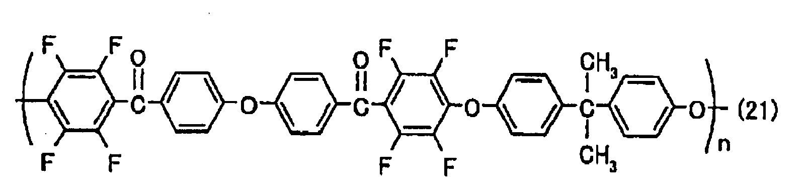
- In addition, an example of polyamide or polyester includes polyamide or polyester disclosed in
JP 10-508048 A 
- In the above formula (22), Y represents O or NH. E represents at least one selected from a covalent bond, an alkylene group having 2 carbon atoms, a halogenated alkylene group having 2 carbon atoms, a CH2 group, a C(CX3)2 group (wherein, X is a halogen or hydrogen), a CO group, an O atom, an S atom, an SO2 group, an Si(R)2 group, and an N (R) group, for example. A plurality of Es may be the same or different from each other. In E, R is at least one of an alkyl group having 1 to 3 carbon atoms and a halogenated alkyl group having 1 to 3 carbon atoms, and is located in a meta or para position with respect to a carbonyl functional group or a Y group.
- In the above formula (22), A and A' each represent a substituent, and t and z represent the numbers of the respective substituents. p represents an integer of 0 to 3, and q represents an integer of 1 to 3. r represents an integer of 0 to 3.
- A is selected from hydrogen, a halogen, an alkyl group having 1 to 3 carbon atoms, a halogenated alkyl group having 1 to 3 carbon atoms, an alkoxy group represented by OR (wherein, R is defined as above), an aryl group, a substituted aryl group prepared through halogenation or the like, an alkoxycarbonyl group having 1 to 9 carbon atoms, an alkylcarbonyloxy group having 1 to 9 carbon atoms, an aryloxycarbonyl group having 1 to 12 carbon atoms, an arylcarbonyloxy group having 1 to 12 carbon atoms and its substituted derivatives, an arylcarbamoyl group having 1 to 12 carbon atoms, and arylcarbonylamino group having 1 to 12 carbon atoms and its substituted derivatives, for example. A plurality of As may be the same or different from each other. A' is selected from a halogen, an alkyl group having 1 to 3 carbon atoms, a halogenated alkyl group having 1 to 3 carbon atoms, a phenyl group, and a substituted phenyl group, for example. A plurality of A's may be the same or different from each other. Examples of the substituent on a phenyl ring of the substituted phenyl group include a halogen, an alkyl group having 1 to 3 carbon atoms, a halogenated alkyl group having 1 to 3 carbon atoms, and the combination thereof. t represents an integer of 0 to 4, and z represents an integer of 0 to 3.
- The repeating unit of the polyamide or polyester represented by the above formula (22) is preferably a repeating unit represented by the following general formula (23).

- In the above formula (23), A, A', and Y are defined as those in the above formula (22). v represents an integer of 0 to 3, preferably an integer of 0 to 2. x and y are each 0 or 1, but are not both 0.
- Next, description will be given of a method of producing the second optical compensation layer. Any appropriate method may be employed as the method of producing the second optical compensation layer as long as the effect of the present invention can be provided.
- A solution of at least one polymer selected from the group consisting of polyamide, polyimide, polyester, polyetherketone, polyamideimide, and polyesterimide is applied to a transparent polymer film and is dried to form the polymer layer on the transparent polymer film. Then, the transparent polymer film and the polymer layer may be stretched or contracted integrally, to thereby obtain the second optical compensation layer.
- Examples of the solvent of the coating solution (a polymer solution to be applied to a transparent polymer film) include, but not limited to: halogenated hydrocarbons such as chloroform, dichloromethane, carbon tetrachloride, dichloroethane, tetrachloroethane, trichloroethylene, tetrachloroethylene, chlorobenzene, and ortho-dichlorobenzene; phenols such as phenol and parachlorophenol; aromatic hydrocarbons such as benzene, toluene, xylene, methoxybenzene, and 1,2-dimethoxybenzene; ketone-based solvents such as acetone, methyl ethyl ketone, methyl isobutyl ketone, cyclohexanone, cyclopentanone, 2-pyrrolidone, and N-methyl-2-pyrrolidone; ester-based solvents such as ethyl acetate and butyl acetate; alcohol-based solvents such as t-butyl alcohol, glycerine, ethylene glycol, triethylene glycol, ethylene glycol monomethylether, diethylene glycol dimethylether, propylene glycol, dipropylene glycol, and 2-methyl-2,4-pentanediol; amide-based solvents such as dimethylformamide and dimethylacetamide; nitrile-based solvents such as acetonitrile and butyronitrile; ether-based solvents such as diethyl ether, dibutyl ether, and tetrahydrofurane; carbon disulfide; ethyl cellosolve; and butyl cellosolve. Of those, methyl isobutyl ketone is preferred, because non-liquid crystal materials exhibits high solubility in the solvent and the solvent does not corrode the substrate. Each of those solvents can be used alone, or two or more of them can be used in combination.
- The application solution may have any appropriate concentration of the non-liquid crystalline polymer as long as the above-mentioned optical compensation layer can be obtained and the application solution may be applied. For example, the solution contains preferably 5 to 50 parts by weight, and more preferably 10 to 40 parts by weight of the non-liquid crystalline polymer with respect to 100 parts by weight of the solvent. The solution having a concentration within the above ranges has a viscosity allowing easy application.
- The application solution may further contain various additives such as a stabilizer, a plasticizer, and metals as required.
- The application solution may further contain another different resin as required. Examples of another different resin include various general-purpose resins, engineering plastics, a thermoplastic resin, and a thermosetting resin. Such a resin is used in combination, to thereby allow formation of an optical compensation layer having appropriate mechanical strength or durability in accordance with the purpose.
- Examples of the general-purpose resin include polyethylene (PE), polypropylene (PP), polystyrene (PS),polymethylmethacrylate (PMMA), an ABS resin, and an AS resin. Examples of the engineering plastic include polyacetate (POM), polycarbonate (PC), polyamide (PA: nylon), polyethylene terephthalate (PET), and polybutylene terephthalate (PBT). Examples of the thermoplastic resin include polyphenylene sulfide (PPS), polyether sulfone (PES), polyketone (PK), polyimide (PI), polycyclohexane dimethanol terephthalate (PCT), polyallylate (PAR), and a liquid crystal polymer (LCP). Examples of the thermosetting resin include an epoxy resin and a phenol novolac resin.
- The type and amount of another different resin to be added to the application solution may appropriately be set in accordance with the purpose. For example, such a resin is added to the non-liquid crystalline polymer in a ratio of preferably 0 to 50 mass%, and more preferably 0 to 30 mass%.
- Examples of a method of applying the solution include: a spin coating method; a roll coating method; a flow coating method; a printing method; a dip coating method; a flow casting method; a bar coating method; and a gravure printing method. For application, a polymer layer superposition method may also be used as required.
- After application, the solvent in the above-mentioned solution is evaporated and removed by drying such as natural drying, air drying, or heat drying (at 60 to 250°C, for example), to thereby form a film-like optical compensation layer.
- The same film as that used for a protective layer to be described below may be used as the transparent polymer film.
- The second optical compensation layer may be used by peeling the first optical compensation layer off from the laminate (laminate having the first optical compensation layer formed on the transparent polymer film) obtained as described above, or used as the laminate itself. In the case where the second optical compensation layer is used as a laminate and is further laminated with a polarizer, the transparent polymer film in the laminate may serve as a protective film of a polarizer to be described below.
- In the prevent invention, the first polarizing plate includes a first polarizer, and the second polarizer includes a second polarizer. Any appropriate polarizer may be employed as the first polarizer and the second polarizer used in the present invention depending on the purpose. Examples thereof include: a film prepared by adsorbing a dichromatic substance such as iodine or a dichromatic dye on a hydrophilic polymer film such as a polyvinyl alcohol-based film, a partially formalized polyvinyl alcohol-based film, or a partially saponified ethylene/vinyl acetate copolymer-based film and uniaxially stretching the film; and a polyene-based aligned film such as a dehydrated product of a polyvinyl alcohol-based film or a dehydrochlorinated product of a polyvinyl chloride-based film. Of those, a polarizer prepared by adsorbing a dichromatic substance such as iodine on a polyvinyl alcohol-based film and uniaxially stretching the film is particularly preferred because of its high polarized dichromaticity. A thickness of such a polarizer is generally, but not limited to, about 5 to 80 µm.
- The polarizer prepared by adsorbing iodine on a polyvinyl alcohol-based film and uniaxially stretching the filmmay be produced by, for example: immersing a polyvinyl alcohol-based film in an aqueous solution of iodine for coloring; and stretching the film to a 3 to 7 times length of the original length. The aqueous solution may contain boric acid, zinc sulfate, zinc chloride, or the like as required, or the polyvinyl alcohol-based film may be immersed in an aqueous solution of potassium iodide or the like. Further, the polyvinyl alcohol-based film may be immersed and washed in water before coloring as required. Washing the polyvinyl alcohol-based film with water not only allows removal of contamination on a film surface or washing away of an antiblocking agent, but also provides an effect of preventing unevenness such as uneven coloring by swelling of the polyvinyl alcohol-based film. The stretching of the film may be performed after coloring of the film with iodine, performed during coloring of the film, or performed followed by coloring of the film with iodine. The stretching may be performed in an aqueous solution of boric acid, potassium iodide, or the like, or in a water bath.
- The protective layer is preferably transparent and colorless. The protective layer may employ any appropriate protective layer as long as it is capable of protecting a polarizer without inhibiting the effects of the present invention. Typical examples thereof include the following protective layers (1) to (3).
- The in-plane retardation Δnd(550) of a protective layer (1) is preferably 0 nm or more and 10 nm or less, and more preferably 0 nm or more and 8 nm or less. The thickness direction retardation Rth(550) of the protective layer (1) is preferably 10 nm or more and 80 nm or less, more preferably 40 nm or more and 80 nm or less, and furthermore preferably 45 nm or more and 70 nm or less.
- The thickness of the protective layer (1) may appropriately be set in accordance with the purpose. Specifically, the thickness is preferably 20 to 140 µm, more preferably 40 to 120 µm, and furthermore preferably 60 to 100 µm.
- A material used for forming the protective layer (1) may employ any appropriate material. An example of the material is a plastic film having excellent transparency, mechanical strength, heat stability, moisture barrier properties, and the like. Specific examples of a resin used for forming the plastic film include an acetate resin such as triacetyl cellulose (TAC), a polyester resin, a polyether sulfone resin, a polysulfone resin, a polycarbonate resin, a polyamide resin, a polyimide resin, a polyolefin resin, an acrylic resin, a polynorbornene resin, a cellulose resin, a polyallylate resin, a polystyrene resin, a polyvinyl alcohol resin, a polyacrylic resin, and a mixture thereof. Further, an acrylic, urethane-based, acryl urethane-based, epoxy-based, silicone-based, etc. heat-curable resin or UV-curable resin may also be used. From viewpoints of polarization properties and durability, a TAC film having a surface subj ected to saponification treatment with an alkali or the like is preferred.
- The in-plane retardation Δnd(550) of a protective layer (2) is preferably 0 nm or more and 10 nm or less, more preferably 0 nm or more and 6 nm or less, and furthermore preferably 0 nm or more and 3 nm or less. The thickness direction retardation Rth (550) of the protective layer (2) is preferably 0 nm or more and 20 nm or less, more preferably 0 nm or more and 10 nm or less, furthermore preferably 0 nm or more and 6 nm or less, and particularly preferably 0 or more and 3 or less.
- The thickness of the protective layer (2) may appropriately be set in accordance with the purpose. Specifically, the thickness is preferably 20 to 200 µm, more preferably 30 to 100 µm, and furthermore preferably 35 to 95 µm.
a cellulose-based film is typically used as the protective layer (2) . Acellulose-based filmhaving a large thickness direction retardation (Rth) is subjected to appropriate treatment for reducing the thickness direction retardation (Rth), to thereby favorably obtain the protective layer (2). - The treatment for reducing the thickness direction retardation (Rth) may employ any appropriate treatment method. Examples thereof include: a method involving attaching a substrate formed of polyethylene terephthalate, polypropylene, stainless steel, or the like and having a solvent such as cyclopentanone or methyl ethyl ketone applied thereto together with a general cellulose-based film, drying the whole under heating (at about 80 to 150°C for about 3 to 10 minutes), and peeling off the substrate film; and a method involving applying a solution containing a norbornene-based resin, an acrylic resin, or the like dissolved in a solvent such as cyclopentanone or methyl ethyl ketone to a general cellulose-based film, drying the whole under heating (at about 80 to 150°C for about 3 to 10 minutes), and peeling off the applied film.
- A preferred example of a material used for forming the cellulose-based resin is a fatty acid-substituted cellulose-based polymer such as diacetyl cellulose or triacetyl cellulose. Generally used triacetyl cellulose has a degree of acetic acid substitution of about 2.8. However, the degree of acetic acid substitution is preferably controlled to 1.8 to 2.7, and the degree of propionic acid substitution is more preferably controlled to 0.1 to 1, to thereby reduce the thickness direction retardation (Rth).
- A plasticizer such as dibutyl phthalate, p-toluenesulfonanilide, or acetyl triethyl citrate may be added to the aliphatic acid-substituted cellulose-based polymer, to thereby allow control of the thickness direction retardation (Rth) to a small value. An addition amount of the plasticizer is preferably 40 parts by weight or less, more preferably 1 to 20 parts by weight, and furthermore preferably 1 to 15 parts by weight with respect to 100 parts by weight of the aliphatic acid-substituted cellulose-based polymer.
- The above-mentioned techniques for reducing the thickness direction retardation (Rth) to a small value may appropriately be used in combination.
- Another preferred specific example of the protective layer (2) is an acrylic resin film. A preferred example of the acrylic resin film is an acrylic resin film containing as a main component an acrylic resin (A) having a glutaric anhydride unit represented by the following structural formula (24) and described in
JP 2005-314534 A 
- In the acrylic resin (A), a ratio of the glutaric anhydride unit represented by the structural formula (24) is preferably 20 to 40 wt%, and more preferably 25 to 35 wt%.
- The acrylic resin (A) may contain one or two or more types of appropriate monomer units in addition to the glutaric anhydride unit represented by the structural formula (24). Apreferredexample of the monomer unit is a vinyl carboxylic acid alkyl ester unit. In the acrylic resin (A), a ratio of the vinyl carboxylic acid alkyl ester unit is preferably 60 to 80 wt%, and more preferably 65 to 75 wt%.
- An example of the vinyl carboxylic acid alkyl ester unit is a unit represented by the following general formula (25). In the following general formula (25): R3 represents a hydrogen atom or an aliphatic or alicyclic hydrocarbon having 1 to 5 carbon atoms; and R4 represents an aliphatic hydrocarbon having 1 to 5 carbon atoms.

- The acrylic resin (A) preferably has a weight average molecular weight of 80,000 to 150,000.
- A ratio of the acrylic resin (A) in the acrylic resin film is preferably 60 to 90 wt%.
- The acrylic resin film may contain one or two or more types of appropriate components in addition to the acrylic resin (A). Any appropriate component may be employed within a range not inhibiting the purpose of the present invention. Examples of the appropriate component include a resin except the acrylic resin (A), a UV absorber, an antioxidant, a lubricant, a plasticizer, a releasing agent, a color protection agent, a flame retardant, a nucleator, an antistatic agent, a pigment, and a colorant.
- A polymer film formed of a resin composition as described in
JP 2001-343529 A WO 01/37007 - Hereinafter, the present invention will be described more specifically by way of examples, but the present invention is not limited to the examples. Methods of measuring properties in examples are described below.
- Unless other methods are particularly described, refractive indices nx, ny, and nz of a sample film were measured with a spectroscopic ellipsometer (M-220, manufactured by JASCO Corporation), and in-plane retardations And and thickness direction retardations Rth were calculated. Measurement wavelengths were 380 nm, 550 nm, and 780 nm.
- A photoelastic coefficient of the sample film was measured with a spectroscopic ellipsometer (M-220, manufactured by JASCO Corporation).
- A liquid was dropped on a substrate by using a solid-liquid interface analyzer ("Drop Master 300", trade name, manufactured by Kyowa Interface Science Co., Ltd.), and a contact angle after 5 seconds was measured. Measuring conditions were for static contact angle measurement. Ultrapure water was used as water, and a liquid drop was 0.5 µl. The measurement was repeated 10 times for each substrate, and an average value of the measurements was used as a measured value.
- A brightness of a liquid crystal panel was measured by using a brightness measuring device ("CA-1500", trade name, manufactured by Konica Minolta Holdings, Inc.). Specifically, the measurement was conducted as described below. First, a liquid crystal panel was taken out of a liquid crystal display apparatus "BRAVIA 40-inch X-series" manufactured by Sony Corporation, and polarizing plates attached above and below a liquid crystal cell of the liquid crystal panel were peeled off. Then, polarizing plates produced in Examples or Comparative Examples were attached to both sides of the liquid crystal cell instead through an acrylicpressure-sensitive adhesive, to thereby produce a new liquid crystal panel. The produced liquid crystal panel was re-installed in the liquid crystal display apparatus, and the resultant was left standing under conditions of 60°C and 95% RH for 250 hours. Then, the whole was left standing at room temperature for 3 hours, and left standing for 3 hours while backlight was turned on. Unevenness in brightness of the liquid crystal panel was evaluated at a measuring distance of 1 m. The evaluation of unevenness in brightness was conducted by measuring the brightness of a white part and a black display part. Measurement positions of the white part and the black display part were as described below.
White part: point inside liquid crystal panel at 1/30 length of long side and 1/30 length of short side from corner
Black display part: point at center of liquid crystal panel - A cellulose ester film (available from Kaneka Corporation, trade name: KA, DSac (degree of acetyl substitution) = 0.04, DSpr (degree of propionyl substitution) = 2.76) having a thickness of 70 µm was stretched at a free end to a 1.5 times length at 145°C, to thereby obtain a first optical compensation layer having a thickness of 68 µm. The obtained first optical compensation layer had a photoelastic coefficient of 25x10-12 (m2/N) . The obtained first optical compensation layer had in-plane retardations Δnd(380) of 65 nm, Δnd(550) of 90 nm, andAnd(780) of 105 nm and thickness direction retardations Rth(380) of 69 nm, Rth(550) of 95 nm, and Rth(780) of 111 nm. The obtained first optical compensation layer had a refractive index profile of nx > ny ≈ nz at 550 nm.
- The first optical compensation layer obtained as described above was attached to a polarizing plate (available from Nitto Denko Corporation, trade name: SEG1224) having a structure of TAC protective film (available from FUJIFILM Corporation, trade name: TF80UL) /polarizer/TAC protective film (trade name: TF80UL) through a pressure-sensitive adhesive (thickness of 20 µm), to thereby obtain a polarizing plate provided with a first optical compensation layer. At this time, lamination was conducted such that a slow axis of the first optical compensation layer and a stretching axis (absorption axis) of the polarizer were substantially perpendicular to each other.
- Polyimide synthesized from 2,2-bis(3,4-dicarboxyphenyl) hexafluoropropane dianhydride (6FDA) and 2,2'-bis(trifluoromethyl)-4,4'-diaminobiphenyl (TFMB) was dissolved in methyl isobutyl ketone (MIBK), to thereby prepare a 15 mass% polyimide solution. This solution was applied to a triacetyl cellulose substrate (transparent polymer film) to a thickness of 30 µm. Then, the whole was subjected to drying treatment at 100°C for 10 minutes, to thereby obtain a second optical compensation layer having a thickness of about 4 µm. The obtained second optical compensation layer had in-plane retardations And(380) of 0.4 nm, Δnd (550) of 0.3 nm, and Δnd(780) of 0.3 nm and thickness direction retardations Rth(380) of 178 nm, Rth(550) of 120 nm, and Rth(780) of 110 nm. The obtained second optical compensation layer had a refractive index profile of nx ≈ ny >,nz at 550 nm.
- The second optical compensation layer obtained as described above was attached to a polarizing plate (available from Nitto Denko Corporation, trade name: SEG1224) through a pressure-sensitive adhesive (thickness of 20 µm), to thereby obtain a polarizing plate provided with a second optical compensation layer.
- A waterproof agent (available from Daikin Industries, Ltd., fluorine-based releasing agent, trade name: DAIFREE GA-6010) was sprayed to an entire side surface of each of the polarizing plate provided with a first optical compensation layer and the polarizing plate provided with a second optical compensation layer as described above for waterproof treatment. A water contact angle of each of waterproof parts was 116°.
- The brightness was measured by using the polarizing plate provided with a first optical compensation layer and the polarizing plate provided with a second optical compensation layer which are subjected to the waterproof treatment. Attachment of the polarizing plate provided with a first optical compensation layer and the polarizing plate provided with a second optical compensation layer to a liquid crystal cell was conducted by attaching the polarizing plate provided with a first optical compensation layer to a viewer side of the liquid crystal cell through an acrylic pressure-sensitive adhesive such that the first optical compensation layer was arranged on a liquid crystal cell side. Further, the polarizing plate provided with a second optical compensation layer was attached to a backlight side of the liquid crystal cell through an acrylic pressure-sensitive adhesive such that the second optical compensation layer was arranged on the liquid crystal cell side. Lamination was conducted such that a stretching (absorption) axis of the polarizer of the polarizing plate provided with a first optical compensation layer and a stretching (absorption) axis of the polarizer of the polarizing plate provided with a second optical compensation layer were substantially perpendicular to each other, to thereby obtain a liquid crystal panel. As a result of measurement, the brightness of a white part was 0.53 cd/m2, and the brightness of a black display part was 0.47 cd/m2. Fig. 5 shows a state of the liquid crystal panel during the brightness measurement.
- The same procedure as that of Example 1 was conducted except that the polarizing plate provided with a first optical compensation layer and the polarizing plate provided with a second optical compensation layer were not subjected to the waterproof treatment in Example 1. The polarizing plate provided with a first optical compensation layer and the polarizing plate provided with a second optical compensation layer not subjected to the waterproof treatment each had a water contact angle of 35° on each side surface. As a result of brightness measurement, the brightness of the white part was 0.80 cd/m2, and the brightness of the black display part was 0.45 cd/m2. Fig. 6 shows a state of the liquid crystal panel during the brightness measurement.
- In comparison of Figs. 5 and 6, no unevenness in brightness was observed in the liquid crystal panel of Example 1 employing the polarizing plate subjected to the waterproof treatment, but significant unevenness in brightness was observed in the liquid crystal panel of Comparative Example 1 employing the polarizing plate not subjected to the waterproof treatment.
- A waterproof agent (available from Daikin Industries, Ltd., fluorine-based releasing agent, trade name: DAIFREE GA-6010) was sprayed to an entire side surface of polarizing plates "NIBCOM-NXP" and "SEG1224" both available from Nitto Denko Corporation for waterproof treatment. The water contact angle of each of waterproof parts was 116°.
- Next, "NIBCOM-NXP" was attached to a backlight side of a liquid crystal cell taken out of a liquid crystal TV "BRAVIA 4 0-inch X-series" manufactured by Sony Corporation by using an acrylic pressures-sensitive adhesive (thickness of 20 µm), and "SEG1224" was attached to a viewer side thereof, to thereby produce a liquid crystal panel. Lamination was conducted such that a stretching (absorption) axis of a polarizer of "NIBCOM-NXP" and a stretching (absorption) axis of a polarizer of "SEG1224" were substantially perpendicular to each other.
- The brightness of the obtained liquid crystal panel was measured. Fig. 7 shows a state of the liquid crystal panel during the brightness measurement.
- The same procedure as that of Example 2 was conducted except that "NIBCOM-NXP" and "SEG1224" were not subjected to the waterproof treatment in Example 2.
- The brightness of the obtained liquid crystal panel was measured. Fig. 8 shows a state of the liquid crystal panel during the brightness measurement.
- In comparison of Figs. 7 and 8, no unevenness in brightness was observed in the liquid crystal panel of Example 2 employing the polarizing plate subjected to the waterproof treatment, but significant unevenness in brightness was observed in the liquid crystal panel of Comparative Example 2 employing the polarizing plate not subjected to the waterproof treatment.
- A waterproof agent.(available from Daikin Industries, Ltd. , fluorine-based releasing agent, trade name: DAIFREE GA-6010) was sprayed to an entire side surface of polarizing plates "NIBCOM-NXP" and "VEG1722" both available from Nitto Denko Corporation for waterproof treatment. The water contact angle of each of waterproof parts was 116°.
- Next, "NIBCOM-NXP" was attached to a backlight side of a liquid crystal cell taken out of a liquid crystal TV "BRAVIA 4 0-inchX-series" manufactured by Sony Corporation by using an acrylic pressures-sensitive adhesive (thickness of 20 µm), and "VEG1722" was attached to a viewer side thereof, to thereby produce a liquid crystal panel. Lamination was conducted such that a stretching (absorption) axis of a polarizer of "NIBCOM-NXP" and a stretching (absorption) axis of a polarizer of "VEG1722" were substantially perpendicular to each other.
- The brightness of the obtained liquid crystal panel was measured. Fig. 9 shows a state of the liquid crystal panel during the brightness measurement.
- The same procedure as that of Example 3 was conducted except that "NIBCOM-NXP" and "VEG1722" were not subjected to the waterproof treatment in Example 3.
- The brightness of the obtained liquid crystal panel was measured. Fig. 10 shows a state of the liquid crystal panel during the brightness measurement.
- In comparison of Figs. 9 and 10, no unevenness in brightness was observed in the liquid crystal panel of Example 3 employing the polarizing plate subjected to the waterproof treatment, but significant unevenness in brightness was observed in the liquid crystal panel of Comparative Example 3 employing the polarizing plate not subjected to the waterproof treatment.
- A norbornene-based film "Arton" available from JSR Corporation was stretched to a 3 times length at 145°C. The retardation values of the film were measured by using "KOBRA-21ADH" manufactured by Oji Scientific Instruments. The film had Δnd of 115 nm and Rth of 135 nm.
- Next, the norbornene-based film was attached to one .side of a polarizer available from Nitto Denko Corporation, and a triacetyl cellulose film (thickness of 40 µm) available from FUJIFILM Corporation was attached to an opposite side of the polarizer, to thereby produce a polarizing plate (A). A waterproof agent (available from Daikin Industries, Ltd., fluorine-based releasing agent, trade name: DAIFREE GA-6010) was sprayed to an entire side surface of the obtained polarizing plate (A) for waterproof treatment. The water contact angle of a waterproof part was 116°.
- Meanwhile, a primer (polyester urethane) was applied to a triacetyl cellulose film (thickness of 40 µm) available from FUJIFILM Corporation, and a 15% solution of polyimide synthesized from 2,2'-bis(3,4-dicarboxyphenyl) hexafluoropropane and 2,2'-bis(trifluoromethyl)-4,4'-diaminobiphenyl by using cyclohexane as a solvent was applied thereto to a thickness of about 20 µm. Then, the whole was subjected to drying treatment at 100 °C for 10 minutes, to thereby obtain a polyimide thin film having a thickness of about 3.2 µm. The retardation values of the obtained composite retardation film were measured by using "KOBRA-21ADH" manufactured by Oji Scientific Instruments. The film had Δnd of 1 nm and Rth of 183 nm. Next, the composite retardation film instead of the triacetyl cellulose film was attached to one side of the polarizing plate "SEG1224" available from Nitto Denko Corporation through a polyvinyl alcohol-based adhesive such that the polyimide thin film was arranged on an outer side, to thereby obtain a polarizing plate (B). In the polarizing plate (B), a slow axis of the polyimide thin film and an absorption axis of the polarizer were perpendicular to each other. Awaterproofagent (availablefromDaikinIndustries, Ltd., fluorine-based releasing agent, trade name: DAIFREE GA-6010) was sprayed to an entire side surface of the polarizing plate (B) for waterproof treatment. The water contact angle of a waterproof part was 116°.
- Next, the polarizing plate (A) was attached to a viewer side of a liquid crystal cell taken out of a liquid crystal TV "BRAVIA 40-inch X-series" manufactured by Sony Corporation by using an acrylic pressures-sensitive adhesive (thickness of 20 µm) such that the norbornene-based film was arranged on a cell side, and the polarizing plate (B) was attached to a backlight side thereof such that the polyimide thin film was arranged on the cell side, to thereby produce a liquid crystal panel. Lamination was conducted such that a stretching (absorption) axis of a polarizer of the polarizing plate (A) and a stretching (absorption) axis of a polarizer of the polarizing plate (B) were substantially perpendicular to each other.
- The brightness of the obtained liquid crystal panel was measured. Fig. 11 shows a state of the liquid crystal panel during the brightness measurement.
- The same procedure as that of Example 4 was conducted except that the polarizing plate (A) and the polarizing plate (B) were not subjected to the waterproof treatment in Example 4.
- The brightness of the obtained liquid crystal panel was measured. Fig. 12 shows a state of the liquid crystal panel during the brightness measurement.
- In comparison of Figs. 11 and 12, no unevenness in brightness was observed in the liquid crystal panel of Example 4 employing the polarizing plate subjected to the waterproof treatment, but significant unevenness in brightness was observed in the liquid crystal panel of Comparative Example 4 employing the polarizing plate not subjected to the waterproof treatment.
- The liquid crystal panel and liquid crystal display apparatus including the liquid crystal panel of the present invention may suitably be used for a liquid crystal television, a cellular phone, or the like.
- Many other modifications will be apparent to and be readily practiced by those skilled in the art without departing from the scope and spirit of the invention. It should therefore be understood that the scope of the appended claims is not intended to be limited by the details of the description but should rather be broadly construed.
Claims (8)
- A liquid crystal panel comprising: a liquid crystal cell; a first polarizing plate arranged on one side of the liquid crystal cell; and a second polarizing plate arranged on another side of the liquid crystal cell, wherein:the first polarizing plate comprises a first polarizer;the second polarizing plate comprises a second polarizer; andthe first polarizing plate comprises a first waterproof part on at least a part of a side surface, and/or the second polarizing plate comprises a second waterproof part on at least a part of a side surface.
- A liquid crystal panel according to claim 1, wherein: the first polarizing plate has a substantially rectangular shape; and the first waterproof part includes four corners of the first polarizing plate.
- A liquid crystal panel according to claim 1 or 2, wherein the first waterproof part is provided on an entire side surface of the first polarizing plate.
- A liquid crystal panel according to any one of claims 1 to 3, wherein: the second polarizing plate has a substantially rectangular shape; and the second waterproof part includes four corners of the second polarizing plate.
- A liquid crystal panel according to any one of claims 1 to 4, wherein the second waterproof part is provided on an entire side surface of the second polarizing plate.
- A liquid crystal panel according to any one of claims 1 to 5, wherein the first waterproof part and the second waterproof part each have a water contact angle of 80° or more.
- A liquid crystal panel according to any one of claims 1 to 6, wherein the liquid crystal cell is of VA mode or OCB mode.
- A liquid crystal display apparatus comprising the liquid crystal panel according to any one of claims 1 to 7.
Applications Claiming Priority (2)
| Application Number | Priority Date | Filing Date | Title |
|---|---|---|---|
| JP2006124985 | 2006-04-28 | ||
| JP2007001497A JP2007316587A (en) | 2006-04-28 | 2007-01-09 | Liquid crystal panel and liquid crystal display device |
Publications (1)
| Publication Number | Publication Date |
|---|---|
| EP1850169A1 true EP1850169A1 (en) | 2007-10-31 |
Family
ID=38006920
Family Applications (1)
| Application Number | Title | Priority Date | Filing Date |
|---|---|---|---|
| EP07008014A Withdrawn EP1850169A1 (en) | 2006-04-28 | 2007-04-19 | Liquid crystal panel |
Country Status (5)
| Country | Link |
|---|---|
| US (1) | US20070252925A1 (en) |
| EP (1) | EP1850169A1 (en) |
| JP (1) | JP2007316587A (en) |
| KR (1) | KR20070106401A (en) |
| TW (1) | TW200809275A (en) |
Families Citing this family (5)
| Publication number | Priority date | Publication date | Assignee | Title |
|---|---|---|---|---|
| JP5473840B2 (en) | 2010-09-08 | 2014-04-16 | 日東電工株式会社 | Liquid crystal panel and liquid crystal display device |
| US20160124264A1 (en) * | 2014-11-05 | 2016-05-05 | Shenzhen China Star Optoelectronics Technology Co. Ltd. | Compensation structure for liquid crystal panels and the liquid crystal displays |
| KR102453566B1 (en) * | 2015-06-01 | 2022-10-13 | 삼성디스플레이 주식회사 | Display device and manufacturing method thereof |
| CN106373669A (en) * | 2016-10-10 | 2017-02-01 | 福建农林大学 | A preparation method of cellulose-based aluminum-doped zinc oxide transparent conductive material |
| TWI856514B (en) * | 2022-02-11 | 2024-09-21 | 南韓商Lg化學股份有限公司 | Optical device |
Citations (2)
| Publication number | Priority date | Publication date | Assignee | Title |
|---|---|---|---|---|
| US20040212884A1 (en) * | 2003-02-25 | 2004-10-28 | Masayuki Satake | Optical member, method for producing the same, adhesive optical member and image viewing display |
| EP1489437A1 (en) * | 2003-06-16 | 2004-12-22 | Nitto Denko Corporation | Laminated optical film, elliptically polarizing plate, and image viewing display |
Family Cites Families (5)
| Publication number | Priority date | Publication date | Assignee | Title |
|---|---|---|---|---|
| JPH08320485A (en) * | 1995-05-26 | 1996-12-03 | Rohm Co Ltd | Liquid crystal display device |
| TWI296727B (en) * | 2001-09-19 | 2008-05-11 | Nitto Denko Corp | Polarizing plate and method of manufacturing the same, and liquid crystal display using the polarizing plate |
| US7379131B2 (en) * | 2003-03-28 | 2008-05-27 | Fujifilm Corporation | Liquid crystal display device |
| JP2005031621A (en) * | 2003-06-16 | 2005-02-03 | Nitto Denko Corp | Optical film, polarizing optical film, and image display device |
| TW200624883A (en) * | 2004-12-24 | 2006-07-16 | Innolux Display Corp | Polarizer and display panel using the same |
-
2007
- 2007-01-09 JP JP2007001497A patent/JP2007316587A/en active Pending
- 2007-03-27 TW TW096110570A patent/TW200809275A/en unknown
- 2007-04-16 KR KR1020070036958A patent/KR20070106401A/en not_active Ceased
- 2007-04-19 EP EP07008014A patent/EP1850169A1/en not_active Withdrawn
- 2007-04-27 US US11/790,729 patent/US20070252925A1/en not_active Abandoned
Patent Citations (2)
| Publication number | Priority date | Publication date | Assignee | Title |
|---|---|---|---|---|
| US20040212884A1 (en) * | 2003-02-25 | 2004-10-28 | Masayuki Satake | Optical member, method for producing the same, adhesive optical member and image viewing display |
| EP1489437A1 (en) * | 2003-06-16 | 2004-12-22 | Nitto Denko Corporation | Laminated optical film, elliptically polarizing plate, and image viewing display |
Also Published As
| Publication number | Publication date |
|---|---|
| KR20070106401A (en) | 2007-11-01 |
| JP2007316587A (en) | 2007-12-06 |
| TW200809275A (en) | 2008-02-16 |
| US20070252925A1 (en) | 2007-11-01 |
Similar Documents
| Publication | Publication Date | Title |
|---|---|---|
| JP3883134B2 (en) | Liquid crystal display | |
| KR100822248B1 (en) | Liquid crystal panel and liquid crystal display | |
| EP1850169A1 (en) | Liquid crystal panel | |
| CN101310214B (en) | Liquid crystal display device | |
| US20060238684A1 (en) | Liquid crystal panel and liquid crystal display apparatus | |
| JP3950468B2 (en) | Liquid crystal display | |
| JP3967764B2 (en) | Liquid crystal panel and liquid crystal display device | |
| US20090279031A1 (en) | Liquid crystal panel and liquid crystal display apparatus using the same | |
| KR100916738B1 (en) | Liquid crystal panel and liquid crystal display | |
| JP4640929B2 (en) | Liquid crystal display device | |
| US7944531B2 (en) | Liquid crystal panel and liquid crystal display apparatus | |
| JP2007213093A (en) | Liquid crystal panel and liquid crystal display device | |
| US8194204B2 (en) | Liquid crystal panel and liquid crystal display apparatus using the same | |
| JP2007264588A (en) | Liquid crystal panel and liquid crystal display device using the same | |
| US20070013844A1 (en) | Liquid crystal panel and liquid crystal display using the same | |
| CN101317126A (en) | Liquid crystal panel and liquid crystal display device | |
| JP4911573B2 (en) | LCD panel | |
| CN101248385A (en) | Liquid crystal panel and liquid crystal display device using same |
Legal Events
| Date | Code | Title | Description |
|---|---|---|---|
| PUAI | Public reference made under article 153(3) epc to a published international application that has entered the european phase |
Free format text: ORIGINAL CODE: 0009012 |
|
| AK | Designated contracting states |
Kind code of ref document: A1 Designated state(s): AT BE BG CH CY CZ DE DK EE ES FI FR GB GR HU IE IS IT LI LT LU LV MC MT NL PL PT RO SE SI SK TR |
|
| AX | Request for extension of the european patent |
Extension state: AL BA HR MK YU |
|
| 17P | Request for examination filed |
Effective date: 20080430 |
|
| 17Q | First examination report despatched |
Effective date: 20080529 |
|
| AKX | Designation fees paid |
Designated state(s): AT BE BG CH CY CZ DE DK EE ES FI FR GB GR HU IE IS IT LI LT LU LV MC MT NL PL PT RO SE SI SK TR |
|
| STAA | Information on the status of an ep patent application or granted ep patent |
Free format text: STATUS: THE APPLICATION HAS BEEN WITHDRAWN |
|
| 18W | Application withdrawn |
Effective date: 20090211 |