EP1848129A1 - Multi-channel phase modulation method for suppression of intra-channel non-linear distortion - Google Patents
Multi-channel phase modulation method for suppression of intra-channel non-linear distortion Download PDFInfo
- Publication number
- EP1848129A1 EP1848129A1 EP06112780A EP06112780A EP1848129A1 EP 1848129 A1 EP1848129 A1 EP 1848129A1 EP 06112780 A EP06112780 A EP 06112780A EP 06112780 A EP06112780 A EP 06112780A EP 1848129 A1 EP1848129 A1 EP 1848129A1
- Authority
- EP
- European Patent Office
- Prior art keywords
- modulation
- approximately
- range
- phase
- value
- Prior art date
- Legal status (The legal status is an assumption and is not a legal conclusion. Google has not performed a legal analysis and makes no representation as to the accuracy of the status listed.)
- Withdrawn
Links
Images


Classifications
-
- H—ELECTRICITY
- H04—ELECTRIC COMMUNICATION TECHNIQUE
- H04B—TRANSMISSION
- H04B10/00—Transmission systems employing electromagnetic waves other than radio-waves, e.g. infrared, visible or ultraviolet light, or employing corpuscular radiation, e.g. quantum communication
- H04B10/25—Arrangements specific to fibre transmission
- H04B10/2507—Arrangements specific to fibre transmission for the reduction or elimination of distortion or dispersion
- H04B10/2543—Arrangements specific to fibre transmission for the reduction or elimination of distortion or dispersion due to fibre non-linearities, e.g. Kerr effect
- H04B10/2563—Four-wave mixing [FWM]
-
- H—ELECTRICITY
- H04—ELECTRIC COMMUNICATION TECHNIQUE
- H04B—TRANSMISSION
- H04B10/00—Transmission systems employing electromagnetic waves other than radio-waves, e.g. infrared, visible or ultraviolet light, or employing corpuscular radiation, e.g. quantum communication
- H04B10/50—Transmitters
- H04B10/516—Details of coding or modulation
- H04B10/5161—Combination of different modulation schemes
-
- H—ELECTRICITY
- H04—ELECTRIC COMMUNICATION TECHNIQUE
- H04B—TRANSMISSION
- H04B10/00—Transmission systems employing electromagnetic waves other than radio-waves, e.g. infrared, visible or ultraviolet light, or employing corpuscular radiation, e.g. quantum communication
- H04B10/50—Transmitters
- H04B10/516—Details of coding or modulation
- H04B10/54—Intensity modulation
- H04B10/541—Digital intensity or amplitude modulation
-
- H—ELECTRICITY
- H04—ELECTRIC COMMUNICATION TECHNIQUE
- H04B—TRANSMISSION
- H04B10/00—Transmission systems employing electromagnetic waves other than radio-waves, e.g. infrared, visible or ultraviolet light, or employing corpuscular radiation, e.g. quantum communication
- H04B10/50—Transmitters
- H04B10/516—Details of coding or modulation
- H04B10/548—Phase or frequency modulation
Definitions
- the present invention relates to a method for reducing distortion of data modulated optical signals in a plurality of wavelength channels in a WDM-transmission link and to an optical transmitter for use in an optical transmission network.
- Optical wavelength division multiplexed transmission systems typically operate at up to 10 Gb/s per channel.
- Growing demand for capacity in transmission systems is leading to a shortage of transmission capacity.
- a cost-effective and flexible solution to this problem is to add (or replace 10-Gb/s channels with) 40-Gb/s channels in transmission systems where more capacity is needed.
- the 40-Gb/s signals must be successfully transmitted on wavelength-division multiplexed (WDM), dispersion-managed (DM) transmission links designed and optimized for 10-Gb/s signals. This poses some challenges in terms of filtering, dispersion, and especially non-linear effects.
- WDM wavelength-division multiplexed
- DM dispersion-managed
- Return-to-Zero (RZ) signals are more tolerant to non-linear effects than Non-Return-to-Zero (NRZ) signals, and that for 40 Gbit/s signals the most critical non-linear impairments are intra-channel rather than inter-channel.
- Intra-channel impairments occur when two or more bits within one channel interfere with each other, thereby creating ghost pulses and amplitude jitter.
- RZ-signals in combination with appropriate phase modulation techniques.
- APRZ Alternate-Phase Return-to-Zero
- phase modulation signal For APRZ, synchronization between the phase modulation signal and the data signal is needed in order to obtain the desired phase alteration, e.g. the phase may alternate every second bit such as to decrease distortion due to intra-channel non-linear effects.
- a problem of methods proposed in the prior art is that each channel requires a separate phase modulator. Further, some of the proposed methods increase the spectral bandwidth of the signal, whereby filtering through a DWDM-multiplexer is rendered more difficult.
- an optical transmitter comprising a plurality of sources of modulated optical signals, a multiplexer coupled to each of the sources for receiving the modulated optical signal and transmitting the optical signals over a long fiber waveguide, a phase modulator for modulating the phase of the optical signals propagating through the long fiber waveguide and an optical amplifier for amplifying the phase-modulated optical signals as the optical signals propagate through the long fiber waveguide.
- the modulator being arranged after the multiplexer, all signals are modulated simultaneously.
- a method of modulating the phase of the optical signals at a modulation frequency that reduces the growth of four wave mixing (FWM) products that are otherwise generated along the length of the fiber.
- FWM four wave mixing
- the modulation waveform is a square wave.
- a problem of US patent no. 6,606,178 is that with the transmitter and method disclosed therein, intra-channel, non-linear distortion effects (i.e. distortion due to interference among bits within a channel) are present.
- An object of the present invention is to reduce distortion of data modulated optical signals caused by intra-channel non-linear effects in a plurality of wavelength channels in a WDM-transmission link.
- a method for modulating the phase of a plurality of wavelength channels spaced from each other by a channel spacing in a WDM-transmission link comprising the step of asynchronously modulating the plurality of channels.
- a modulation rate of the modulation is set to be in a range of approximately 20% to approximately 70% of a bit rate of any one of the channels.
- a modulation depth of the modulation is set to be in the range from zero to approximately the channel spacing divided by the modulation rate.
- an optical transmitter for use in an optical transmission network.
- the optical transmitter comprises a plurality of sources for generating modulated optical signals, each source representing a channel in a WDM-transmission link, wherein channels are spaced from each other by a channel spacing, a multiplexer connected to each of the sources for receiving the modulated optical signals and transmitting the modulated optical signals over the transmission link.
- the optical transmitter further comprises a phase modulator arranged to modulate the phase of the modulated optical signals, and an optical amplifier for amplifying the modulated optical signals.
- a modulation rate of the phase modulator is set to be in the range of approximately 20% to approximately 70% of a bit rate of any one of the modulated optical signals, and a modulation depth of the phase modulator is set to be in the range from zero to approximately the channel spacing divided by the modulation rate.
- the inventors have noted that by scrambling, i.e. asynchronously modulating, a phase and frequency shift of a plurality of data modulated optical signals by properly setting particular modulation parameters, reduction of intra-channel non-linear distortions is achieved. Intra-channel non-linear distortions are built up of a number of undesired interactions from different bits within the same channel.
- the inventors realized that by tuning parameters pertaining to modulation rate (or modulation frequency) and modulation depth to lie in a specific range, an improvement of the signal quality could be obtained.
- the modulation rate and the modulation depth of the phase modulation is set in a combination that, firstly, gives consecutive bits different phase or frequency, and that, secondly, results in a spectral broadening of single wavelength signals which is less than the channel spacing in order to make it possible to separate different signals in a demultiplexer at the receiver.
- the modulation rate should be less then the bit-rate.
- the modulation rate is tuned to lie in the range of 20% to 70% of the bit rate, since a receiver sensitivity improvement of more than 1.5 dB may be attained for a range of selected modulation depth values, as will be shown hereinafter.
- the modulation depth values range from zero to less than or equal to the channel spacing divided by the modulation frequency, which is explained in more detail hereinafter.
- the modulation depth it is preferred to set the modulation depth to approximately 0.4 ⁇ - ⁇ , most preferable to approximately 0.5 ⁇ - 0.9 ⁇ .
- these two modulation depth intervals imply a receiver sensitivity improvement of more than 1.5 dB and 3 dB, respectively.
- the receiver sensitivity improvement is further improved if the modulation rate is set to 35% to 65% of said bit rate. In this case, the receiver sensitivity improvement is 3 dB or more for chosen values of the modulation depth.
- the modulation rate may be adjustable in a range as specified above.
- the modulation depth may be adjustable in a range as specified above.
- FIG. 1 there is shown an apparatus 10 for transmitting an optical signal that includes a number of optical transmitters Tx 1...n , a wavelength multiplexer 12, a phase modulator 13 and an amplifier 14.
- Each optical transmitter Tx 1...n is clocked by a specific clock signal c 1...n and it generates an optical signal, which is modulated by an electrical data signal d 1...n at bit rate R 1...n , to be transmitted on a specific channel in a wavelength-division multiplexing (WDM) transmission system.
- WDM wavelength-division multiplexing
- Each transmitter is connected to an input port of the multiplexer 12, in which all connected signals are combined into one single multiplexed signal to be transmitted on one optical fiber 15.
- the multiplexed signal is then phase modulated by a phase modulator 13, which operates at a frequency f PM and is coupled to the output port of the wavelength multiplexer and to the input port of the booster amplifier 14.
- FIG. 1 there is shown an apparatus 16 for receiving an optical signal.
- the apparatus 16 comprises an amplifier 17, a demultiplexer 18 and a number of optical receivers Rx 1...n for receiving and converting the optical signals to electrical signals.
- the phase modulator 13 modulates the phase of the multiplexed optical signal.
- the electrical wave controlling the phase modulator is independent of the clock signals c 1...n employed for generating each respective signal. As a consequence, the phase modulation is asynchronous for each channel. It is preferred that the waveform of the modulation signal is periodical and has an inclined leading edge and an inclined trailing edge.
- phase-modulating signal has the form of a sine wave
- neighboring bit slots will have different phase and different frequency shifts.
- N 2
- phase and frequency shift would alternate between two values.
- the amplitude of this phase alternation and frequency-shift alternation would be constant throughout the signal. In the case of asynchronous phase modulation, this will be true only for bit slots close to each other, and only if the ratio between the bit rate and the phase-modulation frequency is approximately equal to N.
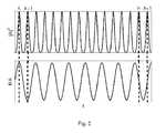
- Fig. 2 there is illustrated how the phase and frequency shift vary for different pulses, or bit slots.
- Fig. 2 In the topmost diagram of Fig. 2, there is shown the intensity of a number of pulses of an optical signal at bit rate R. For the sake of simplicity, all the pulses correspond to logical "ones".
- f PM and R will cause a progressive shift in the pulses illustrated in the topmost diagram in Fig. 2, so that away from bit slot k, the amplitude of the phase alternation and frequency-shift alternation will be different than ⁇ k and ⁇ k .
- condition A the build-up of ghost pulses and amplitude jitter is reduced because of alternating phase (as in APRZ).
- condition B the build-up of ghost pulses and amplitude jitter is reduced because the alternating frequency shift fulfills a frequency matching condition for reduction of intra-channel non-linear distortion.
- reduction of distortion due to non-linear intra-channel effects increases with increasing ⁇ .
- the spectral broadening is determined by the shifting of spectral components away from each other by an amount corresponding to the frequency-shift alternation, ⁇ pp f PM . If this shift exceeds the spectral range allocated to half the channel spacing, i.e. the channel spacing, S ch , a part of the spectrum will end up in the wavelength region allocated to the neighboring channel, and interference will take place. Therefore the following condition should be met: ⁇ pp f PM ⁇ S ch , or f PM ⁇ S ch / ⁇ pp .
- the transmission performance is evaluated in terms of power penalty, i.e. degradation in receiver sensitivity with respect to the sensitivity is obtained for a transmitter and a receiver with no transmission line therebetween.
- Receiver sensitivity is defined as the minimum power needed at the receiver in order to achieve a bit error ratio of 10 -9 .
- asynchronous phase modulation improves the non-linear tolerance in a approximate range of 0 ⁇ ⁇ ⁇ S ch / f PM .
- Performance improvement is very high for values of ⁇ pp,opt around 2 ⁇ / 3, and f PM,opt around 0.5 R, and slightly lower but still high within a range of ⁇ 40% from ⁇ pp,opt and f PM,opt .
- the values ⁇ pp,opt and f PM,opt will most likely change if the parameters of the optical system, such as pulse chirp, duty cycle, span length, dispersion map and launch power, are changed.
- the modulation rate is set (or is adjustable) in a range from approximately 35% to 65%, whereby the receiver sensitivity becomes greater than or equal to 3 dB.
- Fig. 4 shows a further result from a simulation, wherein the modulation depth is varied for three different phase-modulation frequencies: 24%, 49% and 73% of the bit rate R.
- receiver sensitivity improvement as a function of modulation depth over ⁇ is plotted.
- there is an improvement of the signal quality when the modulation depth is less than channel spacing divided by the modulation rate.
Landscapes
- Physics & Mathematics (AREA)
- Electromagnetism (AREA)
- Engineering & Computer Science (AREA)
- Computer Networks & Wireless Communication (AREA)
- Signal Processing (AREA)
- Nonlinear Science (AREA)
- Optical Communication System (AREA)
Abstract
Description
- The present invention relates to a method for reducing distortion of data modulated optical signals in a plurality of wavelength channels in a WDM-transmission link and to an optical transmitter for use in an optical transmission network.
- Optical wavelength division multiplexed transmission systems typically operate at up to 10 Gb/s per channel. Growing demand for capacity in transmission systems is leading to a shortage of transmission capacity. A cost-effective and flexible solution to this problem is to add (or replace 10-Gb/s channels with) 40-Gb/s channels in transmission systems where more capacity is needed. In order for this solution to be inexpensive and flexible, the 40-Gb/s signals must be successfully transmitted on wavelength-division multiplexed (WDM), dispersion-managed (DM) transmission links designed and optimized for 10-Gb/s signals. This poses some challenges in terms of filtering, dispersion, and especially non-linear effects. In the art, it is known that Return-to-Zero (RZ) signals are more tolerant to non-linear effects than Non-Return-to-Zero (NRZ) signals, and that for 40 Gbit/s signals the most critical non-linear impairments are intra-channel rather than inter-channel. Intra-channel impairments occur when two or more bits within one channel interfere with each other, thereby creating ghost pulses and amplitude jitter. In the past several attempts have been made to reduce the abovementioned intra-channel non-linear effects by using RZ-signals in combination with appropriate phase modulation techniques. For example, a modulation format referred to as Alternate-Phase Return-to-Zero (APRZ) has been proposed to decrease distortion. For APRZ, synchronization between the phase modulation signal and the data signal is needed in order to obtain the desired phase alteration, e.g. the phase may alternate every second bit such as to decrease distortion due to intra-channel non-linear effects. A problem of methods proposed in the prior art is that each channel requires a separate phase modulator. Further, some of the proposed methods increase the spectral bandwidth of the signal, whereby filtering through a DWDM-multiplexer is rendered more difficult.
- In
US patent no. 6,606,178 , there is disclosed an optical transmitter comprising a plurality of sources of modulated optical signals, a multiplexer coupled to each of the sources for receiving the modulated optical signal and transmitting the optical signals over a long fiber waveguide, a phase modulator for modulating the phase of the optical signals propagating through the long fiber waveguide and an optical amplifier for amplifying the phase-modulated optical signals as the optical signals propagate through the long fiber waveguide. As a consequence of the modulator being arranged after the multiplexer, all signals are modulated simultaneously. Further, there is disclosed a method of modulating the phase of the optical signals at a modulation frequency that reduces the growth of four wave mixing (FWM) products that are otherwise generated along the length of the fiber. In an embodiment of the invention disclosed inUS patent no. 6,606,178 the modulation waveform is a square wave. A problem ofUS patent no. 6,606,178 is that with the transmitter and method disclosed therein, intra-channel, non-linear distortion effects (i.e. distortion due to interference among bits within a channel) are present. - An object of the present invention is to reduce distortion of data modulated optical signals caused by intra-channel non-linear effects in a plurality of wavelength channels in a WDM-transmission link.
- This object is met by a method and an optical transmitter as set forth in the appended independent claims. Further embodiments are defined in the appended dependent claims.
- According to a first aspect of the invention, there is provided a method for modulating the phase of a plurality of wavelength channels spaced from each other by a channel spacing in a WDM-transmission link, comprising the step of asynchronously modulating the plurality of channels. A modulation rate of the modulation is set to be in a range of approximately 20% to approximately 70% of a bit rate of any one of the channels. Further, a modulation depth of the modulation is set to be in the range from zero to approximately the channel spacing divided by the modulation rate.
- In a second aspect of the invention, an optical transmitter for use in an optical transmission network is provided. The optical transmitter comprises a plurality of sources for generating modulated optical signals, each source representing a channel in a WDM-transmission link, wherein channels are spaced from each other by a channel spacing, a multiplexer connected to each of the sources for receiving the modulated optical signals and transmitting the modulated optical signals over the transmission link. The optical transmitter further comprises a phase modulator arranged to modulate the phase of the modulated optical signals, and an optical amplifier for amplifying the modulated optical signals. A modulation rate of the phase modulator is set to be in the range of approximately 20% to approximately 70% of a bit rate of any one of the modulated optical signals, and a modulation depth of the phase modulator is set to be in the range from zero to approximately the channel spacing divided by the modulation rate.
- During development of modulation techniques forming a basis for the present invention, the inventors have noted that by scrambling, i.e. asynchronously modulating, a phase and frequency shift of a plurality of data modulated optical signals by properly setting particular modulation parameters, reduction of intra-channel non-linear distortions is achieved. Intra-channel non-linear distortions are built up of a number of undesired interactions from different bits within the same channel. The inventors realized that by tuning parameters pertaining to modulation rate (or modulation frequency) and modulation depth to lie in a specific range, an improvement of the signal quality could be obtained. Thus, the modulation rate and the modulation depth of the phase modulation is set in a combination that, firstly, gives consecutive bits different phase or frequency, and that, secondly, results in a spectral broadening of single wavelength signals which is less than the channel spacing in order to make it possible to separate different signals in a demultiplexer at the receiver. To achieve this the modulation rate should be less then the bit-rate. In other words, by applying a phase modulation signal having a certain amplitude and frequency, such that a phase and frequency condition for reducing the effect of the undesired nonlinear interactions is satisfied, the power of the ghost pulses and the amplitude jitter is decreased.
- Advantageously, the modulation rate is tuned to lie in the range of 20% to 70% of the bit rate, since a receiver sensitivity improvement of more than 1.5 dB may be attained for a range of selected modulation depth values, as will be shown hereinafter.
- Advantageously, the modulation depth values range from zero to less than or equal to the channel spacing divided by the modulation frequency, which is explained in more detail hereinafter.
- More specifically, in embodiments of the present invention, it is preferred to set the modulation depth to approximately 0.4 Π - Π, most preferable to approximately 0.5 Π - 0.9 Π. For selected modulation rates, these two modulation depth intervals imply a receiver sensitivity improvement of more than 1.5 dB and 3 dB, respectively.
- Additionally, according to embodiments of the present invention, the receiver sensitivity improvement is further improved if the modulation rate is set to 35% to 65% of said bit rate. In this case, the receiver sensitivity improvement is 3 dB or more for chosen values of the modulation depth.
- In embodiments of the present invention, the modulation rate may be adjustable in a range as specified above.
- Moreover, in further embodiments of the present invention, the modulation depth may be adjustable in a range as specified above.
- Further features of, and advantages with, the present invention will become apparent when studying the appended claims and the following description. Those skilled in the art realize that different features of the present invention may be combined to create embodiments other than described in the following, without departing from the scope of the present invention.
- The invention will become more apparent from the accompanying drawings, which are provided by way of non-limiting example and on which:
- Fig. 1 schematically illustrates a transmission system according to the present invention,
- Fig. 2 shows a graph of an optical signal and a graph of an exemplary modulation signal,
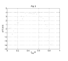
- Fig. 3 is a diagram of receiver sensitivity improvement versus modulation rate for a typical transmission link consisting of five fiber spans of 100 km each, and
- Fig. 4 is a diagram, in which receiver sensitivity improvement versus modulation depth is plotted for a typical transmission link consisting of five fiber spans of 100 km each.
- In Fig. 1, there is shown an
apparatus 10 for transmitting an optical signal that includes a number of optical transmitters Tx1...n, awavelength multiplexer 12, aphase modulator 13 and anamplifier 14. Each optical transmitter Tx1...n is clocked by a specific clock signal c1...n and it generates an optical signal, which is modulated by an electrical data signal d1...n at bit rate R1...n, to be transmitted on a specific channel in a wavelength-division multiplexing (WDM) transmission system. Each transmitter is connected to an input port of themultiplexer 12, in which all connected signals are combined into one single multiplexed signal to be transmitted on oneoptical fiber 15. The multiplexed signal is then phase modulated by aphase modulator 13, which operates at a frequency fPM and is coupled to the output port of the wavelength multiplexer and to the input port of thebooster amplifier 14. - Further, in Fig. 1, there is shown an
apparatus 16 for receiving an optical signal. Theapparatus 16 comprises anamplifier 17, ademultiplexer 18 and a number of optical receivers Rx1...n for receiving and converting the optical signals to electrical signals. - Referring to Fig. 1, the
phase modulator 13 modulates the phase of the multiplexed optical signal. The modulation is controlled by means of an electrical wave having a peak-to-peak amplitude V and a frequency fPM such that the peak-to-peak amplitude of the phase modulation is ΔΦpp = Π V / VΠ (i.e. ΔΦpp = Π, if V = VΠ) and its frequency becomes fPM. The electrical wave controlling the phase modulator is independent of the clock signals c1...n employed for generating each respective signal. As a consequence, the phase modulation is asynchronous for each channel. It is preferred that the waveform of the modulation signal is periodical and has an inclined leading edge and an inclined trailing edge. Most preferably, a sinusoidal waveform is employed. In the following discussion a sinusoidal wave is employed, but it is to be understood that other non-square waves alternatively may be used. If the phase-modulating signal has the form of a sine wave, the optical phase Φ(t) of the modulation signal and its time derivative ν(t) = (1/2π) dΦ/dt (i.e. its frequency shift) will for each wavelength channel be:

- According to the equations above, neighboring bit slots (see Fig. 2) will have different phase and different frequency shifts. If the phase modulation is synchronous, the phase and frequency shift (at the bit-slot center) would alternate between N values, where the integer N = R / fPM and R denotes the bit rate. For example, if N = 2, phase and frequency shift would alternate between two values. The amplitude of this phase alternation and frequency-shift alternation would be constant throughout the signal. In the case of asynchronous phase modulation, this will be true only for bit slots close to each other, and only if the ratio between the bit rate and the phase-modulation frequency is approximately equal to N.
- Referring to Fig. 2, there is illustrated how the phase and frequency shift vary for different pulses, or bit slots. In the Figure the centers of four pulses (bit slot centers) denoted by k, k+1, h and h+1, are indicated by means of dashed lines.
- In the topmost diagram of Fig. 2, there is shown the intensity of a number of pulses of an optical signal at bit rate R. For the sake of simplicity, all the pulses correspond to logical "ones".
- In the bottommost diagram of Fig. 2, there is illustrated the phase of the signal after being phase-modulated at a frequency fPM approximately half the bit rate R of the signal. It can be seen that, for bit slot k, the optical phase is maximal (i.e. the bit slot center coincides with the maximum of the modulation signal). For bit slot k+1, the phase is minimal (i.e. the bit slot center coincides with the minimum of the modulation signal): the phase-alternation amplitude is maximum, ΔΦk = ΔΦpp. The frequency shift is zero for both bit slots k and k+1: the amplitude of the frequency-shift alternation is zero, Δνk = 0
- The difference between fPM and R will cause a progressive shift in the pulses illustrated in the topmost diagram in Fig. 2, so that away from bit slot k, the amplitude of the phase alternation and frequency-shift alternation will be different than ΔΦk and Δνk.
- Moving to the right in the topmost diagram of Fig. 2, around a bit slot h far enough from bit slot k, a condition is reached in which the bit slot center coincides with the zero-crossing point of the modulation signal, so that the phase-alternation amplitude is zero, ΔΦk = 0, and the amplitude of the frequency-shift alternation is maximum, Δνk = ΔΦpp fPM.
- In other words, because the phase modulation and the data signal are asynchronous, phase alternation of the resulting phase-modulated signals will for N = 2 vary with time, continuously oscillating between two conditions, as illustrated in Fig. 2:
- A) a first condition prevails e.g. for bits k and k+1 in Fig. 2, wherein the phase-modulation maxima and minima coincide with the bit slot centers, so that ΔΦk = ΔΦ and Δνk = 0.
- B) a second condition prevails e.g. for bits h and h+1 in Fig. 2, wherein the phase-modulation zero-crossing points coincide with the bit slot centers, so that ΔΦh = 0 and Δνh = ΔΦpp fPM.
- In condition A, the build-up of ghost pulses and amplitude jitter is reduced because of alternating phase (as in APRZ). In prior art, it has been shown that reduction of intra-channel non-linear effects is achieved for phase-alternation amplitude ΔΦ =
Π 2 for very narrow pulses and slightly higher values of ΔΦ for wider pulses. In condition B, the build-up of ghost pulses and amplitude jitter is reduced because the alternating frequency shift fulfills a frequency matching condition for reduction of intra-channel non-linear distortion. In this case, reduction of distortion due to non-linear intra-channel effects increases with increasing Δν. During the transitions between extreme conditions A and B, the bit slots will at least partially undergo the phase and frequency alternations described in the above, which will result in increased non-linear tolerance for the channel. - For N > 2, phase and frequency shift will vary between several values (instead of two as for N = 2), and for non-integer N the phase and frequency shift will no longer vary periodically, but the neighboring bit slots will still have different values of phase and frequency shift. For fPM ≈ 0.5 R, further improved receiver sensitivity is obtained at approximately ΔΦpp = Π / 2, (even considering that for most of the time the bit alternation is ΔΦ < ΔΦpp).
- When it comes to the other phase modulation parameter, fPM, this should be high enough to have significant frequency-match break-up, but also not large enough to cause such a severe spectral broadening that neighboring wavelength channels start interfering with each-other. As a first approximation, the spectral broadening is determined by the shifting of spectral components away from each other by an amount corresponding to the frequency-shift alternation, ΔΦpp fPM. If this shift exceeds the spectral range allocated to half the channel spacing, i.e. the channel spacing, Sch, a part of the spectrum will end up in the wavelength region allocated to the neighboring channel, and interference will take place. Therefore the following condition should be met: ΔΦpp fPM < Sch, or fPM < Sch/ΔΦpp.
- As an example of how the proper choice of ΔΦpp and fPM can improve the performance of a transmission link, numerical simulations were performed for a dispersion-managed system, consisting of 5 spans, each 100 km long, with perfect on-line dispersion compensation and no pre-compensation. The system was set up with three channels of RZ signals with 50% duty cycle at R = 40 Gb/s, and channel spacing was 100 GHz. The wavelength multiplexer has a 3-dB pass band of 75 Ghz band and the wavelength demultiplexer has a 3-dB pass band of 50 GHz. The system was set up with 6 dBm launch power per channel into the SSMF (standard single-mode fiber), and 1 dBm into the DCF (dispersion compensating fiber). The transmission performance is evaluated in terms of power penalty, i.e. degradation in receiver sensitivity with respect to the sensitivity is obtained for a transmitter and a receiver with no transmission line therebetween. Receiver sensitivity is defined as the minimum power needed at the receiver in order to achieve a bit error ratio of 10-9.
- The results of the simulations for the central wavelength channel, are plotted in Fig. 3 and 4. It can be seen that asynchronous phase modulation improves the non-linear tolerance in a approximate range of 0 < ΔΦ < Sch / fPM. Performance improvement is very high for values of ΔΦpp,opt around 2 Π / 3, and fPM,opt around 0.5 R, and slightly lower but still high within a range of ±40% from ΔΦpp,opt and fPM,opt. The values ΔΦpp,opt and fPM,opt will most likely change if the parameters of the optical system, such as pulse chirp, duty cycle, span length, dispersion map and launch power, are changed.
- In the diagram in Fig. 3, receiver sensitivity improvement in dB, ΔRS, as a function of phase modulation rate over bit rate is plotted, for ΔΦpp = 5 Π / 6. As can be seen from Fig. 3, a phase-modulation frequency up to 80% of the bit rate (that is in this case of a frequency of 10-30 GHz for a 40 Gb/s signal) improves the transmission performance.
- For the phase-modulation amplitude of ΔΦPP = 5 Π / 6, it is preferred to set (or adjust) the modulation rate in a range from approximately 20% to 70% of the bit rate of the any one the three channels, whereby the receiver sensitivity improvement becomes greater than or equal to 1.5 dB. Most preferably, the modulation rate is set (or is adjustable) in a range from approximately 35% to 65%, whereby the receiver sensitivity becomes greater than or equal to 3 dB.
- Fig. 4 shows a further result from a simulation, wherein the modulation depth is varied for three different phase-modulation frequencies: 24%, 49% and 73% of the bit rate R. In Fig. 4, receiver sensitivity improvement as a function of modulation depth over Π is plotted. In general, there is an improvement of the signal quality, when the modulation depth is less than channel spacing divided by the modulation rate. It is, however, preferred to have a receiver sensitivity improvement of 1.5 dB or more, which results in a modulation depth of approximately 2 Π / 3 ± 40 % for a modulation rate in the vicinity of half the bit rate, which is approximately equal to a range of 0.4 Π - Π. From the Fig. 4, it can also be noted that for a range of 0.5 Π - 0.9 Π, the receiver sensitivity is above approximately 3 dB.
- Even though the invention has been described with reference to a specific exemplifying embodiment thereof, many different alterations, modifications and the like will become apparent for those skilled in the art. The described embodiment is therefore not intended to limit the scope of the invention, as defined by the appended claims.
Claims (14)
- A method for modulating the phase of a plurality of wavelength channels spaced from each other by a channel spacing in a WDM-transmission link, comprising the step of:asynchronously modulating said plurality of channels, whereina modulation rate of said modulation is set to a value in a range from approximately 20% to approximately 70% of a bit rate of any one of the channels, anda modulation depth of said modulation is set to a value in a range from zero to approximately said channel spacing divided by said modulation rate.
- The method according to claim 1, wherein said modulation depth is set to a value in a range of approximately 0.4 Π - Π.
- The method according to claim 1, wherein said modulation depth is set to a value in a range of approximately 0.5 Π - 0.9 Π.
- The method according to any one of the preceding claims, wherein said modulation rate is set to a value in a range from approximately 35% to approximately 65% of said bit rate.
- The method according to any one of the preceding claims, wherein said plurality of channels comprise RZ-type signals.
- The method according to any one of the preceding claims, wherein a modulation signal employed in the asynchronous modulation is arranged to have an inclined leading edge and an inclined trailing edge.
- The method according to claim 6, wherein the modulation signal has a sinusoidal waveform.
- The method according to any one of the preceding claims, further comprising a step of multiplexing said plurality of channels into said WDM-transmission link prior to said asynchronous modulation.
- An optical transmitter for use in an optical transmission network, comprising:a plurality of sources for generating modulated optical signals, each source representing a channel in a WDM-transmission link, wherein channels are spaced from each other by a channel spacing,a multiplexer connected to each of said sources for receiving said modulated optical signals and transmitting said modulated optical signals over said transmission link,a phase modulator arranged to modulate the phase of said modulated optical signals, andan optical amplifier for amplifying said modulated optical signals, whereina modulation rate of said phase modulator is set to a value in a range from approximately 20% to approximately 70% of a bit rate of any one of the modulated optical signals, anda modulation depth of said phase modulator is set to a value in a range from zero to approximately said channel spacing divided by said modulation rate.
- The optical transmitter according to claim 9, wherein said modulation depth is set to a value in a range of approximately 0.4 Π - Π.
- The optical transmitter according to claim 9 or 10, wherein said modulation depth is set to a value in a range of approximately 0.5 Π - 0.9 Π.
- The optical transmitter according to any one of claims 9-11, wherein said modulation rate is set to a value in a range from approximately 35% to approximately 65% of said bit rate.
- The optical transmitter according to any one of claims 10-12, wherein said modulated optical signals are RZ-type signals.
- The optical transmitter according to any one of claims 9-13, wherein said phase modulator is located after the multiplexer such that all channels are modulated simultaneously.
Priority Applications (1)
| Application Number | Priority Date | Filing Date | Title |
|---|---|---|---|
| EP06112780A EP1848129A1 (en) | 2006-04-19 | 2006-04-19 | Multi-channel phase modulation method for suppression of intra-channel non-linear distortion |
Applications Claiming Priority (1)
| Application Number | Priority Date | Filing Date | Title |
|---|---|---|---|
| EP06112780A EP1848129A1 (en) | 2006-04-19 | 2006-04-19 | Multi-channel phase modulation method for suppression of intra-channel non-linear distortion |
Publications (1)
| Publication Number | Publication Date |
|---|---|
| EP1848129A1 true EP1848129A1 (en) | 2007-10-24 |
Family
ID=36933560
Family Applications (1)
| Application Number | Title | Priority Date | Filing Date |
|---|---|---|---|
| EP06112780A Withdrawn EP1848129A1 (en) | 2006-04-19 | 2006-04-19 | Multi-channel phase modulation method for suppression of intra-channel non-linear distortion |
Country Status (1)
| Country | Link |
|---|---|
| EP (1) | EP1848129A1 (en) |
Cited By (1)
| Publication number | Priority date | Publication date | Assignee | Title |
|---|---|---|---|---|
| US9331791B2 (en) | 2014-01-21 | 2016-05-03 | Nano Retina Ltd. | Transfer of power and data |
Citations (2)
| Publication number | Priority date | Publication date | Assignee | Title |
|---|---|---|---|---|
| US6606178B1 (en) * | 1999-09-23 | 2003-08-12 | Corning Incorporated | Method and system to reduce FWM penalty in NRZ WDM systems |
| US20040057734A1 (en) * | 2002-09-25 | 2004-03-25 | Lucent Technologies, Inc. | Method and system for reducing transmission penalties associated with ghost pulses |
-
2006
- 2006-04-19 EP EP06112780A patent/EP1848129A1/en not_active Withdrawn
Patent Citations (2)
| Publication number | Priority date | Publication date | Assignee | Title |
|---|---|---|---|---|
| US6606178B1 (en) * | 1999-09-23 | 2003-08-12 | Corning Incorporated | Method and system to reduce FWM penalty in NRZ WDM systems |
| US20040057734A1 (en) * | 2002-09-25 | 2004-03-25 | Lucent Technologies, Inc. | Method and system for reducing transmission penalties associated with ghost pulses |
Non-Patent Citations (2)
| Title |
|---|
| FORZATI M ET AL: "REDUCTION OF INTRACHANNEL FOUR-WAVE MIXING USING THE ALTERNATE PHASE RZ MODULATION FORMAT", IEEE PHOTONICS TECHNOLOGY LETTERS, vol. 14, no. 9, 1 September 2002 (2002-09-01), pages 1285 - 1287, XP002397973 * |
| RHEE J-K ED - SOCIETE DES ELECTRICIENS ET DES ELETRONICIENS: "FOUR WAVE MIXING SUPPRESSION USING PHASE MODULATION IN MULTI-SPAN DWDM TRANSMISSIONS", 25TH EUROPEAN CONFERENCE ON OPTICAL COMMUNICATION. (ECOC'99). NICE, FRANCE, SEPT. 27 - 30, 1999. REGULAR AND INVITED PAPERS, EUROPEAN CONFERENCE ON OPTICAL COMMUNICATION (ECOC), PARIS : SEE, FR, vol. VOL. I OF II, 26 September 1999 (1999-09-26), pages I - 206, XP001035365, ISBN: 2-912328-12-8 * |
Cited By (1)
| Publication number | Priority date | Publication date | Assignee | Title |
|---|---|---|---|---|
| US9331791B2 (en) | 2014-01-21 | 2016-05-03 | Nano Retina Ltd. | Transfer of power and data |
Similar Documents
| Publication | Publication Date | Title |
|---|---|---|
| US7512338B2 (en) | Method and apparatus for pulse generation and adaptive pulse generation for optical communications | |
| US5946119A (en) | Wavelength division multiplexed system employing optimal channel modulation | |
| EP1624595A1 (en) | Transmission of optical signals of different modulation formats in discrete wavelength bands | |
| US7373040B2 (en) | Optical transmission system including dispersion slope compensation | |
| EP1204228B1 (en) | Optical modulation scheme for NRZ signals and optical transmitter | |
| EP1953933B1 (en) | Transmission system and transmission method | |
| US7796897B2 (en) | WDM optical transmission system and WDM optical transmission method | |
| JP2003510890A (en) | Method and system for reducing FWM loss in NRZWDM systems | |
| JP4320573B2 (en) | Optical receiving method, optical receiving apparatus and optical transmission system using the same | |
| US8213798B2 (en) | Optical transmission apparatus, wavelength division multiplexing optical communication system and optical transmission method | |
| US6014479A (en) | High channel density wavelength division multiplex (WDM) optical transmission system and method with negligible four-wave mixing (FWM) penalty | |
| US7305189B2 (en) | Phase modulation for an optical transmission system | |
| US7260332B1 (en) | Asynchronous chirped systems, apparatuses, and methods | |
| EP1848129A1 (en) | Multi-channel phase modulation method for suppression of intra-channel non-linear distortion | |
| US7319823B2 (en) | Modulation scheme and transmission system for NRZ signals with left and right side filtering | |
| JP3523998B2 (en) | Optical transmission system | |
| EP1355435B1 (en) | Phase modulation for an optical transmission system | |
| JP2005094287A (en) | Optical transmission and reception method and system, and optical transmission method and apparatus | |
| US20050041983A1 (en) | Method of forming a coded optical signal with a return to zero or non return to zero format |
Legal Events
| Date | Code | Title | Description |
|---|---|---|---|
| PUAI | Public reference made under article 153(3) epc to a published international application that has entered the european phase |
Free format text: ORIGINAL CODE: 0009012 |
|
| STAA | Information on the status of an ep patent application or granted ep patent |
Free format text: STATUS: THE APPLICATION HAS BEEN PUBLISHED |
|
| AK | Designated contracting states |
Kind code of ref document: A1 Designated state(s): AT BE BG CH CY CZ DE DK EE ES FI FR GB GR HU IE IS IT LI LT LU LV MC NL PL PT RO SE SI SK TR |
|
| AX | Request for extension of the european patent |
Extension state: AL BA HR MK YU |
|
| AKX | Designation fees paid | ||
| REG | Reference to a national code |
Ref country code: DE Ref legal event code: 8566 |
|
| STAA | Information on the status of an ep patent application or granted ep patent |
Free format text: STATUS: THE APPLICATION IS DEEMED TO BE WITHDRAWN |
|
| 18D | Application deemed to be withdrawn |
Effective date: 20080425 |