EP1845542A1 - Multistage switch - Google Patents
Multistage switch Download PDFInfo
- Publication number
- EP1845542A1 EP1845542A1 EP06711763A EP06711763A EP1845542A1 EP 1845542 A1 EP1845542 A1 EP 1845542A1 EP 06711763 A EP06711763 A EP 06711763A EP 06711763 A EP06711763 A EP 06711763A EP 1845542 A1 EP1845542 A1 EP 1845542A1
- Authority
- EP
- European Patent Office
- Prior art keywords
- magnetoelectric
- magnetoelectric transducer
- magnetic sensor
- push button
- switch
- Prior art date
- Legal status (The legal status is an assumption and is not a legal conclusion. Google has not performed a legal analysis and makes no representation as to the accuracy of the status listed.)
- Granted
Links
Images
Classifications
-
- G—PHYSICS
- G03—PHOTOGRAPHY; CINEMATOGRAPHY; ANALOGOUS TECHNIQUES USING WAVES OTHER THAN OPTICAL WAVES; ELECTROGRAPHY; HOLOGRAPHY
- G03B—APPARATUS OR ARRANGEMENTS FOR TAKING PHOTOGRAPHS OR FOR PROJECTING OR VIEWING THEM; APPARATUS OR ARRANGEMENTS EMPLOYING ANALOGOUS TECHNIQUES USING WAVES OTHER THAN OPTICAL WAVES; ACCESSORIES THEREFOR
- G03B9/00—Exposure-making shutters; Diaphragms
- G03B9/08—Shutters
-
- H—ELECTRICITY
- H03—ELECTRONIC CIRCUITRY
- H03K—PULSE TECHNIQUE
- H03K17/00—Electronic switching or gating, i.e. not by contact-making and –breaking
- H03K17/94—Electronic switching or gating, i.e. not by contact-making and –breaking characterised by the way in which the control signals are generated
- H03K17/965—Switches controlled by moving an element forming part of the switch
- H03K17/97—Switches controlled by moving an element forming part of the switch using a magnetic movable element
-
- H—ELECTRICITY
- H03—ELECTRONIC CIRCUITRY
- H03K—PULSE TECHNIQUE
- H03K17/00—Electronic switching or gating, i.e. not by contact-making and –breaking
- H03K17/94—Electronic switching or gating, i.e. not by contact-making and –breaking characterised by the way in which the control signals are generated
- H03K17/965—Switches controlled by moving an element forming part of the switch
- H03K17/97—Switches controlled by moving an element forming part of the switch using a magnetic movable element
- H03K2017/9713—Multiposition, e.g. involving comparison with different thresholds
Definitions
- the present invention relates to multistage switches. More specifically, the present invention relates to a multistage switch used for a shutter switch of a camera, a photographing switch of a video camera, a switch of other electronic apparatuses, etc., for providing a single switch with a plurality of operation instruction functions.
- multistage switches using disc springs have been generally known (see Patent Document 1).
- the multistage switches using disc springs function as multistage switches in which a switch push button is pressed by a user so that a plurality of disc springs provided in a multistage switch are sequentially deformed according to pressing force with which the disc springs are pressed and the operating state of an electronic apparatus is sequentially switched.
- the multistage switches of the related art using disc springs, etc. allow the operating state to be switched according to an amount by which a switch push button is pressed during the operation of the multistage switch. If a user desires to switch to the operating state of the first stage, he/she may apply large force to the switch push button against the elastic force of the disc springs to switch to the operating state of the second or further stage at a time. Thus, the user who wishes to obtain a desired operating state may not successfully obtain the desired operating state due to the mismatch between the user's feeling of operation and the actual operation of the multistage switch.
- a multistage switch used for a shutter of a camera typically has two operating stages, the first stage corresponding to the focusing operation and the second stage corresponding to the shutter release operation, i.e., the photographing operation. If the user fails to accurately press the switch push button, the shutter may often be released in an out-of-focus state.
- the present invention provides a multistage switch including a magnetic sensor including a substrate and a magnetoelectric transducer defined on the substrate; a switch push button; and a magnetic member provided in the switch push button and disposed so as to face the magnetoelectric transducer, wherein the magnetic sensor detects, as a detected potential, a potential produced at the magnetoelectric transducer in the magnetic sensor by a shift in a distance between the magnetic sensor and the magnetic member, at least two threshold values are provided for the detected potential, and an operating state is changed according to results of comparison between the threshold values and the detected potential.
- the magnetoelectric transducer is a semiconductor magnetoresistive element.
- the magnetic sensor includes two magnetoelectric transducers connected in series.
- the detected potential is a detected potential at a node between the two magnetoelectric transducers.
- a first magnetoelectric transducer of the two magnetoelectric transducers has a predetermined shift in a potential produced by a shift in a distance between the first magnetoelectric transducer and the magnetic member, and a second magnetoelectric transducer of the two magnetoelectric transducers has substantially no shift in a potential produced by a shift in a distance between the second magnetoelectric transducer and the magnetic member.
- the first magnetoelectric transducer and the second magnetoelectric transducer have substantially identical temperature characteristics.
- the two magnetoelectric transducers are semiconductor magnetoresistive elements.
- the first magnetoelectric transducer includes a semiconductor magnetoresistive thin film defined on a substrate, a plurality of short-circuiting electrodes defined on the semiconductor magnetoresistive thin film, and an external electrode connected to the outside.
- the second magnetoelectric transducer includes a semiconductor magnetoresistive thin film defined on the substrate, and an external electrode connected to the outside, and includes on the semiconductor magnetoresistive thin film no short-circuiting electrodes or a smaller number of short-circuiting electrodes than the number of short-circuiting electrodes defined in the first magnetoelectric transducer.
- a moving mechanism of the switch push button is independent from an operation signal system in the magnetic sensor.
- the magnetic sensor includes a package covering the magnetoelectric transducer, and the package is disposed on the magnetic sensor so that a spacing between the package and a magnetosensitive section of the magnetoelectric transducer is set to be not more than 0.3 mm.
- the magnetic member and the magnetoelectric transducer are used to detect, as a potential, a change in magnetic force due to a shift in the distance therebetween, and a user can smoothly press a switch push button without being subjected to strong physical reaction force such as force of disc springs. Therefore, for example, when the multistage switch is used in a camera or the like, the user does not feel strong reaction force, and can perform the focusing operation corresponding to the operating state of the first stage with a low possibility of causing camera-shake, etc.
- the multistage switch used in any other compact electronic apparatus can also provide stable operation characteristics.
- a semiconductor magnetoresistive element is used as a magnetoelectric transducer, even if the moving distance of the switch push button is small, that is, if the change in the distance between the magnetic member and the semiconductor magnetoresistive element is small, an output characteristic having a large output value with respect to a small change in magnetic force caused by the change in the distance can be obtained. Further, the output characteristic exhibits a sharp linearity, and it is easy to set threshed values for multiple stages.
- the magnetic sensor includes two magnetoelectric transducers connected in series, of which a second magnetoelectric transducer has substantially no magnetic sensitivity. Therefore, a shift in a detected potential, which is a potential at a node between the two magnetoelectric transducers, depends on electrical characteristics of a first magnetoelectric transducer. Since the temperature characteristics of the two magnetoelectric transducers connected in series are substantially identical, no potential difference between the two magnetoelectric transducers occurs due to the temperature change. Thus, the detected potential at the node between the two magnetoelectric transducers is not affected by the temperature change.
- the detected potential of the magnetic sensor in the present embodiment is therefore a potential indicating a shift that purely depends on the magnetic change, in which the influence of a change in ambient temperature is canceled, in the shift in the potential of the first magnetoelectric transducer.
- the semiconductor magnetoresistive element serving as the first magnetoelectric transducer includes a predetermined number of short-circuiting electrodes to achieve a predetermined magnetoresistive effect
- the second semiconductor magnetoresistive element includes no short-circuiting electrodes or a smaller number of short-circuiting electrodes to substantially eliminate the magnetoresistive effect.
- an operating mechanism of the switch push button and an operation signal system of the magnetic sensor are independent, that is, the operation signal system is separated, thus providing the switch push button with an operation that is not related to an operation signal of the magnetic sensor.
- the switch push button can be moved between threshold values irrespective of an operation signal system, thus preventing the user from excessively pressing the switch push button when moving the switch push button between the threshold values. Such malfunction can be prevented.
- a package is disposed on the magnetic sensor so that a spacing between the package and the magnetoelectric transducers is set to be not more than 0.3 mm, thus achieving a reduction in thickness of the magnetic sensor. This ensures a wide operation area including the switch push button.
- a multistage switch according to an embodiment of the present invention will be described with reference to Figs. 1 and 2.
- the embodiment will be described in the context of a multistage switch used for a shutter of a camera by way of example.
- a multistage switch 10 shown in Fig. 1 includes a switch push button 11 serving as a shutter release button.
- the switch push button 11 is surrounded by a housing 12 of the camera, and is generally projected slightly from the housing.
- a magnet 13 serving as a magnetic member is disposed in a recess of the inner wall surface of the switch push button 11.
- the magnet 13 is disposed so that lines of magnetic force are generated in the direction in which the switch push button 11 is pressed, i.e., in the direction indicated by an arrow shown in Fig. 1.
- the south pole of the magnet 13 is oriented toward the top of the switch push button 11, and the north pole of the magnet 13 is oriented on the bottom side of the switch push button.
- the multistage switch 10 further includes a magnetic sensor 14.
- the magnetic sensor 14 includes a substrate 15 defining a main circuit of the sensor.
- the substrate 15 is made of, for example, a glass epoxy material or ceramic material.
- Two magnetoelectric transducers 21 and 31 are mounted on a surface of the substrate 15. These two magnetoelectric transducers 21 and 31 are disposed so as to face the north pole of the magnet 13.
- weak reaction force is only required to return the switch push button 11 to the initial position, and a weak spring, a low-repulsive material, or the like can be provided between the switch push button 11 and the substrate 15.
- a low-repulsive material 16 is used.
- the two magnetoelectric transducers 21 and 31 include bases 22 and 32, respectively, and the bases 22 and 32 have magnetosensitive sections 23 and 33 and external electrodes (not shown in Fig. 1), respectively.
- the two magnetoelectric transducers 21 and 31 are mounted using flip-chip bonding so that the surfaces on which the magnetosensitive sections 23 and 33 are defined face the substrate 15.
- the magnetoelectric transducers 21 and 31 are mounted using the external electrodes through an electroconductive adhesive 17.
- Fig. 2 shows two semiconductor magnetoresistive elements used as the two magnetoelectric transducers 21 and 31 according to the embodiment of the present invention.
- the two magnetoelectric transducers 21 and 31 share one base made of silicone into which the bases 22 and 32 are unified.
- a semiconductor magnetoresistive thin film 23a made of InSb (indium antimonide) is defined in a meandering line pattern.
- the semiconductor magnetoresistive thin film 23a is generally formed using vacuum deposition.
- a plurality of multi-layered short-circuiting electrodes 23b made of Ni/Cr/Au, Cr/Ni/Au, or the like are defined on the semiconductor magnetoresistive thin film 23a.
- the short-circuiting electrodes 23b are formed into a multi-layer structure using a method such as vapor deposition or sputtering. In Fig. 2, however, the multi-layer structure is not shown for simplification of illustration.
- the semiconductor magnetoresistive thin film 23a and the short-circuiting electrodes 23b function as the magnetosensitive section 23.
- the first magnetoelectric transducer 21 further includes an external electrode 24 to be connected to a circuit pattern on the substrate 15 or the second magnetoelectric transducer 31.
- the external electrode 24 is formed of the same electrode material using the same method as the short-circuiting electrodes 23b.
- a semiconductor magnetoresistive thin film 33a made of InSb (indium antimonide) is defined in a meandering line pattern.
- the semiconductor magnetoresistive thin film 33a is formed in the same shape, of the same electrode material, and using the same method as the semiconductor magnetoresistive thin film 23a of the first magnetoelectric transducer 21.
- a plurality of multi-layered short-circuiting electrodes 33b are defined on the semiconductor magnetoresistive thin film 33a. The number of defined short-circuiting electrodes 33b is smaller than the number of short-circuiting electrodes 23b defined on the first magnetoelectric transducer 21.
- the semiconductor magnetoresistive thin film 33a and the short-circuiting electrodes 33b function as the magnetosensitive section 33.
- the second magnetoelectric transducer 31 further includes an external electrode 34 to be connected to the circuit pattern of the substrate 15 or the first magnetoelectric transducer 21.
- the first and second magnetoelectric transducers 21 and 31 having the above-described structure have largely different magnetic resistance change characteristics. Specifically, the first magnetoelectric transducer 21 has a predetermined magnetic resistance change characteristic while substantially no magnetic resistance change occurs in the second magnetoelectric transducer 31. However, the first and second magnetoelectric transducers 21 and 31 exhibit substantially identical resistance changes due to the temperature change.
- the two magnetoelectric transducers 21 and 31 are connected in series, and an input voltage Vin is applied. If the multistage switch 10 has two operating stages to be switched, first and second threshold values V1 and V2 are set in the magnetic sensor 14.
- a voltage V at a node between the two magnetoelectric transducers 21 and 31 is compared, as a detected potential of the magnetic sensor 14, with the first threshold value V1 using a comparator C1, and is also compared with the second threshold value V2 using a comparator C2.
- An operation instruction is transmitted from the magnetic sensor 14 to the camera according to those comparison results.
- the multistage switch has n operating stages to be switched, as indicated by a two-dot chain line shown in Fig. 4, a circuit structure in which the voltage V is compared with the n-th threshold Vn using a comparator Cn may be used.
- the pressed switch push button 11 gradually approaches the magnetic sensor 14. Therefore, the magnet 13 in the switch push button approaches the first and second magnetoelectric transducers 21 and 31 in the magnetic sensor 14. Then, the resistance value of the first magnetoelectric transducer 21 changes.
- the resistance value of the second magnetoelectric transducer 31 does not substantially change.
- the change in resistance value due to the approaching of the magnet 13 causes a change in the voltage V at the node between the two magnetoelectric transducers 21 and 31, and the voltage V is compared with the first threshold value V1, the second threshold value V2, ..., and the n-th threshold value Vn.
- An operation instruction is transmitted from the magnetic sensor 14 to the camera according to those comparison results.
- the resistance change characteristic of the second magnetoelectric transducer 31 due to the temperature change is substantially identical to that of the first magnetoelectric transducer 21. Therefore, the potential V at the node between the two magnetoelectric transducers 21 and 31 depends on electrical characteristics of the first magnetoelectric transducer 21, i.e., the magnetic sensitivity. Since the temperature characteristics of the two magnetoelectric transducers 21 and 31 connected in series are substantially identical, no potential difference between the two magnetoelectric transducers 21 and 31 occurs due to the temperature change. Thus, the voltage V serving as a detected potential at the node between the two magnetoelectric transducers 21 and 31 is not affected by the temperature change.
- the voltage V serving as a detected potential of the magnetic sensor 14 of the present embodiment is therefore a potential indicating a shift that purely depends on the magnetic change, in which the influence of a change in ambient temperature is canceled, in the shift in the potential of the first magnetoelectric transducer 21.
- the distance between the magnet 13 and the two magnetoelectric transducers 21 and 31 is set to 2 mm when the switch push button 11 is not pressed.
- the voltage V at the node between the magnetoelectric transducers 21 and 31 in this state is set to 2.6 V. It is assumed that the switch push button 11 can be pressed up to 1.7 mm.
- the relationship between the pressing amount of the switch push button and the voltage V at the node between the magnetoelectric transducers 21 and 31 is that although a large change does not occur in the voltage V when the pressing amount is 0 to about 0.5 mm, a significant change gradually occurs in the voltage V with respect to the pressing amount.
- the pressing amount is 0.8 mm or more, it can be found that the voltage V changes in a substantially one-dimensional linear manner.
- the output signal can be directly compared with the threshed values for determining the operation of the multistage switch 10. Further, the voltage V to be output permits a conversion efficiency of about 10% of the input voltage Vin applied to the two magnetoelectric transducers connected in series, and higher efficiency than various magnetoelectric transducers such as Hall elements and magnetoresistive elements formed of ferromagnetic metal thin films is attained, which is suitable for use in compact electronic apparatuses.
- the first threshold value V1 is set to 2.7 V ⁇ 0.05 V and the second threshold value V2 is set to be not less than 2.9 V to ensure a difference of 0.4 mm in the pressing amount of the switch push button 11 from the first threshold value V1 to the second threshold value V2.
- a voltage value serving as a threshold value may be set as a range, like the first threshold value V1, or may be set as a boundary, like the second threshold value V2, e.g., whether or not the voltage value exceeds 2.9 V.
- the first threshold value V1 is used for focusing and is given a certain range.
- the second threshold value V2 is not given a specific range and is set so that the operation is performed if the voltage V exceeds the second threshold value V2. Even if the first threshold value V1 is used for the focusing operation, the first threshold value V1 may not be given a range and may be set to, for example, 2.7 V so that the focusing operation can be performed if the voltage V exceeds the threshold value of 2.7 V.
- the voltage V serving as a detected potential linearly changes, it is easy to set a threshed value for the multistage switch. Further, the number of stages can be increased only with a simple circuit design. Therefore, multiple stages more than two stages can easily be set, which is substantially impossible in a multistage sensor using disc springs as described in the related art.
- a semiconductor magnetoresistive element is used as a magnetoelectric transducer.
- a Hall element or a ferromagnetic magnetoresistive element can be used because similar advantages are achieved without generating strong reaction force when the switch push button is pressed.
- the conversion efficiency of a Hall element or a ferromagnetic magnetoresistive element with respect to an input voltage is lower than that of a semiconductor magnetoresistive element. Therefore, preferably, a semiconductor magnetoresistive element is used as a magnetoelectric transducer in a multistage switch of a compact electronic apparatus.
- a switch push button and a magnet are separately provided by way of example.
- a switch push button formed by combining a magnetic member having magnetic properties with a switch push button into a single unit e.g., a switch push button made of plastic magnet, may be used.
- a semiconductor magnetoresistive element is used as a magnetoelectric transducer and is mounted on a substrate using flip-chip bonding by way of example.
- a magnetosensitive section may be mounted using wire bonding so as to face a magnetic member.
- two magnetoelectric transducers are used, of which the second magnetoelectric transducer has a lower magnetic sensitivity and is used as a magnetoelectric transducer for temperature compensation.
- the second magnetoelectric transducer may be mounted on a corner of a substrate and disposed at a position that is not affected by magnetic force.
- the second magnetoelectric transducer can be the same as the first magnetoelectric transducer, and can also be used for temperature compensation.
- the structure of the present invention in which the magnetic sensitivity of the second magnetoelectric transducer is reduced and the first and second magnetoelectric transducers are disposed adjacent to each other is suitable for use in compact electronic apparatuses.
- the operation mechanism of the switch push button has been described in the context of a weak spring or a low-repulsive material, the operation mechanism is not limited thereto. Not only a physical operation mechanism but also an operation mechanism that is controlled by an electrical signal can be used as far as the operation mechanism of the switch push button is independent from an operation signal system of the magnetic sensor, that is, an operation mechanism that is not related to an operation signal of the magnetic sensor.
- the magnetic sensor is not provided with a package.
- the magnetic sensor 14 may be configured such that the magnetoelectric transducers 21 and 31 are covered by a package 18.
- the magnetoelectric transducers 21 and 31 are mounted using wire bonding so that the magnetosensitive sections 23 and 33 face the magnetic member and the bases 22 and 32 are mounted on the substrate 15.
- wires are not shown. In general, wires formed of gold or aluminum wires having a line diameter of 50 ⁇ m are used, and ball bonding or wedge bending is performed.
- a resin with flexibility is coated about 0.1 mm thick on the surface of the magnetoelectric transducers so that no stress is applied to loop (slack) portions or bonding portions of the wires. Then, the magnetoelectric transducers are packaged with a high-fluidity resin.
- the thickness of the resin used for packaging is reduced as much as possible to increase the used range of the output characteristic. However, if the thickness is too thin, the physical strength of the elements is reduced. Therefore, preferably, the package thickness is about 0.15 to 0.20 mm.
- the package design is done so that a spacing t between the package 18 and the magnetosensitive sections 23 and 33 of the magnetoelectric transducers 21 and 31 is not more than 0.3 mm, thereby reducing the thickness of the magnetic sensor to ensure a large operation region including the switch push button 11.
- a multistage switch of the present invention allows a user to smoothly press a switch push button without being subjected to strong physical reaction force such as force of disc springs. Therefore, particularly when the multistage switch is used in a camera or the like, the focusing operation corresponding to the operating state of the first stage can be performed with a low possibility of occurrence of camera-shake, etc.
- the multistage switch used in a camera can be used not only as a multistage switch used for two operations of focusing and releasing a shutter but also as a multistage switch to be operated in a larger number of stages.
- a stage for preparing the camera for the shutter release operation can be provided between the focusing stage and the actual shutter release stage, or a stage for performing photographing substantially at the same time as the actual shutter release operation, etc., can be provided. Consequently, no time error is produced between the timing of releasing a shutter in a digital camera and the timing of actually photographing a subject.
Landscapes
- Physics & Mathematics (AREA)
- General Physics & Mathematics (AREA)
- Push-Button Switches (AREA)
- Switches That Are Operated By Magnetic Or Electric Fields (AREA)
Abstract
Description
- The present invention relates to multistage switches. More specifically, the present invention relates to a multistage switch used for a shutter switch of a camera, a photographing switch of a video camera, a switch of other electronic apparatuses, etc., for providing a single switch with a plurality of operation instruction functions.
- In the related art, multistage switches using disc springs have been generally known (see Patent Document 1). The multistage switches using disc springs function as multistage switches in which a switch push button is pressed by a user so that a plurality of disc springs provided in a multistage switch are sequentially deformed according to pressing force with which the disc springs are pressed and the operating state of an electronic apparatus is sequentially switched.
- Patent Document 1:
Japanese Unexamined Patent Application Publication No. 2000-57888 - The multistage switches of the related art using disc springs, etc., allow the operating state to be switched according to an amount by which a switch push button is pressed during the operation of the multistage switch. If a user desires to switch to the operating state of the first stage, he/she may apply large force to the switch push button against the elastic force of the disc springs to switch to the operating state of the second or further stage at a time. Thus, the user who wishes to obtain a desired operating state may not successfully obtain the desired operating state due to the mismatch between the user's feeling of operation and the actual operation of the multistage switch.
- Specifically, a multistage switch used for a shutter of a camera typically has two operating stages, the first stage corresponding to the focusing operation and the second stage corresponding to the shutter release operation, i.e., the photographing operation. If the user fails to accurately press the switch push button, the shutter may often be released in an out-of-focus state.
- Recently, in particular, with the reduction in size of cameras, there has also been a demand for reduction in size of multistage switches, and a switch push button of a multistage switch is moved by a distance of approximately 2 mm from the state where no force is applied to the switch to the state where the shutter is released, i.e., the state of the second stage. The first stage corresponding to the focusing operation must be established within the distance of 2 mm. It is difficult for a general user to press the switch push button a small distance and keep the focusing operation of the first stage against the pressure of the disc springs, and camera shake may be caused. Consequently, a problem of inaccurate focusing may arise.
- To solve the foregoing problems, the present invention provides a multistage switch including a magnetic sensor including a substrate and a magnetoelectric transducer defined on the substrate; a switch push button; and a magnetic member provided in the switch push button and disposed so as to face the magnetoelectric transducer, wherein the magnetic sensor detects, as a detected potential, a potential produced at the magnetoelectric transducer in the magnetic sensor by a shift in a distance between the magnetic sensor and the magnetic member, at least two threshold values are provided for the detected potential, and an operating state is changed according to results of comparison between the threshold values and the detected potential.
- The magnetoelectric transducer is a semiconductor magnetoresistive element.
- The magnetic sensor includes two magnetoelectric transducers connected in series. The detected potential is a detected potential at a node between the two magnetoelectric transducers. A first magnetoelectric transducer of the two magnetoelectric transducers has a predetermined shift in a potential produced by a shift in a distance between the first magnetoelectric transducer and the magnetic member, and a second magnetoelectric transducer of the two magnetoelectric transducers has substantially no shift in a potential produced by a shift in a distance between the second magnetoelectric transducer and the magnetic member. The first magnetoelectric transducer and the second magnetoelectric transducer have substantially identical temperature characteristics.
- The two magnetoelectric transducers are semiconductor magnetoresistive elements. The first magnetoelectric transducer includes a semiconductor magnetoresistive thin film defined on a substrate, a plurality of short-circuiting electrodes defined on the semiconductor magnetoresistive thin film, and an external electrode connected to the outside. The second magnetoelectric transducer includes a semiconductor magnetoresistive thin film defined on the substrate, and an external electrode connected to the outside, and includes on the semiconductor magnetoresistive thin film no short-circuiting electrodes or a smaller number of short-circuiting electrodes than the number of short-circuiting electrodes defined in the first magnetoelectric transducer.
- A moving mechanism of the switch push button is independent from an operation signal system in the magnetic sensor.
- The magnetic sensor includes a package covering the magnetoelectric transducer, and the package is disposed on the magnetic sensor so that a spacing between the package and a magnetosensitive section of the magnetoelectric transducer is set to be not more than 0.3 mm.
- In the multistage switch having the above-described structure, the magnetic member and the magnetoelectric transducer are used to detect, as a potential, a change in magnetic force due to a shift in the distance therebetween, and a user can smoothly press a switch push button without being subjected to strong physical reaction force such as force of disc springs. Therefore, for example, when the multistage switch is used in a camera or the like, the user does not feel strong reaction force, and can perform the focusing operation corresponding to the operating state of the first stage with a low possibility of causing camera-shake, etc. The multistage switch used in any other compact electronic apparatus can also provide stable operation characteristics.
- Since a semiconductor magnetoresistive element is used as a magnetoelectric transducer, even if the moving distance of the switch push button is small, that is, if the change in the distance between the magnetic member and the semiconductor magnetoresistive element is small, an output characteristic having a large output value with respect to a small change in magnetic force caused by the change in the distance can be obtained. Further, the output characteristic exhibits a sharp linearity, and it is easy to set threshed values for multiple stages.
- Furthermore, the magnetic sensor includes two magnetoelectric transducers connected in series, of which a second magnetoelectric transducer has substantially no magnetic sensitivity. Therefore, a shift in a detected potential, which is a potential at a node between the two magnetoelectric transducers, depends on electrical characteristics of a first magnetoelectric transducer. Since the temperature characteristics of the two magnetoelectric transducers connected in series are substantially identical, no potential difference between the two magnetoelectric transducers occurs due to the temperature change. Thus, the detected potential at the node between the two magnetoelectric transducers is not affected by the temperature change. The detected potential of the magnetic sensor in the present embodiment is therefore a potential indicating a shift that purely depends on the magnetic change, in which the influence of a change in ambient temperature is canceled, in the shift in the potential of the first magnetoelectric transducer.
- When semiconductor magnetoresistive elements are used as the two magnetoelectric transducers, the semiconductor magnetoresistive element serving as the first magnetoelectric transducer includes a predetermined number of short-circuiting electrodes to achieve a predetermined magnetoresistive effect, and the second semiconductor magnetoresistive element includes no short-circuiting electrodes or a smaller number of short-circuiting electrodes to substantially eliminate the magnetoresistive effect. With such a simple structure, the magnetoresistive effect of the second magnetoelectric transducer can be substantially eliminated, and the temperature characteristics of the two magnetoelectric transducers can be identical.
- Furthermore, an operating mechanism of the switch push button and an operation signal system of the magnetic sensor are independent, that is, the operation signal system is separated, thus providing the switch push button with an operation that is not related to an operation signal of the magnetic sensor. In particular, the switch push button can be moved between threshold values irrespective of an operation signal system, thus preventing the user from excessively pressing the switch push button when moving the switch push button between the threshold values. Such malfunction can be prevented.
- Furthermore, a package is disposed on the magnetic sensor so that a spacing between the package and the magnetoelectric transducers is set to be not more than 0.3 mm, thus achieving a reduction in thickness of the magnetic sensor. This ensures a wide operation area including the switch push button.
-
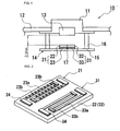
- [Fig. 1] Fig. 1 is a schematic diagram showing a structure of a multistage switch according to an embodiment of the present invention.
- [Fig. 2] Fig. 2 is a perspective view showing a structure of semiconductor magnetoresistive elements used in the multistage switch according to the embodiment of the present invention.
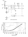
- [Fig. 3] Fig. 3 is a circuit diagram of the multistage switch according to the embodiment of the present invention.
- [Fig. 4] Fig. 4 is a graph showing the relationship between the distance from a magnetic member of a magnetic sensor used in the multistage switch according to the embodiment of the present invention and a detected potential.
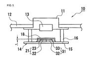
- [Fig. 5] Fig. 5 is a schematic diagram showing a structure of a multistage switch according to another embodiment of the present invention.
-
- 10
- multistage switch
- 11
- switch push button
- 13
- magnet
- 14
- magnetic sensor
- 15
- substrate
- 18
- package
- 21
- first magnetoelectric transducer
- 22
- base
- 23
- magnetosensitive section
- 23a
- semiconductor magnetoresistive thin film
- 23b
- short-circuiting electrode
- 24
- external electrode
- 31
- second magnetoelectric transducer
- 32
- base
- 33
- magnetosensitive section
- 33a
- semiconductor magnetoresistive thin film
- 33b
- short-circuiting electrode
- 34
- external electrode
- The features of the present invention will be described in more detail hereinafter with respect to embodiments of the present invention.
- A multistage switch according to an embodiment of the present invention will be described with reference to Figs. 1 and 2. The embodiment will be described in the context of a multistage switch used for a shutter of a camera by way of example.
- A
multistage switch 10 shown in Fig. 1 includes aswitch push button 11 serving as a shutter release button. Theswitch push button 11 is surrounded by ahousing 12 of the camera, and is generally projected slightly from the housing. Amagnet 13 serving as a magnetic member is disposed in a recess of the inner wall surface of theswitch push button 11. Themagnet 13 is disposed so that lines of magnetic force are generated in the direction in which theswitch push button 11 is pressed, i.e., in the direction indicated by an arrow shown in Fig. 1. In the present embodiment, the south pole of themagnet 13 is oriented toward the top of theswitch push button 11, and the north pole of themagnet 13 is oriented on the bottom side of the switch push button. - The
multistage switch 10 further includes amagnetic sensor 14. Themagnetic sensor 14 includes asubstrate 15 defining a main circuit of the sensor. Thesubstrate 15 is made of, for example, a glass epoxy material or ceramic material. Twomagnetoelectric transducers substrate 15. These twomagnetoelectric transducers magnet 13. - In the
multistage switch 10, weak reaction force is only required to return theswitch push button 11 to the initial position, and a weak spring, a low-repulsive material, or the like can be provided between theswitch push button 11 and thesubstrate 15. In the present embodiment, a low-repulsive material 16 is used. - In the present embodiment, the two
magnetoelectric transducers bases bases magnetosensitive sections magnetoelectric transducers magnetosensitive sections substrate 15. Themagnetoelectric transducers electroconductive adhesive 17. - The structure of the two
magnetoelectric transducers - Fig. 2 shows two semiconductor magnetoresistive elements used as the two
magnetoelectric transducers - The two
magnetoelectric transducers bases - On the
base 22 of the firstmagnetoelectric transducer 21 of the twomagnetoelectric transducers thin film 23a made of InSb (indium antimonide) is defined in a meandering line pattern. The semiconductor magnetoresistivethin film 23a is generally formed using vacuum deposition. A plurality of multi-layered short-circuiting electrodes 23b made of Ni/Cr/Au, Cr/Ni/Au, or the like are defined on the semiconductor magnetoresistivethin film 23a. The short-circuiting electrodes 23b are formed into a multi-layer structure using a method such as vapor deposition or sputtering. In Fig. 2, however, the multi-layer structure is not shown for simplification of illustration. The semiconductor magnetoresistivethin film 23a and the short-circuiting electrodes 23b function as themagnetosensitive section 23. The firstmagnetoelectric transducer 21 further includes anexternal electrode 24 to be connected to a circuit pattern on thesubstrate 15 or the secondmagnetoelectric transducer 31. Theexternal electrode 24 is formed of the same electrode material using the same method as the short-circuiting electrodes 23b. - On the
base 32 of the secondmagnetoelectric transducer 31, a semiconductor magnetoresistivethin film 33a made of InSb (indium antimonide) is defined in a meandering line pattern. The semiconductor magnetoresistivethin film 33a is formed in the same shape, of the same electrode material, and using the same method as the semiconductor magnetoresistivethin film 23a of the firstmagnetoelectric transducer 21. A plurality of multi-layered short-circuiting electrodes 33b are defined on the semiconductor magnetoresistivethin film 33a. The number of defined short-circuiting electrodes 33b is smaller than the number of short-circuiting electrodes 23b defined on the firstmagnetoelectric transducer 21. The semiconductor magnetoresistivethin film 33a and the short-circuiting electrodes 33b function as themagnetosensitive section 33. The secondmagnetoelectric transducer 31 further includes anexternal electrode 34 to be connected to the circuit pattern of thesubstrate 15 or the firstmagnetoelectric transducer 21. - The first and second
magnetoelectric transducers magnetoelectric transducer 21 has a predetermined magnetic resistance change characteristic while substantially no magnetic resistance change occurs in the secondmagnetoelectric transducer 31. However, the first and secondmagnetoelectric transducers - The circuit structure of the
magnetic sensor 14 in themultistage switch 10 will now be described with reference to Fig. 3. - In the
magnetic sensor 14, the twomagnetoelectric transducers multistage switch 10 has two operating stages to be switched, first and second threshold values V1 and V2 are set in themagnetic sensor 14. - A voltage V at a node between the two
magnetoelectric transducers magnetic sensor 14, with the first threshold value V1 using a comparator C1, and is also compared with the second threshold value V2 using a comparator C2. An operation instruction is transmitted from themagnetic sensor 14 to the camera according to those comparison results. - If the multistage switch has n operating stages to be switched, as indicated by a two-dot chain line shown in Fig. 4, a circuit structure in which the voltage V is compared with the n-th threshold Vn using a comparator Cn may be used.
- The operation of the
multistage switch 10 having the above-described structure is as follows. - First, a user presses the
switch push button 11 to perform photographing using the camera. The pressedswitch push button 11 gradually approaches themagnetic sensor 14. Therefore, themagnet 13 in the switch push button approaches the first and secondmagnetoelectric transducers magnetic sensor 14. Then, the resistance value of the firstmagnetoelectric transducer 21 changes. The resistance value of the secondmagnetoelectric transducer 31 does not substantially change. The change in resistance value due to the approaching of themagnet 13 causes a change in the voltage V at the node between the twomagnetoelectric transducers magnetic sensor 14 to the camera according to those comparison results. - Although substantially no magnetic resistance change occurs in the second
magnetoelectric transducer 31, the resistance change characteristic of the secondmagnetoelectric transducer 31 due to the temperature change is substantially identical to that of the firstmagnetoelectric transducer 21. Therefore, the potential V at the node between the twomagnetoelectric transducers magnetoelectric transducer 21, i.e., the magnetic sensitivity. Since the temperature characteristics of the twomagnetoelectric transducers magnetoelectric transducers magnetoelectric transducers magnetic sensor 14 of the present embodiment is therefore a potential indicating a shift that purely depends on the magnetic change, in which the influence of a change in ambient temperature is canceled, in the shift in the potential of the firstmagnetoelectric transducer 21. - A specific operation example in which the number of stages in which the operation of the camera is switched is two, the first stage corresponding to the focusing operation of the camera and the second stage corresponding to the shutter release operation, will be described with reference to Figs. 1 and 4.
- As shown in Fig. 1, the distance between the
magnet 13 and the twomagnetoelectric transducers switch push button 11 is not pressed. As shown in Fig. 4, the voltage V at the node between themagnetoelectric transducers switch push button 11 can be pressed up to 1.7 mm. As shown in Fig. 4, the relationship between the pressing amount of the switch push button and the voltage V at the node between themagnetoelectric transducers - This characteristic is obtained because semiconductor magnetoresistive elements are used as the
magnetoelectric transducers magnet 13 is large, and the amount of change in the voltage value to be output is also large. Therefore, the output signal can be directly compared with the threshed values for determining the operation of themultistage switch 10. Further, the voltage V to be output permits a conversion efficiency of about 10% of the input voltage Vin applied to the two magnetoelectric transducers connected in series, and higher efficiency than various magnetoelectric transducers such as Hall elements and magnetoresistive elements formed of ferromagnetic metal thin films is attained, which is suitable for use in compact electronic apparatuses. - In the
multistage switch 10, as can be seen from the output characteristic shown in Fig. 4, as threshold values in the two-stage operation switching, for example, the first threshold value V1 is set to 2.7 V ± 0.05 V and the second threshold value V2 is set to be not less than 2.9 V to ensure a difference of 0.4 mm in the pressing amount of theswitch push button 11 from the first threshold value V1 to the second threshold value V2. A voltage value serving as a threshold value may be set as a range, like the first threshold value V1, or may be set as a boundary, like the second threshold value V2, e.g., whether or not the voltage value exceeds 2.9 V. In the present embodiment, the first threshold value V1 is used for focusing and is given a certain range. If the voltage exceeds the range and is near the second threshold value V2, the focusing operation is canceled. Therefore, the user can understand that the pressing amount of theswitch push button 11 has advanced too much. Since the operation corresponding to the second threshold value V2 is the shutter release operation, the second threshold value V2 is not given a specific range and is set so that the operation is performed if the voltage V exceeds the second threshold value V2. Even if the first threshold value V1 is used for the focusing operation, the first threshold value V1 may not be given a range and may be set to, for example, 2.7 V so that the focusing operation can be performed if the voltage V exceeds the threshold value of 2.7 V. - In the
multistage switch 10 of the present invention, therefore, since the voltage V serving as a detected potential linearly changes, it is easy to set a threshed value for the multistage switch. Further, the number of stages can be increased only with a simple circuit design. Therefore, multiple stages more than two stages can easily be set, which is substantially impossible in a multistage sensor using disc springs as described in the related art. - In the present embodiment, a semiconductor magnetoresistive element is used as a magnetoelectric transducer. Instead of a semiconductor magnetoresistive element, a Hall element or a ferromagnetic magnetoresistive element can be used because similar advantages are achieved without generating strong reaction force when the switch push button is pressed. However, the conversion efficiency of a Hall element or a ferromagnetic magnetoresistive element with respect to an input voltage is lower than that of a semiconductor magnetoresistive element. Therefore, preferably, a semiconductor magnetoresistive element is used as a magnetoelectric transducer in a multistage switch of a compact electronic apparatus.
- Further, in the present embodiment, a switch push button and a magnet are separately provided by way of example. However, a switch push button formed by combining a magnetic member having magnetic properties with a switch push button into a single unit, e.g., a switch push button made of plastic magnet, may be used.
- Further, in the present embodiment, a semiconductor magnetoresistive element is used as a magnetoelectric transducer and is mounted on a substrate using flip-chip bonding by way of example. A magnetosensitive section may be mounted using wire bonding so as to face a magnetic member.
- Further, in the present embodiment, two magnetoelectric transducers are used, of which the second magnetoelectric transducer has a lower magnetic sensitivity and is used as a magnetoelectric transducer for temperature compensation. For example, the second magnetoelectric transducer may be mounted on a corner of a substrate and disposed at a position that is not affected by magnetic force. Thereby, the second magnetoelectric transducer can be the same as the first magnetoelectric transducer, and can also be used for temperature compensation. However, in this case, since the size of the substrate is large, the structure of the present invention in which the magnetic sensitivity of the second magnetoelectric transducer is reduced and the first and second magnetoelectric transducers are disposed adjacent to each other is suitable for use in compact electronic apparatuses.
- While in the present embodiment, the operation mechanism of the switch push button has been described in the context of a weak spring or a low-repulsive material, the operation mechanism is not limited thereto. Not only a physical operation mechanism but also an operation mechanism that is controlled by an electrical signal can be used as far as the operation mechanism of the switch push button is independent from an operation signal system of the magnetic sensor, that is, an operation mechanism that is not related to an operation signal of the magnetic sensor.
- In the present embodiment, the magnetic sensor is not provided with a package. For example, as shown in Fig. 5, the
magnetic sensor 14 may be configured such that themagnetoelectric transducers package 18. In Fig. 5, themagnetoelectric transducers magnetosensitive sections bases substrate 15. In Fig. 5, wires are not shown. In general, wires formed of gold or aluminum wires having a line diameter of 50 µm are used, and ball bonding or wedge bending is performed. In packaging, a resin with flexibility is coated about 0.1 mm thick on the surface of the magnetoelectric transducers so that no stress is applied to loop (slack) portions or bonding portions of the wires. Then, the magnetoelectric transducers are packaged with a high-fluidity resin. The thickness of the resin used for packaging is reduced as much as possible to increase the used range of the output characteristic. However, if the thickness is too thin, the physical strength of the elements is reduced. Therefore, preferably, the package thickness is about 0.15 to 0.20 mm. The package design is done so that a spacing t between thepackage 18 and themagnetosensitive sections magnetoelectric transducers switch push button 11. - As described above, a multistage switch of the present invention allows a user to smoothly press a switch push button without being subjected to strong physical reaction force such as force of disc springs. Therefore, particularly when the multistage switch is used in a camera or the like, the focusing operation corresponding to the operating state of the first stage can be performed with a low possibility of occurrence of camera-shake, etc.
- Further, even if the moving distance of the switch push button is small, an output characteristic having a large output value with respect to a small change in magnetic force caused by the change in the distance can be obtained. Furthermore, the output characteristic exhibits an improved linearity, and it is easy to set threshed values for multiple stages. Therefore, the multistage switch used in a camera can be used not only as a multistage switch used for two operations of focusing and releasing a shutter but also as a multistage switch to be operated in a larger number of stages. For example, a stage for preparing the camera for the shutter release operation can be provided between the focusing stage and the actual shutter release stage, or a stage for performing photographing substantially at the same time as the actual shutter release operation, etc., can be provided. Consequently, no time error is produced between the timing of releasing a shutter in a digital camera and the timing of actually photographing a subject.
Claims (6)
- A multistage switch comprising:a magnetic sensor includinga substrate, anda magnetoelectric transducer defined on the substrate;a switch push button; anda magnetic member provided in the switch push button and disposed so as to face the magnetoelectric transducer,wherein the magnetic sensor detects, as a detected potential, a potential produced at the magnetoelectric transducer in the magnetic sensor by a shift in a distance between the magnetic sensor and the magnetic member, andat least two threshold values are provided for the detected potential, and an operating state is changed according to results of comparison between the threshold values and the detected potential.
- The multistage switch according to Claim 1, wherein the magnetoelectric transducer comprises a semiconductor magnetoresistive element.
- The multistage switch according to Claim 1 or 2, wherein the magnetic sensor includes two magnetoelectric transducers connected in series,
the detected potential is a detected potential at a node between the two magnetoelectric transducers, and
a first magnetoelectric transducer of the two magnetoelectric transducers has a predetermined shift in a potential produced by a shift in a distance between the first magnetoelectric transducer and the magnetic member, and a second magnetoelectric transducer of the two magnetoelectric transducers has substantially no shift in a potential produced by a shift in a distance between the second magnetoelectric transducer and the magnetic member, and the first magnetoelectric transducer and the second magnetoelectric transducer have substantially identical temperature characteristics. - The multistage switch according to Claim 3, wherein the first magnetoelectric transducer comprises a semiconductor magnetoresistive element, including a semiconductor magnetoresistive thin film defined on a base, a plurality of short-circuiting electrodes defined on the semiconductor magnetoresistive thin film, and an external electrode connected to the outside, and
the second magnetoelectric transducer comprises a semiconductor magnetoresistive element, including a semiconductor magnetoresistive thin film defined on the base, and an external electrode connected to the outside, and including, on the semiconductor magnetoresistive thin film, no short-circuiting electrodes or a smaller number of short-circuiting electrodes than the number of short-circuiting electrodes included in the first magnetoelectric transducer. - The multistage switch according to any of Claims 1 to 4, wherein a moving mechanism of the switch push button is independent from an operation signal system in the magnetic sensor.
- The multistage switch according to any of Claims 1 to 5, wherein the magnetic sensor includes a package covering the magnetoelectric transducer, and the package is disposed on the magnetic sensor so that a spacing between the package and a magnetosensitive section of the magnetoelectric transducer is set to be not more than 0.3 mm.
Applications Claiming Priority (2)
| Application Number | Priority Date | Filing Date | Title |
|---|---|---|---|
| JP2005011996 | 2005-01-19 | ||
| PCT/JP2006/300483 WO2006077807A1 (en) | 2005-01-19 | 2006-01-17 | Multistage switch |
Publications (3)
| Publication Number | Publication Date |
|---|---|
| EP1845542A1 true EP1845542A1 (en) | 2007-10-17 |
| EP1845542A4 EP1845542A4 (en) | 2008-02-27 |
| EP1845542B1 EP1845542B1 (en) | 2009-10-07 |
Family
ID=36692196
Family Applications (1)
| Application Number | Title | Priority Date | Filing Date |
|---|---|---|---|
| EP06711763A Expired - Lifetime EP1845542B1 (en) | 2005-01-19 | 2006-01-17 | Multistage switch |
Country Status (5)
| Country | Link |
|---|---|
| US (1) | US7538282B2 (en) |
| EP (1) | EP1845542B1 (en) |
| JP (1) | JP4617319B2 (en) |
| DE (1) | DE602006009624D1 (en) |
| WO (1) | WO2006077807A1 (en) |
Families Citing this family (10)
| Publication number | Priority date | Publication date | Assignee | Title |
|---|---|---|---|---|
| JP4917522B2 (en) * | 2007-12-07 | 2012-04-18 | 株式会社東海理化電機製作所 | Position sensor |
| US9646008B2 (en) * | 2008-11-20 | 2017-05-09 | Sony Interactive Entertainment Inc. | Modifying virtual item states in conjunction with digital broadcast |
| JP2013134076A (en) * | 2011-12-26 | 2013-07-08 | Denso Corp | Current detection apparatus |
| JP6044378B2 (en) * | 2013-02-13 | 2016-12-14 | オムロン株式会社 | Switching device |
| US10275055B2 (en) | 2016-03-31 | 2019-04-30 | Azoteq (Pty) Ltd | Rotational sensing |
| CN113138580B (en) * | 2020-01-20 | 2023-08-25 | 青岛海尔洗衣机有限公司 | A household appliance control device, control system and control method thereof |
| ES3033775T3 (en) * | 2021-08-04 | 2025-08-07 | Schneider Electric Ind Sas | Electrical contactless switch |
| DE102023117239A1 (en) | 2023-06-29 | 2025-01-02 | Leica Camera Aktiengesellschaft | SHUTTER FOR A CAMERA AND CAMERA |
| DE102023117235A1 (en) | 2023-06-29 | 2025-01-02 | Leica Camera Aktiengesellschaft | SHUTTER FOR A CAMERA AND CAMERA |
| JP7634057B1 (en) * | 2023-09-26 | 2025-02-20 | 株式会社ヴァレオジャパン | Switching device |
Family Cites Families (14)
| Publication number | Priority date | Publication date | Assignee | Title |
|---|---|---|---|---|
| JPS4934675U (en) * | 1972-06-30 | 1974-03-27 | ||
| JPS522396B2 (en) | 1972-08-05 | 1977-01-21 | ||
| DE2534414A1 (en) * | 1975-08-01 | 1977-02-10 | Precision Electronic Component | Thin film semiconductive magnetoresistor - of indium antimonide or arsenide formed from deposited elemental layers |
| JPS5475284A (en) * | 1977-11-29 | 1979-06-15 | Asahi Chemical Ind | Threeeterminal magnetic reluctance effect element |
| JPS60237722A (en) * | 1984-05-11 | 1985-11-26 | Mitsubishi Electric Corp | Multistage push switch |
| JP2980215B2 (en) | 1992-03-04 | 1999-11-22 | シーケーディ 株式会社 | Magnetic sensor |
| DE19632525C1 (en) * | 1996-08-13 | 1997-07-03 | Leica Camera Gmbh | Multistage spring-loaded pushbutton switch e.g. for electronic photographic camera light metering |
| JP2000011827A (en) | 1998-06-23 | 2000-01-14 | Yazaki Corp | Magnetic element switch |
| JP2000057888A (en) * | 1998-08-11 | 2000-02-25 | Tokai Rika Co Ltd | Multistage switch |
| JP2000259321A (en) | 1999-03-11 | 2000-09-22 | Land Computer:Kk | Keyboard switch with air damper |
| GB2367346B (en) | 2000-09-28 | 2004-07-14 | Nokia Mobile Phones Ltd | Control device |
| JP4121941B2 (en) | 2001-01-19 | 2008-07-23 | 富士通コンポーネント株式会社 | Pointing device and portable information device |
| JP4121730B2 (en) * | 2001-01-19 | 2008-07-23 | 富士通コンポーネント株式会社 | Pointing device and portable information device |
| JP4500472B2 (en) | 2001-08-13 | 2010-07-14 | アルプス電気株式会社 | Magnetic switch and magnetic sensor |
-
2006
- 2006-01-17 EP EP06711763A patent/EP1845542B1/en not_active Expired - Lifetime
- 2006-01-17 JP JP2006553884A patent/JP4617319B2/en not_active Expired - Fee Related
- 2006-01-17 WO PCT/JP2006/300483 patent/WO2006077807A1/en not_active Ceased
- 2006-01-17 DE DE602006009624T patent/DE602006009624D1/en not_active Expired - Lifetime
-
2007
- 2007-07-19 US US11/780,089 patent/US7538282B2/en not_active Expired - Fee Related
Also Published As
| Publication number | Publication date |
|---|---|
| EP1845542A4 (en) | 2008-02-27 |
| EP1845542B1 (en) | 2009-10-07 |
| WO2006077807A1 (en) | 2006-07-27 |
| JPWO2006077807A1 (en) | 2008-06-19 |
| JP4617319B2 (en) | 2011-01-26 |
| US7538282B2 (en) | 2009-05-26 |
| US20070257753A1 (en) | 2007-11-08 |
| DE602006009624D1 (en) | 2009-11-19 |
Similar Documents
| Publication | Publication Date | Title |
|---|---|---|
| US7538282B2 (en) | Multistage switch | |
| US20240361561A1 (en) | Optical system | |
| CN101331385B (en) | Position detection device | |
| KR100847652B1 (en) | Pointing device | |
| JP4108401B2 (en) | Input device and mobile terminal | |
| JP4575153B2 (en) | Current measuring method and current measuring apparatus | |
| USRE46385E1 (en) | Driving control device and operation device | |
| KR20120049630A (en) | Multi-direction input device | |
| US12106893B2 (en) | Coil module, actuator provided with coil module, and method for manufacturing coil module | |
| US8000597B2 (en) | Input device | |
| US9013622B2 (en) | Operation device | |
| US20220163571A1 (en) | Current sensor | |
| JP2004354254A (en) | Current sensor | |
| JP2009036579A (en) | Magnetometric sensor package | |
| JP7763154B2 (en) | Semiconductor package and drive device | |
| KR20030003689A (en) | Small-sized image pickup module | |
| JP2004325207A (en) | End-measuring apparatus | |
| US20250280199A1 (en) | Piezo-actuated platforms for image sensor stabilization | |
| WO2020045419A1 (en) | Slide sensor | |
| EP3273213B1 (en) | Low cost overmolded leadframe force sensor with multiple mounting positions | |
| CN215449772U (en) | Optical system | |
| JP4881041B2 (en) | Magnetic sensor device | |
| US7550896B1 (en) | Piezoelectric actuator system with position detection function and method thereof | |
| KR100908033B1 (en) | Pointing device and electronic device having the same | |
| KR20120037151A (en) | Multi-direction input device |
Legal Events
| Date | Code | Title | Description |
|---|---|---|---|
| PUAI | Public reference made under article 153(3) epc to a published international application that has entered the european phase |
Free format text: ORIGINAL CODE: 0009012 |
|
| 17P | Request for examination filed |
Effective date: 20070817 |
|
| AK | Designated contracting states |
Kind code of ref document: A1 Designated state(s): AT BE BG CH CY CZ DE DK EE ES FI FR GB GR HU IE IS IT LI LT LU LV MC NL PL PT RO SE SI SK TR |
|
| A4 | Supplementary search report drawn up and despatched |
Effective date: 20080125 |
|
| DAX | Request for extension of the european patent (deleted) | ||
| 17Q | First examination report despatched |
Effective date: 20080723 |
|
| GRAP | Despatch of communication of intention to grant a patent |
Free format text: ORIGINAL CODE: EPIDOSNIGR1 |
|
| GRAS | Grant fee paid |
Free format text: ORIGINAL CODE: EPIDOSNIGR3 |
|
| GRAA | (expected) grant |
Free format text: ORIGINAL CODE: 0009210 |
|
| AK | Designated contracting states |
Kind code of ref document: B1 Designated state(s): AT BE BG CH CY CZ DE DK EE ES FI FR GB GR HU IE IS IT LI LT LU LV MC NL PL PT RO SE SI SK TR |
|
| REG | Reference to a national code |
Ref country code: GB Ref legal event code: FG4D |
|
| REG | Reference to a national code |
Ref country code: CH Ref legal event code: EP |
|
| REG | Reference to a national code |
Ref country code: IE Ref legal event code: FG4D |
|
| REF | Corresponds to: |
Ref document number: 602006009624 Country of ref document: DE Date of ref document: 20091119 Kind code of ref document: P |
|
| PG25 | Lapsed in a contracting state [announced via postgrant information from national office to epo] |
Ref country code: SI Free format text: LAPSE BECAUSE OF FAILURE TO SUBMIT A TRANSLATION OF THE DESCRIPTION OR TO PAY THE FEE WITHIN THE PRESCRIBED TIME-LIMIT Effective date: 20091007 |
|
| NLV1 | Nl: lapsed or annulled due to failure to fulfill the requirements of art. 29p and 29m of the patents act | ||
| LTIE | Lt: invalidation of european patent or patent extension |
Effective date: 20091007 |
|
| PG25 | Lapsed in a contracting state [announced via postgrant information from national office to epo] |
Ref country code: SE Free format text: LAPSE BECAUSE OF FAILURE TO SUBMIT A TRANSLATION OF THE DESCRIPTION OR TO PAY THE FEE WITHIN THE PRESCRIBED TIME-LIMIT Effective date: 20091007 Ref country code: PT Free format text: LAPSE BECAUSE OF FAILURE TO SUBMIT A TRANSLATION OF THE DESCRIPTION OR TO PAY THE FEE WITHIN THE PRESCRIBED TIME-LIMIT Effective date: 20100208 Ref country code: LT Free format text: LAPSE BECAUSE OF FAILURE TO SUBMIT A TRANSLATION OF THE DESCRIPTION OR TO PAY THE FEE WITHIN THE PRESCRIBED TIME-LIMIT Effective date: 20091007 Ref country code: IS Free format text: LAPSE BECAUSE OF FAILURE TO SUBMIT A TRANSLATION OF THE DESCRIPTION OR TO PAY THE FEE WITHIN THE PRESCRIBED TIME-LIMIT Effective date: 20100207 Ref country code: FI Free format text: LAPSE BECAUSE OF FAILURE TO SUBMIT A TRANSLATION OF THE DESCRIPTION OR TO PAY THE FEE WITHIN THE PRESCRIBED TIME-LIMIT Effective date: 20091007 Ref country code: ES Free format text: LAPSE BECAUSE OF FAILURE TO SUBMIT A TRANSLATION OF THE DESCRIPTION OR TO PAY THE FEE WITHIN THE PRESCRIBED TIME-LIMIT Effective date: 20100118 |
|
| PG25 | Lapsed in a contracting state [announced via postgrant information from national office to epo] |
Ref country code: PL Free format text: LAPSE BECAUSE OF FAILURE TO SUBMIT A TRANSLATION OF THE DESCRIPTION OR TO PAY THE FEE WITHIN THE PRESCRIBED TIME-LIMIT Effective date: 20091007 Ref country code: LV Free format text: LAPSE BECAUSE OF FAILURE TO SUBMIT A TRANSLATION OF THE DESCRIPTION OR TO PAY THE FEE WITHIN THE PRESCRIBED TIME-LIMIT Effective date: 20091007 |
|
| PG25 | Lapsed in a contracting state [announced via postgrant information from national office to epo] |
Ref country code: BE Free format text: LAPSE BECAUSE OF FAILURE TO SUBMIT A TRANSLATION OF THE DESCRIPTION OR TO PAY THE FEE WITHIN THE PRESCRIBED TIME-LIMIT Effective date: 20091007 Ref country code: AT Free format text: LAPSE BECAUSE OF FAILURE TO SUBMIT A TRANSLATION OF THE DESCRIPTION OR TO PAY THE FEE WITHIN THE PRESCRIBED TIME-LIMIT Effective date: 20091007 |
|
| PG25 | Lapsed in a contracting state [announced via postgrant information from national office to epo] |
Ref country code: RO Free format text: LAPSE BECAUSE OF FAILURE TO SUBMIT A TRANSLATION OF THE DESCRIPTION OR TO PAY THE FEE WITHIN THE PRESCRIBED TIME-LIMIT Effective date: 20091007 Ref country code: NL Free format text: LAPSE BECAUSE OF FAILURE TO SUBMIT A TRANSLATION OF THE DESCRIPTION OR TO PAY THE FEE WITHIN THE PRESCRIBED TIME-LIMIT Effective date: 20091007 Ref country code: EE Free format text: LAPSE BECAUSE OF FAILURE TO SUBMIT A TRANSLATION OF THE DESCRIPTION OR TO PAY THE FEE WITHIN THE PRESCRIBED TIME-LIMIT Effective date: 20091007 Ref country code: DK Free format text: LAPSE BECAUSE OF FAILURE TO SUBMIT A TRANSLATION OF THE DESCRIPTION OR TO PAY THE FEE WITHIN THE PRESCRIBED TIME-LIMIT Effective date: 20091007 Ref country code: BG Free format text: LAPSE BECAUSE OF FAILURE TO SUBMIT A TRANSLATION OF THE DESCRIPTION OR TO PAY THE FEE WITHIN THE PRESCRIBED TIME-LIMIT Effective date: 20100107 |
|
| PLBE | No opposition filed within time limit |
Free format text: ORIGINAL CODE: 0009261 |
|
| STAA | Information on the status of an ep patent application or granted ep patent |
Free format text: STATUS: NO OPPOSITION FILED WITHIN TIME LIMIT |
|
| PG25 | Lapsed in a contracting state [announced via postgrant information from national office to epo] |
Ref country code: SK Free format text: LAPSE BECAUSE OF FAILURE TO SUBMIT A TRANSLATION OF THE DESCRIPTION OR TO PAY THE FEE WITHIN THE PRESCRIBED TIME-LIMIT Effective date: 20091007 Ref country code: MC Free format text: LAPSE BECAUSE OF NON-PAYMENT OF DUE FEES Effective date: 20100131 Ref country code: CZ Free format text: LAPSE BECAUSE OF FAILURE TO SUBMIT A TRANSLATION OF THE DESCRIPTION OR TO PAY THE FEE WITHIN THE PRESCRIBED TIME-LIMIT Effective date: 20091007 |
|
| REG | Reference to a national code |
Ref country code: CH Ref legal event code: PL |
|
| 26N | No opposition filed |
Effective date: 20100708 |
|
| GBPC | Gb: european patent ceased through non-payment of renewal fee |
Effective date: 20100117 |
|
| REG | Reference to a national code |
Ref country code: FR Ref legal event code: ST Effective date: 20100930 |
|
| PG25 | Lapsed in a contracting state [announced via postgrant information from national office to epo] |
Ref country code: LI Free format text: LAPSE BECAUSE OF NON-PAYMENT OF DUE FEES Effective date: 20100131 Ref country code: GR Free format text: LAPSE BECAUSE OF FAILURE TO SUBMIT A TRANSLATION OF THE DESCRIPTION OR TO PAY THE FEE WITHIN THE PRESCRIBED TIME-LIMIT Effective date: 20100108 Ref country code: FR Free format text: LAPSE BECAUSE OF NON-PAYMENT OF DUE FEES Effective date: 20100201 Ref country code: CH Free format text: LAPSE BECAUSE OF NON-PAYMENT OF DUE FEES Effective date: 20100131 |
|
| PG25 | Lapsed in a contracting state [announced via postgrant information from national office to epo] |
Ref country code: GB Free format text: LAPSE BECAUSE OF NON-PAYMENT OF DUE FEES Effective date: 20100117 |
|
| PG25 | Lapsed in a contracting state [announced via postgrant information from national office to epo] |
Ref country code: IE Free format text: LAPSE BECAUSE OF NON-PAYMENT OF DUE FEES Effective date: 20100117 |
|
| PG25 | Lapsed in a contracting state [announced via postgrant information from national office to epo] |
Ref country code: IT Free format text: LAPSE BECAUSE OF FAILURE TO SUBMIT A TRANSLATION OF THE DESCRIPTION OR TO PAY THE FEE WITHIN THE PRESCRIBED TIME-LIMIT Effective date: 20091007 |
|
| PG25 | Lapsed in a contracting state [announced via postgrant information from national office to epo] |
Ref country code: CY Free format text: LAPSE BECAUSE OF FAILURE TO SUBMIT A TRANSLATION OF THE DESCRIPTION OR TO PAY THE FEE WITHIN THE PRESCRIBED TIME-LIMIT Effective date: 20091007 |
|
| PG25 | Lapsed in a contracting state [announced via postgrant information from national office to epo] |
Ref country code: LU Free format text: LAPSE BECAUSE OF NON-PAYMENT OF DUE FEES Effective date: 20100117 Ref country code: HU Free format text: LAPSE BECAUSE OF FAILURE TO SUBMIT A TRANSLATION OF THE DESCRIPTION OR TO PAY THE FEE WITHIN THE PRESCRIBED TIME-LIMIT Effective date: 20100408 |
|
| PG25 | Lapsed in a contracting state [announced via postgrant information from national office to epo] |
Ref country code: TR Free format text: LAPSE BECAUSE OF FAILURE TO SUBMIT A TRANSLATION OF THE DESCRIPTION OR TO PAY THE FEE WITHIN THE PRESCRIBED TIME-LIMIT Effective date: 20091007 |
|
| PGFP | Annual fee paid to national office [announced via postgrant information from national office to epo] |
Ref country code: DE Payment date: 20200121 Year of fee payment: 15 |
|
| REG | Reference to a national code |
Ref country code: DE Ref legal event code: R119 Ref document number: 602006009624 Country of ref document: DE |
|
| PG25 | Lapsed in a contracting state [announced via postgrant information from national office to epo] |
Ref country code: DE Free format text: LAPSE BECAUSE OF NON-PAYMENT OF DUE FEES Effective date: 20210803 |