EP1843464A1 - Voltage-to-current converter - Google Patents
Voltage-to-current converter Download PDFInfo
- Publication number
- EP1843464A1 EP1843464A1 EP06392006A EP06392006A EP1843464A1 EP 1843464 A1 EP1843464 A1 EP 1843464A1 EP 06392006 A EP06392006 A EP 06392006A EP 06392006 A EP06392006 A EP 06392006A EP 1843464 A1 EP1843464 A1 EP 1843464A1
- Authority
- EP
- European Patent Office
- Prior art keywords
- current
- voltage
- input
- pmos transistor
- circuit
- Prior art date
- Legal status (The legal status is an assumption and is not a legal conclusion. Google has not performed a legal analysis and makes no representation as to the accuracy of the status listed.)
- Granted
Links
- 230000010354 integration Effects 0.000 claims abstract description 24
- 238000000034 method Methods 0.000 claims abstract description 19
- 239000003990 capacitor Substances 0.000 claims description 9
- 230000001105 regulatory effect Effects 0.000 claims description 4
- 230000033228 biological regulation Effects 0.000 claims description 2
- 238000005516 engineering process Methods 0.000 description 4
- 238000010586 diagram Methods 0.000 description 3
- 238000006243 chemical reaction Methods 0.000 description 1
- 230000001419 dependent effect Effects 0.000 description 1
- 239000000463 material Substances 0.000 description 1
- 238000005259 measurement Methods 0.000 description 1
- 238000005070 sampling Methods 0.000 description 1
- 239000004065 semiconductor Substances 0.000 description 1
Images

Classifications
-
- H—ELECTRICITY
- H03—ELECTRONIC CIRCUITRY
- H03F—AMPLIFIERS
- H03F3/00—Amplifiers with only discharge tubes or only semiconductor devices as amplifying elements
- H03F3/45—Differential amplifiers
- H03F3/45071—Differential amplifiers with semiconductor devices only
- H03F3/45076—Differential amplifiers with semiconductor devices only characterised by the way of implementation of the active amplifying circuit in the differential amplifier
- H03F3/45179—Differential amplifiers with semiconductor devices only characterised by the way of implementation of the active amplifying circuit in the differential amplifier using MOSFET transistors as the active amplifying circuit
- H03F3/45183—Long tailed pairs
-
- H—ELECTRICITY
- H03—ELECTRONIC CIRCUITRY
- H03F—AMPLIFIERS
- H03F1/00—Details of amplifiers with only discharge tubes, only semiconductor devices or only unspecified devices as amplifying elements
- H03F1/32—Modifications of amplifiers to reduce non-linear distortion
-
- H—ELECTRICITY
- H03—ELECTRONIC CIRCUITRY
- H03F—AMPLIFIERS
- H03F3/00—Amplifiers with only discharge tubes or only semiconductor devices as amplifying elements
- H03F3/45—Differential amplifiers
- H03F3/45071—Differential amplifiers with semiconductor devices only
- H03F3/45479—Differential amplifiers with semiconductor devices only characterised by the way of common mode signal rejection
- H03F3/45632—Differential amplifiers with semiconductor devices only characterised by the way of common mode signal rejection in differential amplifiers with FET transistors as the active amplifying circuit
- H03F3/45636—Differential amplifiers with semiconductor devices only characterised by the way of common mode signal rejection in differential amplifiers with FET transistors as the active amplifying circuit by using feedback means
-
- H—ELECTRICITY
- H03—ELECTRONIC CIRCUITRY
- H03F—AMPLIFIERS
- H03F2200/00—Indexing scheme relating to amplifiers
- H03F2200/331—Sigma delta modulation being used in an amplifying circuit
Definitions
- This invention relates generally to voltage-to-current converters and relates more particularly to voltage-to-current converters circuits having very low noise and low Gm transconductance for applications as e.g. integrator circuits required in sigma-delta modulators.
- Voltage-to-current converters are required if an input voltage from e.g. any measurement device has to be converted to a current to drive a device depending on the current injected into or sunk through its input.
- a device depending upon a current injected could be an integrating capacitor of a Gm integrator.
- Gm integrators are often employed in measuring technology e.g. in connection with sigma-delta modulators. In this context it is very important to achieve very low noise and low Gm transconductance together with a high linearity. For these linearity requirements it is necessary to use integration resistors with a Gm integrator.
- U. S. Patent ( 7,002,501 to Gulati et al. ) proposes a reconfigurable ADC including a plurality of reconfigurable blocks for allowing the ADC to provide a plurality of architectures.
- the ADC can be configured to operate in a pipeline mode and a sigma-delta mode. This arrangement provides an ADC having a relatively large range of bandwidth and resolution.
- U. S. Patent discloses an over-sampling analog-to-digital converter using a current switching circuit as a local digital-to-analog converter, wherein a difference between the output currents of a voltage-to-current converter circuit and a current switching circuit is integrated by a capacitor of which the one end is grounded to a dc potential. Further, the current switching circuit has many bits to decrease the difference current between the signal current and the feedback current signal.
- the level-shifting function of the voltage-to-current converter circuit makes it possible to apparently subtract the dc component from the input analog signal, which is produced based on an internally generated dc voltage as a dc bias voltage, and to decrease a change in the voltage between the electrodes of a capacitor caused by the integration of current.
- U. S. Patent Application Publication ( 2005/0275575 to Motz ) discloses an integrator circuit having an integrator unit performed to generate an integrated signal from a modulated input signal. Additionally, the integrator circuit has an error feedback coupler connected to an output of the integrator unit and to an input of the integrator unit and formed to determine an error component from the integrated signal or from a signal derived from the integrated signal and to compensate the error component via the feedback in the modulated input signal.
- a principal object of the present invention is to achieve methods and circuits for a low noise and high linear voltage-to current converter.
- a further object of the present invention is to achieve voltage-to-current converter requiring only small integration resistors.
- a method to achieve a voltage-to-current converter having a high linearity and low noise comprises, first, the provision of an operational transconductance amplifier (OTA), resistive means for integration, DC current sources, and current mirrors.
- the next step of the method is shifting the level of the input voltages so far above ground voltage that input transistors of the OTA are kept in saturation mode.
- the last step is feeding back the output current to input current using current mirrors wherein the feedback current is larger than the output current.
- OTA operational transconductance amplifier
- a circuit for a voltage-to current converter having low noise and low transconductance has been achieved.
- the circuit invented comprises, first, a positive and a negative input voltage, and circuitry to shift said input voltages higher to enable an input stage of a differential operational transconductance amplifier (OTA) to operate in saturation mode for MOS devices.
- the core of the present invention is said differential OTA.
- This OTA comprises a circuitry for common mode decoupling of input from output wherein active loads are regulated in a way to achieve a correct output common mode voltage, and a positive and a negative output connected to a load, wherein these outputs have a transconductance in the order of magnitude of 1 Gm.
- the OTA comprises a positive and a negative output fed back to said correspondent input stages of the OTA, wherein these positive and negative outputs have a significant higher transconductance than said outputs being connected to said load and wherein said outputs fed back and outputs to said load are decoupled by means of current mirrors.
- a circuit for a voltage-to current converter having low noise and low transconductance comprises, first, a positive and a negative input voltage, a first circuitry connected between said positive input voltage and a gate of a first NMOS input transistor of a differential operational transconductance amplifier (OTA) to shift said input voltage higher to enable said first NMOS input transistor and a first current source to operate in saturation mode for MOS devices, a second circuitry connected between said negative input voltage and a gate of a second NMOS input transistor to shift said input voltage higher to enable said second NMOS input transistor and a first current source to operate in saturation mode for MOS devices.
- OTA operational transconductance amplifier
- Said OTA is the core of the present invention comprising said first NMOS input transistor, wherein its drain is connected to the drain and the gate of a first PMOS transistor, to the gate of a second PMOS transistor, and to the gate of a third PMOS transistor, and its gate is connected to the drain of a sixth PMOS transistor and to the drain of a seventh PMOS transistor, and said second NMOS input transistor, wherein its drain is connected to the drain and the gate of a fourth PMOS transistor, to the gate of a fifth PMOS transistor, and to the gate of the sixth PMOS transistor, and wherein its gate is connected to the drain of the third PMOS transistor and to the drain of a eighth PMOS transistor.
- Said first current source is connected between ground and the sources of said first and second NMOS transistors.
- the sources of the first to eighth PMOS transistors are connected to VDD voltage.
- the drain of the second PMOS transistor is connected to a positive terminal of a load and to a first terminal of a second current source, and the drain of a fifth PMOS transistor is connected to a negative terminal of a load and to a first terminal of a third current source.
- the gate of a seventh PMOS transistor is connected to a bias voltage and to a gate of the eighth PMOS transistor.
- the OTA comprises said second and third current source, wherein their second terminals are connected to ground.
- the preferred embodiments disclose methods and circuits for voltage-to-current converters used e.g. as Gm integrators having a high linearity without requiring large integration resistors, which produce white noise.
- Gm integrators are used with a delta-sigma modulator for battery management as disclosed in European patent application (docket number DS05-020), serial number 06392004.5 assigned to the Assignee of the present invention, filed-on March 20, 2006 and which is herein incorporated by simple reference.
- the present invention was developed by paying special attention to the possible use of a Gm integrator of a sigma-delta modulator, reference to this use is not to be construed as limiting the scope of this invention.
- the principle of the methods and circuits invented can be used also for many other voltage-to-current conversion applications requiring high linearity.
- CMOS-technology complementary metal-oxide-semiconductor
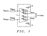
- Fig. 1 shows a schematic illustration of a preferred embodiment of the present invention.
- V IPOS At the positive input of the voltage-to-current converter used as differential Gm integrator 1 is voltage V IPOS
- V INEG At the negative input is voltage V INEG .
- integration resistors R IPOS and R INEG are used for linearization. The linearization can be performed either by means of resistors either in the source path of the input transistor pair, or by using resistors in the input branch shown in Fig. 1.
- MOS transistors operated in the linear region (acting like a resistor, not as a current source), could be used instead of these integration resistors R IPOS and R INEG .
- the G m integrator 1 is realized by an operational transconductance amplifier (OTA), which has a first nominal output of 1 Gm and a second output of 4 ⁇ G m .
- the output with the nominal G m is connected to a load 4 .
- the voltage-to-current converter is a Gm integrator this load would be an integration capacitor.
- the voltage-to-current converter of the present invention can be used to provide a linear current for a multitude of different loads as any device depending on the current injected into or sunk through its input.
- the additional 4 ⁇ G m output is fed back, due to the high feedback current allowing a significant reduction of the size of the integration resistors R IPOS and R INEG .
- Additional DC current sources 2 and 3 with equal sign for positive and negative feedback path perform the DC level shift from the differential input tied between VSS and the differential input of the OTA. Other ratios of feedback current to integration current are also possible.
- Fig. 2 shows a more detailed circuit diagram of a preferred embodiment of a voltage-to-current converter used as Gm integrator having low noise and a high linearity.
- the input voltage is applied at V IPOS and V INEG .
- the input voltages are level shifted to V DPOS and V DNEG by using the resistors R IPOS and R INEG and a current flowing through these resistors.
- the currents through the resistors are composed of a DC component I DCPOS and I DCNEG , and a current that is proportional to the integration current that is derived from the current mirror of the input stage to the output stage.
- Transistors M 1P , M 1N , M 2P , M 2N belong to the input stage.
- the other transistors belong to the feedback path (M 3 p, M 3N ,) or the output stage or output path (M 5P , M 5N ,).
- the advantage of the level shift is that the voltages V DPOS and V DNEG are so far above ground voltage, that the input transistors M 1P , M 1N , and the current source I DIFF are kept in normal operation, that is saturation mode for MOS devices, even if enhancement MOS devices with threshold voltages (V TH ) above zero are used.
- the additional constant DC current source I DIFF overlays the signal dependent current.
- V BIAS is the gate node of the current mirror M 4P to M 4N .
- V BIAS is preferably connected to a PMOS transistor with same channel length as M 4P to M 4N , whereas this transistor has gate and drain shorted and a current is forced through this device to generate the voltage V BIAS .
- the core of the disclosed voltage-to-current converter used as Gm integrator is an OTA comprising the input transistors M 1P , M 1N , the output current mirrors M 2P to M 5P and M 2N to M 5N , and active loads I OPOS and I ONEG connected to the output nodes V OPOS and V ONEG .
- the active loads I OPOS and I ONEG are regulated in a way to achieve the correct output common mode voltage.
- CMR Common mode regulation
- the output currents I LP and I LN are integrated on the capacitors C POS and C NEG .
- a capacitor having one terminal connected with node V OPOS and one terminal connected to node V ONEG could be used as integration capacitor.
- a load could be connected between node V OPOS and node V ONEG .
- the output current between both nodes could be input current to any other current driven devices.
- the current mirrors M 2P to M 5P and M 2N to M 5N can have a ratio smaller than 1 to establish a very small transconductance if required.
- the circuit disclosed here uses a second set of current mirrors M 2P to M 3P and M 2N to M 3N , with a ratio larger or different to the output current mirrors, to feed a larger current back to the resistors R IPOS and R INEG that specify or impact the transconductance.
- the total transconductance is not only specified by the resistors, but also from the dimensioning of the other parts of the circuit). Due to the high currents through the resistors R IPOS and R INEG can kept small. The resistors linearize the transconductance of the input stage M 1P and M 1N .
- the key feature of the circuit is that the integration current and the feedback current can be adjusted independently from each other by adjusting the ratio of the related current mirrors. This makes very small transconductances possible, without excessive increase of thermal noise of the resistors that control the transconductance.
- Gm can be determined by the design parameters (W/L) of the input transistors of the OTA, or accordingly by using linearization resistors inside or outside the OTA.
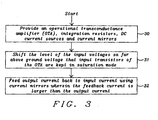
- Fig. 3 shows a flowchart of a method to achieve a voltage-to-current converter having a high linearity and low noise.
- Step 30 of the method invented illustrates the provision of an operational transconductance amplifier (OTA), integration resistors, DC current sources and current mirrors
- the following step 31 shows the shifting of the level of the input voltages so far above ground voltage that input transistors of the OTA are kept in saturation mode. The shifting of the input voltages can be performed by said integration resistors and a high current.
- the last step 32 describes the feedback of the output current to input current using current mirrors wherein the feedback current is larger than the output current. For example in the preferred embodiment shown in Fig. 1 the feedback current is 4xtimes larger than the output current.
Landscapes
- Engineering & Computer Science (AREA)
- Power Engineering (AREA)
- Physics & Mathematics (AREA)
- Nonlinear Science (AREA)
- Amplifiers (AREA)
Abstract
Description
- This invention relates generally to voltage-to-current converters and relates more particularly to voltage-to-current converters circuits having very low noise and low Gm transconductance for applications as e.g. integrator circuits required in sigma-delta modulators.
- Voltage-to-current converters are required if an input voltage from e.g. any measurement device has to be converted to a current to drive a device depending on the current injected into or sunk through its input. Such a device depending upon a current injected could be an integrating capacitor of a Gm integrator. Gm integrators are often employed in measuring technology e.g. in connection with sigma-delta modulators. In this context it is very important to achieve very low noise and low Gm transconductance together with a high linearity. For these linearity requirements it is necessary to use integration resistors with a Gm integrator.
- It is a challenge for the designers of voltage-to-current converters used e.g. as Gm integrators in sigma-delta modulators to achieve low noise and low offset continuous time Gm integrators combining small integration resistors and high linearity, together with small chip size and a very low clock frequency
- There are more known patents dealing with the design of integrator circuits.
- U. S. Patent (
7,002,501 to Gulati et al. ) proposes a reconfigurable ADC including a plurality of reconfigurable blocks for allowing the ADC to provide a plurality of architectures. In one embodiment, the ADC can be configured to operate in a pipeline mode and a sigma-delta mode. This arrangement provides an ADC having a relatively large range of bandwidth and resolution. - U. S. Patent (
5,227,795 to Yamakido et al. ) discloses an over-sampling analog-to-digital converter using a current switching circuit as a local digital-to-analog converter, wherein a difference between the output currents of a voltage-to-current converter circuit and a current switching circuit is integrated by a capacitor of which the one end is grounded to a dc potential. Further, the current switching circuit has many bits to decrease the difference current between the signal current and the feedback current signal. Moreover, the level-shifting function of the voltage-to-current converter circuit makes it possible to apparently subtract the dc component from the input analog signal, which is produced based on an internally generated dc voltage as a dc bias voltage, and to decrease a change in the voltage between the electrodes of a capacitor caused by the integration of current. - U. S. Patent Application Publication (
2005/0275575 to Motz ) discloses an integrator circuit having an integrator unit performed to generate an integrated signal from a modulated input signal. Additionally, the integrator circuit has an error feedback coupler connected to an output of the integrator unit and to an input of the integrator unit and formed to determine an error component from the integrated signal or from a signal derived from the integrated signal and to compensate the error component via the feedback in the modulated input signal. - A principal object of the present invention is to achieve methods and circuits for a low noise and high linear voltage-to current converter.
- A further object of the present invention is to achieve voltage-to-current converter requiring only small integration resistors.
- In accordance with the objects of this invention a method to achieve a voltage-to-current converter having a high linearity and low noise has been achieved. The method comprises, first, the provision of an operational transconductance amplifier (OTA), resistive means for integration, DC current sources, and current mirrors. The next step of the method is shifting the level of the input voltages so far above ground voltage that input transistors of the OTA are kept in saturation mode. The last step is feeding back the output current to input current using current mirrors wherein the feedback current is larger than the output current.
- In accordance with the objects of this invention a circuit for a voltage-to current converter having low noise and low transconductance has been achieved. The circuit invented comprises, first, a positive and a negative input voltage, and circuitry to shift said input voltages higher to enable an input stage of a differential operational transconductance amplifier (OTA) to operate in saturation mode for MOS devices. The core of the present invention is said differential OTA. This OTA comprises a circuitry for common mode decoupling of input from output wherein active loads are regulated in a way to achieve a correct output common mode voltage, and a positive and a negative output connected to a load, wherein these outputs have a transconductance in the order of magnitude of 1 Gm. Furthermore the OTA comprises a positive and a negative output fed back to said correspondent input stages of the OTA, wherein these positive and negative outputs have a significant higher transconductance than said outputs being connected to said load and wherein said outputs fed back and outputs to said load are decoupled by means of current mirrors.
- In accordance with further objects of this invention a circuit for a voltage-to current converter having low noise and low transconductance has been achieved. The circuit invented comprises, first, a positive and a negative input voltage, a first circuitry connected between said positive input voltage and a gate of a first NMOS input transistor of a differential operational transconductance amplifier (OTA) to shift said input voltage higher to enable said first NMOS input transistor and a first current source to operate in saturation mode for MOS devices, a second circuitry connected between said negative input voltage and a gate of a second NMOS input transistor to shift said input voltage higher to enable said second NMOS input transistor and a first current source to operate in saturation mode for MOS devices. Said OTA is the core of the present invention comprising said first NMOS input transistor, wherein its drain is connected to the drain and the gate of a first PMOS transistor, to the gate of a second PMOS transistor, and to the gate of a third PMOS transistor, and its gate is connected to the drain of a sixth PMOS transistor and to the drain of a seventh PMOS transistor, and said second NMOS input transistor, wherein its drain is connected to the drain and the gate of a fourth PMOS transistor, to the gate of a fifth PMOS transistor, and to the gate of the sixth PMOS transistor, and wherein its gate is connected to the drain of the third PMOS transistor and to the drain of a eighth PMOS transistor. Said first current source is connected between ground and the sources of said first and second NMOS transistors. The sources of the first to eighth PMOS transistors are connected to VDD voltage. The drain of the second PMOS transistor is connected to a positive terminal of a load and to a first terminal of a second current source, and the drain of a fifth PMOS transistor is connected to a negative terminal of a load and to a first terminal of a third current source. The gate of a seventh PMOS transistor is connected to a bias voltage and to a gate of the eighth PMOS transistor. Finally the OTA comprises said second and third current source, wherein their second terminals are connected to ground.
- In the accompanying drawings forming a material part of this description, there is shown:
- Fig. 1 shows a schematic block diagram of the voltage-to-current converter invented.
- Fig. 2 shows a detailed circuit diagram of a preferred embodiment of the voltage-to-current converter invented used as a Gm integrator.
- Fig. 3 shows a flowchart of a method to achieve a voltage-to-current converter having low noise and low transconductance.
- The preferred embodiments disclose methods and circuits for voltage-to-current converters used e.g. as Gm integrators having a high linearity without requiring large integration resistors, which produce white noise. In a preferred embodiment such Gm integrators are used with a delta-sigma modulator for battery management as disclosed in European patent application (docket number DS05-020), serial number 06392004.5 assigned to the Assignee of the present invention, filed-on March 20, 2006 and which is herein incorporated by simple reference. While the present invention was developed by paying special attention to the possible use of a Gm integrator of a sigma-delta modulator, reference to this use is not to be construed as limiting the scope of this invention. The principle of the methods and circuits invented can be used also for many other voltage-to-current conversion applications requiring high linearity.
- The preferred embodiments have been implemented in an integrated circuit (IC) using CMOS-technology; other semiconductor technologies are also possible.
- Fig. 1 shows a schematic illustration of a preferred embodiment of the present invention. At the positive input of the voltage-to-current converter used as
differential Gm integrator 1 is voltage VIPOS, at the negative input is voltage VINEG . For linearization of theGm integrator 1 integration resistors RIPOS and RINEG are used. The linearization can be performed either by means of resistors either in the source path of the input transistor pair, or by using resistors in the input branch shown in Fig. 1. Alternatively MOS transistors operated in the linear region (acting like a resistor, not as a current source), could be used instead of these integration resistors RIPOS and RINEG . - The Gm integrator 1 is realized by an operational transconductance amplifier (OTA), which has a first nominal output of 1 Gm and a second output of 4·Gm. The output with the nominal Gm is connected to a
load 4. In case the voltage-to-current converter is a Gm integrator this load would be an integration capacitor. The voltage-to-current converter of the present invention can be used to provide a linear current for a multitude of different loads as any device depending on the current injected into or sunk through its input. The additional 4·Gm output is fed back, due to the high feedback current allowing a significant reduction of the size of the integration resistors RIPOS and RINEG . Additional DCcurrent sources - Fig. 2 shows a more detailed circuit diagram of a preferred embodiment of a voltage-to-current converter used as Gm integrator having low noise and a high linearity. The input voltage is applied at VIPOS and VINEG . The input voltages are level shifted to VDPOS and VDNEG by using the resistors RIPOS and RINEG and a current flowing through these resistors. The currents through the resistors are composed of a DC component IDCPOS and IDCNEG , and a current that is proportional to the integration current that is derived from the current mirror of the input stage to the output stage. Transistors M1P, M1N, M2P, M2N belong to the input stage. The other transistors belong to the feedback path (M3p, M3N,) or the output stage or output path (M5P, M5N,).
- The advantage of the level shift is that the voltages VDPOS and VDNEG are so far above ground voltage, that the input transistors M1P, M1N, and the current source IDIFF are kept in normal operation, that is saturation mode for MOS devices, even if enhancement MOS devices with threshold voltages (VTH) above zero are used. The additional constant DC current source IDIFF overlays the signal dependent current.
- The voltage VBIAS is the gate node of the current mirror M4P to M4N. VBIAS is preferably connected to a PMOS transistor with same channel length as M4P to M4N , whereas this transistor has gate and drain shorted and a current is forced through this device to generate the voltage VBIAS .
- The core of the disclosed voltage-to-current converter used as Gm integrator is an OTA comprising the input transistors M1P, M1N, the output current mirrors M2P to M5P and M2N to M5N, and active loads IOPOS and IONEG connected to the output nodes VOPOS and VONEG. The active loads I OPOS and IONEG are regulated in a way to achieve the correct output common mode voltage.
- Usually a circuit called "Common mode regulation" (CMR) is used to adjust the active loads IOPOS and I ONEG. This CMR circuit calculates the average of both output voltages and compares this value with a given reference common mode voltage. The difference between actual common mode voltage and the given reference is used to regulate the active load. Usually both current sources IOPOS and IONEG are identical as they do not contribute to the differential component of the output voltage.
- The output currents ILP and ILN are integrated on the capacitors CPOS and CNEG. Alternatively a capacitor having one terminal connected with node VOPOS and one terminal connected to node VONEG could be used as integration capacitor.
- For any other application of the voltage-to-current converter of the present invention a load could be connected between node VOPOS and node VONEG . The output current between both nodes could be input current to any other current driven devices.
- The current mirrors M2P to M5P and M2N to M5N can have a ratio smaller than 1 to establish a very small transconductance if required.
- A problem with very small transconductances is that it will require very large resistors, which cost a lot of area in most CMOS technologies, and which increases the thermal noise level due to the well known formula Vn = 4•k•T•R. The circuit disclosed here uses a second set of current mirrors M2P to M3P and M2N to M3N, with a ratio larger or different to the output current mirrors, to feed a larger current back to the resistors RIPOS and RINEG that specify or impact the transconductance. (The total transconductance is not only specified by the resistors, but also from the dimensioning of the other parts of the circuit). Due to the high currents through the resistors RIPOS and RINEG can kept small. The resistors linearize the transconductance of the input stage M1P and M1N.
- The key feature of the circuit is that the integration current and the feedback current can be adjusted independently from each other by adjusting the ratio of the related current mirrors. This makes very small transconductances possible, without excessive increase of thermal noise of the resistors that control the transconductance.
- The exact value of Gm can be determined by the design parameters (W/L) of the input transistors of the OTA, or accordingly by using linearization resistors inside or outside the OTA.
- Fig. 3 shows a flowchart of a method to achieve a voltage-to-current converter having a high linearity and low noise.
Step 30 of the method invented illustrates the provision of an operational transconductance amplifier (OTA), integration resistors, DC current sources and current mirrors The followingstep 31 shows the shifting of the level of the input voltages so far above ground voltage that input transistors of the OTA are kept in saturation mode. The shifting of the input voltages can be performed by said integration resistors and a high current. Thelast step 32 describes the feedback of the output current to input current using current mirrors wherein the feedback current is larger than the output current. For example in the preferred embodiment shown in Fig. 1 the feedback current is 4xtimes larger than the output current. - While the invention has been particularly shown and described with reference to the preferred embodiments thereof, it will be understood by those skilled in the art that various changes in form and details may be made without departing from the spirit and scope of the invention.
Claims (21)
said fourth PMOS transistor, wherein its source is connected to VDD voltage;
said fifth PMOS transistor, wherein its source is connected to VDD voltage and its drain is connected to a negative terminal of a load and to a first terminal of a third current source;
said seventh PMOS transistor, wherein its source is connected to VDD voltage and its gate is connected to a bias voltage and to a gate of the eighth PMOS transistor;
said second current source, wherein its second terminal is connected to ground; and
Priority Applications (2)
| Application Number | Priority Date | Filing Date | Title |
|---|---|---|---|
| EP06392006A EP1843464B1 (en) | 2006-04-04 | 2006-04-04 | Voltage-to-current converter |
| US11/403,735 US7514999B2 (en) | 2006-04-04 | 2006-04-13 | Voltage-to-current converter |
Applications Claiming Priority (1)
| Application Number | Priority Date | Filing Date | Title |
|---|---|---|---|
| EP06392006A EP1843464B1 (en) | 2006-04-04 | 2006-04-04 | Voltage-to-current converter |
Publications (2)
| Publication Number | Publication Date |
|---|---|
| EP1843464A1 true EP1843464A1 (en) | 2007-10-10 |
| EP1843464B1 EP1843464B1 (en) | 2012-10-17 |
Family
ID=38008327
Family Applications (1)
| Application Number | Title | Priority Date | Filing Date |
|---|---|---|---|
| EP06392006A Expired - Lifetime EP1843464B1 (en) | 2006-04-04 | 2006-04-04 | Voltage-to-current converter |
Country Status (2)
| Country | Link |
|---|---|
| US (1) | US7514999B2 (en) |
| EP (1) | EP1843464B1 (en) |
Families Citing this family (11)
| Publication number | Priority date | Publication date | Assignee | Title |
|---|---|---|---|---|
| EP2200176A1 (en) | 2008-12-19 | 2010-06-23 | Dialog Semiconductor GmbH | Adjustable integrator using a single capacitance |
| US7830197B2 (en) * | 2008-12-22 | 2010-11-09 | Dialog Semiconductor Gmbh | Adjustable integrator using a single capacitance |
| WO2012002496A1 (en) * | 2010-07-01 | 2012-01-05 | パナソニック電工株式会社 | Target object detection device |
| US8436620B2 (en) | 2010-09-02 | 2013-05-07 | Texas Instruments Incorporated | Voltage monitoring using bitstream signal processing |
| CN102636732B (en) * | 2012-04-17 | 2014-04-16 | 山西太钢不锈钢股份有限公司 | Method for searching for 10kV power grid grounding based on six-sigma tool |
| US8841938B2 (en) | 2013-01-11 | 2014-09-23 | Hon Hai Precision Industry Co., Ltd. | Voltage to current converter |
| CN105262443B (en) * | 2015-11-12 | 2017-11-14 | 电子科技大学 | A kind of High Linear low-noise trans-conductance amplifier |
| US10845832B2 (en) | 2018-09-10 | 2020-11-24 | Analog Devices International Unlimited Company | Voltage-to-current converter |
| US10541675B1 (en) * | 2018-11-15 | 2020-01-21 | King Fahd University Of Petroleum And Minerals | Multi-gain transconductance amplifier |
| IT202000004159A1 (en) * | 2020-02-28 | 2021-08-28 | St Microelectronics Srl | Corresponding voltage-to-current converter, device and procedure |
| CN114564067B (en) * | 2022-02-18 | 2024-05-24 | 上海灿瑞科技股份有限公司 | A low dropout linear regulator with high power supply rejection ratio |
Citations (6)
| Publication number | Priority date | Publication date | Assignee | Title |
|---|---|---|---|---|
| EP0208365A1 (en) * | 1985-07-01 | 1987-01-14 | Koninklijke Philips Electronics N.V. | Voltage-current converter |
| US5043652A (en) * | 1990-10-01 | 1991-08-27 | Motorola, Inc. | Differential voltage to differential current conversion circuit having linear output |
| EP0620513A1 (en) * | 1993-04-16 | 1994-10-19 | Koninklijke Philips Electronics N.V. | Balanced voltage-to-current converter with quiescent current control |
| US6060870A (en) * | 1997-03-13 | 2000-05-09 | U.S. Philips Corporation | Voltage-to-current converter with error correction |
| JP2002026666A (en) * | 2000-07-06 | 2002-01-25 | Matsushita Electric Ind Co Ltd | Voltage-current converter |
| WO2003038994A1 (en) * | 2001-10-27 | 2003-05-08 | Koninklijke Philips Electronics N.V. | Balanced transconductor and electronic device |
Family Cites Families (8)
| Publication number | Priority date | Publication date | Assignee | Title |
|---|---|---|---|---|
| US4965529A (en) * | 1989-09-21 | 1990-10-23 | The United States Of America As Represented By The Secretary Of Commerce | High current, very wide band transconductance amplifier |
| JP3039809B2 (en) | 1990-05-31 | 2000-05-08 | 株式会社日立製作所 | Analog / digital converter, sampling pulse generation circuit, and current switch circuit |
| JPH09238032A (en) * | 1996-02-29 | 1997-09-09 | Nec Corp | Ota and bipolar multiplier |
| WO2000065723A1 (en) | 1999-04-21 | 2000-11-02 | Koninklijke Philips Electronics N.V. | Sigma-delta analog-to-digital converter |
| CA2298310C (en) * | 2000-02-09 | 2003-07-29 | James A. Cherry | Low-voltage transconductance amplifier/filters |
| US6686860B2 (en) | 2000-12-12 | 2004-02-03 | Massachusetts Institute Of Technology | Reconfigurable analog-to-digital converter |
| DE102004022572B4 (en) | 2004-05-07 | 2012-02-16 | Infineon Technologies Ag | integrator circuit |
| US7250886B1 (en) * | 2006-03-20 | 2007-07-31 | Dialog Semiconductor Gmbh | Sigma-delta modulator |
-
2006
- 2006-04-04 EP EP06392006A patent/EP1843464B1/en not_active Expired - Lifetime
- 2006-04-13 US US11/403,735 patent/US7514999B2/en not_active Expired - Fee Related
Patent Citations (6)
| Publication number | Priority date | Publication date | Assignee | Title |
|---|---|---|---|---|
| EP0208365A1 (en) * | 1985-07-01 | 1987-01-14 | Koninklijke Philips Electronics N.V. | Voltage-current converter |
| US5043652A (en) * | 1990-10-01 | 1991-08-27 | Motorola, Inc. | Differential voltage to differential current conversion circuit having linear output |
| EP0620513A1 (en) * | 1993-04-16 | 1994-10-19 | Koninklijke Philips Electronics N.V. | Balanced voltage-to-current converter with quiescent current control |
| US6060870A (en) * | 1997-03-13 | 2000-05-09 | U.S. Philips Corporation | Voltage-to-current converter with error correction |
| JP2002026666A (en) * | 2000-07-06 | 2002-01-25 | Matsushita Electric Ind Co Ltd | Voltage-current converter |
| WO2003038994A1 (en) * | 2001-10-27 | 2003-05-08 | Koninklijke Philips Electronics N.V. | Balanced transconductor and electronic device |
Also Published As
| Publication number | Publication date |
|---|---|
| US20070229161A1 (en) | 2007-10-04 |
| EP1843464B1 (en) | 2012-10-17 |
| US7514999B2 (en) | 2009-04-07 |
Similar Documents
| Publication | Publication Date | Title |
|---|---|---|
| CN102282768B (en) | Amplifier with dither | |
| US20020135424A1 (en) | Current mirror circuit and analog-digital converter | |
| US8063808B2 (en) | Multi-input operational amplifier circuit, digital/analog converter using same, and driver for display device using same | |
| KR100804645B1 (en) | Continuous Time Delta Sigma Modulator with Self-Blocking Current-Mode Digital-to-Analog Converter | |
| US7956782B2 (en) | Current-mode sigma-delta digital-to-analog converter | |
| KR20070079054A (en) | Voltage Level Shift Circuits and Semiconductor Integrated Circuits | |
| US7514999B2 (en) | Voltage-to-current converter | |
| US6448851B1 (en) | Amplifier with offset compensation for a high voltage output transistor stage | |
| CN101043208B (en) | Amplifying circuit and its gain control method | |
| CN100571042C (en) | High Bandwidth Instruments Generate Differential Signals | |
| US7518452B2 (en) | Voltage-controlled current source and variable-gain amplifier | |
| US7701370B2 (en) | Current output circuit with bias control and method thereof | |
| US8098096B2 (en) | Device and method for generating an output signal | |
| US7688145B2 (en) | Variable gain amplifying device | |
| US6777984B2 (en) | Differential amplifying method and apparatus capable of responding to a wide input voltage range | |
| KR20080091357A (en) | Transconductance amplifier | |
| US7903011B2 (en) | Differential current-mode translator in a sigma-delta digital-to-analog converter | |
| TWI407701B (en) | Digital to analog converter with controlled buffered inputs | |
| US7098825B2 (en) | Fixed offset digital-to-analog conversion device and method | |
| KR100767581B1 (en) | Differential type operational amplifier | |
| US7009442B2 (en) | Linear multiplier circuit | |
| US7642944B2 (en) | A/D converter | |
| KR20030019069A (en) | Amplification circuit | |
| KR100861780B1 (en) | Class AB amplifier circuit with combined quiescent current and common mode control | |
| CN101286731B (en) | High-speed differential to single-ended signal conversion circuit |
Legal Events
| Date | Code | Title | Description |
|---|---|---|---|
| PUAI | Public reference made under article 153(3) epc to a published international application that has entered the european phase |
Free format text: ORIGINAL CODE: 0009012 |
|
| AK | Designated contracting states |
Kind code of ref document: A1 Designated state(s): AT BE BG CH CY CZ DE DK EE ES FI FR GB GR HU IE IS IT LI LT LU LV MC NL PL PT RO SE SI SK TR |
|
| AX | Request for extension of the european patent |
Extension state: AL BA HR MK YU |
|
| 17P | Request for examination filed |
Effective date: 20080408 |
|
| AKX | Designation fees paid |
Designated state(s): AT BE BG CH CY CZ DE DK EE ES FI FR GB GR HU IE IS IT LI LT LU LV MC NL PL PT RO SE SI SK TR |
|
| 17Q | First examination report despatched |
Effective date: 20100811 |
|
| GRAP | Despatch of communication of intention to grant a patent |
Free format text: ORIGINAL CODE: EPIDOSNIGR1 |
|
| GRAS | Grant fee paid |
Free format text: ORIGINAL CODE: EPIDOSNIGR3 |
|
| GRAA | (expected) grant |
Free format text: ORIGINAL CODE: 0009210 |
|
| AK | Designated contracting states |
Kind code of ref document: B1 Designated state(s): AT BE BG CH CY CZ DE DK EE ES FI FR GB GR HU IE IS IT LI LT LU LV MC NL PL PT RO SE SI SK TR |
|
| REG | Reference to a national code |
Ref country code: GB Ref legal event code: FG4D |
|
| REG | Reference to a national code |
Ref country code: CH Ref legal event code: EP |
|
| REG | Reference to a national code |
Ref country code: IE Ref legal event code: FG4D |
|
| REG | Reference to a national code |
Ref country code: AT Ref legal event code: REF Ref document number: 580279 Country of ref document: AT Kind code of ref document: T Effective date: 20121115 |
|
| REG | Reference to a national code |
Ref country code: DE Ref legal event code: R096 Ref document number: 602006032493 Country of ref document: DE Effective date: 20121220 |
|
| REG | Reference to a national code |
Ref country code: AT Ref legal event code: MK05 Ref document number: 580279 Country of ref document: AT Kind code of ref document: T Effective date: 20121017 |
|
| REG | Reference to a national code |
Ref country code: NL Ref legal event code: VDEP Effective date: 20121017 |
|
| REG | Reference to a national code |
Ref country code: LT Ref legal event code: MG4D |
|
| PG25 | Lapsed in a contracting state [announced via postgrant information from national office to epo] |
Ref country code: ES Free format text: LAPSE BECAUSE OF FAILURE TO SUBMIT A TRANSLATION OF THE DESCRIPTION OR TO PAY THE FEE WITHIN THE PRESCRIBED TIME-LIMIT Effective date: 20130128 Ref country code: SE Free format text: LAPSE BECAUSE OF FAILURE TO SUBMIT A TRANSLATION OF THE DESCRIPTION OR TO PAY THE FEE WITHIN THE PRESCRIBED TIME-LIMIT Effective date: 20121017 Ref country code: FI Free format text: LAPSE BECAUSE OF FAILURE TO SUBMIT A TRANSLATION OF THE DESCRIPTION OR TO PAY THE FEE WITHIN THE PRESCRIBED TIME-LIMIT Effective date: 20121017 Ref country code: NL Free format text: LAPSE BECAUSE OF FAILURE TO SUBMIT A TRANSLATION OF THE DESCRIPTION OR TO PAY THE FEE WITHIN THE PRESCRIBED TIME-LIMIT Effective date: 20121017 Ref country code: IS Free format text: LAPSE BECAUSE OF FAILURE TO SUBMIT A TRANSLATION OF THE DESCRIPTION OR TO PAY THE FEE WITHIN THE PRESCRIBED TIME-LIMIT Effective date: 20130217 Ref country code: LT Free format text: LAPSE BECAUSE OF FAILURE TO SUBMIT A TRANSLATION OF THE DESCRIPTION OR TO PAY THE FEE WITHIN THE PRESCRIBED TIME-LIMIT Effective date: 20121017 |
|
| PG25 | Lapsed in a contracting state [announced via postgrant information from national office to epo] |
Ref country code: SI Free format text: LAPSE BECAUSE OF FAILURE TO SUBMIT A TRANSLATION OF THE DESCRIPTION OR TO PAY THE FEE WITHIN THE PRESCRIBED TIME-LIMIT Effective date: 20121017 Ref country code: LV Free format text: LAPSE BECAUSE OF FAILURE TO SUBMIT A TRANSLATION OF THE DESCRIPTION OR TO PAY THE FEE WITHIN THE PRESCRIBED TIME-LIMIT Effective date: 20121017 Ref country code: PT Free format text: LAPSE BECAUSE OF FAILURE TO SUBMIT A TRANSLATION OF THE DESCRIPTION OR TO PAY THE FEE WITHIN THE PRESCRIBED TIME-LIMIT Effective date: 20130218 Ref country code: CY Free format text: LAPSE BECAUSE OF FAILURE TO SUBMIT A TRANSLATION OF THE DESCRIPTION OR TO PAY THE FEE WITHIN THE PRESCRIBED TIME-LIMIT Effective date: 20121017 Ref country code: PL Free format text: LAPSE BECAUSE OF FAILURE TO SUBMIT A TRANSLATION OF THE DESCRIPTION OR TO PAY THE FEE WITHIN THE PRESCRIBED TIME-LIMIT Effective date: 20121017 Ref country code: BE Free format text: LAPSE BECAUSE OF FAILURE TO SUBMIT A TRANSLATION OF THE DESCRIPTION OR TO PAY THE FEE WITHIN THE PRESCRIBED TIME-LIMIT Effective date: 20121017 Ref country code: GR Free format text: LAPSE BECAUSE OF FAILURE TO SUBMIT A TRANSLATION OF THE DESCRIPTION OR TO PAY THE FEE WITHIN THE PRESCRIBED TIME-LIMIT Effective date: 20130118 |
|
| PG25 | Lapsed in a contracting state [announced via postgrant information from national office to epo] |
Ref country code: AT Free format text: LAPSE BECAUSE OF FAILURE TO SUBMIT A TRANSLATION OF THE DESCRIPTION OR TO PAY THE FEE WITHIN THE PRESCRIBED TIME-LIMIT Effective date: 20121017 |
|
| PG25 | Lapsed in a contracting state [announced via postgrant information from national office to epo] |
Ref country code: DK Free format text: LAPSE BECAUSE OF FAILURE TO SUBMIT A TRANSLATION OF THE DESCRIPTION OR TO PAY THE FEE WITHIN THE PRESCRIBED TIME-LIMIT Effective date: 20121017 Ref country code: BG Free format text: LAPSE BECAUSE OF FAILURE TO SUBMIT A TRANSLATION OF THE DESCRIPTION OR TO PAY THE FEE WITHIN THE PRESCRIBED TIME-LIMIT Effective date: 20130117 Ref country code: EE Free format text: LAPSE BECAUSE OF FAILURE TO SUBMIT A TRANSLATION OF THE DESCRIPTION OR TO PAY THE FEE WITHIN THE PRESCRIBED TIME-LIMIT Effective date: 20121017 Ref country code: SK Free format text: LAPSE BECAUSE OF FAILURE TO SUBMIT A TRANSLATION OF THE DESCRIPTION OR TO PAY THE FEE WITHIN THE PRESCRIBED TIME-LIMIT Effective date: 20121017 Ref country code: CZ Free format text: LAPSE BECAUSE OF FAILURE TO SUBMIT A TRANSLATION OF THE DESCRIPTION OR TO PAY THE FEE WITHIN THE PRESCRIBED TIME-LIMIT Effective date: 20121017 |
|
| PLBE | No opposition filed within time limit |
Free format text: ORIGINAL CODE: 0009261 |
|
| STAA | Information on the status of an ep patent application or granted ep patent |
Free format text: STATUS: NO OPPOSITION FILED WITHIN TIME LIMIT |
|
| PG25 | Lapsed in a contracting state [announced via postgrant information from national office to epo] |
Ref country code: IT Free format text: LAPSE BECAUSE OF FAILURE TO SUBMIT A TRANSLATION OF THE DESCRIPTION OR TO PAY THE FEE WITHIN THE PRESCRIBED TIME-LIMIT Effective date: 20121017 Ref country code: RO Free format text: LAPSE BECAUSE OF FAILURE TO SUBMIT A TRANSLATION OF THE DESCRIPTION OR TO PAY THE FEE WITHIN THE PRESCRIBED TIME-LIMIT Effective date: 20121017 |
|
| 26N | No opposition filed |
Effective date: 20130718 |
|
| REG | Reference to a national code |
Ref country code: DE Ref legal event code: R097 Ref document number: 602006032493 Country of ref document: DE Effective date: 20130718 |
|
| PG25 | Lapsed in a contracting state [announced via postgrant information from national office to epo] |
Ref country code: MC Free format text: LAPSE BECAUSE OF FAILURE TO SUBMIT A TRANSLATION OF THE DESCRIPTION OR TO PAY THE FEE WITHIN THE PRESCRIBED TIME-LIMIT Effective date: 20121017 |
|
| REG | Reference to a national code |
Ref country code: CH Ref legal event code: PL |
|
| REG | Reference to a national code |
Ref country code: IE Ref legal event code: MM4A |
|
| PG25 | Lapsed in a contracting state [announced via postgrant information from national office to epo] |
Ref country code: CH Free format text: LAPSE BECAUSE OF NON-PAYMENT OF DUE FEES Effective date: 20130430 Ref country code: LI Free format text: LAPSE BECAUSE OF NON-PAYMENT OF DUE FEES Effective date: 20130430 |
|
| REG | Reference to a national code |
Ref country code: FR Ref legal event code: ST Effective date: 20131231 |
|
| PG25 | Lapsed in a contracting state [announced via postgrant information from national office to epo] |
Ref country code: FR Free format text: LAPSE BECAUSE OF NON-PAYMENT OF DUE FEES Effective date: 20130430 |
|
| PG25 | Lapsed in a contracting state [announced via postgrant information from national office to epo] |
Ref country code: IE Free format text: LAPSE BECAUSE OF NON-PAYMENT OF DUE FEES Effective date: 20130404 |
|
| PG25 | Lapsed in a contracting state [announced via postgrant information from national office to epo] |
Ref country code: TR Free format text: LAPSE BECAUSE OF FAILURE TO SUBMIT A TRANSLATION OF THE DESCRIPTION OR TO PAY THE FEE WITHIN THE PRESCRIBED TIME-LIMIT Effective date: 20121017 |
|
| PG25 | Lapsed in a contracting state [announced via postgrant information from national office to epo] |
Ref country code: HU Free format text: LAPSE BECAUSE OF FAILURE TO SUBMIT A TRANSLATION OF THE DESCRIPTION OR TO PAY THE FEE WITHIN THE PRESCRIBED TIME-LIMIT; INVALID AB INITIO Effective date: 20060404 Ref country code: LU Free format text: LAPSE BECAUSE OF NON-PAYMENT OF DUE FEES Effective date: 20130404 |
|
| PGFP | Annual fee paid to national office [announced via postgrant information from national office to epo] |
Ref country code: GB Payment date: 20170422 Year of fee payment: 12 Ref country code: DE Payment date: 20170424 Year of fee payment: 12 |
|
| REG | Reference to a national code |
Ref country code: DE Ref legal event code: R119 Ref document number: 602006032493 Country of ref document: DE |
|
| GBPC | Gb: european patent ceased through non-payment of renewal fee |
Effective date: 20180404 |
|
| PG25 | Lapsed in a contracting state [announced via postgrant information from national office to epo] |
Ref country code: DE Free format text: LAPSE BECAUSE OF NON-PAYMENT OF DUE FEES Effective date: 20181101 |
|
| PG25 | Lapsed in a contracting state [announced via postgrant information from national office to epo] |
Ref country code: GB Free format text: LAPSE BECAUSE OF NON-PAYMENT OF DUE FEES Effective date: 20180404 |