EP1843378A1 - Electron emission device, method of manufacturing the electron emission device, and electron emission display using the electron emission device - Google Patents
Electron emission device, method of manufacturing the electron emission device, and electron emission display using the electron emission device Download PDFInfo
- Publication number
- EP1843378A1 EP1843378A1 EP07104536A EP07104536A EP1843378A1 EP 1843378 A1 EP1843378 A1 EP 1843378A1 EP 07104536 A EP07104536 A EP 07104536A EP 07104536 A EP07104536 A EP 07104536A EP 1843378 A1 EP1843378 A1 EP 1843378A1
- Authority
- EP
- European Patent Office
- Prior art keywords
- electrode
- opening
- insulating layer
- electron emission
- etching
- Prior art date
- Legal status (The legal status is an assumption and is not a legal conclusion. Google has not performed a legal analysis and makes no representation as to the accuracy of the status listed.)
- Withdrawn
Links
Images





Classifications
-
- F—MECHANICAL ENGINEERING; LIGHTING; HEATING; WEAPONS; BLASTING
- F24—HEATING; RANGES; VENTILATING
- F24F—AIR-CONDITIONING; AIR-HUMIDIFICATION; VENTILATION; USE OF AIR CURRENTS FOR SCREENING
- F24F1/00—Room units for air-conditioning, e.g. separate or self-contained units or units receiving primary air from a central station
- F24F1/06—Separate outdoor units, e.g. outdoor unit to be linked to a separate room comprising a compressor and a heat exchanger
- F24F1/26—Refrigerant piping
- F24F1/32—Refrigerant piping for connecting the separate outdoor units to indoor units
-
- H—ELECTRICITY
- H01—ELECTRIC ELEMENTS
- H01J—ELECTRIC DISCHARGE TUBES OR DISCHARGE LAMPS
- H01J9/00—Apparatus or processes specially adapted for the manufacture, installation, removal, maintenance of electric discharge tubes, discharge lamps, or parts thereof; Recovery of material from discharge tubes or lamps
- H01J9/02—Manufacture of electrodes or electrode systems
- H01J9/022—Manufacture of electrodes or electrode systems of cold cathodes
- H01J9/025—Manufacture of electrodes or electrode systems of cold cathodes of field emission cathodes
-
- H—ELECTRICITY
- H01—ELECTRIC ELEMENTS
- H01J—ELECTRIC DISCHARGE TUBES OR DISCHARGE LAMPS
- H01J1/00—Details of electrodes, of magnetic control means, of screens, or of the mounting or spacing thereof, common to two or more basic types of discharge tubes or lamps
- H01J1/02—Main electrodes
- H01J1/30—Cold cathodes, e.g. field-emissive cathode
- H01J1/304—Field-emissive cathodes
- H01J1/3042—Field-emissive cathodes microengineered, e.g. Spindt-type
-
- H—ELECTRICITY
- H01—ELECTRIC ELEMENTS
- H01J—ELECTRIC DISCHARGE TUBES OR DISCHARGE LAMPS
- H01J3/00—Details of electron-optical or ion-optical arrangements common to two or more basic types of discharge tubes or lamps
- H01J3/02—Electron guns
- H01J3/021—Electron guns using a field emission, photo emission, or secondary emission electron source
- H01J3/022—Electron guns using a field emission, photo emission, or secondary emission electron source with microengineered cathode, e.g. Spindt-type
-
- H—ELECTRICITY
- H01—ELECTRIC ELEMENTS
- H01J—ELECTRIC DISCHARGE TUBES OR DISCHARGE LAMPS
- H01J31/00—Cathode ray tubes; Electron beam tubes
- H01J31/08—Cathode ray tubes; Electron beam tubes having a screen on or from which an image or pattern is formed, picked up, converted, or stored
- H01J31/10—Image or pattern display tubes, i.e. having electrical input and optical output; Flying-spot tubes for scanning purposes
- H01J31/12—Image or pattern display tubes, i.e. having electrical input and optical output; Flying-spot tubes for scanning purposes with luminescent screen
- H01J31/123—Flat display tubes
- H01J31/125—Flat display tubes provided with control means permitting the electron beam to reach selected parts of the screen, e.g. digital selection
- H01J31/127—Flat display tubes provided with control means permitting the electron beam to reach selected parts of the screen, e.g. digital selection using large area or array sources, i.e. essentially a source for each pixel group
Definitions
- the present invention relates to an electron emission device, and more particularly, to an electron emission device having openings formed through a second electrode and an insulating layer, a method of manufacturing the electron emission device, and an electron emission display having the electron emission device.
- a typical electron emission device using Field Emission Array (FEA) elements includes a first substrate on which first electrodes, an insulating layer, and second electrodes are successively formed. Openings are formed through the second electrodes and the insulating layer at each crossed region of the first and second electrodes to partly expose the surfaces of the first electrodes. The electron emission regions are formed on the exposed surfaces of the first electrodes through these openings.
- FFA Field Emission Array
- openings are usually formed through the second electrodes and the insulating layer through a wet-etching process using a mask layer.
- a mask layer is formed on the substrate and covers the second electrodes. Openings in the mask layer expose portions of the second electrodes. These exposed portions are etched to form the openings in the second electrodes. Then, the portions of the insulating layer that are exposed by the openings in the second electrodes are etched to form the openings in the insulating layer.
- the second electrodes have a thickness in the range of thousands of angstrom (A) while the insulating layer has a thickness of several micrometers ( ⁇ m).
- the upper widths (or diameters) of the openings in the insulating layer increase as the etching depth increases due to the isotropic nature of the wet-etching process. As a result, when the wet-etching process is finished, the upper widths of the openings in the insulating layer, on which the second electrode is formed, become greater than those of the corresponding openings in the second electrodes.
- portions of the second electrodes may be suspended above the openings in the insulating layer, thereby decreasing shape stability and pattern preciseness.
- the portions of the second electrodes that lie above the openings in the insulating layer may be broken away. When the broken pieces contact the electron emission regions or the first electrodes, a short circuit may occur between the first and second electrodes. This may cause product defectiveness.
- One embodiment of the present invention provides an electron emission device in which openings formed through a second electrode are precisely aligned with corresponding openings formed through an insulating layer, a method of manufacturing the electron emission device, and an electron emission display including the electron emission device.
- a method for manufacturing an electron emission device including a first electrode disposed on a first substrate, an electron emission region disposed on the first electrode, and a second electrode disposed on the first electrode with an insulating layer interposed between the first and second electrodes, the insulating layer and the second electrode being provided with openings for exposing the electron emission region, the method including forming a mask layer having an opening on the second electrode; forming the opening in the second electrode by etching the second electrode using the mask layer; forming the opening in the insulating layer by wet-etching the insulating layer wherein a width of the opening in the insulating layer at an upper portion is greater than a width of the opening in the second electrode; enlarging the opening in the second electrode by etching an exposed portion of the second electrode exposed to the opening in the insulating layer; and removing the mask layer.
- a first etching solution is used for forming the opening in the second electrode, and a second etching solution is used for forming the opening in the insulating layer, wherein the first etching solution is different to the second etching solution.
- the first etching solution is also used for enlarging the opening in the second electrode.
- the etching of the exposed portion of the second electrode may be a wet-etching performed by filling the opening in the insulating layer with a first etching solution for etching the second electrode.
- the width of the opening in the second electrode may be greater than the width of the opening in the insulating layer.
- the first electrode may be formed of a conductive material having a corrosion-resistance against the first etching solution.
- the method may further include, after the removing of the mask layer, forming the electron emission region on the first electrode, wherein the electron emission region is formed of a material selected from the group consisting of carbon nanotubes, graphite, graphite nanofibers, diamonds, diamond-like carbon, C 60 , silicon nanowires, and combinations thereof.
- an electron emission device manufactured by the above-described method, wherein a distance between a center of the opening in the insulating layer and a center of the opening in the second electrode is less than 0.5 ⁇ m.
- the opening in the second electrode preferably has a width greater than the width of the opening in the insulating layer and a gap between an upper circumference of the opening in the insulating layer and an upper circumference of the opening in the second electrode is preferably less than 1 ⁇ m.
- an electron emission display including: an electron emission device manufactured by the above-described method, a second substrate facing the first substrate with a vacuum region formed between the first and second substrates, and phosphor layers disposed on a surface of the second substrate facing the first substrate, an anode electrode disposed on the phosphor layers, wherein a distance between a center of the opening in the insulating layer and a center of the opening in the second electrode is less than 0.5 ⁇ m.
- a method of manufacturing an electron emission device including a first electrode disposed on a first substrate, an electron emission region disposed on the first electrode, a second electrode disposed on the first electrode with a first insulating layer interposed between the first and second electrodes, and a third electrode disposed on the second electrode with a second insulating layer interposed between the second and third electrodes, wherein the first insulating layer, the second electrode, the second insulating layer, and the third electrode are provided with openings for exposing the electron emission region, the method including: forming a first mask layer having an opening on the third electrode; forming the opening in the third electrode by etching the third electrode using the first mask layer; forming the opening in the second insulating layer by wet-etching the second insulating layer, wherein a width of the opening in the second insulating layer at an upper portion is greater than a width of the opening in the third electrode; enlarging the opening in the third electrode by etching an exposed portion of the third electrode exposed to
- the method may further include: forming the opening in the first insulating layer by wet-etching the first insulating layer, wherein a width of the opening in the first insulating layer at an upper portion is greater than a width of the opening in the second electrode; enlarging the opening in the second electrode by etching an exposed portion of the second electrode exposed to the opening in the first insulating layer; and removing the second mask layer.
- the etching of the exposed portion of the second electrode may be a wet-etching performed by filling the opening in the first insulating layer with a first etching solution for etching the second electrode.
- the first electrode may be formed of a conductive material having a corrosion-resistance against the first etching solution.
- the etching of the exposed portion of the third electrode may be a wet-etching performed by filling the opening in the second insulating layer with a second etching solution for etching the third electrode.
- a width of the opening in the third electrode may be greater than a width of the opening in the second insulating layer.
- the second electrode may be formed of a conductive material having a corrosion-resistance against the second etching solution.
- an electron emission device manufactured by the above method, wherein a distance between a center of the opening in the second insulating layer and a center of the opening in the third electrode may be less than 0.5 ⁇ m.
- the opening in the third electrode preferably has a width greater than the width of the opening in the second insulating layer and a gap between an upper circumference of the opening in the second insulating layer and an upper circumference of the opening in the third electrode is preferably less than 1 ⁇ m.
- an electron emission display including: an electron emission device manufactured by the above method; a second substrate facing the first substrate with a vacuum region formed between the first and second substrates; and phosphor layers disposed on a surface of the second substrate facing the first substrate; and an anode electrode disposed on the phosphor layers, wherein a distance between a center of the opening in the second insulating layer and a center of the opening in the third electrode is less than 0.5 ⁇ m.
- the openings in the first insulating layer, the second insulating layer, the openings in the second electrode layer and the third electrode layer comprise a circular shape, but the invention is not limited thereto.
- a conductive layer is formed on a substrate 10 and processed to form first electrodes 12 having a stripe pattern.
- An insulating material is deposited on the substrate 10 to cover the first electrodes 12 to form an insulating layer 14 having a certain (e.g., predetermined) thickness.
- the insulating layer 14 is formed by repeating screen-printing, drying and firing processes one or more times.
- the thickness of the insulating layer 14 may be within a range of about 3-5 ⁇ m.
- the first electrodes 12 may be formed of a transparent material such as indium tin oxide (ITO) while the second electrodes 16 may be formed of a metal material such as Chromium (Cr) or Molybdenum (Mo).
- ITO indium tin oxide
- Mo Molybdenum
- a mask layer 18 is formed on the substrate 10 to cover the insulating layer 14 and the second electrodes 16 and is processed to have openings 181, each having a specific width (or diameter) D1.
- the mask layer 18 may be photoresist layer, and the openings 181 in the mask layer 18 may be formed by partial light exposing and developing processes.
- the portions of the second electrodes 16 exposed by the openings 181 in the mask layer 18 are removed using a first etching solution to form openings 161.
- the width of each of the openings 161 in the second electrodes 16 is identical to the width D1 of the corresponding opening in the mask layer 18.
- portions of the insulating layer 14 exposed by the openings 161 in the second electrodes 16 are removed using a second etching solution.
- the upper widths of the openings 141 in the insulating layer 14 gradually increase as the etching depths increase due to the isotropic nature of the wet-etching process, the upper widths of the openings 141 in the insulating layer 14, on which the second electrodes 16 are formed, become greater than those of each of the corresponding openings 161 in the second electrodes 16. Therefore, portions of the second electrodes 16 may be suspended above the openings 141 in the insulating layer 14, thereby decreasing shape stability and pattern preciseness.
- the portions of the second electrodes 16 suspended above the openings 141 in the insulating layer 14 are removed through an etching process using the first etching solution.
- This etching process is performed by dipping the current substrate structure in the first etching solution.
- the openings 141 in the insulating layer 14 are filled with the first etching solution.
- the suspended portions of the second electrodes 16 are thus removed by the etching solution that fills the openings 141.
- the widths of the openings 161 in the second electrodes 16 can be adjusted. That is, when the dipping time is relatively long, the first etching solution permeates between the mask layer 18 and the insulating layer 14 to etch the openings 161 in the second electrodes 16 such that the widths of the openings 161 in the second electrodes 16 are greater than those of the corresponding openings 141 in the insulating layer 14.
- the first electrodes 12 are formed of a material different from that of the second electrodes 16. That is, the first electrodes 12 are formed of a material having a corrosion-resistance against the first etching solution so as not to be etched when the second electrodes 16 are etched.
- the mask layer 18 is removed and, as shown in FIG. 1F, electron emission regions 20 are formed on the exposed portions of the first electrodes 12 through the openings 141 in the insulating layer 14.
- the electron emission regions 20 may be formed of a material such as a carbonaceous material or a nanometer-sized material.
- the electron emission regions 20 can be formed of a material selected from the group consisting of carbon nanotubes, graphite, graphite nanofibers, diamonds, diamond-like carbon, C 60 , silicon nanowires, and combinations thereof.
- the electron emission regions 20 can be formed by preparing a paste mixture by mixing vehicles, binder and the like, screen-printing the paste mixture on the exposed portions of the first electrodes 12, and drying and firing the printed mixture.
- the first electrodes 12 may be cathode electrodes for applying electric current to the electron emission regions 20 while the second electrodes 16 may be gate electrodes for inducing electron emission by forming an electric field around the electron emission regions 20.
- the second electrodes 16 are etched again after the openings 141 of the insulating layer 14 are formed, no portion of the second electrodes 16 is suspended above the openings 141 in the insulating layer 14. As a result, the shape stability of the second electrodes 16 can be improved and a short circuit between the first and second electrodes 12 and 16 can be prevented during the forming of the electron emission regions 20.
- the process can be simplified and the sizes of the openings 161 in the second electrodes 16 can be identical to the openings 141 in the insulating layer 14. In addition, pattern preciseness of the second electrodes 16 is improved. Furthermore, by using the above-described method, the openings 161 and 141 can be formed to be relatively small-sized.
- FIG. 2 shows a photograph taken by a scanning electron microscope of the electron emission device manufactured according to the method depicted in FIGs. 1A through 1F.
- the distance between the center of the opening in the second electrode and the center of the opening in the insulating layer is less than 0.5 ⁇ m. Further the width (or diameter) of the opening in the second electrode is greater than that of the corresponding opening in the insulating layer. A gap between the upper circumference of the opening in the second electrode and the upper circumference of the corresponding opening in the insulating layer is less than 1 ⁇ m.
- an electron emission display according to an embodiment of the present invention manufactured by the above discussed method includes first and second substrates 22 and 24 facing each other and spaced apart by a certain (e.g., predetermined) distance.
- a sealing member (not shown) is provided at the peripheries of the first and the second substrates 22 and 24 to seal them together, thereby forming an envelope.
- the interior of the envelope is exhausted to be kept at a degree of vacuum of about 10 -6 Torr.
- the first electrodes 12 are formed on the first substrate 22 and the insulating layer 14 is formed on the first substrate 22 to fully cover the first electrodes 12.
- the second electrodes 16 are formed on the insulating layer 14, crossing the first electrodes 12 at right angles.
- the openings 141 and 161 are formed respectively through the insulating layer 14 and the second electrodes 16 at each crossed region of the first and second electrodes 12 and 16 to expose the electron emission regions 20.
- the openings 161 and 141 are formed in the second electrodes 16 and the insulating layer 14, respectively, using the above described method illustrated with reference to FIGs. 1A through 1F. Therefore, the distance between the center of each of the openings 161 in the second electrodes 16 and the center of the corresponding opening 141 in the insulating layer 14 is less than 0.5 ⁇ m. In addition, the gap between an upper circumference of each of the openings 161 in the second electrode 16 and the upper circumference of the corresponding opening 141 in the insulating layer 14 is less than 1 ⁇ m.
- Phosphor layers 26 such as red (R), green (G) and blue (B) phosphor layers 26R, 26G and 26B are formed on a surface of the second substrate 24 opposite to the first substrate 22, and black layers 28 are arranged between the phosphor layers 26.
- Each crossed region of the first and second electrodes 12 and 16 corresponds to a single color phosphor and define a pixel region.
- An anode electrode 30 is formed of a conductive material, such as aluminum, and is formed on the phosphor and black layers 26 and 28.
- the anode electrode 30 increases the screen luminance by receiving the high voltage required to accelerate the electron beams traveling from the first substrate 22 toward the second substrate 24 and by reflecting the visible light rays radiated from the phosphor layer 26, toward the first substrate 22 to the second substrate 24, thereby increasing the screen's luminance.
- first and second substrates 22 and 24 Disposed between the first and second substrates 22 and 24 are spacers (not shown) for uniformly maintaining a gap against outer forces between the first and second substrates 22 and 24.
- the spacers are arranged on the black layers 28 and do not trespass onto the phosphor layers 26.
- the above-described electron emission display is driven when a certain (e.g., predetermined) voltage is applied to the first, second and anode electrodes 12, 16 and 30.
- one of the first and second electrodes 12 and 16 serves as scan electrodes receiving a scan driving voltage and the other electrodes function as data electrodes receiving a data driving voltage.
- the anode electrode 30 receives a DC voltage capable of accelerating the electron beams (e.g., a DC voltage of hundreds through thousands of volts).
- Electric fields are formed around the electron emission regions 20 of pixels where a voltage difference between the first and second electrodes 12 and 16 is equal to or greater than a threshold value, and thus, the electrons are emitted from the electron emission regions 20.
- the high voltage applied to the anode electrode 30 causes the emitted electrons to strike the phosphor layers 26 of the corresponding pixel, thereby exciting the phosphor layers 26.
- a conductive layer is formed on a substrate 34 and processed to form first electrodes 36 having a stripe pattern.
- An insulating material is deposited on the substrate 34 to cover the first electrodes 36 to form a first insulating layer 38.
- Another conductive layer is formed on the first insulating layer 38 and processed to form second electrodes 40 having a stripe pattern crossing the first electrodes 36 at right angles.
- Another insulating material is deposited on the first insulating layer 38 to cover the second electrodes 40 to form a second insulating layer 42.
- Another conductive layer is formed on the second insulating layer 42 to form a third electrode 44.
- a second mask layer 46 is formed on the third electrode 44 and processed to form openings 461, each having a width (or diameter) D2.
- portions of the third electrode 44 exposed by the openings 461 in the second mask layer 46 are removed using a third etching solution to form openings 441.
- the width (or diameter) of each opening 441 in the third electrode 44 is identical to the width (or diameter) D2 of the openings 461 in the second mask layer 46.
- portions of the second insulating layer 42 exposed by the openings 441 in the third electrode 44 are removed using a fourth etching solution to form openings 421.
- the upper widths of the openings 421 in the second insulating layer 42 gradually increase as the etching depths increase due to the isotropic nature of the wet-etching process, the upper width of each of the openings 421 in the second insulating layer 42, on which the third electrode 44 is formed, becomes greater than that of the corresponding opening 441 in the third electrode 44. Therefore, a portion of the third electrode 44 may be suspended above the openings 421 in the second insulating layer 42, thereby decreasing shape stability and pattern preciseness.
- the suspended portions of the third electrodes 44 above the openings 421 are removed through an etching process using the third etching solution.
- This etching process is performed by dipping the current substrate structure in the third etching solution.
- the openings 421 in the second insulating layer 42 are filled with the third etching solution, and thus, the suspended portions of the third electrodes 44 are removed by the third etching solution filled in the openings 421. Therefore, the widths (or diameters) of the openings 441 in the third electrode 44 are precisely formed to be equal to or greater than those of the corresponding openings 421 in the second insulating layer 42.
- This third electrode 44 functions as a focusing electrode for focusing electron beams.
- the second electrodes 40 are formed of a material different from that of the third electrodes 44. That is, the second electrodes 40 are formed of a material having a corrosion-resistance against the third etching solution so as not to be etched when the third electrodes 44 are etched.
- a first mask layer 48 is formed on the substrate 34 and processed to form openings 481 each having a width (or diameter) D3 and exposing a portion of the second electrodes 40.
- the portions of the second electrodes 40 exposed by the openings 481 in the first mask layer 48 are removed by the first etching solution to form openings 401.
- the width (or diameter) of each of the openings 401 is identical to that of the corresponding opening 481 in the first mask layer 48.
- the widths of the openings 481 in the first mask layer 48 and the widths of the openings 401 in the second electrodes 40 may be smaller than the lower widths of the openings 421 in the second insulating layer 42.
- the portions of the first insulating layer 38 exposed by the openings 401 in the second electrodes 40 are removed by the second etching solution to form openings 381.
- the upper widths (or diameters) of the openings 381 in the first insulating layer 38 gradually increase as the depths increase due to the isotropic nature of the wet-etching process, the upper width (or diameter) of each of the openings 381 in the first insulating layer 38, on which the second electrodes 40 are formed, becomes greater than that of the corresponding opening 401 in the second electrodes 40.
- the current substrate structure is dipped in the first etching solution to remove the portions of the second electrodes 40 exposed to the openings 381 in the first insulating layer 38.
- the widths (or diameters) of the openings 401 in the second electrodes 40 are precisely formed to be equal to or greater than those of the openings 381 in the first insulating layer 38.
- the first electrodes 36 can be formed of a material different from that of the second electrodes 40. That is, the first electrodes 36 can be formed of a material having a corrosion-resistance against the first etching solution so as not to be etched when the second electrodes 40 are etched.
- the second etching solution may be the same as the fourth etching solution, but the invention is not limited thereto.
- the first mask layer 48 is removed and, referring now to FIG. 5J, electron emission regions 50 are formed on the first electrodes 36 through the openings 381 in the first insulating layer 38.
- the material and manufacturing method of the electron emission regions 50 are identical to those of the foregoing embodiment.
- the shape stability of the third and second electrodes 44 and 40 can be improved and the shape preciseness of the openings 441 and 401 can also be improved.
- FIGs. 6 and 7 show an electron emission display having the electron emission device manufactured according to the method illustrated with reference to FIGs. 5A through 5J.
- An electron emission display includes first and second substrates 22' and 24' facing each other and spaced apart by a certain (e.g., predetermined) distance.
- a sealing member (not shown) is provided at the peripheries of the first and the second substrates 22' and 24' to seal them together.
- the first insulating layer 38 is formed on the first substrate 22' to cover the first electrodes 36 and the second insulating layer 42 is formed on the first insulating layer 38 to cover the second electrodes 40.
- the third electrode 44 is formed on the second insulating layer 42.
- One opening 441 is formed on the third electrode 44 at each crossed region of the first and second electrodes 36 and 40 to generally focus the electrodes emitted from one pixel region.
- one opening is formed on the third electrode 44 to correspond to one electron emission region 50 to individually focus the electrons emitted from one electron emission region 50. The former is applied to this embodiment.
- the third electrode 44 receives 0V or a negative DC voltage of several to tens of volts. Therefore, the third electrode 44 converges the electrons to a central portion of bunched electron beams by applying repulsive force to the electrons.
- the distance between the center of each of the openings 441 in the third electrode 44 and the center of the corresponding opening 421 in the second insulating layer 42 is less than 0.5 ⁇ m. That is, the centers of the openings 441 and 421 are almost coincident with each other.
- the distance between the center of each of the openings 401 in the second electrodes 40 and the center of the corresponding opening 381 in the first insulating layer 38 is also less than 0.5 ⁇ m. That is, the centers of the openings 401 and 381 are almost coincident with each other.
- the gap between the upper circumference of each of the openings 441 in the third electrode 441 and the upper circumference of the corresponding opening 421 in the second insulating layer 42 is less than 1 ⁇ m.
- the gap between the upper circumference of each of the openings 401 in the second electrodes 40 and the upper circumference of the corresponding opening 381 in the first insulating layer 38 is also less than 1 ⁇ m.
Landscapes
- Engineering & Computer Science (AREA)
- Manufacturing & Machinery (AREA)
- Chemical & Material Sciences (AREA)
- Combustion & Propulsion (AREA)
- Mechanical Engineering (AREA)
- General Engineering & Computer Science (AREA)
- Cathode-Ray Tubes And Fluorescent Screens For Display (AREA)
- Cold Cathode And The Manufacture (AREA)
Abstract
Description
- The present invention relates to an electron emission device, and more particularly, to an electron emission device having openings formed through a second electrode and an insulating layer, a method of manufacturing the electron emission device, and an electron emission display having the electron emission device.
- A typical electron emission device using Field Emission Array (FEA) elements includes a first substrate on which first electrodes, an insulating layer, and second electrodes are successively formed. Openings are formed through the second electrodes and the insulating layer at each crossed region of the first and second electrodes to partly expose the surfaces of the first electrodes. The electron emission regions are formed on the exposed surfaces of the first electrodes through these openings.
- These openings are usually formed through the second electrodes and the insulating layer through a wet-etching process using a mask layer. In this process, a mask layer is formed on the substrate and covers the second electrodes. Openings in the mask layer expose portions of the second electrodes. These exposed portions are etched to form the openings in the second electrodes. Then, the portions of the insulating layer that are exposed by the openings in the second electrodes are etched to form the openings in the insulating layer.
- The second electrodes have a thickness in the range of thousands of angstrom (A) while the insulating layer has a thickness of several micrometers (µm). In addition, the upper widths (or diameters) of the openings in the insulating layer increase as the etching depth increases due to the isotropic nature of the wet-etching process. As a result, when the wet-etching process is finished, the upper widths of the openings in the insulating layer, on which the second electrode is formed, become greater than those of the corresponding openings in the second electrodes.
- Therefore, portions of the second electrodes may be suspended above the openings in the insulating layer, thereby decreasing shape stability and pattern preciseness. In addition, in the course of forming the electron emission regions through the openings of the insulating layer, the portions of the second electrodes that lie above the openings in the insulating layer, may be broken away. When the broken pieces contact the electron emission regions or the first electrodes, a short circuit may occur between the first and second electrodes. This may cause product defectiveness.
- One embodiment of the present invention provides an electron emission device in which openings formed through a second electrode are precisely aligned with corresponding openings formed through an insulating layer, a method of manufacturing the electron emission device, and an electron emission display including the electron emission device.
- According to an embodiment of the present invention, a method is provided for manufacturing an electron emission device including a first electrode disposed on a first substrate, an electron emission region disposed on the first electrode, and a second electrode disposed on the first electrode with an insulating layer interposed between the first and second electrodes, the insulating layer and the second electrode being provided with openings for exposing the electron emission region, the method including forming a mask layer having an opening on the second electrode; forming the opening in the second electrode by etching the second electrode using the mask layer; forming the opening in the insulating layer by wet-etching the insulating layer wherein a width of the opening in the insulating layer at an upper portion is greater than a width of the opening in the second electrode; enlarging the opening in the second electrode by etching an exposed portion of the second electrode exposed to the opening in the insulating layer; and removing the mask layer.
- Preferably a first etching solution is used for forming the opening in the second electrode, and a second etching solution is used for forming the opening in the insulating layer, wherein the first etching solution is different to the second etching solution. Preferably the first etching solution is also used for enlarging the opening in the second electrode.
- The etching of the exposed portion of the second electrode may be a wet-etching performed by filling the opening in the insulating layer with a first etching solution for etching the second electrode.
- After the opening in the second electrode is enlarged by etching the exposed portion of the second electrode, the width of the opening in the second electrode may be greater than the width of the opening in the insulating layer.
- The first electrode may be formed of a conductive material having a corrosion-resistance against the first etching solution.
- The method may further include, after the removing of the mask layer, forming the electron emission region on the first electrode, wherein the electron emission region is formed of a material selected from the group consisting of carbon nanotubes, graphite, graphite nanofibers, diamonds, diamond-like carbon, C60, silicon nanowires, and combinations thereof.
- In one embodiment, there is provided an electron emission device manufactured by the above-described method, wherein a distance between a center of the opening in the insulating layer and a center of the opening in the second electrode is less than 0.5 µm.
- The opening in the second electrode preferably has a width greater than the width of the opening in the insulating layer and a gap between an upper circumference of the opening in the insulating layer and an upper circumference of the opening in the second electrode is preferably less than 1 µm.
- According to still another embodiment, there is provided an electron emission display including: an electron emission device manufactured by the above-described method, a second substrate facing the first substrate with a vacuum region formed between the first and second substrates, and phosphor layers disposed on a surface of the second substrate facing the first substrate, an anode electrode disposed on the phosphor layers, wherein a distance between a center of the opening in the insulating layer and a center of the opening in the second electrode is less than 0.5 µm.
- In another embodiment, there is provided a method of manufacturing an electron emission device including a first electrode disposed on a first substrate, an electron emission region disposed on the first electrode, a second electrode disposed on the first electrode with a first insulating layer interposed between the first and second electrodes, and a third electrode disposed on the second electrode with a second insulating layer interposed between the second and third electrodes, wherein the first insulating layer, the second electrode, the second insulating layer, and the third electrode are provided with openings for exposing the electron emission region, the method including: forming a first mask layer having an opening on the third electrode; forming the opening in the third electrode by etching the third electrode using the first mask layer; forming the opening in the second insulating layer by wet-etching the second insulating layer, wherein a width of the opening in the second insulating layer at an upper portion is greater than a width of the opening in the third electrode; enlarging the opening in the third electrode by etching an exposed portion of the third electrode exposed to the opening in the second insulating layer; removing the first mask layer; forming a second mask layer having an opening on the second electrode; and forming the opening in the second electrode by etching the second electrode using the second mask layer.
- The method may further include: forming the opening in the first insulating layer by wet-etching the first insulating layer, wherein a width of the opening in the first insulating layer at an upper portion is greater than a width of the opening in the second electrode; enlarging the opening in the second electrode by etching an exposed portion of the second electrode exposed to the opening in the first insulating layer; and removing the second mask layer.
- The etching of the exposed portion of the second electrode may be a wet-etching performed by filling the opening in the first insulating layer with a first etching solution for etching the second electrode.
- The first electrode may be formed of a conductive material having a corrosion-resistance against the first etching solution.
- The etching of the exposed portion of the third electrode may be a wet-etching performed by filling the opening in the second insulating layer with a second etching solution for etching the third electrode.
- After the opening in the third electrode is enlarged by etching the exposed portion of the third electrode, a width of the opening in the third electrode may be greater than a width of the opening in the second insulating layer.
- The second electrode may be formed of a conductive material having a corrosion-resistance against the second etching solution.
- According to yet another embodiment of the present invention, there is provided an electron emission device manufactured by the above method, wherein a distance between a center of the opening in the second insulating layer and a center of the opening in the third electrode may be less than 0.5 µm.
- The opening in the third electrode preferably has a width greater than the width of the opening in the second insulating layer and a gap between an upper circumference of the opening in the second insulating layer and an upper circumference of the opening in the third electrode is preferably less than 1 µm.
- According to yet another embodiment of the present invention, there is provided an electron emission display, including: an electron emission device manufactured by the above method; a second substrate facing the first substrate with a vacuum region formed between the first and second substrates; and phosphor layers disposed on a surface of the second substrate facing the first substrate; and an anode electrode disposed on the phosphor layers, wherein a distance between a center of the opening in the second insulating layer and a center of the opening in the third electrode is less than 0.5 µm.
- Preferably the openings in the first insulating layer, the second insulating layer, the openings in the second electrode layer and the third electrode layer comprise a circular shape, but the invention is not limited thereto.
- The accompanying drawings, together with the specification, illustrate exemplary embodiments of the present invention, and, together with the description, serve to explain the principles of the present invention.
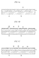
- FIGs. 1A, 1B, 1C, 1D, 1E, and 1F are sectional views illustrating a method of manufacturing an electron emission device according to an embodiment of the present invention;
- FIG. 2 is a photograph taken by a scanning electron microscope of the electron emission device manufactured according to the method depicted in FIGs. 1A through 1F;
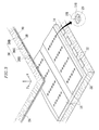
- FIG. 3 is a partial exploded perspective view of an electron emission display having the electron emission device manufactured according to the method depicted in FIGs. 1A through 1F;
- FIG. 4 is a partial sectional view of the electron emission display of FIGs. 1A through 1F;
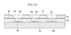
- FIGs. 5A, 5B, 5C, 5D, 5E, 5F, 5G, 5H, 5I, and 5J are sectional views illustrating a method of manufacturing an electron emission device according to another embodiment of the present invention;
- FIG. 6 is a partial exploded perspective view of an electron emission display having the electron emission device manufactured according to the method depicted in FIGs. 5A through 5J; and
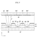
- FIG. 7 is a partial sectional view of the electron emission display of FIG. 6.
- In the following description, only certain exemplary embodiments of the present invention are shown and described, by way of illustration. As those skilled in the art would recognize, the described exemplary embodiments may be modified in various ways, all without departing from the spirit or scope of the present invention. Accordingly, the drawings and description are to be regarded as illustrative in nature, and not restrictive.
- Referring first to FIG. 1A, a conductive layer is formed on a
substrate 10 and processed to formfirst electrodes 12 having a stripe pattern. An insulating material is deposited on thesubstrate 10 to cover thefirst electrodes 12 to form aninsulating layer 14 having a certain (e.g., predetermined) thickness. The insulatinglayer 14 is formed by repeating screen-printing, drying and firing processes one or more times. The thickness of theinsulating layer 14 may be within a range of about 3-5 µm. - Another conductive layer is formed on the insulating
layer 14 and processed to formsecond electrodes 16 having a stripe pattern crossing thefirst electrodes 12 at right angles. Thefirst electrodes 12 may be formed of a transparent material such as indium tin oxide (ITO) while thesecond electrodes 16 may be formed of a metal material such as Chromium (Cr) or Molybdenum (Mo). - Referring to FIG. 1B, a
mask layer 18 is formed on thesubstrate 10 to cover the insulatinglayer 14 and thesecond electrodes 16 and is processed to haveopenings 181, each having a specific width (or diameter) D1. Themask layer 18 may be photoresist layer, and theopenings 181 in themask layer 18 may be formed by partial light exposing and developing processes. - Referring to FIG. 1C, the portions of the
second electrodes 16 exposed by theopenings 181 in themask layer 18 are removed using a first etching solution to formopenings 161. The width of each of theopenings 161 in thesecond electrodes 16 is identical to the width D1 of the corresponding opening in themask layer 18. - Referring to FIG. 1D, in a state where the
mask layer 18 is still maintained, to formopenings 141 in the insulatinglayer 14, portions of the insulatinglayer 14 exposed by theopenings 161 in thesecond electrodes 16 are removed using a second etching solution. - At this point, since the upper widths of the
openings 141 in the insulatinglayer 14 gradually increase as the etching depths increase due to the isotropic nature of the wet-etching process, the upper widths of theopenings 141 in the insulatinglayer 14, on which thesecond electrodes 16 are formed, become greater than those of each of the correspondingopenings 161 in thesecond electrodes 16. Therefore, portions of thesecond electrodes 16 may be suspended above theopenings 141 in the insulatinglayer 14, thereby decreasing shape stability and pattern preciseness. - Referring to FIG. 1E, the portions of the
second electrodes 16 suspended above theopenings 141 in the insulatinglayer 14 are removed through an etching process using the first etching solution. This etching process is performed by dipping the current substrate structure in the first etching solution. As a result, theopenings 141 in the insulatinglayer 14 are filled with the first etching solution. The suspended portions of thesecond electrodes 16 are thus removed by the etching solution that fills theopenings 141. - At this point, by controlling the dipping time of the substrate structure in the first etching solution, the widths of the
openings 161 in thesecond electrodes 16 can be adjusted. That is, when the dipping time is relatively long, the first etching solution permeates between themask layer 18 and the insulatinglayer 14 to etch theopenings 161 in thesecond electrodes 16 such that the widths of theopenings 161 in thesecond electrodes 16 are greater than those of the correspondingopenings 141 in the insulatinglayer 14. - In the above process, since portions of the
first electrodes 12 are exposed to the first etching solution, thefirst electrodes 12 are formed of a material different from that of thesecond electrodes 16. That is, thefirst electrodes 12 are formed of a material having a corrosion-resistance against the first etching solution so as not to be etched when thesecond electrodes 16 are etched. - Next, the
mask layer 18 is removed and, as shown in FIG. 1F,electron emission regions 20 are formed on the exposed portions of thefirst electrodes 12 through theopenings 141 in the insulatinglayer 14. - The
electron emission regions 20 may be formed of a material such as a carbonaceous material or a nanometer-sized material. For example, theelectron emission regions 20 can be formed of a material selected from the group consisting of carbon nanotubes, graphite, graphite nanofibers, diamonds, diamond-like carbon, C60, silicon nanowires, and combinations thereof. - The
electron emission regions 20 can be formed by preparing a paste mixture by mixing vehicles, binder and the like, screen-printing the paste mixture on the exposed portions of thefirst electrodes 12, and drying and firing the printed mixture. - The
first electrodes 12 may be cathode electrodes for applying electric current to theelectron emission regions 20 while thesecond electrodes 16 may be gate electrodes for inducing electron emission by forming an electric field around theelectron emission regions 20. - As described above, since the
second electrodes 16 are etched again after theopenings 141 of the insulatinglayer 14 are formed, no portion of thesecond electrodes 16 is suspended above theopenings 141 in the insulatinglayer 14. As a result, the shape stability of thesecond electrodes 16 can be improved and a short circuit between the first andsecond electrodes electron emission regions 20. - In addition, referring to FIGs 1A-1F, because only one
mask layer 18 is used, the process can be simplified and the sizes of theopenings 161 in thesecond electrodes 16 can be identical to theopenings 141 in the insulatinglayer 14. In addition, pattern preciseness of thesecond electrodes 16 is improved. Furthermore, by using the above-described method, theopenings - FIG. 2 shows a photograph taken by a scanning electron microscope of the electron emission device manufactured according to the method depicted in FIGs. 1A through 1F.
- In the electron emission device shown in FIG. 2, the distance between the center of the opening in the second electrode and the center of the opening in the insulating layer is less than 0.5 µm. Further the width (or diameter) of the opening in the second electrode is greater than that of the corresponding opening in the insulating layer. A gap between the upper circumference of the opening in the second electrode and the upper circumference of the corresponding opening in the insulating layer is less than 1 µm.
- Referring to FIGs. 3 and 4, an electron emission display according to an embodiment of the present invention manufactured by the above discussed method includes first and
second substrates second substrates - The
first electrodes 12 are formed on thefirst substrate 22 and the insulatinglayer 14 is formed on thefirst substrate 22 to fully cover thefirst electrodes 12. Thesecond electrodes 16 are formed on the insulatinglayer 14, crossing thefirst electrodes 12 at right angles. Theopenings layer 14 and thesecond electrodes 16 at each crossed region of the first andsecond electrodes electron emission regions 20. - At this point, the
openings second electrodes 16 and the insulatinglayer 14, respectively, using the above described method illustrated with reference to FIGs. 1A through 1F. Therefore, the distance between the center of each of theopenings 161 in thesecond electrodes 16 and the center of thecorresponding opening 141 in the insulatinglayer 14 is less than 0.5 µm. In addition, the gap between an upper circumference of each of theopenings 161 in thesecond electrode 16 and the upper circumference of thecorresponding opening 141 in the insulatinglayer 14 is less than 1 µm. - Phosphor layers 26 such as red (R), green (G) and blue (B) phosphor layers 26R, 26G and 26B are formed on a surface of the
second substrate 24 opposite to thefirst substrate 22, andblack layers 28 are arranged between the phosphor layers 26. Each crossed region of the first andsecond electrodes - An
anode electrode 30 is formed of a conductive material, such as aluminum, and is formed on the phosphor andblack layers anode electrode 30 increases the screen luminance by receiving the high voltage required to accelerate the electron beams traveling from thefirst substrate 22 toward thesecond substrate 24 and by reflecting the visible light rays radiated from thephosphor layer 26, toward thefirst substrate 22 to thesecond substrate 24, thereby increasing the screen's luminance. - Disposed between the first and
second substrates second substrates black layers 28 and do not trespass onto the phosphor layers 26. - The above-described electron emission display is driven when a certain (e.g., predetermined) voltage is applied to the first, second and
anode electrodes - For example, referring to FIG. 4, one of the first and
second electrodes anode electrode 30 receives a DC voltage capable of accelerating the electron beams (e.g., a DC voltage of hundreds through thousands of volts). - Electric fields are formed around the
electron emission regions 20 of pixels where a voltage difference between the first andsecond electrodes electron emission regions 20. The high voltage applied to theanode electrode 30 causes the emitted electrons to strike the phosphor layers 26 of the corresponding pixel, thereby exciting the phosphor layers 26. - Referring to FIG. 5A, a conductive layer is formed on a
substrate 34 and processed to formfirst electrodes 36 having a stripe pattern. An insulating material is deposited on thesubstrate 34 to cover thefirst electrodes 36 to form a first insulatinglayer 38. - Another conductive layer is formed on the first insulating
layer 38 and processed to formsecond electrodes 40 having a stripe pattern crossing thefirst electrodes 36 at right angles. Another insulating material is deposited on the first insulatinglayer 38 to cover thesecond electrodes 40 to form a second insulatinglayer 42. Another conductive layer is formed on the second insulatinglayer 42 to form athird electrode 44. - Referring to FIG. 5B, a
second mask layer 46 is formed on thethird electrode 44 and processed to formopenings 461, each having a width (or diameter) D2. - Referring to FIG. 5C, portions of the
third electrode 44 exposed by theopenings 461 in thesecond mask layer 46 are removed using a third etching solution to formopenings 441. The width (or diameter) of each opening 441 in thethird electrode 44 is identical to the width (or diameter) D2 of theopenings 461 in thesecond mask layer 46. - Referring to FIG. 5D, in a state where the
second mask layer 46 is still maintained, portions of the second insulatinglayer 42 exposed by theopenings 441 in thethird electrode 44 are removed using a fourth etching solution to formopenings 421. At this point, since the upper widths of theopenings 421 in the second insulatinglayer 42 gradually increase as the etching depths increase due to the isotropic nature of the wet-etching process, the upper width of each of theopenings 421 in the second insulatinglayer 42, on which thethird electrode 44 is formed, becomes greater than that of thecorresponding opening 441 in thethird electrode 44. Therefore, a portion of thethird electrode 44 may be suspended above theopenings 421 in the second insulatinglayer 42, thereby decreasing shape stability and pattern preciseness. - Referring to FIG. 5E, the suspended portions of the
third electrodes 44 above theopenings 421 are removed through an etching process using the third etching solution. This etching process is performed by dipping the current substrate structure in the third etching solution. Then, theopenings 421 in the second insulatinglayer 42 are filled with the third etching solution, and thus, the suspended portions of thethird electrodes 44 are removed by the third etching solution filled in theopenings 421. Therefore, the widths (or diameters) of theopenings 441 in thethird electrode 44 are precisely formed to be equal to or greater than those of the correspondingopenings 421 in the second insulatinglayer 42. Thisthird electrode 44 functions as a focusing electrode for focusing electron beams. - In the above process, since portions of the
second electrodes 40 are exposed to the third etching solution, thesecond electrodes 40 are formed of a material different from that of thethird electrodes 44. That is, thesecond electrodes 40 are formed of a material having a corrosion-resistance against the third etching solution so as not to be etched when thethird electrodes 44 are etched. - Next, the
second mask layer 46 is removed and, referring to FIG. 5F, afirst mask layer 48 is formed on thesubstrate 34 and processed to formopenings 481 each having a width (or diameter) D3 and exposing a portion of thesecond electrodes 40. - Referring to FIG. 5G, the portions of the
second electrodes 40 exposed by theopenings 481 in thefirst mask layer 48 are removed by the first etching solution to formopenings 401. The width (or diameter) of each of theopenings 401 is identical to that of thecorresponding opening 481 in thefirst mask layer 48. At this point, the widths of theopenings 481 in thefirst mask layer 48 and the widths of theopenings 401 in thesecond electrodes 40 may be smaller than the lower widths of theopenings 421 in the second insulatinglayer 42. - Referring to FIG. 5H, in a state where the
first mask layer 48 is still maintained, the portions of the first insulatinglayer 38 exposed by theopenings 401 in thesecond electrodes 40 are removed by the second etching solution to formopenings 381. Likewise, at this point, since the upper widths (or diameters) of theopenings 381 in the first insulatinglayer 38 gradually increase as the depths increase due to the isotropic nature of the wet-etching process, the upper width (or diameter) of each of theopenings 381 in the first insulatinglayer 38, on which thesecond electrodes 40 are formed, becomes greater than that of thecorresponding opening 401 in thesecond electrodes 40. - Referring to FIG. 51, the current substrate structure is dipped in the first etching solution to remove the portions of the
second electrodes 40 exposed to theopenings 381 in the first insulatinglayer 38. By this secondary etching process for thesecond electrodes 40, the widths (or diameters) of theopenings 401 in thesecond electrodes 40 are precisely formed to be equal to or greater than those of theopenings 381 in the first insulatinglayer 38. - In the above process, since portions of the
first electrodes 36 are exposed to the first etching solution, thefirst electrodes 36 can be formed of a material different from that of thesecond electrodes 40. That is, thefirst electrodes 36 can be formed of a material having a corrosion-resistance against the first etching solution so as not to be etched when thesecond electrodes 40 are etched. - According to a preferred embodiment of the invention, the second etching solution may be the same as the fourth etching solution, but the invention is not limited thereto.
- Next, the
first mask layer 48 is removed and, referring now to FIG. 5J,electron emission regions 50 are formed on thefirst electrodes 36 through theopenings 381 in the first insulatinglayer 38. The material and manufacturing method of theelectron emission regions 50 are identical to those of the foregoing embodiment. - According to this embodiment, since the
third electrodes 44 are secondarily etched after theopenings 421 in the second insulatinglayer 42 are formed and thesecond electrodes 40 are secondarily etched after theopenings 381 in the first insulatinglayer 38 are formed, the shape stability of the third andsecond electrodes openings - FIGs. 6 and 7 show an electron emission display having the electron emission device manufactured according to the method illustrated with reference to FIGs. 5A through 5J.
- An electron emission display according to this embodiment of the present invention includes first and second substrates 22' and 24' facing each other and spaced apart by a certain (e.g., predetermined) distance. A sealing member (not shown) is provided at the peripheries of the first and the second substrates 22' and 24' to seal them together.
- The first insulating
layer 38 is formed on the first substrate 22' to cover thefirst electrodes 36 and the second insulatinglayer 42 is formed on the first insulatinglayer 38 to cover thesecond electrodes 40. Thethird electrode 44 is formed on the second insulatinglayer 42. - One
opening 441 is formed on thethird electrode 44 at each crossed region of the first andsecond electrodes third electrode 44 to correspond to oneelectron emission region 50 to individually focus the electrons emitted from oneelectron emission region 50. The former is applied to this embodiment. - The
third electrode 44 receives 0V or a negative DC voltage of several to tens of volts. Therefore, thethird electrode 44 converges the electrons to a central portion of bunched electron beams by applying repulsive force to the electrons. - As the method depicted in FIGs. 1A through 1J is applied to manufacture the electron emission display, the distance between the center of each of the
openings 441 in thethird electrode 44 and the center of thecorresponding opening 421 in the second insulatinglayer 42 is less than 0.5 µm. That is, the centers of theopenings openings 401 in thesecond electrodes 40 and the center of thecorresponding opening 381 in the first insulatinglayer 38 is also less than 0.5 µm. That is, the centers of theopenings - In addition, the gap between the upper circumference of each of the
openings 441 in thethird electrode 441 and the upper circumference of thecorresponding opening 421 in the second insulatinglayer 42 is less than 1 µm. The gap between the upper circumference of each of theopenings 401 in thesecond electrodes 40 and the upper circumference of thecorresponding opening 381 in the first insulatinglayer 38 is also less than 1 µm.
Claims (20)
- A method of manufacturing an electron emission device comprising at least one first electrode (12, 36) disposed on a first substrate (10, 34), at least one electron emission region (20, 50) disposed on the at least one first electrode (12, 36), and at least one second electrode (16, 40) disposed on the at least one first electrode (12, 36) with an insulating layer (14, 38) interposed between the at least one first electrode (12, 36) and the at least one second electrode (16, 40), the insulating layer (14, 38) and the at least one second electrode (16, 40) having respective openings (141, 161) for exposing the at least one electron emission region (20, 50), the method comprising:providing the substrate (10, 34), forming the at least one first electrode (12, 36) on the substrate (10, 34), forming the insulating layer (14, 38) and forming the at least one second electrode (16, 40) over the insulating layer (14, 38);forming a mask layer (18, 48) having an opening (181, 481) on the second electrode (16, 40);forming the opening (161, 401) in the second electrode (16, 40) by etching the second electrode (16, 40) using the mask layer (18, 48);forming the opening (141, 381) in the insulating layer (14, 38) by wet-etching the insulating layer (14, 38) such that a width of an upper portion of the opening (141, 381) in the insulating layer (14, 38) is greater than a width of the opening (161, 401) in the second electrode (16, 40);enlarging the opening (161, 401) in the second electrode (16, 40) by etching an exposed portion of the second electrode (16, 40) exposed to the opening (141, 381) in the insulating layer (14, 38); andremoving the mask layer (18, 48).
- The method of claim 1, wherein the mask layer (18) is directly applied onto the second electrode (16).
- The method according to one of the preceding claims, wherein a first etching solution is used for forming the opening (161, 401) in the second electrode, and a second etching solution is used for forming the opening (141, 381) in the insulating layer (14, 38), wherein the first etching solution is different from the second etching solution.
- The method according to claim 3, wherein the etching of the exposed portion of the second electrode (16, 40) is a wet-etching performed by filling the opening (141, 381) in the insulating layer (14, 38) with the first etching solution used for etching the second electrode (16, 40).
- The method according to one of the preceding claims, wherein the opening (161, 401) in the second electrode (16, 40) is enlarged by etching the exposed portion of the second electrode (16, 40) such that the width of the opening (161, 401) in the second electrode (16, 40) is greater than the width of the upper portion of the opening (141, 381) in the insulating layer (14, 38).
- The method according to one of the preceding claims, wherein the first electrode (12, 36) is formed of a conductive material having a corrosion-resistance against the first etching solution.
- The method according to one of the preceding claims, wherein the steps of etching the insulating layer (14, 38) and etching the second electrode (16, 40) are controlled such that the distance between the center of the opening (141, 381) in the insulating layer (14, 38) and the center of the corresponding opening (161, 401) in the second electrode (16, 40) is less than 0.5 µm.
- The method according to one of the preceding claims, wherein the steps of etching the insulating layer (14, 38) and etching the second electrode (16, 40) are controlled such that the opening (161, 401) in the second electrode (16, 40) has a width greater than that of the opening (141, 381) in the insulating layer (14, 38) and the gap between an upper circumference of the opening (161, 401) in the second electrode (16, 40) and an upper circumference of the opening (141, 381) in the insulating layer (14, 38) is less than 1 µm.
- The method according to one of the preceding claims, further comprising, after the removing of the mask layer (18, 48), forming the electron emission region (20, 50) on the first electrode (12, 36), wherein the electron emission region (20, 50) is formed of a material selected from the group consisting of carbon nanotubes, graphite, graphite nanofibers, diamonds, diamond-like carbon, C60, silicon nanowires, and combinations thereof.
- The method according to one of the claims 1 and 3-9, further comprising prior to the formation of the mask layer (48):forming a third electrode (44) on the second electrode (40) with a second insulating layer (42) interposed between the second electrode (40) and the third electrode (44);forming a second mask layer (46) having an opening (461) on the third electrode (44);forming an opening (441) in the third electrode (44) by etching the third electrode (44) using the second mask layer (46);forming an opening (421) in the second insulating layer (42) by wet-etching the second insulating layer (42) such that a width of an upper portion of the opening (421) in the second insulating layer (42) is greater than a width of the opening (441) in the third electrode (44);enlarging the opening (441) in the third electrode (44) by etching an exposed portion of the third electrode (44) exposed to the opening (421) in the second insulating layer (42); andremoving the second mask layer (46).
- The method of claim 10, wherein the mask layer (48) is directly applied onto the second electrode (40), the third electrode (44) and the second insulating layer (42).
- The method according to one of the claims 10 and 11, wherein a third etching solution is used for forming the opening (441) in the third electrode (44), and a fourth etching solution is used for forming the opening (421) in the second insulating layer (42), wherein the third etching solution is different from the fourth etching solution.
- The method of claim 12, wherein the etching of the exposed portion of the third electrode (44) is a wet-etching performed by filling the opening (421) in the second insulating layer (42) with the third etching solution for etching the third electrode (44).
- The method according to one of the claims 10 - 13, wherein the opening (441) in the third electrode (44) is enlarged by etching the exposed portion of the third electrode (44) such that a width of the opening (441) in the third electrode (44) is greater than a width of the opening (421) in the second insulating layer (42).
- The method according to one of the claims 10-14, wherein the second electrode (40) is formed of a conductive material having a corrosion-resistance against the third etching solution.
- An electron emission device comprising:a first substrate (10, 34);a first electrode (12, 36) disposed on the first substrate (10, 34);an electron emission region (20, 50) disposed on the first electrode (12, 36); anda second electrode (16, 40) disposed on the first electrode (12, 36) with an insulating layer (14, 38) interposed between the first electrode (12, 36) and the second electrode (16, 40);wherein the insulating layer (14, 38) and the second electrode (16, 40) have respective openings (141, 161) for exposing the electron emission region (20, 50); andwherein the distance between the center of an opening (141, 381) in the insulating layer (14, 38) and the center of a corresponding opening (161, 401) in the second electrode (16, 40) is less than 0.5 µm.
- The electron emission device of claim 16, wherein the opening (161, 401) in the second electrode (16, 40) has a width greater than that of the opening (141, 381) in the insulating layer (14, 38) and the gap between the upper circumference of the opening (161, 401) in the second electrode (16, 40) and the upper circumference of the corresponding opening (141, 381) in the insulating layer (14, 38) is less than 1 µm.
- The electron emission device according to one of claims 16 and 17, further comprising:a third electrode (44) disposed on the second electrode (40) with a second insulating layer (42) interposed between the second electrode (40) and third electrode (44);wherein the first insulating layer (38), the second electrode (40), the second insulating layer (42), and the third electrode (44) have respective openings (381, 401, 421, 441) for exposing the electron emission region (50); andwherein the distance between the center of an opening (421) in the second insulating layer (42) and the center of a corresponding opening (441) in the third electrode (44) is less than 0.5 µm.
- The electron emission device of claim 18, wherein the opening (441) in the third electrode (44) has a width greater than a width of the opening (421) in the second insulating layer (42) and the gap between the upper circumference of the opening (441) in the third electrode (44) and the upper circumference of the corresponding opening (421) in the second insulating layer (42) is less than 1 µm.
- An electron emission display, comprising:an electron emission device according to one of the claims 16-19;a second substrate (24) facing the first substrate (22) with a vacuum region formed between the first and second substrates (22, 24);phosphor layers (26, 26') disposed on a surface of the second substrate (24) facing the first substrate (22); andan anode electrode (30, 30') disposed on the phosphor layers (26, 26').
Applications Claiming Priority (1)
| Application Number | Priority Date | Filing Date | Title |
|---|---|---|---|
| KR1020060026524A KR20070096319A (en) | 2006-03-23 | 2006-03-23 | Electron emitting device, manufacturing method thereof and electron emitting display device using same |
Publications (1)
| Publication Number | Publication Date |
|---|---|
| EP1843378A1 true EP1843378A1 (en) | 2007-10-10 |
Family
ID=38294283
Family Applications (1)
| Application Number | Title | Priority Date | Filing Date |
|---|---|---|---|
| EP07104536A Withdrawn EP1843378A1 (en) | 2006-03-23 | 2007-03-21 | Electron emission device, method of manufacturing the electron emission device, and electron emission display using the electron emission device |
Country Status (5)
| Country | Link |
|---|---|
| US (1) | US20070221624A1 (en) |
| EP (1) | EP1843378A1 (en) |
| JP (1) | JP2007258167A (en) |
| KR (1) | KR20070096319A (en) |
| CN (1) | CN101042972A (en) |
Citations (3)
| Publication number | Priority date | Publication date | Assignee | Title |
|---|---|---|---|---|
| US6210246B1 (en) * | 1998-05-26 | 2001-04-03 | Commissariat A L'energie Atomique | Method for making an electron source with microtips, with self-aligned focusing grid |
| KR20030080767A (en) * | 2002-04-10 | 2003-10-17 | 삼성에스디아이 주식회사 | Method for fabricating negative hole and field emission display with the hole |
| EP1630844A2 (en) * | 2004-08-30 | 2006-03-01 | Samsung SDI Co., Ltd. | Electron emission device and manufacturing method thereof |
-
2006
- 2006-03-23 KR KR1020060026524A patent/KR20070096319A/en not_active Withdrawn
-
2007
- 2007-02-23 JP JP2007044433A patent/JP2007258167A/en active Pending
- 2007-03-14 US US11/686,316 patent/US20070221624A1/en not_active Abandoned
- 2007-03-19 CN CNA2007100874848A patent/CN101042972A/en active Pending
- 2007-03-21 EP EP07104536A patent/EP1843378A1/en not_active Withdrawn
Patent Citations (3)
| Publication number | Priority date | Publication date | Assignee | Title |
|---|---|---|---|---|
| US6210246B1 (en) * | 1998-05-26 | 2001-04-03 | Commissariat A L'energie Atomique | Method for making an electron source with microtips, with self-aligned focusing grid |
| KR20030080767A (en) * | 2002-04-10 | 2003-10-17 | 삼성에스디아이 주식회사 | Method for fabricating negative hole and field emission display with the hole |
| EP1630844A2 (en) * | 2004-08-30 | 2006-03-01 | Samsung SDI Co., Ltd. | Electron emission device and manufacturing method thereof |
Non-Patent Citations (3)
| Title |
|---|
| BAE SUNGIL ET AL: "Self-aligned cathodes in recessed geometry for reduced gate currents in nanostructured carbon triodes", JOURNAL OF VACUUM SCIENCE AND TECHNOLOGY. B, MICROELECTRONICS AND NANOMETER STRUCTURES PROCESSING, MEASUREMENT AND PHENOMENA, AMERICAN INSTITUTE OF PHYSICS, NEW YORK, NY, US, vol. 24, no. 1, 10 January 2006 (2006-01-10), pages 59 - 63, XP012091332, ISSN: 1071-1023 * |
| KANG W P ET AL: "Diamond and carbon-derived vacuum micro- and nano-electronic devices", DIAMOND AND RELATED MATERIALS, ELSEVIER SCIENCE PUBLISHERS, AMSTERDAM, NL, vol. 14, no. 3-7, March 2005 (2005-03-01), pages 685 - 691, XP004857146, ISSN: 0925-9635 * |
| SEO WOO JONG ET AL: "Fabrication of low-gate-current triode field emitters with planar carbon nanoparticle cathodes", JOURNAL OF VACUUM SCIENCE & TECHNOLOGY B: MICROELECTRONICS PROCESSING AND PHENOMENA, AMERICAN VACUUM SOCIETY, NEW YORK, NY, US, vol. 22, no. 3, May 2004 (2004-05-01), pages 1294 - 1297, XP012074417, ISSN: 0734-211X * |
Also Published As
| Publication number | Publication date |
|---|---|
| JP2007258167A (en) | 2007-10-04 |
| US20070221624A1 (en) | 2007-09-27 |
| CN101042972A (en) | 2007-09-26 |
| KR20070096319A (en) | 2007-10-02 |
Similar Documents
| Publication | Publication Date | Title |
|---|---|---|
| US7156715B2 (en) | Triode structure of field emission display and fabrication method thereof | |
| US6116975A (en) | Field emission cathode manufacturing method | |
| EP1115134B1 (en) | Field emission device and method for fabricating the same | |
| US20050152042A1 (en) | Fiber based field emitter display | |
| US20060261725A1 (en) | Electron emission device, electron emission display, and manufacturing method of the electron emission device | |
| KR101009983B1 (en) | Electron emission display device | |
| US7710014B2 (en) | Electron emission device, electron emission display device using the same and method of manufacturing the same | |
| JP2006049287A (en) | Electron emitting device and manufacturing method thereof | |
| US7612493B2 (en) | Electron emission device with improved focusing of electron beams | |
| US20060022577A1 (en) | Electron emission device and method for manufacturing | |
| KR20010062703A (en) | Field emission cathode, electron emission device and electron emission device manufacturing method | |
| EP1630844A2 (en) | Electron emission device and manufacturing method thereof | |
| US20070221624A1 (en) | Electron emission device, method of manufacturing the electron emission device, and electron emission display using the electron emission device | |
| KR950008757B1 (en) | Field emission device and manufacture method | |
| EP1758147A2 (en) | Electron emission element, electron emission display, and method of manufacturing electron emission unit for the electron emission display | |
| US20080116794A1 (en) | Electron emission device and light emission device having the electron emission device | |
| EP1821330B1 (en) | Electron emission device and electron emission display using the same | |
| EP1630843B1 (en) | Electron emission device and method of manufacturing the same | |
| US20070120462A1 (en) | Electron emission device, method of manufacturing the electron emission device, and electron emission display having the electron emission device | |
| KR100357832B1 (en) | Method of Fabricating Focusing Device in Field Emission Display | |
| KR940005883B1 (en) | Field emission display device having improved cathode | |
| KR20070043391A (en) | Electron emitting device, electron emitting display device using same and manufacturing method thereof | |
| KR20070056614A (en) | Method of manufacturing an electron emitting device | |
| JP2000195448A (en) | Flat display device and method of manufacturing field emission type cathode | |
| KR20070043392A (en) | Electron emitting device, electron emitting display device using same and manufacturing method thereof |
Legal Events
| Date | Code | Title | Description |
|---|---|---|---|
| PUAI | Public reference made under article 153(3) epc to a published international application that has entered the european phase |
Free format text: ORIGINAL CODE: 0009012 |
|
| 17P | Request for examination filed |
Effective date: 20070321 |
|
| AK | Designated contracting states |
Kind code of ref document: A1 Designated state(s): AT BE BG CH CY CZ DE DK EE ES FI FR GB GR HU IE IS IT LI LT LU LV MC MT NL PL PT RO SE SI SK TR |
|
| AX | Request for extension of the european patent |
Extension state: AL BA HR MK YU |
|
| STAA | Information on the status of an ep patent application or granted ep patent |
Free format text: STATUS: THE APPLICATION HAS BEEN WITHDRAWN |
|
| RIN1 | Information on inventor provided before grant (corrected) |
Inventor name: HONG, SU-BONGSAMSUNG SDI CO., LTD. Inventor name: CHO, JIN-HUISAMSUNG SDI CO., LTD. Inventor name: JEON, SANG-HOSAMSUNG SDI CO., LTD. Inventor name: JEA, BYUNG-GILSAMSUNG SDI CO., LTD. Inventor name: LEE, SANG-JOSAMSUNG SDI CO., LTD. Inventor name: AHN, SANG-HYUCKSAMSUNG SDI CO., LTD. |
|
| 18W | Application withdrawn |
Effective date: 20071122 |