EP1842940A1 - Method for forming a group III nitride material on a silicon substrate - Google Patents
Method for forming a group III nitride material on a silicon substrate Download PDFInfo
- Publication number
- EP1842940A1 EP1842940A1 EP06118018A EP06118018A EP1842940A1 EP 1842940 A1 EP1842940 A1 EP 1842940A1 EP 06118018 A EP06118018 A EP 06118018A EP 06118018 A EP06118018 A EP 06118018A EP 1842940 A1 EP1842940 A1 EP 1842940A1
- Authority
- EP
- European Patent Office
- Prior art keywords
- layer
- iii nitride
- group iii
- sic
- reactor
- Prior art date
- Legal status (The legal status is an assumption and is not a legal conclusion. Google has not performed a legal analysis and makes no representation as to the accuracy of the status listed.)
- Withdrawn
Links
Images



Classifications
-
- C—CHEMISTRY; METALLURGY
- C30—CRYSTAL GROWTH
- C30B—SINGLE-CRYSTAL GROWTH; UNIDIRECTIONAL SOLIDIFICATION OF EUTECTIC MATERIAL OR UNIDIRECTIONAL DEMIXING OF EUTECTOID MATERIAL; REFINING BY ZONE-MELTING OF MATERIAL; PRODUCTION OF A HOMOGENEOUS POLYCRYSTALLINE MATERIAL WITH DEFINED STRUCTURE; SINGLE CRYSTALS OR HOMOGENEOUS POLYCRYSTALLINE MATERIAL WITH DEFINED STRUCTURE; AFTER-TREATMENT OF SINGLE CRYSTALS OR A HOMOGENEOUS POLYCRYSTALLINE MATERIAL WITH DEFINED STRUCTURE; APPARATUS THEREFOR
- C30B29/00—Single crystals or homogeneous polycrystalline material with defined structure characterised by the material or by their shape
- C30B29/10—Inorganic compounds or compositions
- C30B29/40—AIIIBV compounds wherein A is B, Al, Ga, In or Tl and B is N, P, As, Sb or Bi
- C30B29/403—AIII-nitrides
-
- C—CHEMISTRY; METALLURGY
- C23—COATING METALLIC MATERIAL; COATING MATERIAL WITH METALLIC MATERIAL; CHEMICAL SURFACE TREATMENT; DIFFUSION TREATMENT OF METALLIC MATERIAL; COATING BY VACUUM EVAPORATION, BY SPUTTERING, BY ION IMPLANTATION OR BY CHEMICAL VAPOUR DEPOSITION, IN GENERAL; INHIBITING CORROSION OF METALLIC MATERIAL OR INCRUSTATION IN GENERAL
- C23C—COATING METALLIC MATERIAL; COATING MATERIAL WITH METALLIC MATERIAL; SURFACE TREATMENT OF METALLIC MATERIAL BY DIFFUSION INTO THE SURFACE, BY CHEMICAL CONVERSION OR SUBSTITUTION; COATING BY VACUUM EVAPORATION, BY SPUTTERING, BY ION IMPLANTATION OR BY CHEMICAL VAPOUR DEPOSITION, IN GENERAL
- C23C16/00—Chemical coating by decomposition of gaseous compounds, without leaving reaction products of surface material in the coating, i.e. chemical vapour deposition [CVD] processes
- C23C16/02—Pretreatment of the material to be coated
- C23C16/0272—Deposition of sub-layers, e.g. to promote the adhesion of the main coating
-
- C—CHEMISTRY; METALLURGY
- C23—COATING METALLIC MATERIAL; COATING MATERIAL WITH METALLIC MATERIAL; CHEMICAL SURFACE TREATMENT; DIFFUSION TREATMENT OF METALLIC MATERIAL; COATING BY VACUUM EVAPORATION, BY SPUTTERING, BY ION IMPLANTATION OR BY CHEMICAL VAPOUR DEPOSITION, IN GENERAL; INHIBITING CORROSION OF METALLIC MATERIAL OR INCRUSTATION IN GENERAL
- C23C—COATING METALLIC MATERIAL; COATING MATERIAL WITH METALLIC MATERIAL; SURFACE TREATMENT OF METALLIC MATERIAL BY DIFFUSION INTO THE SURFACE, BY CHEMICAL CONVERSION OR SUBSTITUTION; COATING BY VACUUM EVAPORATION, BY SPUTTERING, BY ION IMPLANTATION OR BY CHEMICAL VAPOUR DEPOSITION, IN GENERAL
- C23C16/00—Chemical coating by decomposition of gaseous compounds, without leaving reaction products of surface material in the coating, i.e. chemical vapour deposition [CVD] processes
- C23C16/22—Chemical coating by decomposition of gaseous compounds, without leaving reaction products of surface material in the coating, i.e. chemical vapour deposition [CVD] processes characterised by the deposition of inorganic material, other than metallic material
- C23C16/30—Deposition of compounds, mixtures or solid solutions, e.g. borides, carbides, nitrides
- C23C16/301—AIII BV compounds, where A is Al, Ga, In or Tl and B is N, P, As, Sb or Bi
- C23C16/303—Nitrides
-
- C—CHEMISTRY; METALLURGY
- C23—COATING METALLIC MATERIAL; COATING MATERIAL WITH METALLIC MATERIAL; CHEMICAL SURFACE TREATMENT; DIFFUSION TREATMENT OF METALLIC MATERIAL; COATING BY VACUUM EVAPORATION, BY SPUTTERING, BY ION IMPLANTATION OR BY CHEMICAL VAPOUR DEPOSITION, IN GENERAL; INHIBITING CORROSION OF METALLIC MATERIAL OR INCRUSTATION IN GENERAL
- C23C—COATING METALLIC MATERIAL; COATING MATERIAL WITH METALLIC MATERIAL; SURFACE TREATMENT OF METALLIC MATERIAL BY DIFFUSION INTO THE SURFACE, BY CHEMICAL CONVERSION OR SUBSTITUTION; COATING BY VACUUM EVAPORATION, BY SPUTTERING, BY ION IMPLANTATION OR BY CHEMICAL VAPOUR DEPOSITION, IN GENERAL
- C23C16/00—Chemical coating by decomposition of gaseous compounds, without leaving reaction products of surface material in the coating, i.e. chemical vapour deposition [CVD] processes
- C23C16/22—Chemical coating by decomposition of gaseous compounds, without leaving reaction products of surface material in the coating, i.e. chemical vapour deposition [CVD] processes characterised by the deposition of inorganic material, other than metallic material
- C23C16/30—Deposition of compounds, mixtures or solid solutions, e.g. borides, carbides, nitrides
- C23C16/32—Carbides
- C23C16/325—Silicon carbide
-
- C—CHEMISTRY; METALLURGY
- C23—COATING METALLIC MATERIAL; COATING MATERIAL WITH METALLIC MATERIAL; CHEMICAL SURFACE TREATMENT; DIFFUSION TREATMENT OF METALLIC MATERIAL; COATING BY VACUUM EVAPORATION, BY SPUTTERING, BY ION IMPLANTATION OR BY CHEMICAL VAPOUR DEPOSITION, IN GENERAL; INHIBITING CORROSION OF METALLIC MATERIAL OR INCRUSTATION IN GENERAL
- C23C—COATING METALLIC MATERIAL; COATING MATERIAL WITH METALLIC MATERIAL; SURFACE TREATMENT OF METALLIC MATERIAL BY DIFFUSION INTO THE SURFACE, BY CHEMICAL CONVERSION OR SUBSTITUTION; COATING BY VACUUM EVAPORATION, BY SPUTTERING, BY ION IMPLANTATION OR BY CHEMICAL VAPOUR DEPOSITION, IN GENERAL
- C23C16/00—Chemical coating by decomposition of gaseous compounds, without leaving reaction products of surface material in the coating, i.e. chemical vapour deposition [CVD] processes
- C23C16/44—Chemical coating by decomposition of gaseous compounds, without leaving reaction products of surface material in the coating, i.e. chemical vapour deposition [CVD] processes characterised by the method of coating
- C23C16/455—Chemical coating by decomposition of gaseous compounds, without leaving reaction products of surface material in the coating, i.e. chemical vapour deposition [CVD] processes characterised by the method of coating characterised by the method used for introducing gases into reaction chamber or for modifying gas flows in reaction chamber
- C23C16/45523—Pulsed gas flow or change of composition over time
-
- C—CHEMISTRY; METALLURGY
- C30—CRYSTAL GROWTH
- C30B—SINGLE-CRYSTAL GROWTH; UNIDIRECTIONAL SOLIDIFICATION OF EUTECTIC MATERIAL OR UNIDIRECTIONAL DEMIXING OF EUTECTOID MATERIAL; REFINING BY ZONE-MELTING OF MATERIAL; PRODUCTION OF A HOMOGENEOUS POLYCRYSTALLINE MATERIAL WITH DEFINED STRUCTURE; SINGLE CRYSTALS OR HOMOGENEOUS POLYCRYSTALLINE MATERIAL WITH DEFINED STRUCTURE; AFTER-TREATMENT OF SINGLE CRYSTALS OR A HOMOGENEOUS POLYCRYSTALLINE MATERIAL WITH DEFINED STRUCTURE; APPARATUS THEREFOR
- C30B25/00—Single-crystal growth by chemical reaction of reactive gases, e.g. chemical vapour-deposition growth
- C30B25/02—Epitaxial-layer growth
-
- C—CHEMISTRY; METALLURGY
- C30—CRYSTAL GROWTH
- C30B—SINGLE-CRYSTAL GROWTH; UNIDIRECTIONAL SOLIDIFICATION OF EUTECTIC MATERIAL OR UNIDIRECTIONAL DEMIXING OF EUTECTOID MATERIAL; REFINING BY ZONE-MELTING OF MATERIAL; PRODUCTION OF A HOMOGENEOUS POLYCRYSTALLINE MATERIAL WITH DEFINED STRUCTURE; SINGLE CRYSTALS OR HOMOGENEOUS POLYCRYSTALLINE MATERIAL WITH DEFINED STRUCTURE; AFTER-TREATMENT OF SINGLE CRYSTALS OR A HOMOGENEOUS POLYCRYSTALLINE MATERIAL WITH DEFINED STRUCTURE; APPARATUS THEREFOR
- C30B25/00—Single-crystal growth by chemical reaction of reactive gases, e.g. chemical vapour-deposition growth
- C30B25/02—Epitaxial-layer growth
- C30B25/18—Epitaxial-layer growth characterised by the substrate
-
- C—CHEMISTRY; METALLURGY
- C30—CRYSTAL GROWTH
- C30B—SINGLE-CRYSTAL GROWTH; UNIDIRECTIONAL SOLIDIFICATION OF EUTECTIC MATERIAL OR UNIDIRECTIONAL DEMIXING OF EUTECTOID MATERIAL; REFINING BY ZONE-MELTING OF MATERIAL; PRODUCTION OF A HOMOGENEOUS POLYCRYSTALLINE MATERIAL WITH DEFINED STRUCTURE; SINGLE CRYSTALS OR HOMOGENEOUS POLYCRYSTALLINE MATERIAL WITH DEFINED STRUCTURE; AFTER-TREATMENT OF SINGLE CRYSTALS OR A HOMOGENEOUS POLYCRYSTALLINE MATERIAL WITH DEFINED STRUCTURE; APPARATUS THEREFOR
- C30B29/00—Single crystals or homogeneous polycrystalline material with defined structure characterised by the material or by their shape
- C30B29/10—Inorganic compounds or compositions
- C30B29/36—Carbides
-
- H—ELECTRICITY
- H10—SEMICONDUCTOR DEVICES; ELECTRIC SOLID-STATE DEVICES NOT OTHERWISE PROVIDED FOR
- H10P—GENERIC PROCESSES OR APPARATUS FOR THE MANUFACTURE OR TREATMENT OF DEVICES COVERED BY CLASS H10
- H10P14/00—Formation of materials, e.g. in the shape of layers or pillars
- H10P14/20—Formation of materials, e.g. in the shape of layers or pillars of semiconductor materials
- H10P14/24—Formation of materials, e.g. in the shape of layers or pillars of semiconductor materials using chemical vapour deposition [CVD]
-
- H—ELECTRICITY
- H10—SEMICONDUCTOR DEVICES; ELECTRIC SOLID-STATE DEVICES NOT OTHERWISE PROVIDED FOR
- H10P—GENERIC PROCESSES OR APPARATUS FOR THE MANUFACTURE OR TREATMENT OF DEVICES COVERED BY CLASS H10
- H10P14/00—Formation of materials, e.g. in the shape of layers or pillars
- H10P14/20—Formation of materials, e.g. in the shape of layers or pillars of semiconductor materials
- H10P14/29—Formation of materials, e.g. in the shape of layers or pillars of semiconductor materials characterised by the substrates
- H10P14/2901—Materials
- H10P14/2902—Materials being Group IVA materials
- H10P14/2905—Silicon, silicon germanium or germanium
-
- H—ELECTRICITY
- H10—SEMICONDUCTOR DEVICES; ELECTRIC SOLID-STATE DEVICES NOT OTHERWISE PROVIDED FOR
- H10P—GENERIC PROCESSES OR APPARATUS FOR THE MANUFACTURE OR TREATMENT OF DEVICES COVERED BY CLASS H10
- H10P14/00—Formation of materials, e.g. in the shape of layers or pillars
- H10P14/20—Formation of materials, e.g. in the shape of layers or pillars of semiconductor materials
- H10P14/32—Formation of materials, e.g. in the shape of layers or pillars of semiconductor materials characterised by intermediate layers between substrates and deposited layers
- H10P14/3202—Materials thereof
- H10P14/3204—Materials thereof being Group IVA semiconducting materials
- H10P14/3208—Silicon carbide
-
- H—ELECTRICITY
- H10—SEMICONDUCTOR DEVICES; ELECTRIC SOLID-STATE DEVICES NOT OTHERWISE PROVIDED FOR
- H10P—GENERIC PROCESSES OR APPARATUS FOR THE MANUFACTURE OR TREATMENT OF DEVICES COVERED BY CLASS H10
- H10P14/00—Formation of materials, e.g. in the shape of layers or pillars
- H10P14/20—Formation of materials, e.g. in the shape of layers or pillars of semiconductor materials
- H10P14/32—Formation of materials, e.g. in the shape of layers or pillars of semiconductor materials characterised by intermediate layers between substrates and deposited layers
- H10P14/3202—Materials thereof
- H10P14/3238—Materials thereof being insulating materials
-
- H—ELECTRICITY
- H10—SEMICONDUCTOR DEVICES; ELECTRIC SOLID-STATE DEVICES NOT OTHERWISE PROVIDED FOR
- H10P—GENERIC PROCESSES OR APPARATUS FOR THE MANUFACTURE OR TREATMENT OF DEVICES COVERED BY CLASS H10
- H10P14/00—Formation of materials, e.g. in the shape of layers or pillars
- H10P14/20—Formation of materials, e.g. in the shape of layers or pillars of semiconductor materials
- H10P14/32—Formation of materials, e.g. in the shape of layers or pillars of semiconductor materials characterised by intermediate layers between substrates and deposited layers
- H10P14/3242—Structure
- H10P14/3244—Layer structure
- H10P14/3246—Monolayers
-
- H—ELECTRICITY
- H10—SEMICONDUCTOR DEVICES; ELECTRIC SOLID-STATE DEVICES NOT OTHERWISE PROVIDED FOR
- H10P—GENERIC PROCESSES OR APPARATUS FOR THE MANUFACTURE OR TREATMENT OF DEVICES COVERED BY CLASS H10
- H10P14/00—Formation of materials, e.g. in the shape of layers or pillars
- H10P14/20—Formation of materials, e.g. in the shape of layers or pillars of semiconductor materials
- H10P14/34—Deposited materials, e.g. layers
- H10P14/3402—Deposited materials, e.g. layers characterised by the chemical composition
- H10P14/3404—Deposited materials, e.g. layers characterised by the chemical composition being Group IVA materials
- H10P14/3408—Silicon carbide
-
- H—ELECTRICITY
- H10—SEMICONDUCTOR DEVICES; ELECTRIC SOLID-STATE DEVICES NOT OTHERWISE PROVIDED FOR
- H10P—GENERIC PROCESSES OR APPARATUS FOR THE MANUFACTURE OR TREATMENT OF DEVICES COVERED BY CLASS H10
- H10P14/00—Formation of materials, e.g. in the shape of layers or pillars
- H10P14/20—Formation of materials, e.g. in the shape of layers or pillars of semiconductor materials
- H10P14/34—Deposited materials, e.g. layers
- H10P14/3402—Deposited materials, e.g. layers characterised by the chemical composition
- H10P14/3414—Deposited materials, e.g. layers characterised by the chemical composition being group IIIA-VIA materials
- H10P14/3416—Nitrides
Definitions
- the present invention relates to semiconductor process technology and devices.
- the present invention relates to a method for forming a high quality group III nitride layer on a silicon substrate and to a device obtainable therefrom.
- Wide bandgap semiconductors including SiC, AlN and GaN related materials, have attracted much interest lately.
- a growth method with different steps is used to accommodate for the large lattice and thermal mismatch between GaN and Si.
- AlGaN layers have been successfully used over the last years as templates for the growth of GaN on Si.
- US 2004/0119063 recites a device wherein a few monolayers of aluminum are deposited on the silicon substrate to protect the silicon substrate from ammonia and then forming a nucleation layer of AIN and a buffer structure including multiple superlattices of AlGaN semiconductor having different compositions and an intermediate layer of GaN or another Ga-rich nitride semiconductor. This results in an improved crystalline structure.
- the present invention provides a method for forming, in situ, a group III nitride layer on a SiC (atomic) monolayer, comprising the steps of:
- the present invention also provides a method for forming, in situ, a SiC layer on a SiC (atomic) monolayer, comprising the steps of:
- Al is the metal of said organometallic compound(s) (also referred to as metalorganic compound(s)).
- said organometallic compound(s) provide(s) methyl or ethyl groups for reacting with said Si substrate.
- said organometallic compound(s) is/are selected from the group consisting of trimethylaluminum (TMAl), dimethlyaluminum hydride (DMAl-H), and triethylaluminum (TEAl) .
- TMAl trimethylaluminum
- DMAl-H dimethlyaluminum hydride
- TEAl triethylaluminum
- said reactor can be a MetalOrganic Chemical Vapour Deposition (MOCVD) reactor (also referred to as a MetalOrganic Vapour Phase Epitaxy (MOVPE) reactor), an Atomic Layer Deposition (ALD) reactor or a Chemical Beam Epitaxy (CBE) reactor.
- MOCVD MetalOrganic Chemical Vapour Deposition
- MOVPE MetalOrganic Vapour Phase Epitaxy
- ALD Atomic Layer Deposition
- CBE Chemical Beam Epitaxy
- said group III nitride layer or said SiC layer, formed on said SiC monolayer is an epitaxial layer.
- said group III nitride layer is an AlN layer.
- the temperature of the Si substrate can be comprised between (about) 500°C and (about) 1400°C, preferably between (about) 800°C and (about) 1400°C, more preferably between (about) 900°C and (about) 1300°C and even more preferably between (about) 1000°C and (about) 1200°C.
- the pressure in the reactor is preferably comprised between (about) le-5 mbar and (about) 1,33 bar.
- the pressure in the reactor is preferably comprised between 1.33 mbar and 1.33 bar.
- the pressure is preferably comprised between 1e-5 mbar and 1.33 mbar.
- a method according to the invention can further comprise, after step (c), a step of forming a further group III nitride layer (step (d)).
- Said further group III nitride layer can consist of a GaN layer, AlGaN layer, InGaN layer, AlInGaN layer or the like.
- a method according to the invention can be used for manufacturing semiconductor devices such as a Field Effect Transistor (FET) device (such as a High Electron Mobility Transistor (HEMT) device), a Light Emitting Diode (LED), a UV sensor, or a solar cell, etc.
- FET Field Effect Transistor
- HEMT High Electron Mobility Transistor
- LED Light Emitting Diode
- solar cell etc.
- the present invention also provides a device obtainable by a method according to the invention.
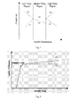
- Figure 1 represents a schematic overview of the different temperature regions for ALD growth.
- the growth rate is plot as a function of the growth temperature.
- Figure 2 represents a schematic overview of the layer thickness evolution in time for the specific conditions H1 and S1 as shown in figure 1.
- Figure 3 represents a schematic illustration of SiO 2 etched in H 2 ambient resulting in H-terminated surface.
- Figure 4 represents a schematic illustration of the surface reaction of TMAl on the H-terminated silicon surface.
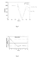
- Figure 5 represents Real-time reflectance curve of AIN growth with high or ultra-low flow TMAl predosing from the in-situ interferometer.
- Figure 6 represents the crystalline quality of as-grown AIN layers as a function of TMAl predosing time. A saturation predosing time is observed at about 180 s.
- Figure 7 represents a HR-XRD symmetry (0002) omega-scan of Sample A (with TMAl predosing) and Sample B (without TMAl predosing).
- the FWHM of Sample A is 853 arc sec while the FWHM of Sample B is 3891 arc sec.
- Figure 8 represents a RBS/Channeling spectrum of Sample A (a) and Sample B (b).
- X min from the AIN layer of Sample A and Sample B is 3.7% and 15%, respectively.
- Figure 9 represents bright-field TEM pictures for samples that have been grown with TMAl predosing (a) and without TMAl predosing (b), along the [1120] and [1010] zone-axis respectively.
- Figure 10 represents XPS C-1s spectra of Sample A (with TMAl predosing) and Sample B (without TMAl predosing) present in (a) and (b), respectively.
- (a) two peaks were observed.
- the peak at 282 eV is from Si-C bonds while the other peak at 285 eV is from C surface contamination.
- (b) only the peak at 285 eV from C surface contamination can be observed.
- the present invention is based on the surprising discovery that a SiC (silicon carbide) atomic monolayer is formed on a Si (silicon) substrate when an organometallic compound containing aluminum is provided at an ultra low flow in the reactor.
- SiC monolayer is particularly suited for growing a group III nitride layer, more particularly an AIN layer.
- said SiC monolayer can prevent Si diffusion and can also protect the Si substrate from nitridation and can introduce compressive stress in the AlN.
- the present invention provides a method for forming, in situ, a group III nitride layer on a SiC (atomic) monolayer, comprising the steps of:
- the present invention provides a method for forming, in situ, a group III nitride layer on a SiC (atomic) monolayer, comprising the steps of:
- said organometallic compound(s) is/are provided to reach a total of (at least) 0.007 ⁇ mol, preferably of (at least) 0.008 ⁇ mol, more preferably of (at least) 0.009 ⁇ mol, and even more preferably of (at least) 0,01 ⁇ mol, for a Si substrate surface of 1 cm 2 , whereby the surface is covered to form an atomic monolayer.
- said organometallic compound(s) is/are provided by a flow of less than 5 ⁇ mol/min, preferably less than 1 pmol/min, more preferably less than 0.5 pmol/min, or less than 0.2 pmol/min, even more preferably less than 0,1 pmol/min (but not null).
- said flow is comprised between 5 pmol/min and 0.005 pmol/min, more preferably between 2 pmol/min and 0.01 pmol/min, even more preferably between 0.5 pmol/min and 0.03 pmol/min, and even more preferably between 0.1 pmol/min and 0.05 ⁇ mol/min.
- said flow of less than 5 pmol/min, preferably less than 1 pmol/min, more preferably less than 0.5 pmol/min, or less than 0.2 pmol/min, even more preferably less than 0,1 pmol/min (but not null), is also referred to as ultra-low flow or ultra-low dose.
- the step (b) of providing said organometallic compounds can be referred to as the "predosing step”.
- said organometallic compound(s) decompose (s) and provide (s) methyl or ethyl groups.
- Said organometallic compound(s) can be selected from the group consisting of trimethylaluminum (TMAl), DMAl-H, and triethylaluminum (TEAl).
- Said organometallic compound(s) is/are introduced in its/their gaseous form or in a gaseous composition.
- said organometallic compound(s) can be diluted in N 2 , or in any noble gas (such as He, or Ar), and preferably in H 2 gas.
- said composition can consist of H 2 and at least one organometallic compound containing Al. More preferably, said composition consists of H 2 and one organometallic compound wherein the metal is Al.
- Said gaseous composition can further comprise traces of nitrogen (whether intentional or not), which can react with the Si substrate for forming SiN, resulting in a substrate partially covered with SiC and partially covered with SiN.
- a method of the invention can be carried out in an ALD reactor or a CBE reactor, and preferably in a MOVPE reactor.
- the precursors are introduced at the same time.
- the precursors are supplied alternatively (i.e. consecutively, or successively).
- Said group III nitride layer of step (c) can comprise or consist of AlN, GaN, AlGaN, InGaN, AlInGaN.
- said group III nitride layer of step (c) is an AIN layer.
- an epitaxial layer is formed on said SiC monolayer.
- An excellent crystalline quality can be achieved by carrying out a method according to the invention.
- AIN layers exhibiting a FWHM of about 800 arc sec. and GaN layers exhibiting a FWHM of less than 300 arc sec. could be obtained.
- FWHM refers to the full width at half maximum measured in accordance with standard methods for determining crystal quality, such as a X-ray rocking curve (0002) omega scan method.
- the temperature of the Si substrate is preferably comprised between (about) 500°C and (about) 1400°C, preferably between (about) 800°C and (about) 1400°C, more preferably between (about) 900°C and (about) 1300°C and even more preferably between (about) 1000°C and (about) 1200°C.
- the pressure in the reactor is preferably comprised between (about) le-5 mbar and (about) 1,33 bar.
- the pressure is preferably comprised between 1,33 mbar and 1,33 bar; and for CBE or ALD, the pressure is preferable comprised between 1e-5 mbar and 1.33 mbar.
- a further group III nitride layer can be deposited on the layer formed in step (c).
- Said further group III nitride layer preferably comprises or consists of a GaN layer, AlGaN layer, InGaN layer, AlInGaN layer or the like. Accordingly, a method according to the invention can further comprise, after step (c), a step (d) of forming said further group III nitride layer.
- a method for growing (forming) a SiC layer upon a SiC monolayer is also provided.
- Said method also comprises the step (a) of providing a Si substrate, the step (b) of providing at least one organometallic compound which contains Al (preferably one or more organometallic compounds wherein the metal is Al), and the step (c), wherein in step (c), suitable precursors for forming said SiC layer is provided, whereby a SiC layer continues growing (upon said SiC monolayer).
- said method for growing a SiC layer is a method according to the invention wherein, instead of providing group III nitride layer precursors, suitable SiC layer precursors are provided in step (c).
- a method according to the invention can be used for manufacturing semiconductor devices such as a Field Effect Transistor (FET) device (such as a High Electron Mobility Transistor (HEMT) device), a Light Emitting Diode (LED), a UV sensor, or a solar cell, etc.
- FET Field Effect Transistor
- HEMT High Electron Mobility Transistor
- LED Light Emitting Diode
- solar cell etc.
- SiC can be grown on silicon at high temperature ( ⁇ 1100°C) in self-limiting region (i.e. self-limiting conditions) by MOVPE.
- group-III nitrides are normally grown in mass-transport-limiting region/conditions and the growth rate of epitaxial films is determined by the flux of precursors.
- compound semiconductors are grown in MOVPE reactor, two or more precursors are introduced to the reactor at the same time.
- the organometallic compounds e.g. TMAl
- MOVPE is carried out in self-limiting region/conditions by providing ultra-low dose of said organometallic compounds (e.g. TMA1).
- said organometallic compound is trimmethylaluminum (TMA1).
- the silicon surface is carbonized (or passivated) by methyl groups decomposed from TMAl, since one SiC monolayer or less than a monolayer (e.g. when the surface is partially covered by SiN) can be observed, grown in self-limiting region/conditions. To the contrary, no accumulation of aluminum atoms on the silicon substrate is observed.
- An AIN layer is formed by providing Al precursors (e.g. TMAl) and nitrogen precursors (e.g. ammonia or hydrazine).
- Al precursors e.g. TMAl
- nitrogen precursors e.g. ammonia or hydrazine
- Wide bandgap semiconductors can then be grown.
- low temperature region low temperature region
- median temperature region high temperature region
- the reaction can be dominated by precursor decomposition, as shown by curve H2; or dominated by precursor desorption, as shown by curve H1.
- Figure 2 shows that in the self-limiting region/conditions, the as-grown thickness has a saturation level and cannot increase further by prolonging the growth time.
- This figure 2 shows also that a thicker layer can be observed in H1 case.
- the decomposition temperature of TMAl is around 260°C and the growth temperature of group-III Nitride materials is normally beyond 1000°C.
- TMAl is decomposed to methyl groups and Aluminium atoms at high temperature as follows: Al(CH 3 ) s 3 ⁇ AlCH + 2CH 4 .
- methyl groups and Al atoms are bound to the surface of silicon substrate. Meanwhile, desorption also occurs. Al atoms may diffuse into the silicon substrates or be evaporated back to the carrier gas.
- a possible explanation of the present invention is that: by providing an ultra-low flow of precursors, equilibrium between decomposition and desorption is achieved and thus no aluminum atoms are accumulated on the surface, because the bond between methyl groups and silicon atoms is stronger. Finally the silicon surface is carbonized (and consequently passivated) by the methyl groups.
- Said ultra-low TMAl dose is introduced into the reactor prior to the actual growth of AIN.
- Methyl resulting from the decomposition of the metalorganic compounds, is used to carbonize the Si substrate.
- a SiC/Si(111) template obtained by carrying out a method of the invention appears to be very suitable for further growth of AlN with very high epitaxial quality and low stress.
- the present invention also provides a device obtainable by a method according to the invention, such as a FET device, a LED, a UV sensor, or a solar cell.
- the device obtainable by a method according to the invention can be characterized by the presence, between the Si substrate and the layer formed in step (c), of a SiC (atomic) monolayer.
- Said device can be further characterized by the high quality of the crystal grown upon said SiC monolayer. More particularly, an epitaxial grown AIN layer exhibits a FWHM of less than 1000 arc sec., preferably of less than 950 arc sec., more preferably of less than 900 arc sec., even more preferably of less than 850 arc sec, and even more preferably of about 800 arc sec.
- an epitaxial grown GaN layer, grown on top of AlN exhibits a FWHM of less than 450 arc sec., preferably of less than 400 arc sec., more preferably of less than 350 arc sec., even more preferably of less than 300 arc sec.
- silicon wafers are chemically cleaned prior to loading into the Vertical 3x2" Close Coupled showerhead (CCS) MOVPE reactor.
- CCS Vertical 3x2" Close Coupled showerhead
- the substrates are annealed at 1100°C in H 2 for 10 min, resulting in a H-terminated Silicon surface ( Figure 3).
- the hydrogen-terminated surface can also be partially nitridated.
- TMA1 is introduced into the MOVPE reactor.
- the flow of TMAl is ultra-low, around 0,07 pmol/min.
- TMAl is decomposed in the H 2 ambient as: Al(CH 3 ) 3 ⁇ AlCH + 2CH 4 , and the decomposed TMAl can react with hydrogen-terminated surface (Figure 4).
- SiC is formed on the silicon surface by a reaction between a methyl group and silicon. Aluminium is considered to play the role of a catalyst by lowering the energy barrier for the carbonization reaction.
- the silicon substrates are exposed to the ultra-low flow for 180 sec., resulting in one monolayer of SiC formation on the silicon substrates.
- An in-situ real-time reflectance monitoring system is installed in the reactor (the same as in example 1).
- TMAl When TMAl is provided within a standard flow (i.e. about 25 to 30 ⁇ mol/min for the reactor used), accumulation of aluminum atoms on the silicon substrate is observed from increasing reflectance.
- the graphs of figure 6 illustrate the quality in a 180 nm thick AlN layer grown on Si versus the TMAl predosing time.
- the omega scan FWHM is between 800 arc sec and 1500 arc sec.
- the FWHM is a factor 4 higher than for the optimized predosing time.
- the figure 7 gives the HR-XRD (0002) omega-scan of samples with and without TMAl predosing.
- the FWHM of sample with TMAl predosing is as narrow as 853 arc sec while the FWHM of sample without TMA1 predosing is larger than 3600 arc sec (or higher than 1 degree).
- the graph of figure 8 shows a random and channeled spectrum for a sample with TMAl predosing.
- the minimum backscattering yield ( ⁇ min ) from the AIN layer and Si substrate respectively is 15% and 51% for samples without predosing and 3.7% and 36% for samples that have been treated with TMAl predosing.
- XPS as well as TEM measurements reveal the presence of an interface layer between the AlN and Si substrate.
- Figure 9 represents bright-field TEM pictures for a sample that has been grown with TMAl predosing (Fig. 9a) and without TMAl predosing (Fig. 9b), along the [1120] and [1010] zone-axis respectively.
- the interface layer equivalent of 2 to 3 ML, is build up out of a mixture of Si, Al, N and C, as can be deduced from a chemical profile perpendicular to the AIN/Si interface.
- XPS also reveals a reduction of the nitridation of the Si substrate prior to AlN growth, which is in agreement with the TEM results obtained for AlN layer grown of Si without predosing.
Landscapes
- Chemical & Material Sciences (AREA)
- Engineering & Computer Science (AREA)
- Materials Engineering (AREA)
- Metallurgy (AREA)
- Organic Chemistry (AREA)
- Chemical Kinetics & Catalysis (AREA)
- General Chemical & Material Sciences (AREA)
- Crystallography & Structural Chemistry (AREA)
- Mechanical Engineering (AREA)
- Inorganic Chemistry (AREA)
- Led Devices (AREA)
- Light Receiving Elements (AREA)
Abstract
The present invention relates to semiconductor process technology and devices.
In particular, the present invention relates to a method for forming a high quality group III nitride layer on a silicon substrate and to a device obtainable therefrom.
In particular, the present invention relates to a method for forming a high quality group III nitride layer on a silicon substrate and to a device obtainable therefrom.
Description
- The present invention relates to semiconductor process technology and devices.
- In particular, the present invention relates to a method for forming a high quality group III nitride layer on a silicon substrate and to a device obtainable therefrom.
- Wide bandgap semiconductors, including SiC, AlN and GaN related materials, have attracted much interest lately. In order to obtain high-quality GaN layers on Si, a growth method with different steps is used to accommodate for the large lattice and thermal mismatch between GaN and Si. AlGaN layers have been successfully used over the last years as templates for the growth of GaN on Si.
- The use of an AlN buffer layer between the silicon substrate and the GaN layer is known in the prior art.
-
US 2004/0119063 recites a device wherein a few monolayers of aluminum are deposited on the silicon substrate to protect the silicon substrate from ammonia and then forming a nucleation layer of AIN and a buffer structure including multiple superlattices of AlGaN semiconductor having different compositions and an intermediate layer of GaN or another Ga-rich nitride semiconductor. This results in an improved crystalline structure. - Chen et al (Journal of Crystal Growth 225 (2001) 150-154) describes the formation of high quality GaN on Si (111) substrate using an AlN buffer layer. Al was pre-seeded on the silicon surface to avoid formation of SixNy, which is believed to be the major impediments for nitride growth on silicon. 3 samples were prepared with various aluminum pre-seeding time of 0, 5 and 10 s. 5 s Al pre-seeding improved the surface morphology of the AlN nucleation layer much and a step-flow 2-D growth mode was clear. However, 10 s Al pre-seeding leaded to a 3-D growth mode of the AlN nucleation layer, which was claimed to be due to too much aluminum accumulated on the silicon surface.
- On the other hand, various hydrocarbons have been applied to carbonize the silicon surface, however this requires a much higher substrate temperature and results in a rough interface between SiC and Si surface prior to the formation of AlN. But this method is not convenient since it requires ex situ processing steps.
- It is an aim of the invention to provide an improved method for growing AlN on a silicon substrate.
- Further, it is an aim to provide an improved method for growing a wide bandgap material, such as group III nitride material, on silicon.
- Further, it is an aim to provide an improved method for growing SiC on a silicon substrate.
- The present invention provides a method for forming, in situ, a group III nitride layer on a SiC (atomic) monolayer, comprising the steps of:
- a) providing a Si substrate in a reactor,
- b) providing at least 0,01 µmol/cm2 of one or more organometallic compounds containing Al, in a flow of less than 5 µmol/min, preferably less than 1 µmol/min, more preferably less than 0.2 µmol/min, even more preferably less than 0,1 µmol/min (but not null), and
- c) providing the precursors suitable for forming a group III nitride layer.
- The present invention also provides a method for forming, in situ, a SiC layer on a SiC (atomic) monolayer, comprising the steps of:
- a) providing a Si substrate in a reactor,
- b) providing at least 0,01 µmol/cm2 of one or more organometallic compounds containing Al, in a flow of less than 5 µmol/min, preferably less than 1 µmol/min, more preferably less than 0.2 µmol/min, even more preferably less than 0,1 µmol/min (but not null), and
- c) providing the precursors suitable for continuing forming a SiC layer.
- Preferably, in a method according to the invention, Al (aluminum) is the metal of said organometallic compound(s) (also referred to as metalorganic compound(s)).
- Preferably, said organometallic compound(s) provide(s) methyl or ethyl groups for reacting with said Si substrate.
- Preferably, said organometallic compound(s) is/are selected from the group consisting of trimethylaluminum (TMAl), dimethlyaluminum hydride (DMAl-H), and triethylaluminum (TEAl) .
- In a method of the invention, said reactor can be a MetalOrganic Chemical Vapour Deposition (MOCVD) reactor (also referred to as a MetalOrganic Vapour Phase Epitaxy (MOVPE) reactor), an Atomic Layer Deposition (ALD) reactor or a Chemical Beam Epitaxy (CBE) reactor.
- Preferably, said group III nitride layer or said SiC layer, formed on said SiC monolayer, is an epitaxial layer.
- Preferably, said group III nitride layer is an AlN layer.
- In a method according to the invention, the temperature of the Si substrate can be comprised between (about) 500°C and (about) 1400°C, preferably between (about) 800°C and (about) 1400°C, more preferably between (about) 900°C and (about) 1300°C and even more preferably between (about) 1000°C and (about) 1200°C.
- In a method according to the invention, the pressure in the reactor is preferably comprised between (about) le-5 mbar and (about) 1,33 bar.
- For MOVPE, the pressure in the reactor is preferably comprised between 1.33 mbar and 1.33 bar.
- In case of ALD or CBE the pressure is preferably comprised between 1e-5 mbar and 1.33 mbar.
- A method according to the invention can further comprise, after step (c), a step of forming a further group III nitride layer (step (d)). Said further group III nitride layer can consist of a GaN layer, AlGaN layer, InGaN layer, AlInGaN layer or the like.
- A method according to the invention can be used for manufacturing semiconductor devices such as a Field Effect Transistor (FET) device (such as a High Electron Mobility Transistor (HEMT) device), a Light Emitting Diode (LED), a UV sensor, or a solar cell, etc.
- The present invention also provides a device obtainable by a method according to the invention.
- Figure 1 represents a schematic overview of the different temperature regions for ALD growth. The growth rate is plot as a function of the growth temperature.
- Figure 2 represents a schematic overview of the layer thickness evolution in time for the specific conditions H1 and S1 as shown in figure 1.
- Figure 3 represents a schematic illustration of SiO2 etched in H2 ambient resulting in H-terminated surface.
- Figure 4 represents a schematic illustration of the surface reaction of TMAl on the H-terminated silicon surface.
- Figure 5 represents Real-time reflectance curve of AIN growth with high or ultra-low flow TMAl predosing from the in-situ interferometer.
- Figure 6 represents the crystalline quality of as-grown AIN layers as a function of TMAl predosing time. A saturation predosing time is observed at about 180 s.
- Figure 7 represents a HR-XRD symmetry (0002) omega-scan of Sample A (with TMAl predosing) and Sample B (without TMAl predosing). The FWHM of Sample A is 853 arc sec while the FWHM of Sample B is 3891 arc sec.
- Figure 8 represents a RBS/Channeling spectrum of Sample A (a) and Sample B (b). Xmin from the AIN layer of Sample A and Sample B is 3.7% and 15%, respectively.
- Figure 9 represents bright-field TEM pictures for samples that have been grown with TMAl predosing (a) and without TMAl predosing (b), along the [1120] and [1010] zone-axis respectively.
- Figure 10 represents XPS C-1s spectra of Sample A (with TMAl predosing) and Sample B (without TMAl predosing) present in (a) and (b), respectively. In (a), two peaks were observed. The peak at 282 eV is from Si-C bonds while the other peak at 285 eV is from C surface contamination. In (b), only the peak at 285 eV from C surface contamination can be observed.
- The present invention will be described with respect to particular embodiments and with reference to certain drawings.
- The drawings described are only schematic and are non-limiting. In the drawings, the size of some of the elements may be exaggerated and not drawn on scale for illustrative purposes. The dimensions and the relative dimensions do not correspond to actual reductions to practice of the invention.
- The present invention is based on the surprising discovery that a SiC (silicon carbide) atomic monolayer is formed on a Si (silicon) substrate when an organometallic compound containing aluminum is provided at an ultra low flow in the reactor.
- It appears that the presence of said SiC monolayer is particularly suited for growing a group III nitride layer, more particularly an AIN layer.
- Moreover, said SiC monolayer can prevent Si diffusion and can also protect the Si substrate from nitridation and can introduce compressive stress in the AlN.
- The present invention provides a method for forming, in situ, a group III nitride layer on a SiC (atomic) monolayer, comprising the steps of:
- a) providing a Si substrate in a reactor,
- b) providing at least 0,01 µmol/cm2 of one or more organometallic compounds containing Al, in a flow of less than 5 µmol/min, preferably less than 1 µmol/min, more preferably less than 0.2 µmol/min, even more preferably less than 0,1 µmol/min (but not null), and
- c) providing the precursors suitable for forming a group III nitride layer.
- More particularly, the present invention provides a method for forming, in situ, a group III nitride layer on a SiC (atomic) monolayer, comprising the steps of:
- a) providing a Si substrate in a reactor,
- b) providing at least one organometallic compound wherein the metal is Al, in a flow of less than 5 pmol/min, and then
- c) providing the precursors suitable for forming a group III nitride layer upon said SiC monolayer.
- Preferably, in a method according to the invention, said organometallic compound(s) is/are provided to reach a total of (at least) 0.007 µmol, preferably of (at least) 0.008 µmol, more preferably of (at least) 0.009 µmol, and even more preferably of (at least) 0,01 µmol, for a Si substrate surface of 1 cm2, whereby the surface is covered to form an atomic monolayer.
- Moreover, said organometallic compound(s) is/are provided by a flow of less than 5 µmol/min, preferably less than 1 pmol/min, more preferably less than 0.5 pmol/min, or less than 0.2 pmol/min, even more preferably less than 0,1 pmol/min (but not null).
- Preferably, said flow is comprised between 5 pmol/min and 0.005 pmol/min, more preferably between 2 pmol/min and 0.01 pmol/min, even more preferably between 0.5 pmol/min and 0.03 pmol/min, and even more preferably between 0.1 pmol/min and 0.05 µmol/min.
- In the context of the present invention, said flow of less than 5 pmol/min, preferably less than 1 pmol/min, more preferably less than 0.5 pmol/min, or less than 0.2 pmol/min, even more preferably less than 0,1 pmol/min (but not null), is also referred to as ultra-low flow or ultra-low dose.
- In the context of the present invention, the step (b) of providing said organometallic compounds can be referred to as the "predosing step".
- Preferably, said organometallic compound(s) decompose (s) and provide (s) methyl or ethyl groups. Said organometallic compound(s) can be selected from the group consisting of trimethylaluminum (TMAl), DMAl-H, and triethylaluminum (TEAl).
- Said organometallic compound(s) is/are introduced in its/their gaseous form or in a gaseous composition.
- In particular, said organometallic compound(s) can be diluted in N2, or in any noble gas (such as He, or Ar), and preferably in H2 gas.
- In other words, said composition can consist of H2 and at least one organometallic compound containing Al. More preferably, said composition consists of H2 and one organometallic compound wherein the metal is Al.
- Said gaseous composition can further comprise traces of nitrogen (whether intentional or not), which can react with the Si substrate for forming SiN, resulting in a substrate partially covered with SiC and partially covered with SiN.
- A method of the invention can be carried out in an ALD reactor or a CBE reactor, and preferably in a MOVPE reactor.
- Usually, in a MOVPE reactor, the precursors are introduced at the same time. In the present invention, the precursors are supplied alternatively (i.e. consecutively, or successively).
- Said group III nitride layer of step (c) can comprise or consist of AlN, GaN, AlGaN, InGaN, AlInGaN.
- Preferably, said group III nitride layer of step (c) is an AIN layer.
- Preferably, an epitaxial layer is formed on said SiC monolayer.
- An excellent crystalline quality can be achieved by carrying out a method according to the invention.
- Indeed, for the first time, and for a film thickness of less than 10 µm, AIN layers exhibiting a FWHM of about 800 arc sec. and GaN layers exhibiting a FWHM of less than 300 arc sec. could be obtained.
- In the context of the present invention, FWHM refers to the full width at half maximum measured in accordance with standard methods for determining crystal quality, such as a X-ray rocking curve (0002) omega scan method.
- In a method according to the invention, the temperature of the Si substrate is preferably comprised between (about) 500°C and (about) 1400°C, preferably between (about) 800°C and (about) 1400°C, more preferably between (about) 900°C and (about) 1300°C and even more preferably between (about) 1000°C and (about) 1200°C.
- The pressure in the reactor is preferably comprised between (about) le-5 mbar and (about) 1,33 bar. In particular, for MOVPE the pressure is preferably comprised between 1,33 mbar and 1,33 bar; and for CBE or ALD, the pressure is preferable comprised between 1e-5 mbar and 1.33 mbar.
- A further group III nitride layer can be deposited on the layer formed in step (c). Said further group III nitride layer preferably comprises or consists of a GaN layer, AlGaN layer, InGaN layer, AlInGaN layer or the like. Accordingly, a method according to the invention can further comprise, after step (c), a step (d) of forming said further group III nitride layer.
- A method for growing (forming) a SiC layer upon a SiC monolayer is also provided. Said method also comprises the step (a) of providing a Si substrate, the step (b) of providing at least one organometallic compound which contains Al (preferably one or more organometallic compounds wherein the metal is Al), and the step (c), wherein in step (c), suitable precursors for forming said SiC layer is provided, whereby a SiC layer continues growing (upon said SiC monolayer).
- In other words, said method for growing a SiC layer is a method according to the invention wherein, instead of providing group III nitride layer precursors, suitable SiC layer precursors are provided in step (c).
- Except for the precursors, the same features and conditions applies.
- A method according to the invention can be used for manufacturing semiconductor devices such as a Field Effect Transistor (FET) device (such as a High Electron Mobility Transistor (HEMT) device), a Light Emitting Diode (LED), a UV sensor, or a solar cell, etc.
- In the present invention, SiC can be grown on silicon at high temperature (~1100°C) in self-limiting region (i.e. self-limiting conditions) by MOVPE.
- In MOVPE, group-III nitrides are normally grown in mass-transport-limiting region/conditions and the growth rate of epitaxial films is determined by the flux of precursors. When compound semiconductors are grown in MOVPE reactor, two or more precursors are introduced to the reactor at the same time.
- In a method according to the present invention, the organometallic compounds (e.g. TMAl) are first introduced in the reactor. MOVPE is carried out in self-limiting region/conditions by providing ultra-low dose of said organometallic compounds (e.g. TMA1).
- According to a preferred embodiment, said organometallic compound is trimmethylaluminum (TMA1).
- The silicon surface is carbonized (or passivated) by methyl groups decomposed from TMAl, since one SiC monolayer or less than a monolayer (e.g. when the surface is partially covered by SiN) can be observed, grown in self-limiting region/conditions. To the contrary, no accumulation of aluminum atoms on the silicon substrate is observed.
- An AIN layer is formed by providing Al precursors (e.g. TMAl) and nitrogen precursors (e.g. ammonia or hydrazine).
- Wide bandgap semiconductors can then be grown.
- It is to be noted that self-limiting growth was first used in ALD method.
- Referring to figure 1, three temperature regions are represented: low temperature region, median temperature region and high temperature region.
- In the low temperature region the heterogeneous reaction rate is too slow (L1), or in case of multi-layer adsorption (L2), self-limiting conditions are not reached.
- In the high temperature region, the reaction can be dominated by precursor decomposition, as shown by curve H2; or dominated by precursor desorption, as shown by curve H1.
- In the median temperature region, self-limiting reaction/conditions (S1, S2) is/are achieved.
- Figure 2 shows that in the self-limiting region/conditions, the as-grown thickness has a saturation level and cannot increase further by prolonging the growth time.
- This figure 2 shows also that a thicker layer can be observed in H1 case.
- The decomposition temperature of TMAl is around 260°C and the growth temperature of group-III Nitride materials is normally beyond 1000°C.
- From the classical point of view, group-III nitrides are not grown in self-limiting region/conditions. And at high temperature, both precursor decomposition rate and desorption rate are enhanced. TMAl is decomposed to methyl groups and Aluminium atoms at high temperature as follows:
Al(CH3)s 3 ↔ AlCH + 2CH4.
- Then, methyl groups and Al atoms are bound to the surface of silicon substrate. Meanwhile, desorption also occurs. Al atoms may diffuse into the silicon substrates or be evaporated back to the carrier gas.
- A possible explanation of the present invention, is that: by providing an ultra-low flow of precursors, equilibrium between decomposition and desorption is achieved and thus no aluminum atoms are accumulated on the surface, because the bond between methyl groups and silicon atoms is stronger. Finally the silicon surface is carbonized (and consequently passivated) by the methyl groups.
- Said ultra-low TMAl dose is introduced into the reactor prior to the actual growth of AIN.
- Methyl, resulting from the decomposition of the metalorganic compounds, is used to carbonize the Si substrate.
- A SiC/Si(111) template obtained by carrying out a method of the invention, appears to be very suitable for further growth of AlN with very high epitaxial quality and low stress.
- The present invention also provides a device obtainable by a method according to the invention, such as a FET device, a LED, a UV sensor, or a solar cell.
- The device obtainable by a method according to the invention can be characterized by the presence, between the Si substrate and the layer formed in step (c), of a SiC (atomic) monolayer.
- Said device can be further characterized by the high quality of the crystal grown upon said SiC monolayer. More particularly, an epitaxial grown AIN layer exhibits a FWHM of less than 1000 arc sec., preferably of less than 950 arc sec., more preferably of less than 900 arc sec., even more preferably of less than 850 arc sec, and even more preferably of about 800 arc sec.
- Similarly, an epitaxial grown GaN layer, grown on top of AlN, exhibits a FWHM of less than 450 arc sec., preferably of less than 400 arc sec., more preferably of less than 350 arc sec., even more preferably of less than 300 arc sec.
- The invention is described in further details in the following examples, which are intended for illustration purposes only, and should not be construed as limiting the scope of the invention in any way.
- In a first step, silicon wafers are chemically cleaned prior to loading into the Vertical 3x2" Close Coupled Showerhead (CCS) MOVPE reactor. The substrates are annealed at 1100°C in H2 for 10 min, resulting in a H-terminated Silicon surface (Figure 3).
- Due to the decomposition of GaN and AlGaN alloy deposited (during prior uses) on the susceptor and the liner, the hydrogen-terminated surface can also be partially nitridated.
- Then TMA1 is introduced into the MOVPE reactor. The flow of TMAl is ultra-low, around 0,07 pmol/min. At 1100°C, TMAl is decomposed in the H2 ambient as: Al(CH3)3 ↔ AlCH + 2CH4, and the decomposed TMAl can react with hydrogen-terminated surface (Figure 4).
- SiC is formed on the silicon surface by a reaction between a methyl group and silicon. Aluminium is considered to play the role of a catalyst by lowering the energy barrier for the carbonization reaction.
- The silicon substrates are exposed to the ultra-low flow for 180 sec., resulting in one monolayer of SiC formation on the silicon substrates.
- Then, the flow of TMAl is raised to a standard of 27,3 pmol/min and NH3 is provided in a flow of 100 sccm, resulting in a -180 nm AIN layer, grown on SiC/Si (111) templates.
- Good quality of AIN with low growth stress is achieved.
- An in-situ real-time reflectance monitoring system is installed in the reactor (the same as in example 1).
- When TMAl is provided within a standard flow (i.e. about 25 to 30 µmol/min for the reactor used), accumulation of aluminum atoms on the silicon substrate is observed from increasing reflectance.
- On the other hand, when working in self-limiting region/conditions, no change in reflectance can be seen.
- The graphs of figure 6 illustrate the quality in a 180 nm thick AlN layer grown on Si versus the TMAl predosing time.
- For 180nm AlN, the omega scan FWHM is between 800 arc sec and 1500 arc sec.
- A minimum in both FWHM can be found for a predosing time of 180 sec.
- For a predosing time of 0 sec, (i.e. no predosing), the FWHM is a factor 4 higher than for the optimized predosing time.
- The figure 7 gives the HR-XRD (0002) omega-scan of samples with and without TMAl predosing.
- The FWHM of sample with TMAl predosing is as narrow as 853 arc sec while the FWHM of sample without TMA1 predosing is larger than 3600 arc sec (or higher than 1 degree).
- RBS/Channeling measurements on both samples grown with and without predosing also reveal an improvement in crystalline quality for the first type of samples.
- The graph of figure 8 shows a random and channeled spectrum for a sample with TMAl predosing.
- The minimum backscattering yield (χmin) from the AIN layer and Si substrate respectively is 15% and 51% for samples without predosing and 3.7% and 36% for samples that have been treated with TMAl predosing.
- A drastic reduction in χmin for both the Al and Si signal is observed. The reduction in the Al signal is a result of the improved crystalline quality of the AlN layer, while the reduction of the Si signal suggests a smaller dechanneling effect caused by structural defects at the interface between the substrate and the AlN film.
- XPS as well as TEM measurements reveal the presence of an interface layer between the AlN and Si substrate.
- Figure 9 represents bright-field TEM pictures for a sample that has been grown with TMAl predosing (Fig. 9a) and without TMAl predosing (Fig. 9b), along the [1120] and [1010] zone-axis respectively.
- When the substrate is treated with TMAl predosing, the interface layer, equivalent of 2 to 3 ML, is build up out of a mixture of Si, Al, N and C, as can be deduced from a chemical profile perpendicular to the AIN/Si interface.
- In XPS measurements, the presence of the C-1s peak from SiC could be clearly identified, next to the C-1s peak coming from the C surface contamination.
- This peak is not present for samples which have not been grown using the predosing method, as can be seen on the graphs of figure 10 (Fig. 10a: with predosing, Fig. 10b: without predosing).
- XPS also reveals a reduction of the nitridation of the Si substrate prior to AlN growth, which is in agreement with the TEM results obtained for AlN layer grown of Si without predosing.
Claims (14)
- A method for forming, in situ, a group III nitride layer or a SiC layer on a SiC (atomic) monolayer, comprising the steps of:a) providing a Si substrate in a reactor,b) providing at least 0,01 µmol/cm2 of one or more organometallic compounds containing Al, in a flow of less than 5 µmol/min, andc) providing the precursors suitable for forming a group III nitride layer, or providing the precursors suitable for continuing the growth of a SiC layer.
- A method according to claim 1, wherein said flow is less than 0,1 µmol/min.
- A method according to claim 1 or 2, wherein the metal in said organometallic compound(s) is Al.
- A method according to any of claims 1 to 3, wherein said organometallic compound(s) provide(s) methyl or ethyl groups for reacting with the Si substrate.
- A method according to any of claims 1 to 4, wherein said organometallic compound(s) is/are selected from the group consisting of trimethylaluminum (TMAl), dimethlyaluminum hydride (DMAI-H), and triethylaluminum (TEAl) .
- A method according to any of claims 1 to 5, wherein said reactor is a metalorganic chemical vapour deposition reactor, an atomic layer deposition reactor or a chemical beam epitaxy reactor.
- A method according to any of claims 1 to 6, wherein said group III nitride layer or said SiC layer, formed on said SiC monolayer, is an epitaxial layer.
- A method according to any of claims 1 to 7, wherein said group III nitride layer is an AlN layer.
- A method according to any of claims 1 to 8, wherein the temperature of the Si substrate is comprised between about 500°C and about 1400°C.
- A method according to any of claims 1 to 9, wherein the pressure in the reactor is comprised between about 1e-5 mbar and about 1,33 bar.
- A method according to any of claims 1 to 10, further comprising, after step (c), a step (d) of forming a further group III nitride layer.
- A method according to claim 11, wherein said further group III nitride layer consists of a GaN layer, AlGaN layer, InGaN layer, or AlInGaN layer.
- Use of a method according to any of claims 1 to 12 for manufacturing a FET device (such as a HEMT device), a LED, a UV sensor, or a solar cell.
- A device obtainable by a method according to any of claims 1 to 13.
Priority Applications (4)
| Application Number | Priority Date | Filing Date | Title |
|---|---|---|---|
| US11/690,509 US7666765B2 (en) | 2006-04-06 | 2007-03-23 | Method for forming a group III nitride material on a silicon substrate |
| EP07104838.3A EP1842941B1 (en) | 2006-04-06 | 2007-03-23 | Method for forming a group iii nitride material or a sic material on a silicon substrate |
| JP2007099049A JP5334377B2 (en) | 2006-04-06 | 2007-04-05 | Method for laminating a group III nitride material on a silicon substrate |
| US12/502,940 US7989925B2 (en) | 2006-04-06 | 2009-07-14 | Method for forming a group III nitride material on a silicon substrate |
Applications Claiming Priority (1)
| Application Number | Priority Date | Filing Date | Title |
|---|---|---|---|
| US78986106P | 2006-04-06 | 2006-04-06 |
Publications (1)
| Publication Number | Publication Date |
|---|---|
| EP1842940A1 true EP1842940A1 (en) | 2007-10-10 |
Family
ID=37309330
Family Applications (2)
| Application Number | Title | Priority Date | Filing Date |
|---|---|---|---|
| EP06118018A Withdrawn EP1842940A1 (en) | 2006-04-06 | 2006-07-27 | Method for forming a group III nitride material on a silicon substrate |
| EP07104838.3A Active EP1842941B1 (en) | 2006-04-06 | 2007-03-23 | Method for forming a group iii nitride material or a sic material on a silicon substrate |
Family Applications After (1)
| Application Number | Title | Priority Date | Filing Date |
|---|---|---|---|
| EP07104838.3A Active EP1842941B1 (en) | 2006-04-06 | 2007-03-23 | Method for forming a group iii nitride material or a sic material on a silicon substrate |
Country Status (3)
| Country | Link |
|---|---|
| US (2) | US7666765B2 (en) |
| EP (2) | EP1842940A1 (en) |
| JP (1) | JP5334377B2 (en) |
Cited By (2)
| Publication number | Priority date | Publication date | Assignee | Title |
|---|---|---|---|---|
| EP2455964A4 (en) * | 2009-07-17 | 2014-09-03 | Dowa Electronics Materials Co Ltd | EPITAXIAL SUBSTRATE FOR ELECTRONIC DEVICE USING CROSS-STEERING DIRECTION AS DIRECTION OF CURRENT CONDUCTION, AND METHOD OF MANUFACTURING THE SAME |
| WO2024141309A1 (en) | 2022-12-28 | 2024-07-04 | Aixtron Se | Method for depositing gallium nitride gan on silicon si |
Families Citing this family (20)
| Publication number | Priority date | Publication date | Assignee | Title |
|---|---|---|---|---|
| EP1842940A1 (en) * | 2006-04-06 | 2007-10-10 | Interuniversitair Microelektronica Centrum ( Imec) | Method for forming a group III nitride material on a silicon substrate |
| US8993460B2 (en) * | 2013-01-10 | 2015-03-31 | Novellus Systems, Inc. | Apparatuses and methods for depositing SiC/SiCN films via cross-metathesis reactions with organometallic co-reactants |
| US8338210B2 (en) * | 2010-06-14 | 2012-12-25 | Asm International N.V. | Method for processing solar cell substrates |
| JP5668339B2 (en) * | 2010-06-30 | 2015-02-12 | 住友電気工業株式会社 | Manufacturing method of semiconductor device |
| JP5614130B2 (en) * | 2010-06-30 | 2014-10-29 | 住友電気工業株式会社 | Manufacturing method of semiconductor device |
| US8541769B2 (en) | 2010-11-09 | 2013-09-24 | International Business Machines Corporation | Formation of a graphene layer on a large substrate |
| US20120112198A1 (en) * | 2010-11-09 | 2012-05-10 | International Business Machines Corporation | Epitaxial growth of silicon carbide on sapphire |
| WO2013063038A1 (en) * | 2011-10-24 | 2013-05-02 | Rosestreet Labs, Llc | Nitride uv light sensors on silicon substrates |
| US8937298B2 (en) | 2011-10-24 | 2015-01-20 | Rosestreet Labs, Llc | Structure and method for forming integral nitride light sensors on silicon substrates |
| US8946775B2 (en) | 2012-08-22 | 2015-02-03 | Industrial Technology Research Institute | Nitride semiconductor structure |
| US9685513B2 (en) | 2012-10-24 | 2017-06-20 | The United States Of America, As Represented By The Secretary Of The Navy | Semiconductor structure or device integrated with diamond |
| US8981382B2 (en) | 2013-03-06 | 2015-03-17 | Iqe Rf, Llc | Semiconductor structure including buffer with strain compensation layers |
| WO2014152598A1 (en) | 2013-03-15 | 2014-09-25 | The Government Of The United States Of America, As Represented By The Secretary Of The Navy | Nanocrystalline diamond three-dimensional films in patterned semiconductor substrates |
| KR102083823B1 (en) * | 2013-12-24 | 2020-04-14 | 에스케이하이닉스 주식회사 | Display driving device removing offset voltage |
| US9917156B1 (en) | 2016-09-02 | 2018-03-13 | IQE, plc | Nucleation layer for growth of III-nitride structures |
| JP6903857B2 (en) * | 2017-06-02 | 2021-07-14 | 住友電工デバイス・イノベーション株式会社 | Semiconductor substrate manufacturing method |
| EP3503163A1 (en) * | 2017-12-21 | 2019-06-26 | EpiGan NV | A method for forming a silicon carbide film onto a silicon substrate |
| CN112750904B (en) | 2019-10-30 | 2024-01-02 | 联华电子股份有限公司 | Semiconductor component with stress relaxation layer |
| US20240266169A1 (en) | 2021-06-11 | 2024-08-08 | Jusung Engineering Co., Ltd. | Power semiconductor device manufacturing method |
| US11784189B2 (en) | 2021-08-20 | 2023-10-10 | Globalfoundries U.S. Inc. | Monolithic integration of diverse device types with shared electrical isolation |
Citations (4)
| Publication number | Priority date | Publication date | Assignee | Title |
|---|---|---|---|---|
| EP0322615A1 (en) * | 1987-12-19 | 1989-07-05 | Fujitsu Limited | Method of growing a single crystalline beta-silicon carbide layer on a silicon substrate |
| US5471946A (en) * | 1992-10-13 | 1995-12-05 | Cs Halbleiter-Und Solartechnologie Gmbh | Method for producing a wafer with a monocrystalline silicon carbide layer |
| US20040029365A1 (en) * | 2001-05-07 | 2004-02-12 | Linthicum Kevin J. | Methods of fabricating gallium nitride microelectronic layers on silicon layers and gallium nitride microelectronic structures formed thereby |
| US20040119063A1 (en) * | 2002-12-04 | 2004-06-24 | Emcore Corporation | Gallium nitride-based devices and manufacturing process |
Family Cites Families (16)
| Publication number | Priority date | Publication date | Assignee | Title |
|---|---|---|---|---|
| JP2546696B2 (en) * | 1987-12-17 | 1996-10-23 | 富士通株式会社 | Silicon carbide layer structure |
| JPH0831419B2 (en) * | 1990-12-25 | 1996-03-27 | 名古屋大学長 | Method for producing compound semiconductor single crystal on single crystal silicon substrate |
| US5861346A (en) * | 1995-07-27 | 1999-01-19 | Regents Of The University Of California | Process for forming silicon carbide films and microcomponents |
| JP2927768B1 (en) * | 1998-03-26 | 1999-07-28 | 技術研究組合オングストロームテクノロジ研究機構 | Semiconductor device and manufacturing method thereof |
| US6328796B1 (en) * | 1999-02-01 | 2001-12-11 | The United States Of America As Represented By The Secretary Of The Navy | Single-crystal material on non-single-crystalline substrate |
| JP2000277441A (en) * | 1999-03-26 | 2000-10-06 | Nagoya Kogyo Univ | Semiconductor structure, semiconductor device having the same, and crystal growth method |
| US6391748B1 (en) * | 2000-10-03 | 2002-05-21 | Texas Tech University | Method of epitaxial growth of high quality nitride layers on silicon substrates |
| US6580125B2 (en) * | 2000-11-21 | 2003-06-17 | Matsushita Electric Industrial Co., Ltd. | Semiconductor device and method for fabricating the same |
| US6811814B2 (en) | 2001-01-16 | 2004-11-02 | Applied Materials, Inc. | Method for growing thin films by catalytic enhancement |
| US6488771B1 (en) * | 2001-09-25 | 2002-12-03 | The United States Of America As Represented By The Administrator Of The National Aeronautics And Space Administration | Method for growing low-defect single crystal heteroepitaxial films |
| US6818061B2 (en) * | 2003-04-10 | 2004-11-16 | Honeywell International, Inc. | Method for growing single crystal GaN on silicon |
| KR100627888B1 (en) * | 2004-05-25 | 2006-09-25 | 도시바세라믹스가부시키가이샤 | A substrate for growth of chemical compound semiconductor, a chemical compound semiconductor using the substrate and a process for producing them |
| US8754449B2 (en) * | 2004-06-11 | 2014-06-17 | Ammono Sp. Z O.O. | High electron mobility transistor (HEMT) made of layers of Group XIII element nitrides and manufacturing method thereof |
| US7491626B2 (en) * | 2005-06-20 | 2009-02-17 | Sensor Electronic Technology, Inc. | Layer growth using metal film and/or islands |
| EP1842940A1 (en) * | 2006-04-06 | 2007-10-10 | Interuniversitair Microelektronica Centrum ( Imec) | Method for forming a group III nitride material on a silicon substrate |
| US20080251812A1 (en) * | 2007-04-16 | 2008-10-16 | Woo Sik Yoo | Heteroepitaxial Crystal Quality Improvement |
-
2006
- 2006-07-27 EP EP06118018A patent/EP1842940A1/en not_active Withdrawn
-
2007
- 2007-03-23 EP EP07104838.3A patent/EP1842941B1/en active Active
- 2007-03-23 US US11/690,509 patent/US7666765B2/en active Active
- 2007-04-05 JP JP2007099049A patent/JP5334377B2/en active Active
-
2009
- 2009-07-14 US US12/502,940 patent/US7989925B2/en active Active
Patent Citations (4)
| Publication number | Priority date | Publication date | Assignee | Title |
|---|---|---|---|---|
| EP0322615A1 (en) * | 1987-12-19 | 1989-07-05 | Fujitsu Limited | Method of growing a single crystalline beta-silicon carbide layer on a silicon substrate |
| US5471946A (en) * | 1992-10-13 | 1995-12-05 | Cs Halbleiter-Und Solartechnologie Gmbh | Method for producing a wafer with a monocrystalline silicon carbide layer |
| US20040029365A1 (en) * | 2001-05-07 | 2004-02-12 | Linthicum Kevin J. | Methods of fabricating gallium nitride microelectronic layers on silicon layers and gallium nitride microelectronic structures formed thereby |
| US20040119063A1 (en) * | 2002-12-04 | 2004-06-24 | Emcore Corporation | Gallium nitride-based devices and manufacturing process |
Cited By (3)
| Publication number | Priority date | Publication date | Assignee | Title |
|---|---|---|---|---|
| EP2455964A4 (en) * | 2009-07-17 | 2014-09-03 | Dowa Electronics Materials Co Ltd | EPITAXIAL SUBSTRATE FOR ELECTRONIC DEVICE USING CROSS-STEERING DIRECTION AS DIRECTION OF CURRENT CONDUCTION, AND METHOD OF MANUFACTURING THE SAME |
| WO2024141309A1 (en) | 2022-12-28 | 2024-07-04 | Aixtron Se | Method for depositing gallium nitride gan on silicon si |
| DE102022134874A1 (en) * | 2022-12-28 | 2024-07-04 | Aixtron Se | Process for depositing GaN on Si |
Also Published As
| Publication number | Publication date |
|---|---|
| US20090294777A1 (en) | 2009-12-03 |
| JP5334377B2 (en) | 2013-11-06 |
| JP2007281478A (en) | 2007-10-25 |
| EP1842941A1 (en) | 2007-10-10 |
| US7666765B2 (en) | 2010-02-23 |
| US20070238315A1 (en) | 2007-10-11 |
| EP1842941B1 (en) | 2018-11-07 |
| US7989925B2 (en) | 2011-08-02 |
Similar Documents
| Publication | Publication Date | Title |
|---|---|---|
| EP1842941B1 (en) | Method for forming a group iii nitride material or a sic material on a silicon substrate | |
| EP1885918B1 (en) | Methods of preparing controlled polarity group iii-nitride films | |
| US10494738B2 (en) | Growth of crystalline materials on two-dimensional inert materials | |
| KR101556054B1 (en) | SEMICONDUCTOR WAFER WITH A LAYER OF AlzGa1-zN AND PROCESS FOR PRODUCING IT | |
| Kuech et al. | Selective epitaxy in the conventional metalorganic vapor phase epitaxy of GaAs | |
| Marchand et al. | Structural and optical properties of GaN laterally overgrown on Si (111) by metalorganic chemical vapor deposition using an AlN buffer layer | |
| EP2290136A1 (en) | Method for achieving improved epitaxy quality (surface texture and defect densitity) on free-standing (aluminum, indium, gallium) nitride ((Al, In, Ga)N) substrates for opto-electronic and electronic devices | |
| US20240047203A1 (en) | Monolithic remote epitaxy of compound semi conductors and 2d materials | |
| EP1436448A1 (en) | Low temperature epitaxial growth of quaternary wide bandgap semiconductors | |
| Dupuis et al. | Selective-area and lateral epitaxial overgrowth of III-N materials by metalorganic chemical vapor deposition | |
| WO2012069520A1 (en) | Methods of forming bulk iii-nitride materials on metal-nitride growth template layers, and structures formed by such methods | |
| US9396936B2 (en) | Method for growing aluminum indium nitride films on silicon substrate | |
| US20200332438A1 (en) | A method for forming silicon carbide onto a silicon substrate | |
| Park et al. | Metal–organic chemical vapor deposition growth of GaN thin film on 3C-SiC/Si (111) substrate using various buffer layers | |
| US20090309189A1 (en) | Method for the growth of indium nitride | |
| CN101736398A (en) | Method for growing AlInN monocrystal epitaxial film | |
| Gastellóu et al. | Optical and Structural Analysis of GaN Microneedle Crystals Obtained via GaAs Substrates Decomposition and their Possible Growth Model Using the Volmer–Weber Mechanism | |
| JP7120598B2 (en) | Aluminum nitride single crystal film and method for manufacturing semiconductor device | |
| US6844574B1 (en) | III-V compound semiconductor | |
| Avramescu et al. | Growth of AlN–SiC solid solutions by sequential supply epitaxy | |
| van der Wel et al. | Area-Selective Low-Pressure Thermal Atomic Layer Deposition of Gallium Nitride | |
| WO2018080300A1 (en) | Method for producing a non-polar a-plane gallium nitride (gan) thin film on an r-plane sapphire substrate | |
| Böttcher et al. | The role of the growth temperature for the SiN interlayer deposition in GaN | |
| Mita et al. | Polarity control of GaN films grown by metal organic chemical vapor deposition on (0001) sapphire substrates | |
| Yu et al. | Characterization of AlXGa1-xN Grown by MOCVD at Low Temperatures |
Legal Events
| Date | Code | Title | Description |
|---|---|---|---|
| PUAI | Public reference made under article 153(3) epc to a published international application that has entered the european phase |
Free format text: ORIGINAL CODE: 0009012 |
|
| AK | Designated contracting states |
Kind code of ref document: A1 Designated state(s): AT BE BG CH CY CZ DE DK EE ES FI FR GB GR HU IE IS IT LI LT LU LV MC NL PL PT RO SE SI SK TR |
|
| AX | Request for extension of the european patent |
Extension state: AL BA HR MK YU |
|
| AKX | Designation fees paid | ||
| REG | Reference to a national code |
Ref country code: DE Ref legal event code: 8566 |
|
| STAA | Information on the status of an ep patent application or granted ep patent |
Free format text: STATUS: THE APPLICATION IS DEEMED TO BE WITHDRAWN |
|
| 18D | Application deemed to be withdrawn |
Effective date: 20080411 |