EP1841021A2 - Electrical connector - Google Patents
Electrical connector Download PDFInfo
- Publication number
- EP1841021A2 EP1841021A2 EP07005926A EP07005926A EP1841021A2 EP 1841021 A2 EP1841021 A2 EP 1841021A2 EP 07005926 A EP07005926 A EP 07005926A EP 07005926 A EP07005926 A EP 07005926A EP 1841021 A2 EP1841021 A2 EP 1841021A2
- Authority
- EP
- European Patent Office
- Prior art keywords
- terminal
- contact portion
- electrical connector
- housing
- contact
- Prior art date
- Legal status (The legal status is an assumption and is not a legal conclusion. Google has not performed a legal analysis and makes no representation as to the accuracy of the status listed.)
- Granted
Links
Images




Classifications
-
- H—ELECTRICITY
- H01—ELECTRIC ELEMENTS
- H01R—ELECTRICALLY-CONDUCTIVE CONNECTIONS; STRUCTURAL ASSOCIATIONS OF A PLURALITY OF MUTUALLY-INSULATED ELECTRICAL CONNECTING ELEMENTS; COUPLING DEVICES; CURRENT COLLECTORS
- H01R43/00—Apparatus or processes specially adapted for manufacturing, assembling, maintaining, or repairing of line connectors or current collectors or for joining electric conductors
- H01R43/20—Apparatus or processes specially adapted for manufacturing, assembling, maintaining, or repairing of line connectors or current collectors or for joining electric conductors for assembling or disassembling contact members with insulating base, case or sleeve
- H01R43/24—Assembling by moulding on contact members
-
- H—ELECTRICITY
- H01—ELECTRIC ELEMENTS
- H01R—ELECTRICALLY-CONDUCTIVE CONNECTIONS; STRUCTURAL ASSOCIATIONS OF A PLURALITY OF MUTUALLY-INSULATED ELECTRICAL CONNECTING ELEMENTS; COUPLING DEVICES; CURRENT COLLECTORS
- H01R12/00—Structural associations of a plurality of mutually-insulated electrical connecting elements, specially adapted for printed circuits, e.g. printed circuit boards [PCB], flat or ribbon cables, or like generally planar structures, e.g. terminal strips, terminal blocks; Coupling devices specially adapted for printed circuits, flat or ribbon cables, or like generally planar structures; Terminals specially adapted for contact with, or insertion into, printed circuits, flat or ribbon cables, or like generally planar structures
- H01R12/70—Coupling devices
- H01R12/71—Coupling devices for rigid printing circuits or like structures
- H01R12/712—Coupling devices for rigid printing circuits or like structures co-operating with the surface of the printed circuit or with a coupling device exclusively provided on the surface of the printed circuit
- H01R12/716—Coupling device provided on the PCB
-
- H—ELECTRICITY
- H01—ELECTRIC ELEMENTS
- H01R—ELECTRICALLY-CONDUCTIVE CONNECTIONS; STRUCTURAL ASSOCIATIONS OF A PLURALITY OF MUTUALLY-INSULATED ELECTRICAL CONNECTING ELEMENTS; COUPLING DEVICES; CURRENT COLLECTORS
- H01R12/00—Structural associations of a plurality of mutually-insulated electrical connecting elements, specially adapted for printed circuits, e.g. printed circuit boards [PCB], flat or ribbon cables, or like generally planar structures, e.g. terminal strips, terminal blocks; Coupling devices specially adapted for printed circuits, flat or ribbon cables, or like generally planar structures; Terminals specially adapted for contact with, or insertion into, printed circuits, flat or ribbon cables, or like generally planar structures
- H01R12/70—Coupling devices
- H01R12/71—Coupling devices for rigid printing circuits or like structures
- H01R12/72—Coupling devices for rigid printing circuits or like structures coupling with the edge of the rigid printed circuits or like structures
- H01R12/73—Coupling devices for rigid printing circuits or like structures coupling with the edge of the rigid printed circuits or like structures connecting to other rigid printed circuits or like structures
-
- H—ELECTRICITY
- H01—ELECTRIC ELEMENTS
- H01R—ELECTRICALLY-CONDUCTIVE CONNECTIONS; STRUCTURAL ASSOCIATIONS OF A PLURALITY OF MUTUALLY-INSULATED ELECTRICAL CONNECTING ELEMENTS; COUPLING DEVICES; CURRENT COLLECTORS
- H01R13/00—Details of coupling devices of the kinds covered by groups H01R12/70 or H01R24/00 - H01R33/00
- H01R13/02—Contact members
- H01R13/26—Pin or blade contacts for sliding co-operation on one side only
Definitions
- the present invention relates to electrical connectors and, particularly, to an electrical connector that the terminal is molded together with the housing.
- a connector 50 includes a housing 51 and terminals 52 that are molded together with the housing 51 as a unit.
- the terminal 52 is made by bending a metal strip in its thicknesswise direction to provide a connection section 53 and a contact section 54 indented from a peripheral portion 55 that is level with the surface of the housing 51.
- a mating connector 60 includes a housing 61 and terminals 62 that are press fitted into the housing 61. These terminals S2 are made by stamping a metal sheet to provide a press-fin section 64, a connection section 65 extending to the right from a base section 63, and a flexible arm 66 extending to the left and then upward.
- the flexible arm 66 has a curved free end to form a contact portion 67.
- the terminal 62 is held by press fitting the press-fit section. 64 into a retention slot 61A of the housing 61.
- the contact portion 67 of the mating connector 60 enters in the contact portion 54, which is intended from the peripheral portion 55, to provide stable contact.
- the connector 50 is made such that the peripheral portion 55 of the terminal 52 does not come to so close contact with the mold that the molten resin enters and sticks to the contact section 54.
- the contact portion 54 of the above connector is made by pressing a die onto a metal sheet. It is desirable that the width of the contact portion 54 is large so that the width of a peripheral edge 55 becomes very small.
- the die If the die is displaced to either side from the regular position, no side edge is formed on the side, resulting in a large gap between the metal mold and the terminal. Consequently, molten resin enters and adheres to the contact portion 54, leading to poor contact with the terminal of a mating connector.
- the lateral displacement limits the width of the contact area with the terminal of a mating connector. Consequently, the terminal of a mating connector can ride on the side edge of the contact portion, resulting in an unstable contact.
- an object of the invention to provide an electrical connector capable of preventing molten resin from entering the contact portion even if the die is displaced in its widthwise or thicknesswise direction and providing a stable contact with the terminal of a mating connector.
- a connector 1 includes a housing 2 made of an insulative material and terminals 3 molded together with the housing 1 as a unit.
- the housing 2 has a peripheral wall 6 consisting of a pair of opposed longitudinal walls 4 and a pair of opposed end walls 5.
- the peripheral wall 6 and a bottom wall 7 form a cavity 2A for receiving a mating connector.
- the terminal 3 is made by bending a metal strip in its thisknesswise direction to provide an engaging section 8 with a contact portion 8A for contact with a terminal of the mating connector and a connection section 9 projecting from the housing 1 for connection to a circuit board (not shown).
- the terminal 3 which has such a shape as shown in Fig. 3, is molded with and supported by the housing 2.
- the terminal 3 is made by bending a metal strip in its thicknesswise direction to provide a substantially L-shaped form that has the vertical flat section 8 and the horizontal connection section 9.
- the end portion of the vertical section 8 is curved to provide a curved portion 10 which increases the retaining power of the housing 2. This curved portion 10 also assures smooth introduction of the terminal of a mating connector.
- the engaging section 8 is level with the inside surface of the side wall 4 and is provided with an indented contact portion 8A.
- the contact portion 8A is made of a curved surface that is a portion of cylinder having a radius R.
- the diameter 2R is greater than the width B of the contact portion 8A so that the contact portion 8A has the slope of a tangent 11A to the side edge 11 of the terminal 3.
- the tangent 12A to the center 12 of the width becomes parallel to the plane of the terminal 3.
- the tangents 11A at both side edges 11 and the tangent 12A at the center 12 share a common circle.
- the contact portion 8A may be made of other surfaces such as three flat surfaces; two tangents to the side edges 11 and one tangent to the center 12. These flat surfaces may be connected with curved surfaces. The three tangents may contact different circles.
- the contact portion 8A which is made of a portion of cylinder, has sloped upper and lower end faces 8B and 8C in the vertical or longitudinal direction.
- the depth of the contact portion 8A becomes the maximum at the center and smaller toward the side edges so that the distance h becomes the maximum at the center and smaller toward the side edges. Consequently, the contact portion of a mating connector starts to contact the side edges at the upper end face 8B and moves to the contact portion 8A for completing the contact.
- the terminal of a mating connector is displaced in the widthwise direction, it is gradually moved toward the center for correction.
- the contact portion 8A has no sloped transitional portions or end faces but stepped ones.
- the contact portion 8A becomes deeper toward the center so that after the mating terminal reaches the contact portion 8A, it is guided in the widthwise direction.
- the operator obtains a click sense to know that the terminal reaches the contact portion 8A.
- Both the connectors are locked at the stepped portions.
- the curved surface of the contact portion 8A makes a point contact with the mating terminal, increasing the contact pressure to provide a reliable connection.
- the mating connector 20 includes a housing 21 having a peripheral wall 22 and a central wall 23 within a cavity defined by the peripheral wall 22 to provide a plugging cavity 24 for receiving the peripheral wall 6 of the connector 1.
- a plurality of terminals 25 are supported by the peripheral wall 22 and provided with contact portions 25A arranged in the plugging cavity 24.
- the terminal 24 is made by stamping a metal sheet to provide a base section 25B and a flexible arm 25C extending from the base section 25B and having the contact portion or projection 25A at its free end that is exposed in the plugging cavity 24.
- a fixing section 25D extends downward from the base section 25B and press fitted into a fixing slit 21A provided in the housing 21 so that the housing 21 supports the terminal 25.
- connection section 25E extends laterally from the base section 25B and is to be soldered to a circuit board P2.
- the mating connector 20 is not the subject matter of the application and its detailed description is omitted. That is, the mating connector may take a variety of structures.
Landscapes
- Engineering & Computer Science (AREA)
- Manufacturing & Machinery (AREA)
- Coupling Device And Connection With Printed Circuit (AREA)
- Connector Housings Or Holding Contact Members (AREA)
Abstract
Description
- The present invention relates to electrical connectors and, particularly, to an electrical connector that the terminal is molded together with the housing.
- An example of the electrical connector of this type is disclosed in
JP 2001-143801 - As shown in Fig. 7, a
connector 50 includes ahousing 51 andterminals 52 that are molded together with thehousing 51 as a unit. Theterminal 52 is made by bending a metal strip in its thicknesswise direction to provide aconnection section 53 and acontact section 54 indented from aperipheral portion 55 that is level with the surface of thehousing 51. - A
mating connector 60 includes ahousing 61 andterminals 62 that are press fitted into thehousing 61. These terminals S2 are made by stamping a metal sheet to provide a press-fin section 64, aconnection section 65 extending to the right from abase section 63, and aflexible arm 66 extending to the left and then upward. Theflexible arm 66 has a curved free end to form acontact portion 67. Theterminal 62 is held by press fitting the press-fit section. 64 into aretention slot 61A of thehousing 61. - In use, the
contact portion 67 of themating connector 60 enters in thecontact portion 54, which is intended from theperipheral portion 55, to provide stable contact. - The
connector 50 is made such that theperipheral portion 55 of theterminal 52 does not come to so close contact with the mold that the molten resin enters and sticks to thecontact section 54. Thecontact portion 54 of the above connector is made by pressing a die onto a metal sheet. It is desirable that the width of thecontact portion 54 is large so that the width of aperipheral edge 55 becomes very small. - If the die is displaced to either side from the regular position, no side edge is formed on the side, resulting in a large gap between the metal mold and the terminal. Consequently, molten resin enters and adheres to the
contact portion 54, leading to poor contact with the terminal of a mating connector. In addition, the lateral displacement limits the width of the contact area with the terminal of a mating connector. Consequently, the terminal of a mating connector can ride on the side edge of the contact portion, resulting in an unstable contact. - Accordingly, it is an object of the invention to provide an electrical connector capable of preventing molten resin from entering the contact portion even if the die is displaced in its widthwise or thicknesswise direction and providing a stable contact with the terminal of a mating connector.
- The above object is achieved by the invention as recited in claim 1.
- Embodiments of the invention will now be described with reference to the accompanying drawings, in which:
- Fig. 1, is a perspective view of a connector according to an embodiment of the invention;
- Fig. 2 is a sectional view of the connector and a mating connector before plugging;
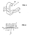
- Fig. 3 is a perspective view of a terminal for use in the connector;
- Fig. 4 is a cross-sectional view of a contact portion of the terminal;
- Fig. 5(A) is a front elevational view of the contact portion of the terminal;
- Fig. 5 (B) is a sectional view taken along line B-B of Fig. 5 (A);
- Fig. 5(C) is a sectional view taken along line C-C of Fig. 5 (A);
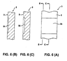
- Fig. 6(A) is a front elevational view of a contact portion according to another embodiment of the invention;
- Fig. 6 (B) is a sectional view taken along B-B of Fig. 6(A);
- Fig. 6(C) is a sectional view taken along C-C of Fig. 6(A); and
- Fig. 7 is a perspective sectional view of a conventional connector and a mating connector.
- A connector 1 includes a
housing 2 made of an insulative material andterminals 3 molded together with the housing 1 as a unit. Thehousing 2 has a peripheral wall 6 consisting of a pair of opposed longitudinal walls 4 and a pair ofopposed end walls 5. The peripheral wall 6 and a bottom wall 7 form acavity 2A for receiving a mating connector. Theterminal 3 is made by bending a metal strip in its thisknesswise direction to provide anengaging section 8 with acontact portion 8A for contact with a terminal of the mating connector and a connection section 9 projecting from the housing 1 for connection to a circuit board (not shown). - As shown in Fig. 2, the
terminal 3, which has such a shape as shown in Fig. 3, is molded with and supported by thehousing 2. - As shown in Fig. 3, the
terminal 3 is made by bending a metal strip in its thicknesswise direction to provide a substantially L-shaped form that has the verticalflat section 8 and the horizontal connection section 9. The end portion of thevertical section 8 is curved to provide acurved portion 10 which increases the retaining power of thehousing 2. Thiscurved portion 10 also assures smooth introduction of the terminal of a mating connector. Theengaging section 8 is level with the inside surface of the side wall 4 and is provided with an indentedcontact portion 8A. - As shown in Fig. 4, the
contact portion 8A is made of a curved surface that is a portion of cylinder having a radius R. The diameter 2R is greater than the width B of thecontact portion 8A so that thecontact portion 8A has the slope of a tangent 11A to theside edge 11 of theterminal 3. The tangent 12A to thecenter 12 of the width becomes parallel to the plane of theterminal 3. Thetangents 11A at bothside edges 11 and the tangent 12A at thecenter 12 share a common circle. Alternatively, thecontact portion 8A may be made of other surfaces such as three flat surfaces; two tangents to theside edges 11 and one tangent to thecenter 12. These flat surfaces may be connected with curved surfaces. The three tangents may contact different circles. - As shown in Figs. 5(A)-(C), the
contact portion 8A, which is made of a portion of cylinder, has sloped upper andlower end faces contact portion 8A becomes the maximum at the center and smaller toward the side edges so that the distance h becomes the maximum at the center and smaller toward the side edges. Consequently, the contact portion of a mating connector starts to contact the side edges at theupper end face 8B and moves to thecontact portion 8A for completing the contact. Thus, if the terminal of a mating connector is displaced in the widthwise direction, it is gradually moved toward the center for correction. - As shown in Figs. 6(A)-(C), the
contact portion 8A has no sloped transitional portions or end faces but stepped ones. Thecontact portion 8A becomes deeper toward the center so that after the mating terminal reaches thecontact portion 8A, it is guided in the widthwise direction. When the mating terminal moves to the stepped downcontact portion 8A, the operator obtains a click sense to know that the terminal reaches thecontact portion 8A. Both the connectors are locked at the stepped portions. The curved surface of thecontact portion 8A makes a point contact with the mating terminal, increasing the contact pressure to provide a reliable connection. - In. Fig. 2, the
mating connector 20 includes ahousing 21 having aperipheral wall 22 and a central wall 23 within a cavity defined by theperipheral wall 22 to provide aplugging cavity 24 for receiving the peripheral wall 6 of the connector 1. A plurality of terminals 25 are supported by theperipheral wall 22 and provided withcontact portions 25A arranged in theplugging cavity 24. Theterminal 24 is made by stamping a metal sheet to provide abase section 25B and a flexible arm 25C extending from thebase section 25B and having the contact portion orprojection 25A at its free end that is exposed in theplugging cavity 24. Afixing section 25D extends downward from thebase section 25B and press fitted into afixing slit 21A provided in thehousing 21 so that thehousing 21 supports the terminal 25. Aconnection section 25E extends laterally from thebase section 25B and is to be soldered to a circuit board P2. Themating connector 20 is not the subject matter of the application and its detailed description is omitted. That is, the mating connector may take a variety of structures. - The above connector is used as follows:
- (1) The
terminal 3 is pressed to provide anindented contact portion 8A after or before the metal strip is bent in its thicknesswise direction. - (2) When the
terminal 3 and thehousing 2 are molded together, the metal mold is in contact with side edges of thecontact portion 8A in the widthwise direction and the surface of thevertical section 8 in the longitudinal direction. Consequently, the side edges in the widthwise direction is level with the surface of thevertical section 8. The periphery of theindented contact portion 8A is in close contact with the metal mold so that no molten resin enters thecontact portion 8A. Even if there is a gap between the metal mold and the terminal at one of the side edges 11, the side edge of thecontact portion 8A is inclined gradually so that the gap is so small that no or little molten resin, which has a certain viscosity, enters thecontact portion 8A. - (3) As shown in Fig. 2, the connector 1 and the
mating connector 20 are connected to circuit boards P1 and P2, respectively, by soldering the connection sections 9 of theterminals 2 and theconnection sections 25E of the terminals 25 to the corresponding circuit portions of the circuit boards P1 and P2. - (4) The
mating connector 20 is plugged with the connector 1 from above. - (5) The
contact portion 25A of themating connector 20 is guided by thecurved portion 10 so as to slide on thevertical section 8 of theterminal 3. - (6) Then, the
contact portion 25A passes through the transitional portion orupper end face 8B into thecontact portion 8A of theterminal 3. If the terminal 25 is displaced laterally from the regular position, thecontact portion 25A begins contacting one of the sloped side edges of thecontact portion 8A and is guided toward the central area by the sloped surface. - (7) Thus, the mating terminal 25, even if displaced to either side, is brought into contact with the
contact portion 8A of theterminal 2 on both the sides without failure.
Claims (5)
- An electrical connector comprising:a housing made of an insulative material;a terminal made by bending a metal strop in its thicknesswise direction and molded together with said housing for support;a contact portion indented in said terminal so as to provide a curved longitudinal surface that extends from its side edges to its center, deepening gradually.
- The electrical connector according to claim 1, wherein said indented portion is made such that tangents to said side edges and a tangent to said bottom share a common circle having a diameter that is greater than a distance between said side edges.
- The electrical connector according to claim 2, wherein said indented portion made of an arc of said common circle in its widthwise direction.
- The electrical connector according to claim 1, wherein said indented portion has a sloped end face in its longitudinal direction, said sloped end face having a distance that increases from said side edge to said bottom center.
- The electrical connector according claim 1, wherein said indented portion has a stepped end face in its longitudinal direction.
Applications Claiming Priority (1)
| Application Number | Priority Date | Filing Date | Title |
|---|---|---|---|
| JP2006091349A JP4493101B2 (en) | 2006-03-29 | 2006-03-29 | Electrical connector |
Publications (3)
| Publication Number | Publication Date |
|---|---|
| EP1841021A2 true EP1841021A2 (en) | 2007-10-03 |
| EP1841021A3 EP1841021A3 (en) | 2008-12-17 |
| EP1841021B1 EP1841021B1 (en) | 2010-11-24 |
Family
ID=38146040
Family Applications (1)
| Application Number | Title | Priority Date | Filing Date |
|---|---|---|---|
| EP07005926A Ceased EP1841021B1 (en) | 2006-03-29 | 2007-03-22 | Electrical connector |
Country Status (5)
| Country | Link |
|---|---|
| US (1) | US7344386B2 (en) |
| EP (1) | EP1841021B1 (en) |
| JP (1) | JP4493101B2 (en) |
| CN (1) | CN100578864C (en) |
| TW (1) | TW200805800A (en) |
Families Citing this family (7)
| Publication number | Priority date | Publication date | Assignee | Title |
|---|---|---|---|---|
| JP4613235B2 (en) * | 2008-09-11 | 2011-01-12 | 日本航空電子工業株式会社 | connector |
| TWI396340B (en) * | 2009-07-31 | 2013-05-11 | Hon Hai Prec Ind Co Ltd | Electrical connector |
| JP2012018781A (en) * | 2010-07-07 | 2012-01-26 | Jst Mfg Co Ltd | Connector |
| JP5516678B2 (en) * | 2012-09-03 | 2014-06-11 | 第一精工株式会社 | Connector terminal |
| US8888506B2 (en) * | 2013-01-29 | 2014-11-18 | Japan Aviation Electronics Industry, Limited | Connector |
| WO2014132284A1 (en) * | 2013-02-27 | 2014-09-04 | パナソニック株式会社 | Connector, and header and socket, each being used for said connector |
| JP6537890B2 (en) * | 2014-09-26 | 2019-07-03 | 日本航空電子工業株式会社 | connector |
Family Cites Families (10)
| Publication number | Priority date | Publication date | Assignee | Title |
|---|---|---|---|---|
| DE69114748T2 (en) * | 1990-04-02 | 1996-06-05 | Whitaker Corp | Connectors mounted on a surface. |
| JPH10275662A (en) * | 1997-03-26 | 1998-10-13 | Whitaker Corp:The | Electrical connection method, electrical connection structure, electrical connector, and electronic circuit module between a pair of substrates |
| US6137063A (en) * | 1998-02-27 | 2000-10-24 | Micron Technology, Inc. | Electrical interconnections |
| US6024582A (en) * | 1999-08-12 | 2000-02-15 | Hon Hai Precision Ind. Co., Ltd. | Connection system |
| JP3368471B2 (en) * | 1999-10-25 | 2003-01-20 | 日本航空電子工業株式会社 | Electrical connector |
| JP3642705B2 (en) * | 1999-11-11 | 2005-04-27 | ヒロセ電機株式会社 | Electrical connector |
| JP2004103354A (en) * | 2002-09-09 | 2004-04-02 | Honda Tsushin Kogyo Co Ltd | Electrical connector |
| JP2005129255A (en) * | 2003-10-21 | 2005-05-19 | Three M Innovative Properties Co | Connector and connector system |
| JP4084292B2 (en) * | 2003-11-21 | 2008-04-30 | 日本圧着端子製造株式会社 | Pressure welding structure of coaxial cable |
| JP3726836B2 (en) * | 2004-08-02 | 2005-12-14 | 松下電工株式会社 | connector |
-
2006
- 2006-03-29 JP JP2006091349A patent/JP4493101B2/en not_active Expired - Lifetime
-
2007
- 2007-02-13 TW TW096105285A patent/TW200805800A/en not_active IP Right Cessation
- 2007-03-22 EP EP07005926A patent/EP1841021B1/en not_active Ceased
- 2007-03-27 CN CN200710089695.5A patent/CN100578864C/en active Active
- 2007-03-29 US US11/730,165 patent/US7344386B2/en active Active
Non-Patent Citations (1)
| Title |
|---|
| None |
Also Published As
| Publication number | Publication date |
|---|---|
| JP2007265888A (en) | 2007-10-11 |
| CN101047287A (en) | 2007-10-03 |
| CN100578864C (en) | 2010-01-06 |
| TW200805800A (en) | 2008-01-16 |
| US7344386B2 (en) | 2008-03-18 |
| EP1841021A3 (en) | 2008-12-17 |
| US20070232092A1 (en) | 2007-10-04 |
| EP1841021B1 (en) | 2010-11-24 |
| TWI360264B (en) | 2012-03-11 |
| JP4493101B2 (en) | 2010-06-30 |
Similar Documents
| Publication | Publication Date | Title |
|---|---|---|
| JP3860823B2 (en) | Connector and portable terminal equipped with this connector | |
| EP1841021B1 (en) | Electrical connector | |
| US7320606B2 (en) | Electrical connector with terminal having flat indentation | |
| US7976316B2 (en) | Electrical connector | |
| US7736177B2 (en) | Electrical connector having improved contacts therein | |
| US7845987B2 (en) | Electrical connector with plug connector and receptacle connector | |
| EP1434319A2 (en) | Coaxial electric connector | |
| US20120122332A1 (en) | Electrical connector assembly with contacts embedded in inner bottom of mating cavity | |
| US8500460B2 (en) | Board to board connectors and assembly thereof with contact-mounting wall having variable thickness | |
| US20140315442A1 (en) | Lower profile card edge connector | |
| US20060052008A1 (en) | Electrical connector with guidance face | |
| JP2001052785A (en) | Slider and connector including the same | |
| US20230069874A1 (en) | Male terminal fitting and terminal structure | |
| US6257900B1 (en) | Electrical connector with contacts having improved resiliency | |
| EP2028729A1 (en) | Connector for jack | |
| CN101322287A (en) | electrical connector | |
| JP2005293989A (en) | Terminal for electrical connection | |
| JP5457888B2 (en) | Card connector and card connector manufacturing method | |
| KR200471889Y1 (en) | Receptacle Terminal | |
| US20090298345A1 (en) | Connector | |
| JP3975222B2 (en) | Connector and portable terminal equipped with this connector | |
| JP2018022682A (en) | Receptacle connector and method of manufacturing receptacle connector | |
| US20050032438A1 (en) | Electrical connector | |
| JPH10264163A (en) | Insert mold and surface mount type connector using the same | |
| US7121861B2 (en) | Electrical card connector |
Legal Events
| Date | Code | Title | Description |
|---|---|---|---|
| PUAI | Public reference made under article 153(3) epc to a published international application that has entered the european phase |
Free format text: ORIGINAL CODE: 0009012 |
|
| AK | Designated contracting states |
Kind code of ref document: A2 Designated state(s): AT BE BG CH CY CZ DE DK EE ES FI FR GB GR HU IE IS IT LI LT LU LV MC MT NL PL PT RO SE SI SK TR |
|
| AX | Request for extension of the european patent |
Extension state: AL BA HR MK YU |
|
| PUAL | Search report despatched |
Free format text: ORIGINAL CODE: 0009013 |
|
| AK | Designated contracting states |
Kind code of ref document: A3 Designated state(s): AT BE BG CH CY CZ DE DK EE ES FI FR GB GR HU IE IS IT LI LT LU LV MC MT NL PL PT RO SE SI SK TR |
|
| AX | Request for extension of the european patent |
Extension state: AL BA HR MK RS |
|
| 17P | Request for examination filed |
Effective date: 20090617 |
|
| 17Q | First examination report despatched |
Effective date: 20090623 |
|
| AKX | Designation fees paid |
Designated state(s): FI GB |
|
| REG | Reference to a national code |
Ref country code: DE Ref legal event code: 8566 |
|
| GRAP | Despatch of communication of intention to grant a patent |
Free format text: ORIGINAL CODE: EPIDOSNIGR1 |
|
| GRAS | Grant fee paid |
Free format text: ORIGINAL CODE: EPIDOSNIGR3 |
|
| GRAA | (expected) grant |
Free format text: ORIGINAL CODE: 0009210 |
|
| AK | Designated contracting states |
Kind code of ref document: B1 Designated state(s): FI GB |
|
| REG | Reference to a national code |
Ref country code: GB Ref legal event code: FG4D |
|
| PLBE | No opposition filed within time limit |
Free format text: ORIGINAL CODE: 0009261 |
|
| STAA | Information on the status of an ep patent application or granted ep patent |
Free format text: STATUS: NO OPPOSITION FILED WITHIN TIME LIMIT |
|
| 26N | No opposition filed |
Effective date: 20110825 |
|
| PGFP | Annual fee paid to national office [announced via postgrant information from national office to epo] |
Ref country code: GB Payment date: 20180321 Year of fee payment: 12 Ref country code: FI Payment date: 20180312 Year of fee payment: 12 |
|
| PG25 | Lapsed in a contracting state [announced via postgrant information from national office to epo] |
Ref country code: FI Free format text: LAPSE BECAUSE OF NON-PAYMENT OF DUE FEES Effective date: 20190322 |
|
| GBPC | Gb: european patent ceased through non-payment of renewal fee |
Effective date: 20190322 |
|
| PG25 | Lapsed in a contracting state [announced via postgrant information from national office to epo] |
Ref country code: GB Free format text: LAPSE BECAUSE OF NON-PAYMENT OF DUE FEES Effective date: 20190322 |