EP1840754A2 - Information processing device - Google Patents
Information processing device Download PDFInfo
- Publication number
- EP1840754A2 EP1840754A2 EP07006542A EP07006542A EP1840754A2 EP 1840754 A2 EP1840754 A2 EP 1840754A2 EP 07006542 A EP07006542 A EP 07006542A EP 07006542 A EP07006542 A EP 07006542A EP 1840754 A2 EP1840754 A2 EP 1840754A2
- Authority
- EP
- European Patent Office
- Prior art keywords
- integrated circuit
- integrated circuits
- cpu
- slave
- user logic
- Prior art date
- Legal status (The legal status is an assumption and is not a legal conclusion. Google has not performed a legal analysis and makes no representation as to the accuracy of the status listed.)
- Withdrawn
Links
Images

Classifications
-
- G—PHYSICS
- G06—COMPUTING OR CALCULATING; COUNTING
- G06F—ELECTRIC DIGITAL DATA PROCESSING
- G06F15/00—Digital computers in general; Data processing equipment in general
- G06F15/16—Combinations of two or more digital computers each having at least an arithmetic unit, a program unit and a register, e.g. for a simultaneous processing of several programs
- G06F15/177—Initialisation or configuration control
-
- G—PHYSICS
- G06—COMPUTING OR CALCULATING; COUNTING
- G06F—ELECTRIC DIGITAL DATA PROCESSING
- G06F15/00—Digital computers in general; Data processing equipment in general
- G06F15/76—Architectures of general purpose stored program computers
- G06F15/78—Architectures of general purpose stored program computers comprising a single central processing unit
- G06F15/7867—Architectures of general purpose stored program computers comprising a single central processing unit with reconfigurable architecture
-
- G—PHYSICS
- G06—COMPUTING OR CALCULATING; COUNTING
- G06F—ELECTRIC DIGITAL DATA PROCESSING
- G06F15/00—Digital computers in general; Data processing equipment in general
- G06F15/76—Architectures of general purpose stored program computers
- G06F15/80—Architectures of general purpose stored program computers comprising an array of processing units with common control, e.g. single instruction multiple data processors
- G06F15/8007—Architectures of general purpose stored program computers comprising an array of processing units with common control, e.g. single instruction multiple data processors single instruction multiple data [SIMD] multiprocessors
- G06F15/8015—One dimensional arrays, e.g. rings, linear arrays, buses
Definitions
- the present invention generally relates to an information processing device.
- the present invention specifically relates to the information processing device that includes a plurality of integrated circuits that are interconnected via an external bus and each of which is structured to be connectable via an internal bus to a central processing unit (CPU), a user logic, and a bridge.
- CPU central processing unit
- FIG. 1 is a block diagram of the conventional information processing device that includes the plurality of integrated circuits, and it also depicts an outline of an address space.
- the conventional information processing device includes a plurality of (two) integrated circuits 10 and 20 that are interconnected via a synchronous communication line 30.
- the integrated circuit 10 includes a CPU 12 (22), a user logic 14 (24), and an internal bus 16 (26) that connects all these components.
- the integrated circuit 20 includes a CPU 22, a user logic 24, and an internal bus 26 that connects all these components. In this manner, when a plurality of integrated circuits 10 and 20 are used, to synchronize the parallel processing of both the CPUs 12 and 22, the synchronous communication line 30 connects the integrated circuits 10 and 20.
- a process is executed by the integrated circuit 10 and the integrated circuit 20 by reading respective computer programs stored in a program read only memory (ROM) 51 and a program ROM 52.
- ROM program read only memory
- Japanese Patent Laid-Open Application No. 2003-196251 discloses a technology in which, respective control programs to be executed by a plurality of CPUs are stored, in a batch, in a memory that is arranged on a common bus. Each CPU reads data through the same address at the same time an identifying register reads identifying data assigned to the data.
- ASIC Application Specific Integrated Circuit
- FPGA Field Programmable Gate Array
- VGA Video Graphics Array
- XGA Extended Graphics Array
- One approach could be to connect, corresponding to one CPU, a plurality of user logics on one integrated circuit board.
- each time number of user logics on the board is to be increased, it becomes necessary to change the design of the integrated circuit, and manufacture the new integrated circuit.
- this approach is not suitable for mass production.
- an information processing device includes a plurality of integrated circuits that are interconnected via an external bus.
- Each of the integrated circuits is structured to be connectable via an internal bus to a CPU, a user logic, and a bridge.
- the plurality of integrated circuits includes a master integrated circuit that controls other integrated circuits among the integrated circuits, and the other integrated circuit being slave integrated circuits with their CPUs being fixed to a reset state.
- the CPU of the master integrated circuit includes a user-logic control unit that controls the user logic of the slave integrated circuit via the external bus and the bridge of the slave integrated circuit; and an address managing unit that, when the user-logic control unit performs control of the user logic, manages a memory address space for the user logic of the slave integrated circuit as a separate memory space address.
- the information processing device generally has basic characteristics that are mentioned below.
- the information processing device includes a plurality of integrated circuits that are interconnected via an external bus.
- Each of the integrated circuits is structured to be connectable via an internal bus to a CPU, a user logic, and a bridge.
- one integrated circuit is set as a master integrated circuit that controls other integrated circuits, and the other integrated circuits are set as slave integrated circuits whose CPUs are fixed to a reset state.
- the CPU of the master integrated circuit controls user logics of the slave integrated circuits via the bridge and the external bus.
- user logic indicates a logical computing means that is realized by a user by using a particular logical circuit other than the CPU on an integrated circuit such as ASIC and FPGA. For example, it is possible to use an image computing unit as the user logic.
- the CPU of the master integrated circuit alone is used to control user logics of the integrated circuits and the CPU of the slave integrated circuits is fixed to a reset state. Therefore, one control program suffices the need and the control by the control program does not become complicated, resulting in an inexpensive formulation of the system. Furthermore, a communication line for synchronization of the master integrated circuit and the slave integrated circuits is not needed, and one ROM for storing control program is sufficient, which reduces expenditure on materials.
- the information processing device executes control by using a user logic control unit, it manages memory address space of the user logic of, the slave integrated circuits as a separate memory space.
- Fig. 2 is a block diagram of an example of the structure of the system applicable to the information processing device, and it also depicts an outline of memory address space. Only the relevant parts of the structure of the information processing device are depicted in the outline of the structure.
- a master integrated circuit 100 and a slave integrated circuit 200 connected via an external bus 400 so that signal an transmitted among the master integrated circuit 100 and the slave integrated circuit 200.
- the master integrated circuit 100 basically includes a CPU 102 that executes overall control on the information processing device; a user logic 104 that can be customized or has been customized by a user; an internal bus 106 that connects the CPU 102 and the user logic 104 with each other on the master integrated circuit 100; a bridge 108 that reads the address of data, which is on the external bus 400 or on the master integrated circuit 100, and judges sending/receiving of the corresponding data; and a M/S (Master/Slave) selecting port 110 that selects either the master integrated circuit or the slave integrated circuit according to the need.
- the M/S selecting port 110 of the master integrated circuit 100 is set to "master" position, so that the CPU 102 boots as usual.
- the CPU 102 is a device that conducts information processing by executing various processes according to control programs such as an operating system (OS) stored in a program ROM 501 or computer programs that specify procedures of various types of processes.
- the CPU 102 is set to control a plurality of the integrated circuits.
- the CPU 102 functions as the user logic control means that controls a user logic 204 via the external bus 400 and a bridge 208, and as an address managing means that manages memory space addresses other than those used by the user logic 104.
- the slave integrated circuit 200 includes a CPU 202; the user logic 204 that can be customized or has been customized by the user; an internal bus 206 that connects the CPU 202 and the user logic 204 with each other on the slave integrated circuit 200; the bridge 208 that reads the address of the data, which is on the external bus 400 or on the slave integrated circuit 200, and judges sending/receiving of the corresponding data; and a M/S (Master/Slave) selecting port 210 that selects either the master integrated circuit or the slave integrated circuit according to the need.
- the M/S selecting port 110 of the slave integrated circuit 200 is set to "slave" position, so that the CPU 202 is fixed to a reset state.
- a communication line for synchronization is arranged between the master integrated circuit 100 and the slave integrated circuit 200 to perform synchronization control.
- the communication line for synchronization which is necessary in the conventional technology for synchronizing parallel processing, is not needed.
- expenditure on materials is reduced.
- there is no need to develop a computer program for controlling synchronization which reduces the development cost as well.
- the external bus 400 shown in Fig. 2 has a function of connecting with each other the master integrated circuit 100, the slave integrated circuit 200, the program ROM 501, and other parts.
- the program ROM 501 stores the OS (operating system) and/or the computer programs that are used by the CPU 102 when performing various other processes
- a user logic control of controlling the user logic of the slave integrated circuit via the bridge and the external bus is explained below in detail.
- the CPU 102 Upon booting, the CPU 102 first judges whether the integrated circuit to which it belongs is the master integrated circuit or the slave integrated circuit. Because all the M/S selecting ports of the integrated circuits other than the master integrated circuit are set to "slave" position, and the CPUs in these integrated circuits are already in reset states, if a CPU boots normally, that CPU judges that it belongs to an integrated circuit that is the master integrated circuit.
- the CPU 102 sends, among the data to be processed by user logics, the data that is to be processed by the user logic 104 of the master integrated circuit 100 to the user logic 104 via the internal bus 106, and sends the data that is to be processed by the user logic 204 of the slave integrated circuit 200 to the user logic 204 via the bridge 208 and the external bus 400.
- the sequence or contents of the process is not limited to the example mentioned above, and can be applied in another way such as sending an upper part of the image processing data to the internal bus 106 and sending a lower part of the image processing data to the external bus 400. Further, it is also possible to send an asymmetrical data to each other, taking into consideration process speed and transmission rate.
- memory address space for the user logic of the slave integrated circuit is managed as a separate memory space address.
- the CPU 102 implements address management by treating the user logics of the master integrated circuit and the slave integrated circuit as if the user logics are on one substrate.
- the processing capacity of the user logic 104 expands by an amount equivalent to the processing capacity of the user logic 204, i.e., memory space available for allocation increases, which leads to prevention of allocation of identical addresses to different data (see lower part of Fig. 2).
- the address managing process is completed.
- the data that is allocated with addresses is processed according to an address offset process, and the data can be retrieved as image data that corresponds to the left or right position of the screen.
- the number of computer programs usually required for controlling is equal to the number of integrated circuits that are to be controlled.
- the information processing device formed as described above suffices with having one controlling program regardless of the number of the integrated circuits, which reduces the development expenditure.
- individual program ROMs are necessary for the number of integrated circuits.
- the information processing device formed as described above suffices with having one program ROM regardless of the number of the integrated circuits, which reduces the cost of materials.
- one CPU is able to control all of the integrated circuits, because of which, as compared to the initialization of a plurality of CPUs, there is no need to do adjustment among those CPUs, which results in simplification of the controlling process.
- each of the components of the configuration of the system that includes the master integrated circuit 100 and the slave integrated circuit 200 as shown in Fig. 2 are functional concepts, i.e., they are not necessarily physically configured as shown in the diagram.
- distribution and integration of the information processing device is not limited to the specific form shown in the diagram, all or part of it can functionally or physically be distributed or integrated based on arbitrary unit according to various types of loads.
Landscapes
- Engineering & Computer Science (AREA)
- Computer Hardware Design (AREA)
- Theoretical Computer Science (AREA)
- Physics & Mathematics (AREA)
- General Engineering & Computer Science (AREA)
- General Physics & Mathematics (AREA)
- Software Systems (AREA)
- Computing Systems (AREA)
- Image Processing (AREA)
- Memory System (AREA)
- Bus Control (AREA)
Abstract
Description
- The present invention generally relates to an information processing device. The present invention specifically relates to the information processing device that includes a plurality of integrated circuits that are interconnected via an external bus and each of which is structured to be connectable via an internal bus to a central processing unit (CPU), a user logic, and a bridge.
- A conventional information processing device that includes a plurality of integrated circuits is explained with reference to Fig. 1. Fig. 1 is a block diagram of the conventional information processing device that includes the plurality of integrated circuits, and it also depicts an outline of an address space.
- As shown in Fig. 1, the conventional information processing device includes a plurality of (two) integrated
circuits synchronous communication line 30. Theintegrated circuit 10 includes a CPU 12 (22), a user logic 14 (24), and an internal bus 16 (26) that connects all these components. Similarly, theintegrated circuit 20 includes a CPU 22, auser logic 24, and aninternal bus 26 that connects all these components. In this manner, when a plurality of integratedcircuits CPUs 12 and 22, thesynchronous communication line 30 connects the integratedcircuits - A process is executed by the
integrated circuit 10 and theintegrated circuit 20 by reading respective computer programs stored in a program read only memory (ROM) 51 and aprogram ROM 52. - As shown in Fig. 1, when both the CPUs (12, 22) control each of the user logics (14, 24) to execute the process, the CPUs (12, 22) use the same memory address space. An address managing method that can be employed when using the same memory address space is disclosed in
Japanese Patent Laid-Open Application No. 2003-196251 -
Japanese Patent Laid-Open Application No. 2003-196251 - However, in the information processing device disclosed in
Japanese Patent Laid-Open Application No. 2003-196251 - Particularly, in the integrated circuits of the information processing devices that are embedded in devices such as plasma displays, it is common to realize a user logic by using an Application Specific Integrated Circuit (ASIC), a Field Programmable Gate Array (FPGA) and the like to perform certain computational processing of a CPU, such as image computation function, that put a great burden on the CPU.
- In recent years, image display technology has improved from Video Graphics Array (VGA) to Extended Graphics Array (XGA) and further to full display; so that there is a problem that a great load is put on the conventional user logic for performing image processing. One approach could be to connect, corresponding to one CPU, a plurality of user logics on one integrated circuit board. However, in this approach, each time number of user logics on the board is to be increased, it becomes necessary to change the design of the integrated circuit, and manufacture the new integrated circuit. Thus, this approach is not suitable for mass production.
- Indecently, when plurality of integrated circuits, as in case of the integrated circuit device mentioned in
Japanese Patent Laid-Open Application No. 2003-196251 - It is an object of the present invention to at least partially solve the problems in the conventional technology.
- According to an aspect of the present invention, an information processing device includes a plurality of integrated circuits that are interconnected via an external bus. Each of the integrated circuits is structured to be connectable via an internal bus to a CPU, a user logic, and a bridge. The plurality of integrated circuits includes a master integrated circuit that controls other integrated circuits among the integrated circuits, and the other integrated circuit being slave integrated circuits with their CPUs being fixed to a reset state. The CPU of the master integrated circuit includes a user-logic control unit that controls the user logic of the slave integrated circuit via the external bus and the bridge of the slave integrated circuit; and an address managing unit that, when the user-logic control unit performs control of the user logic, manages a memory address space for the user logic of the slave integrated circuit as a separate memory space address.
- The above and other objects, features, advantages and technical and industrial significance of this invention will be better understood by reading the following detailed description of presently preferred embodiments of the invention, when considered in connection with the accompanying drawings.
-
- Fig. 1 is a block diagram of a conventional information processing device that includes plurality of integrated circuits, and it also depicts an outline of an address space; and
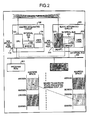
- Fig. 2 is a block diagram of an example of a structure of the system applicable to an information processing device according to an embodiment of the present invention, and it also depicts an outline of memory space.
- Exemplary embodiments of an information processing device according to the present invention are explained in detail with reference to the accompanying drawings; however, the invention is not limited to the embodiments.
- Particularly, the embodiment below is explained with respect to an application in the field of image processing technology; however, the embodiment can be applied to other fields in the same manner.
- General outline of the information processing device is explained below, and structure, process and the like of the information processing device are explained thereafter.
- The information processing device generally has basic characteristics that are mentioned below. In other words, the information processing device includes a plurality of integrated circuits that are interconnected via an external bus. Each of the integrated circuits is structured to be connectable via an internal bus to a CPU, a user logic, and a bridge. Among the plurality of integrated circuits, one integrated circuit is set as a master integrated circuit that controls other integrated circuits, and the other integrated circuits are set as slave integrated circuits whose CPUs are fixed to a reset state. The CPU of the master integrated circuit controls user logics of the slave integrated circuits via the bridge and the external bus.
- The term "user logic" as used herein indicates a logical computing means that is realized by a user by using a particular logical circuit other than the CPU on an integrated circuit such as ASIC and FPGA. For example, it is possible to use an image computing unit as the user logic.
- The CPU of the master integrated circuit alone is used to control user logics of the integrated circuits and the CPU of the slave integrated circuits is fixed to a reset state. Therefore, one control program suffices the need and the control by the control program does not become complicated, resulting in an inexpensive formulation of the system. Furthermore, a communication line for synchronization of the master integrated circuit and the slave integrated circuits is not needed, and one ROM for storing control program is sufficient, which reduces expenditure on materials.
- When the information processing device executes control by using a user logic control unit, it manages memory address space of the user logic of, the slave integrated circuits as a separate memory space.
- By managing memory address space of the user logic of the slave integrated circuits as separate memory address spaces, it becomes possible to prevent competition among memory address spaces.
- First, explanation is given about the structure of the system. Fig. 2 is a block diagram of an example of the structure of the system applicable to the information processing device, and it also depicts an outline of memory address space. Only the relevant parts of the structure of the information processing device are depicted in the outline of the structure. In this system, a master
integrated circuit 100 and a slaveintegrated circuit 200 connected via an external bus 400 so that signal an transmitted among the master integratedcircuit 100 and the slaveintegrated circuit 200. - As shown in Fig. 2, the master
integrated circuit 100 basically includes aCPU 102 that executes overall control on the information processing device; auser logic 104 that can be customized or has been customized by a user; aninternal bus 106 that connects theCPU 102 and theuser logic 104 with each other on the masterintegrated circuit 100; abridge 108 that reads the address of data, which is on the external bus 400 or on the master integratedcircuit 100, and judges sending/receiving of the corresponding data; and a M/S (Master/Slave) selectingport 110 that selects either the master integrated circuit or the slave integrated circuit according to the need. The M/S selecting port 110 of the master integratedcircuit 100 is set to "master" position, so that theCPU 102 boots as usual. - The
CPU 102 is a device that conducts information processing by executing various processes according to control programs such as an operating system (OS) stored in aprogram ROM 501 or computer programs that specify procedures of various types of processes. TheCPU 102 is set to control a plurality of the integrated circuits. Particularly, theCPU 102 functions as the user logic control means that controls auser logic 204 via the external bus 400 and abridge 208, and as an address managing means that manages memory space addresses other than those used by theuser logic 104. - The slave integrated
circuit 200 includes aCPU 202; theuser logic 204 that can be customized or has been customized by the user; an internal bus 206 that connects theCPU 202 and theuser logic 204 with each other on the slave integratedcircuit 200; thebridge 208 that reads the address of the data, which is on the external bus 400 or on the slave integratedcircuit 200, and judges sending/receiving of the corresponding data; and a M/S (Master/Slave) selectingport 210 that selects either the master integrated circuit or the slave integrated circuit according to the need. The M/S selecting port 110 of the slave integratedcircuit 200 is set to "slave" position, so that theCPU 202 is fixed to a reset state. - If the conventional technology is used, a communication line for synchronization is arranged between the master
integrated circuit 100 and the slave integratedcircuit 200 to perform synchronization control. However, in the slave integratedcircuit 200, because theCPU 202 is fixed to a reset state, the communication line for synchronization, which is necessary in the conventional technology for synchronizing parallel processing, is not needed. Thus, expenditure on materials is reduced. Furthermore, there is no need to develop a computer program for controlling synchronization, which reduces the development cost as well. - The external bus 400 shown in Fig. 2 has a function of connecting with each other the master integrated
circuit 100, the slave integratedcircuit 200, theprogram ROM 501, and other parts. - The
program ROM 501 stores the OS (operating system) and/or the computer programs that are used by theCPU 102 when performing various other processes - In the slave integrated
circuit 200, because the M/S selecting port 210 is set such that theCPU 202 set to a reset state, there is no need to have a program ROM corresponding to theCPU 202 for parallel processing, and a cost-cut can be realized as compared to the conventional device shown in Fig. 1. - An example of the system processing according to the embodiment is explained below in detail.
- A user logic control of controlling the user logic of the slave integrated circuit via the bridge and the external bus is explained below in detail.
- Upon booting, the
CPU 102 first judges whether the integrated circuit to which it belongs is the master integrated circuit or the slave integrated circuit. Because all the M/S selecting ports of the integrated circuits other than the master integrated circuit are set to "slave" position, and the CPUs in these integrated circuits are already in reset states, if a CPU boots normally, that CPU judges that it belongs to an integrated circuit that is the master integrated circuit. - The
CPU 102 sends, among the data to be processed by user logics, the data that is to be processed by theuser logic 104 of the master integratedcircuit 100 to theuser logic 104 via theinternal bus 106, and sends the data that is to be processed by theuser logic 204 of the slave integratedcircuit 200 to theuser logic 204 via thebridge 208 and the external bus 400. - For example, when the
CPU 102 is to control theuser logic 104 to process the data corresponding to right part of the screen out of the image processing data, and is to control theuser logic 204 to process the data corresponding to left part of the screen out of the image processing data, theCPU 102 sends the data corresponding to the right part to theinternal bus 106 and sends the data corresponding to the left part to the external bus 400. - With this, the user logic control process is completed. The sequence or contents of the process is not limited to the example mentioned above, and can be applied in another way such as sending an upper part of the image processing data to the
internal bus 106 and sending a lower part of the image processing data to the external bus 400. Further, it is also possible to send an asymmetrical data to each other, taking into consideration process speed and transmission rate. - Next, explanation is given in detail about an address managing process.
- When the
CPU 102 is to control processing according to the user logic control unit, memory address space for the user logic of the slave integrated circuit is managed as a separate memory space address. - For example, the
CPU 102 implements address management by treating the user logics of the master integrated circuit and the slave integrated circuit as if the user logics are on one substrate. In other words, as viewed from theCPU 102, the processing capacity of theuser logic 104 expands by an amount equivalent to the processing capacity of theuser logic 204, i.e., memory space available for allocation increases, which leads to prevention of allocation of identical addresses to different data (see lower part of Fig. 2). - With this, the address managing process is completed. As mentioned in the above example, the data that is allocated with addresses is processed according to an address offset process, and the data can be retrieved as image data that corresponds to the left or right position of the screen.
- In conventional information processing devices, the number of computer programs usually required for controlling is equal to the number of integrated circuits that are to be controlled. However, the information processing device formed as described above suffices with having one controlling program regardless of the number of the integrated circuits, which reduces the development expenditure. Further, usually individual program ROMs are necessary for the number of integrated circuits. However, the information processing device formed as described above suffices with having one program ROM regardless of the number of the integrated circuits, which reduces the cost of materials. Moreover, one CPU is able to control all of the integrated circuits, because of which, as compared to the initialization of a plurality of CPUs, there is no need to do adjustment among those CPUs, which results in simplification of the controlling process.
- The embodiments according to the present invention are explained above; however, the present invention is applicable to embodiments other than the embodiments mentioned above, and also to any other embodiments that come under the scope of the technological, philosophy of the claims.
- Particularly, in the embodiments mentioned above, an example is described of a combination of one master integrated circuit with one slave integrated circuit. However, it need not be limited to the example, and one master integrated circuit can be in combination with more than two slave integrated circuits.
- In addition, process steps, control steps, specific nomenclature mentioned in the specification and the diagrams can be arbitrarily changed if not otherwise specified.
- Furthermore, each of the components of the configuration of the system that includes the master integrated
circuit 100 and the slave integratedcircuit 200 as shown in Fig. 2 are functional concepts, i.e., they are not necessarily physically configured as shown in the diagram. - Moreover, distribution and integration of the information processing device is not limited to the specific form shown in the diagram, all or part of it can functionally or physically be distributed or integrated based on arbitrary unit according to various types of loads.
- Although the invention has been described with respect to a specific embodiment for a complete and clear disclosure, the appended claims are not to be thus limited but are to be construed as embodying all modifications and alternative constructions that may occur to one skilled in the art that fairly fall within the basic teaching herein set forth.
Claims (1)
- An information processing device comprising a plurality of integrated circuits (100, 200) that are interconnected via an external bus (400), each of the integrated circuits (100, 200) being structured to be connectable via an internal bus (106, 206) to a CPU (102, 202), a user logic (104, 204), and a bridge (108, 208), whereinthe plurality of integrated circuits (100, 200) including a master integrated circuit (100) that controls other integrated circuits among the integrated circuits, and the other integrated circuit being slave integrated circuits (200) with their CPUs (202) being fixed to a reset state, the CPU (102) of the master integrated circuit (100) includinga user-logic control unit that controls the user logic (204) of the slave integrated circuit (200) via the external bus (400) and the bridge (208) of the slave integrated circuit (200); andan address managing unit that, when the user-logic control unit performs control of the user logic (204), manages a memory address space for the user logic (204) of the slave integrated circuit (200) as a separate memory space address.
Applications Claiming Priority (1)
| Application Number | Priority Date | Filing Date | Title |
|---|---|---|---|
| JP2006094732A JP2007272358A (en) | 2006-03-30 | 2006-03-30 | Information processor |
Publications (2)
| Publication Number | Publication Date |
|---|---|
| EP1840754A2 true EP1840754A2 (en) | 2007-10-03 |
| EP1840754A3 EP1840754A3 (en) | 2009-07-08 |
Family
ID=38353404
Family Applications (1)
| Application Number | Title | Priority Date | Filing Date |
|---|---|---|---|
| EP07006542A Withdrawn EP1840754A3 (en) | 2006-03-30 | 2007-03-29 | Information processing device |
Country Status (3)
| Country | Link |
|---|---|
| US (1) | US20070288722A1 (en) |
| EP (1) | EP1840754A3 (en) |
| JP (1) | JP2007272358A (en) |
Families Citing this family (1)
| Publication number | Priority date | Publication date | Assignee | Title |
|---|---|---|---|---|
| KR102830966B1 (en) * | 2019-12-16 | 2025-07-07 | 주식회사 엘엑스세미콘 | Method for writing firmware |
Family Cites Families (8)
| Publication number | Priority date | Publication date | Assignee | Title |
|---|---|---|---|---|
| US5584034A (en) * | 1990-06-29 | 1996-12-10 | Casio Computer Co., Ltd. | Apparatus for executing respective portions of a process by main and sub CPUS |
| US5603055A (en) * | 1994-01-27 | 1997-02-11 | Vlsi Technology, Inc. | Single shared ROM for storing keyboard microcontroller code portion and CPU code portion and disabling access to a portion while accessing to the other |
| US5784636A (en) * | 1996-05-28 | 1998-07-21 | National Semiconductor Corporation | Reconfigurable computer architecture for use in signal processing applications |
| US5887138A (en) * | 1996-07-01 | 1999-03-23 | Sun Microsystems, Inc. | Multiprocessing computer system employing local and global address spaces and COMA and NUMA access modes |
| DE19832060C2 (en) * | 1998-07-16 | 2000-07-06 | Siemens Ag | Duplicate processor device |
| JP3481485B2 (en) * | 1999-01-28 | 2003-12-22 | エヌイーシーコンピュータテクノ株式会社 | Multiprocessor system |
| KR20030029913A (en) * | 2001-07-07 | 2003-04-16 | 코닌클리즈케 필립스 일렉트로닉스 엔.브이. | Processor cluster |
| US20040215991A1 (en) * | 2003-04-23 | 2004-10-28 | Dell Products L.P. | Power-up of multiple processors when a voltage regulator module has failed |
-
2006
- 2006-03-30 JP JP2006094732A patent/JP2007272358A/en active Pending
-
2007
- 2007-03-29 US US11/730,198 patent/US20070288722A1/en not_active Abandoned
- 2007-03-29 EP EP07006542A patent/EP1840754A3/en not_active Withdrawn
Also Published As
| Publication number | Publication date |
|---|---|
| US20070288722A1 (en) | 2007-12-13 |
| EP1840754A3 (en) | 2009-07-08 |
| JP2007272358A (en) | 2007-10-18 |
Similar Documents
| Publication | Publication Date | Title |
|---|---|---|
| JP6321221B2 (en) | Control module for resource management of multiple mixed signals | |
| US7062578B2 (en) | Flexible processing hardware architecture | |
| US20110185163A1 (en) | Multi-root pci express switch, boot method thereof, and multi-root pci manager program | |
| US6295566B1 (en) | PCI add-in-card capability using PCI-to-PCI bridge power management | |
| EP1938190B1 (en) | Method and apparatus to clear semaphore reservation | |
| US10002103B2 (en) | Low-pin microcontroller device with multiple independent microcontrollers | |
| WO2009120187A2 (en) | System and method for transforming pcie sr-iov functions to appear as legacy functions | |
| US20060123282A1 (en) | Service layer architecture for memory access system and method | |
| CN114035842B (en) | Firmware configuration method, computing system configuration method, computing device and equipment | |
| JPH11126182A (en) | Computer bus communication device and method thereof | |
| CN107743621B (en) | IC input and output | |
| EP0463775B1 (en) | Multiple speed expansion card | |
| US20070288722A1 (en) | Information processing device | |
| US8423693B2 (en) | Circuit and method for pipe arbitration using available state information and arbitration | |
| US5159674A (en) | Method for supplying microcommands to multiple independent functional units having a next microcommand available during execution of a current microcommand | |
| US20240220436A1 (en) | Supporting multiple controller circuits on a multiplexed communication bus | |
| JPH0855097A (en) | Data processing system and memory access method thereof | |
| US9213663B2 (en) | Output input control apparatus and control method thereof | |
| US6253233B1 (en) | Multi-cut system | |
| US7565456B2 (en) | Method for reconfiguring an automation device | |
| WO2023106073A1 (en) | Onboard device, program, and information processing method | |
| JP3743601B2 (en) | Information transfer mediation device | |
| JP2007102544A (en) | Digital signal processor system and boot method thereof. | |
| KR19980070351A (en) | Programmable controller | |
| CA2392503A1 (en) | Computer module and motherboard |
Legal Events
| Date | Code | Title | Description |
|---|---|---|---|
| PUAI | Public reference made under article 153(3) epc to a published international application that has entered the european phase |
Free format text: ORIGINAL CODE: 0009012 |
|
| AK | Designated contracting states |
Kind code of ref document: A2 Designated state(s): AT BE BG CH CY CZ DE DK EE ES FI FR GB GR HU IE IS IT LI LT LU LV MC MT NL PL PT RO SE SI SK TR |
|
| AX | Request for extension of the european patent |
Extension state: AL BA HR MK YU |
|
| PUAL | Search report despatched |
Free format text: ORIGINAL CODE: 0009013 |
|
| AK | Designated contracting states |
Kind code of ref document: A3 Designated state(s): AT BE BG CH CY CZ DE DK EE ES FI FR GB GR HU IE IS IT LI LT LU LV MC MT NL PL PT RO SE SI SK TR |
|
| AX | Request for extension of the european patent |
Extension state: AL BA HR MK RS |
|
| RIC1 | Information provided on ipc code assigned before grant |
Ipc: G06F 9/38 20060101ALI20090602BHEP Ipc: G06F 15/80 20060101AFI20090602BHEP |
|
| AKX | Designation fees paid | ||
| STAA | Information on the status of an ep patent application or granted ep patent |
Free format text: STATUS: THE APPLICATION IS DEEMED TO BE WITHDRAWN |
|
| 18D | Application deemed to be withdrawn |
Effective date: 20100109 |
|
| REG | Reference to a national code |
Ref country code: DE Ref legal event code: 8566 |