EP1837947A1 - Dielectric resonator device, oscillator device and transmitting/receiving device - Google Patents
Dielectric resonator device, oscillator device and transmitting/receiving device Download PDFInfo
- Publication number
- EP1837947A1 EP1837947A1 EP05819851A EP05819851A EP1837947A1 EP 1837947 A1 EP1837947 A1 EP 1837947A1 EP 05819851 A EP05819851 A EP 05819851A EP 05819851 A EP05819851 A EP 05819851A EP 1837947 A1 EP1837947 A1 EP 1837947A1
- Authority
- EP
- European Patent Office
- Prior art keywords
- coupling
- mode resonator
- dielectric
- electrodes
- electrode
- Prior art date
- Legal status (The legal status is an assumption and is not a legal conclusion. Google has not performed a legal analysis and makes no representation as to the accuracy of the status listed.)
- Granted
Links
Images










Classifications
-
- H—ELECTRICITY
- H01—ELECTRIC ELEMENTS
- H01P—WAVEGUIDES; RESONATORS, LINES, OR OTHER DEVICES OF THE WAVEGUIDE TYPE
- H01P7/00—Resonators of the waveguide type
- H01P7/10—Dielectric resonators
-
- H—ELECTRICITY
- H01—ELECTRIC ELEMENTS
- H01P—WAVEGUIDES; RESONATORS, LINES, OR OTHER DEVICES OF THE WAVEGUIDE TYPE
- H01P7/00—Resonators of the waveguide type
- H01P7/08—Strip line resonators
- H01P7/082—Microstripline resonators
-
- H—ELECTRICITY
- H03—ELECTRONIC CIRCUITRY
- H03B—GENERATION OF OSCILLATIONS, DIRECTLY OR BY FREQUENCY-CHANGING, BY CIRCUITS EMPLOYING ACTIVE ELEMENTS WHICH OPERATE IN A NON-SWITCHING MANNER; GENERATION OF NOISE BY SUCH CIRCUITS
- H03B5/00—Generation of oscillations using amplifier with regenerative feedback from output to input
- H03B5/18—Generation of oscillations using amplifier with regenerative feedback from output to input with frequency-determining element comprising distributed inductance and capacitance
- H03B5/1864—Generation of oscillations using amplifier with regenerative feedback from output to input with frequency-determining element comprising distributed inductance and capacitance the frequency-determining element being a dielectric resonator
- H03B5/187—Generation of oscillations using amplifier with regenerative feedback from output to input with frequency-determining element comprising distributed inductance and capacitance the frequency-determining element being a dielectric resonator the active element in the amplifier being a semiconductor device
- H03B5/1876—Generation of oscillations using amplifier with regenerative feedback from output to input with frequency-determining element comprising distributed inductance and capacitance the frequency-determining element being a dielectric resonator the active element in the amplifier being a semiconductor device the semiconductor device being a field-effect device
Definitions
- the present invention relates to dielectric resonance apparatuses, which oscillate high-frequency electro-magnetic waves such as microwaves and millimeter waves, oscillation apparatuses using the dielectric resonance apparatuses, and transmission/reception apparatuses.
- a known dielectric resonance apparatus includes a resonator having a circular electrode on a surface of a dielectric substrate and power-supply lines which are arranged on the dielectric substrate and which are arranged in the vicinity of ends of the resonator (refer to, for example, Patent Document 1).
- a known oscillation apparatus using a dielectric resonance apparatus includes an oscillator block which oscillates signals having predetermined oscillation frequencies and a dielectric resonator block constituted by a TM010-mode resonator used for setting the oscillation frequencies (refer to, for example, Patent Document 2).
- the oscillator block and the dielectric resonator block are separately configured using dielectric substrates.
- dielectric constants and the thicknesses of the dielectric substrates are suitably set for the oscillator block and the dielectric resonator block. Accordingly, a substrate having a low dielectric constant is used for the oscillator block, for example, whereby accuracy of dimension is relatively enhanced.
- a substrate having a high dielectric constant and a large thickness is used for the dielectric resonator block, whereby Q factor is enhanced. Furthermore, mass production of the oscillator apparatus is facilitated by using of the oscillator block and the resonator block in combination.
- a known waveguide dielectric resonator includes a substantially cuboid dielectric block (refer to, for example, Patent Document 3).
- a dielectric resonator includes an input/output electrode having a short-circuit point connected to a ground electrode so as to face a surface on which the dielectric block is implemented. Furthermore, the dielectric resonator is excited using the input/output electrode.
- a distance between each of the power-supply lines and the ground is set larger than a distance between the resonator and the ground so that the power-supply lines and the resonator are strongly coupled with each other.
- the thickness of the dielectric resonance apparatus tends to be large.
- the power-supply lines are arranged outside of the resonator, the area of the dielectric resonance apparatus also tends to be large. Accordingly, the size of the dielectric resonance apparatus is increased.
- a frequency control circuit for controlling an oscillation frequency and a terminating resistor are arranged on the dielectric substrate of the dielectric resonator block.
- the dielectric substrate used for the dielectric resonator block has a high dielectric constant, the cost tends to be increased, and furthermore, the area of the dielectric substrate tends to be increased. This leads to the problem that production cost of the oscillation apparatus is increased.
- an input/output electrode is arranged on the dielectric block which should be subjected to high-accuracy outer-shape processing, even if the dielectric block and the input/output electrode is slightly displaced with respect to each other, an amount of coupling between the dielectric resonator and the input/output electrode is changed. Consequently, variation of amounts of coupling between individual dielectric resonators and corresponding input/output electrodes is likely to be generated, and variation of electric characteristics of the resonators becomes large.
- the dielectric resonance apparatus is miniaturized and has a stable coupling characteristic, an oscillation apparatus and a transmission/reception apparatus using the dielectric resonance apparatus may be made compact while stable characteristics thereof are achieved.
- a TM010-mode resonator 1 includes a dielectric substrate 2, a substantially circular electrode 3, and a back-surface electrode 7, which will be described later.
- the dielectric substrate 2 has a plate shape (a chip shape) and is made of a dielectric material.
- the dielectric substrate 2 is a substantially square plate having sides of length L1 in the X direction (vertical direction) and Y direction (horizontal direction) and having a thickness T1 in the Z direction (thickness direction).
- the substantially circular electrode 3 is disposed on a surface 2A of the dielectric substrate 2.
- the substantially circular electrode 3 is made of a dielectric thin film using a metal material, for example, and disposed in a center of the dielectric substrate 2.
- the substantially circular electrode 3 has a diameter of D which is defined in accordance with a resonance frequency of the dielectric substrate 2.
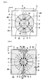
- the substantially circular electrode 3 has four cutout portions 4 radially formed therein.
- the four cutout portions 4 are arranged with equal intervals in a circumferential direction and each of the four cutout portions 4 has a groove shape and extends along the radial direction and is used for setting a resonance frequency for other resonance modes (for example, a TM210 mode, and a TM310 mode).
- a coupling line 5 is included in a magnetic-field coupling section.
- the coupling line 5 is arranged on a back surface 2B of the dielectric substrate 2 so as to face the substantially circular electrode 3 and extends toward an end portion (an end face 2C) of the dielectric substrate 2.
- the coupling line 5 linearly extends through a center axis O of the substantially circular electrode 3 and extends along the diameter of the substantially circular electrode 3.
- the coupling line 5 has a predetermined width W1.
- connection portions 6 having a width W2 which is larger than the width W1 are arranged at opposite ends of the coupling line 5 for facilitating the connection between the coupling line 5 and signal lines 11 which will be described later.
- connection portions 6 has a width of W2 and a length of L2, which is of a value equal to a value of the width of W2, so as to have a substantially square shape, for example, and is connected to one of the signal lines 11 disposed on an external substrate 10 which will be described later.
- the two back-surface electrodes 7 are disposed on the back surface 2B of the dielectric substrate 2 and disposed on either side of the coupling line 5 in the width direction of the coupling line 5.
- the two back-surface electrodes 7 cover the entire back surface 2B of the dielectric substrate 2 except for portions in the vicinity of the end face 2C of the dielectric substrate 2, and face the substantially circular electrode 3 with the dielectric substrate 2 interposed therebetween.
- a frame portion 8 having a width of ⁇ 0 is formed between the back-surface electrode 7 and the end face 2C of the dielectric substrate 2.
- the dielectric substrate 2 is exposed through the frame portion 8.
- Gap 9 is formed between the back-surface electrodes 7 and the coupling line 5.
- the gap 9 linearly extends along the coupling line 5 and the gap 9 has a width of ⁇ 1.
- the gap 9 functions as an insulator arranged between the back-surface electrodes 7 and the coupling line 5.
- the width of the gap 9 is set to ⁇ 2 between the back-surface electrodes 7 and the connection portions 6.
- the TM010-mode resonator 1 is implemented on the external substrate 10.
- the external substrate 10 has a plate shape having a predetermined thickness T0.
- the TM010-mode resonator 1 is disposed on a surface of the external substrate 10 such that the back surface 2B of the dielectric substrate 2 faces the surface of the external substrate 10.
- the signal lines 11 and ground electrodes 13, which will be described later, are disposed on the surface of the external substrate 10 at any portions except for portions where the surface of the external substrate 10 faces the coupling line 5 of the TM010-mode resonator 1.
- the two signal lines 11 are arranged on the surface of the external substrate 10.
- the signal lines 11 are arranged in positions different from positions where the TM010-mode resonator 1 faces the coupling line 5, and linearly extend along an imaginary line extending from the ends of the coupling line 5.
- Connection portions 12 are arranged at end portions of the signal lines 11 so as to face the connection portions 6 of the coupling line 5.
- the connection portions 12 of the signal lines 11 are superposed with the connection portions 6 of the coupling line 5 so that the TM010-mode resonator 1 and the external substrate 10 are connected with each other using bumps 15 which will be described later.
- the two ground electrodes 13 are disposed on the surface of the external substrate 10 such that the ground electrodes 13 are insulated from the signal lines 11.
- the two ground electrodes 13 are separately arranged in the width direction of the TM010-mode resonator 1 with a portion on the external substrate 10 facing the coupling line 5 of the TM010-mode resonator 1 interposed therebetween.
- the ground electrodes 13 are connected to ground electrodes (not shown) formed on a back surface of the external substrate 10 through via holes 14.
- the ground electrodes 13 are connected to the back-surface electrodes 7 of the TM010-mode resonator 1 using the bumps 15.
- the bumps 15 are used to connect the external substrate 10 and the TM010-mode resonator 1 with each other.
- Each of the bumps 15 has a substantially cylindrical shape having a diameter of ⁇ and a height of h, and is used for connecting the connection portions 12 of the signal lines 11 and the connection portions 6 of the coupling line 5, and connecting the ground electrodes 13 and the back-surface electrodes 7.
- the bumps 15 are projected from the surface of the external substrate 10 and support the TM010-mode resonator 1.
- the dielectric resonance apparatus according to the embodiment has the configuration as described above, and operation thereof will now be described.
- an electric field E is generated inside the dielectric substrate 2, that is, between the substantially circular electrode 3 and the back-surface electrodes 7 in the thickness direction of the dielectric substrate 2.
- a circular magnetic field H which concentrically rotates in an XY plane along the circumference of the substantially circular electrode 3 which is a concentric circle.
- a magnitude of the circular magnetic field H is small in the vicinity of an axis O of the substantially circular electrode 3 and in the vicinity of an outer circumference edge whereas a magnitude of the circular magnetic field H is large in an intermediate region (an intermediate region in a radial direction) between the axis P and the outer circumference edge.
- the high-frequency signal When a high-frequency signal is supplied to the signal lines 11 of the external substrate 10, the high-frequency signal is supplied from the signal lines 11 to the coupling line 5 of the TM010-mode resonator 1, and thereby generates a magnetic field H0 which rotates around the coupling line 5 in a YZ plane.
- the dielectric resonance apparatus may be shown as an equivalent circuit illustrated in Fig. 8, and the coupling line 5 functions as a strip line and is magnetically coupled with the TM010-mode resonator 1. Accordingly, a reaction resonator may be formed by setting one end of the coupling line 5 as a terminal end.
- a reaction resonator employing the dielectric resonance apparatus according to the embodiment is analyzed in terms of a reflection characteristic using an electro-magnetic field simulation.
- Fig. 9 shows the result of the analysis.
- the result of the analysis shown in Fig. 9 is obtained when the one end of the coupling line 5 is set as a terminal end and a reflection amount with respect to a frequency characteristic of the TM010-mode resonator 1 viewed from the other end of the coupling line 5 is calculated.
- the dielectric substrate 2 has a length L1 of 1.94 mm, a thickness T1 of 0.30 mm, and a relative dielectric constant ⁇ r1 of 26.
- the substantially circular electrode 3 has a diameter D of 1.56 mm, and each of the cutout portions 4 has a groove width ⁇ p of 0.04 mm, and a groove length Lp of 0.35 mm.
- the coupling line 5 has a width W1 of 0.08 mm
- each of the connection portions 6 has a width W2 and a length L2 of 0.15 mm
- a portion between the coupling line 5 and the back-surface electrodes 7 in the gap 9 has a width ⁇ 0 of 0.030 mm
- a portion between the connection portions 6 and the back-surface electrodes 7 in the gap 9 has a width ⁇ 2 of 0.025 mm
- the frame portion 8 has a width ⁇ 0 of 0.05 mm.
- the external substrate 10 has a thickness T0 of 0.20 mm, a relative dielectric constant ⁇ r0 of 10, and a characteristic impedance Z0 of 50 ⁇ .
- Each of the bumps 15 has a diameter ⁇ of 0.09 mm and a height h of 0.04 mm.
- a reaction resonator in which an amount of reflection thereof is large around the resonant frequency band of the TM010-mode resonator 1, may be configured utilizing the dielectric resonance apparatus according to this embodiment.
- the coupling line 5 connected to the signal lines 11 is arranged on the back surface 2B of the dielectric substrate 2 of the TM010-mode resonator 1, the magnetic field H0 generated in the coupling line 5 is made to coincide with the circular magnetic field H generated in the TM010-mode resonator 1 whereby the coupling line 5 is magnetically coupled with the TM010-mode resonator 1. Accordingly, the TM010-mode resonator 1 and the signal lines 11 are connected with each other using the coupling line 5, and the TM010-mode resonator 1 is excited by a high-frequency signal supplied to the signal lines 11.
- the TM010-mode resonator 1 may be easily connected to the external substrate 10 through the bumps 15. Furthermore, since the coupling line 5 serving as a magnetic-field coupling section is arranged on the back surface 2B of the dielectric substrate 2 of the TM010-mode resonator 1, when compared with a case where a magnetic-field coupling section is arranged on the external substrate 10, a variation of an amount of coupling between the TM010-mode resonator 1 and the coupling line 5 may be reduced, and a electrical characteristic of the TM010-mode resonator 1 may be kept substantially constant.
- the TM010-mode resonator 1 may be made smaller when compared with a case where the coupling line 5 is arranged in a position facing the outside of the substantially circular electrode 3.
- the coupling line 5 arranged on the back surface 2B of the dielectric substrate 2 serves as a magnetic-field coupling section, the coupling line 5 may be formed simultaneously (together) with the back-surface electrodes 7 included in the TM010-mode resonator 1. Accordingly, a variation of an amount of coupling between the TM010-mode resonator 1 and the coupling line 5 may be reduced and an electrical characteristic of the TM010-mode resonator 1 may be kept constant.
- the TM010-mode resonator 1 may be made smaller when compared with a case where the coupling line 5 is magnetically coupled with the TM010-mode resonator 1 in a position facing the outside of the substantially circular electrode 3.
- an electrical characteristic of the TM010-mode resonator 1 is determined in accordance with the substantially circular electrode 3 and the back-surface electrodes 7 and the thickness T1 of the dielectric substrate 2, which constitute the TM010-mode resonator 1. Accordingly, since the coupling line 5 is simultaneously formed with the back-surface electrodes 7, a stable coupling characteristic may be easily obtained. As a result, a fabrication cost may be reduced when compared with a case where a waveguide dielectric resonance apparatus for which high-accuracy processing is difficult is employed.
- the coupling line 5 has a stable coupling characteristic with respect to the TM010-mode resonator 1
- a frequency control circuit and the like need not be arranged on the dielectric substrate 2 of the TM010-mode resonator 1, but may be arranged on the external substrate 10. Since the frequency control circuit may be removed from the dielectric substrate 2, the TM010-mode resonator 1 may be miniaturized.
- the coupling line 5, which is arranged at the position facing the substantially circular electrode 3, serves as a magnetic-field coupling section, and opposite ends thereof are connected to the signal lines 11 arranged on the external substrate 10. Therefore, in this configuration, the TM010-mode resonator 1 is connected in parallel to a circuit arranged on the external substrate 10 having the signal lines 11 thereon.
- the magnetic field H0 having a direction the same as that of the circular magnetic field H generated in the dielectric substrate 2 of the TM010-mode resonator 1 is generated around the coupling line 5 by supplying a high-frequency signal having a frequency serving as a resonant frequency to the coupling line 5.
- the coupling line 5 and the TM010-mode resonator 1 are magnetically coupled with each other, the high-frequency signal supplied from one of the opposite ends of the coupling line 5 is reflected by the TM010-mode resonator 1. Consequently, a reaction resonator is constituted and a degree of freedom of design of an oscillation apparatus, for example, is enhanced.
- a current loss due to existence of the coupling line 5 may be reduced when compared with a case where the coupling line 5 is arranged in any other position. That is, when the TM010-mode resonator 1 is made to resonate, as shown in Fig. 6, a resonant current I is radially supplied toward the axis O of the substantially circular electrode 3.
- the coupling line 5 is arranged so as to pass through a position other than the axis O of the substantially circular electrode 3
- the resonant current I is interrupted by the gap 9 arranged so as to surround both sides of the coupling line 5
- a current loss of the TM010-mode resonator 1 is increased.
- the coupling line 5 is arranged so as to pass through the axis O of the substantially circular electrode 3
- the resonant current I is not interrupted by the gap 9 and a current loss due to the existence of the coupling line 5 is reduced.
- the signal lines 11 and the ground electrodes 13 are arranged in a region on the external substrate 10 except for a region on the external substrate 10 where the external substrate 10 faces the coupling line 5, when the TM010-mode resonator 1 is implemented on the external substrate 10, the ground electrodes 13 on the external substrate 10 and the like are not arranged around the coupling line 5. Accordingly, even if a variation in the height h of the bumps 15 is generated when the coupling line 5 and the back-surface electrodes 7 on the TM010-mode resonator 1 are connected to the signal lines 11 and the ground electrodes 13 on the external substrate 10, respectively, using the bumps 15, the magnetic field H0 generated around the coupling line 5 is not influenced by the ground electrodes 13 of the external substrate 10. Consequently, even if the variation of the heights h of the bumps 15 is generated, an amount of coupling between the TM010-mode resonator 1 and the coupling line is kept constant, that is, stable coupling is achieved.
- the gap 9 is arranged in the width direction of the coupling line 5 so as to surround the coupling line 5, the magnetic field H0 generated around the coupling line 5 in accordance with the width ⁇ 1 of the gap 9 is changed, and the amount of coupling between the coupling line 5 and the TM010-mode resonator 1 is changed.
- the width ⁇ 1 of the gap 9 is set to various values, and a reaction resonator employing the dielectric resonance apparatus according to the embodiment is analyzed in terms of a reflection characteristic using a electro-magnetic field simulation similarly to Fig. 9.
- Fig. 10 shows the result of the analysis.
- the various values of the width ⁇ 1 of the gap 9 include 0.02 mm, 0.03 mm, and 0.04 mm. Parameters other than the width ⁇ 1 of the gap 9 are set to the same values as those where the result shown in Fig. 9 is obtained.
- the axis of abscissa in Fig. 10 illustrates a normalized frequency, which is normalized using a resonant frequency.
- the magnetic field H0 generated around the coupling line 5 is expanded and therefore an amount of coupling is increased by setting a value of the width ⁇ 1 of the gap 9 larger, whereas the magnetic field H0 generated around the coupling line 5 is reduced and therefore an amount of coupling is reduced by setting the value of the width ⁇ 1 of the gap 9 smaller. Accordingly, the amount of coupling between the coupling line 5 and the TM010-mode resonator 1 may be controlled to a desired value. A degree of freedom of design is enhanced.
- the amount of coupling between the coupling line 5 and the TM010-mode resonator 1 is set to a desired value in accordance with the width ⁇ 1 of the gap 9.
- the amount of coupling between the coupling line 5 and the TM010-mode resonator 1 may be set to the desired value in accordance with the width W1 of the coupling line 5.
- the magnetic field generated around the coupling line 5 is expanded and therefore an amount of coupling is increased by setting a value of the width W1 of the coupling line 5 larger, whereas the magnetic field generated around the coupling line 5 is reduced and therefore an amount of coupling is reduced by setting the value of the width W1 of the coupling line 5 smaller.
- the four cutout portions 4 are arranged on the substantially circular electrode 3 for controlling a resonant frequency for other resonance modes.
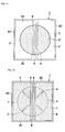
- a substantially circular electrode 3' without cutout portions may be employed.
- a shape of the substantially circular electrode 3 is not limited to the circular shape but may be an oval shape.
- connection portions 6, each of which has a large width are arranged on either side of the coupling line 5.
- connection portions may be eliminated and the coupling line 5 may be extended.
- each of the two back-surface electrodes 7 has a square shape and the back-surface electrodes 7 cover the entire back surface 2B of the dielectric substrate 2.
- the present invention is not limited to this and each of the back-surface electrodes may have a circular shape, or an oval shape, for example.
- the coupling line 5 of the TM010-mode resonator 1 and the signal lines 11 of the external substrate 10 are directly connected.
- the coupling line 5 and the signal lines 11 may be connected through a matching circuit.
- the matching circuit may be arranged on one of the dielectric substrate 2 and the external substrate 10, or may be arranged on both of the dielectric substrate 2 and the external substrate 10.
- Figs. 13 to 15 shows a dielectric resonance apparatus according to a second embodiment of the present invention.
- a back-surface electrode which covers a substantially circular electrode is arranged on a back surface of a dielectric substrate of a TM010-mode resonator
- coupling electrodes which have short-circuit points each arranged between ends of an open portion arranged on the back-surface electrode, serve as magnetic-field coupling sections, and each of the coupling electrodes and a corresponding one of signal lines on an external substrate are connected at one point.
- the same reference numerals are used for components having the same functions as those described in the first embodiment, and the descriptions thereof are omitted.
- a TM010-mode resonator 21 includes a dielectric substrate 22, a substantially circular electrode 23, and a back-surface electrode 25, which are similar to the dielectric substrate of the TM010-mode resonator 1 described in the first embodiment and which will be described later.
- the dielectric substrate 22 has a plate-like shape and is made of a dielectric material having a relative dielectric constant ⁇ r1.
- the dielectric substrate 22 is a substantially square plate having sides of length L1 in the X direction (vertical direction) and Y direction (horizontal direction) and having a thickness T1 in the Z direction (thickness direction).
- the substantially circular electrode 23 is disposed on a surface 22A of the dielectric substrate 22.
- the substantially circular electrode 23 is made of a dielectric thin film, for example, and disposed in a center of the dielectric substrate 22.
- the substantially circular electrode 23 has a diameter D which is defined in accordance with a resonance frequency of the dielectric substrate 22.
- Four cutout portions 24 are radially arranged in the substantially circular electrode 23 similarly to the substantially circular electrode 3 of the first embodiment.
- the back-surface electrode 25 is arranged on a back surface 22B of the dielectric substrate 22.
- the back-surface electrode 25 covers the entire back surface 22B of the dielectric substrate 22 except for portions in the vicinities of end faces 22C of the dielectric substrate 22, and faces the substantially circular electrode 23 with the dielectric substrate 22 interposed therebetween.
- a frame portion 26 having a width of ⁇ 0 is formed between the back-surface electrode 25 and the end faces 22C of the dielectric substrate 22.
- the dielectric substrate 22 is exposed through the frame portion 26.
- the back-surface electrode 25 is connected to the ground electrodes 13 of the external substrate 10.
- Two coupling electrodes 27 serve as magnetic-field coupling sections.
- the two coupling electrodes 27 are arranged on either side of the back-surface electrode 25 in the X direction so as to face the substantially circular electrode 23.
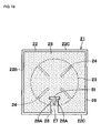
- the coupling electrodes 27 are surrounded by open portions (cutout portions) 28, which are arranged at end portions of the back-surface electrode 25 and each of which has a U-shape, so as to have a band-like shape (tongue-like shape) having a predetermined width W3.
- the coupling electrodes 27 extend in the radial direction of the substantially circular electrode 23 from the center of the back-surface electrode 25 to the end portion.
- a tip of each of the coupling electrodes 27 is surrounded by a corresponding one of the open portions 28 (cutout portions), which are arranged at the end portions of the back-surface electrode 25 and each of which has a U-shape, so as to be an open end.
- Base ends of the coupling electrodes 27 are connected to the back-surface electrode 25 and serve as short-circuit points S1.
- the tips (open ends) of the coupling electrodes 27 are connected to the signal lines 11 of the external substrate 10 using the bumps 15.
- Each of the short-circuit points S1 is arranged in the vicinity of a position having a large magnitude of magnetic field of the TM010-mode resonator 21, that is, a position where each of the short-circuit points S1 is strongly coupled with the TM010-mode resonator 21. Therefore, the short-circuit points S1 are arranged around intermediate portions (intermediate portions in the radial direction) between the axis O and an outer circumference edge of the substantially circular electrode 23.
- Each of the open portions 28 has portions between which a corresponding one of the coupling electrodes 27 is interposed and each of the portions has a predetermined gap width ⁇ 3. The portions of the open portions 28 sandwich each of the short-circuit points S1 in the width direction of the open portions 28.
- the dielectric resonance apparatus has the configuration described above, and an operation thereof will now be described.
- the high-frequency signals are supplied to the signal lines 11 of the external substrate 10, the high-frequency signals are supplied through the coupling electrodes 27 of the TM010-mode resonator 1 from the signal lines 11 and magnetic fields, each of which rotates within a YZ plane around a corresponding one of the coupling electrodes 27 as a center, are generated.
- a bandpass resonator is formed between the two coupling electrodes 27.
- a bandpass characteristic of the dielectric resonance apparatus according to this embodiment is analyzed by an electro-magnetic field simulation.
- Fig. 16 shows a result of the analysis.
- the dielectric substrate 22 has a length L1 of 1.94 mm, a thickness T1 of 0.30 mm, and a relative dielectric constant ⁇ r1 of 26.
- the substantially circular electrode 23 has a diameter D of 1.56 mm, and each of the cutout portions 24 has a groove width ⁇ p of 0.04 mm, and a groove length Lp of 0.35 mm.
- each of the coupling electrodes 27 has a width W1 of 0.15 mm
- each of the portions of each of the open portions 28, the portions sandwiching the corresponding short-circuit point S1 has a gap width ⁇ 3 of 0.075 mm
- the frame portion 8 has a width ⁇ 0 of 0.05 mm.
- the external substrate 10 has a thickness T0 of 0.20 mm, a relative dielectric constant ⁇ r0 of 10, and a characteristic impedance Z0 of 50 ⁇ .
- Each of the bumps 15 has a diameter ⁇ of 0.09 mm and a height h of 0.04 mm.
- a bandpass amount of the TM010-mode resonator 21 is large around a frequency band centered at 38 GHz, which is a resonant frequency whereas a bandpass amount of the TM010-mode resonator 1 is small in other frequency bands. Accordingly, a reaction resonator, in which a bandpass amount thereof is large around the resonant frequency band of the TM010-mode resonator 21, may be configured utilizing the dielectric resonance apparatus according to this embodiment.
- the coupling electrodes 27 having the short-circuit points S1 sandwiched by the open portions 28 arranged on the substantially circular electrode 23 serve as magnetic-field coupling portions, and the ends (tips) of the coupling electrodes 27 are connected to the signal lines 11 of the external substrate 10.
- the TM010-mode resonator 21 is connected in series to circuits arranged on a surface of the external substrate 10 on which the signal lines 11 are arranged. With this configuration, the TM010-mode resonator 21 including the two coupling electrodes 27 functions as a bandpass resonator, and accordingly, is configured as a bandpass resonator.
- the TM010-mode resonator 21 allows a high-frequency signal supplied to one of the coupling electrodes 27 from the signal lines 11 of the external substrate 10 to pass at the resonant frequency of the TM010-mode resonator 21 and reflects the high-frequency signal at other frequencies.
- the tips of the coupling electrodes 27 are surrounded by the U-shaped open portions 28 and connected to the signal lines 11 of the external substrate 10, and the base ends of the coupling electrodes 27 are connected to the back-surface electrode 25 and serve as the short-circuit points S1. Accordingly, the tips of the coupling electrodes 27, which are open ends, allow high-frequency signals to be supplied, and magnetic fields having large magnitudes are generated around the base ends of the coupling electrodes 27 serving as the short-circuit points S1 so that the coupling electrodes 27 and the TM010-mode resonator 21 are magnetically coupled with each other.
- the short-circuit points S1 included in the coupling electrodes 27 are sandwiched by the portions of the open portions 28 in the width direction, the magnetic fields H0 generated around the short-circuit points S1 in accordance with the width ⁇ 3 of portions of the open portions 28 located in the vicinity of the short-circuit points S1 change, and an amount of coupling between the coupling electrodes 27 and the TM010-mode resonator 21 changes.
- the gap width ⁇ 3 included in each of the open portions 28 is set to various values and a bandpass characteristic thereof is analyzed using a electro-magnetic field simulation similarly to Fig. 16.
- Fig. 17 shows a result of the analysis.
- an axis of abscissa represents a normalized frequency normalized by a resonant frequency.
- the magnetic field generated around the short-circuit points S1 is expanded and therefore an amount of coupling is increased by setting a value of the gap width ⁇ 3 included in each of the open portions 28 larger, whereas the magnetic field generated around the short-circuit points S1 is reduced and therefore an amount of coupling is reduced by setting the value of the gap width ⁇ 3 included in each of the open portions 28 smaller. Accordingly, the amount of coupling between the coupling electrodes 27 and the TM010-mode resonator 21 may be controlled to a desired value. A degree of freedom of design is enhanced.
- the gap widths ⁇ 3 included in the open portions 28 are uniform in all of the coupling electrodes 27.
- the present invention is not limited to this, and as a third modification shown in Fig. 18, the gap width of the open portions 28 may be designed so as to be large only around the short-circuit points S1, and therefore, large-width portions 28A may be designed at tips of the open portions 28. In this case, an amount of coupling is set in accordance with the gap width of each of the large-width portions.
- the amount of coupling between the coupling electrodes 27 and the TM010-mode resonator 21 is set to a desired amount in accordance with the gap width ⁇ 3 included in each of the open portions 28.
- the amount of coupling between the coupling electrodes 27 and the TM010-mode resonator 21 may be set to a desired amount in accordance with a distance between a portion in which a magnitude of the magnetic field of the TM010-mode resonator 21 is large (for example, an intermediate portion between the axis O of the substantially circular electrode 23 and the outer circumference edge) and the short-circuit points S1 of the coupling electrodes 27.
- the amount of coupling is increased by changing the position of the short-circuit points S1 so as to be close to the position where the magnitude of the magnetic field generated in the TM010-mode resonator 21 is large, whereas the amount of coupling is reduced by changing the position of the short-circuit points S1 so as to be far away from the position where a magnitude of the magnetic field generated in the TM010-mode resonator 21 is large.
- the amount of coupling with the TM010-mode resonator may be controlled to be a desired amount in accordance with the position of the short-circuit points S1. Hence, a degree of freedom of design is enhanced.
- the open portions 28 are configured as cutout portions extending from end portions toward the center of the back-surface electrode 25.
- the open portions 28 are not necessarily arranged in the end portions of the back-surface electrode 25, and open portions 28' may be arranged in positions nearer to the center of the back-surface electrode 25 as shown in a fourth modification illustrated in Fig. 19, to thereby form coupling electrodes 27', and therefore, the open portions 28' may be surrounded by the back-surface electrode 25.
- the coupling electrodes 27, each of which has a base end which serves as one of the short-circuit points S1 and which is connected to the back-surface electrode 25 and the tip which is an open end are constituted.
- the present invention is not limited to this.
- an open portion 28" having a rectangular frame shape may be arranged on the back-surface electrode 25, and therefore, a coupling electrode 27" which has both ends as open ends in the longitudinal direction and which has a virtual short-circuit point S1 in an intermediate portion thereof in the longitudinal direction may be constituted.
- a distance L between the short-circuit point S1 and the back-surface electrode 25 in the longitudinal direction is set to a value of approximately ⁇ g/4 (L ⁇ ⁇ g/4) with respect to a wavelength ⁇ g of a resonant frequency of the dielectric substrate 22.
- the back-surface electrode 25 is arranged to have a rectangular shape so as to entirely cover the back surface 22B of the dielectric substrate 22.
- the present invention is not limited to this, and the back-surface electrode 25' may be arranged, as a sixth modification shown in Fig. 21, so as to have a circular shape, an oval shape, and any other shape.
- the two coupling electrodes 27 are arranged on the back surface 22B of the dielectric substrate 22, only one coupling electrode 27 may be arranged. As a seventh modification shown in Fig. 22, three or more coupling electrodes 27 may be arranged.
- the cutout portions 24 are arranged on the substantially circular electrode 23 for controlling a resonant frequency for other resonance modes, the cutout portions may be omitted.
- the shape of the substantially circular electrode 23 is not limited to a circular shape, and may be an oval shape.
- two back-surface electrodes are arranged on either side of the coupling line serving as a magnetic-field coupling section and are arranged on a back surface of the dielectric substrate of the TM010-mode resonator. Furthermore, one of the back-surface electrodes has a coupling electrode which has a short-circuit point surrounded by an opening portion and which serves as another magnetic-field coupling section, and the oscillation apparatus is configured using a TM010-mode resonator.
- An oscillation circuit substrate 31 serving as an external substrate is made of an dielectric material.
- An oscillation circuit unit 32 and a frequency control circuit unit 40, which will be described later, are arranged on the oscillation circuit substrate 31 serving as an external substrate, and furthermore, a TM010-mode resonator 43 is implemented on a surface of the oscillation circuit substrate 31.
- the oscillation circuit unit 32 is arranged on the surface of an oscillation circuit substrate 31.
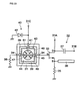
- the oscillation circuit unit 32 includes a field-effect transistor 33 (hereinafter referred to as FET 33) and first and second micro-strip lines 34.
- FET 33 field-effect transistor 33
- the oscillation circuit unit 32 receives a power-supply voltage through a power-supply terminal 31A, oscillates signals having a predetermined oscillation frequency set by the TM010-mode resonator 43, which will be described hereinafter, and outputs the signals through an output terminal 31B.
- a gate terminal G of the FET 33 is connected to a base end of the first micro-strip line 34.
- a source terminal S of the FET 33 is connected to a bias resistor 35 and a stub 36.
- a drain terminal D of the FET 33 is connected to the power-supply terminal 31A and also connected to the output terminal 31B through a coupled line 37 used for interrupting a direct current.
- the micro-strip lines 34 serve as signal lines and the first and second micro-strip lines 34 are arranged with the TM010-mode resonator 43 interposed therebetween.
- the first and second micro-strip lines 34 are arranged in positions except for positions facing a coupling line 47 of the TM010-mode resonator 43, and are linearly arranged.
- the first and second micro-strip lines 34 are connected to each other through the coupling line 47, and a terminal resistor 38 is connected to an end of the second micro-strip line 34.
- the two ground electrodes 39 are arranged on either side in a width direction of the micro-strip lines 34.
- the two ground electrodes 39 are arranged either side in the width direction of a portion of the TM010-mode resonator 43 facing the coupling line 47, and face two corresponding back-surface electrodes 49.
- the two ground electrodes 39 are connected to ground electrodes (not shown) arranged on a back surface of the oscillation circuit substrate 31 through via holes, for example.
- the frequency control circuit unit 40 is arranged on the surface of the oscillation circuit substrate 31.
- the frequency control circuit unit 40 mainly includes a micro-strip line 41 serving as a signal line and a variable capacitor diode 42 (varactor diode) serving as a modulation element.
- the micro-strip line 41 is connected to a coupling electrode 51 at one end thereof and connected to the variable capacitor diode 42 at the other end thereof.
- the variable capacitor diode 42 is connected to the micro-strip line 41 at the cathode terminal thereof and connected to the ground at the anode terminal thereof.
- the frequency control circuit unit 40 controls oscillation frequency (resonant frequency) by changing a capacitance in the variable capacitor diode 42 in accordance with a control voltage applied to a control-input terminal 31C.
- the TM010-mode resonator 43 is connected to the oscillation circuit unit 32 and the frequency control circuit unit 40.
- the TM010-mode resonator 43 includes a dielectric substrate 44, a substantially circular electrode 45, and back-surface electrodes 49, and is stacked on the surface of the oscillation circuit substrate 31.
- the dielectric substrate 44 has a substantially square plate shape.
- the substantially circular electrode 45 is arranged on a surface 44A of the dielectric substrate 44 so as to be located at the center of the dielectric substrate 44.
- the substantially circular electrode 45 is made of a dielectric thin film and has a diameter corresponding to a value obtained in accordance with a resonant frequency in the dielectric substrate 44.
- the substantially circular electrode 45 has four cutout portions 46 which are radially arranged.
- the coupling line 47 serves as a first magnetic-field coupling section. Substantially as with the case of the coupling line 5 according to the first embodiment, the coupling line 47 extends through a portion which is located on a back surface 44B of the dielectric substrate 44 and which faces the substantially circular electrode 45 toward an end portion of the dielectric substrate 44 (an end face 44C). Furthermore, the coupling line 47 linearly extends along the diameter of the substantially circular electrode 45 through an axis O of the substantially circular electrode 45.
- the coupling line 47 has connection portions 48 at both ends thereof used for connecting the micro-strip lines 34 of the oscillation circuit unit 32.
- the back-surface electrodes 49 are arranged on the back surface 44B of the dielectric substrate 44 and are arranged either side of the coupling line 47 in the width direction.
- the two back-surface electrodes 49 cover the entire back surface 44B of the dielectric substrate 44, face the substantially circular electrode 45 with the dielectric substrate 44 interposed therebetween, and are connected to the ground electrodes 39 of the oscillation circuit unit 32.
- a gap 50 having a predetermined width is formed between the coupling line 47 and the back-surface electrodes 49.
- the coupling electrode 51 serves as a second magnetic-field coupling section. As with the coupling electrodes 27 according to the second embodiment, the coupling electrode 51 is arranged so as to face the substantially circular electrode 45 and arranged on one of the back-surface electrodes 49 in the width direction of the coupling line 47.
- the coupling electrode 51 is surrounded by a U-shaped open portion 52 (cutout portion) which is formed at an edge of the back-surface electrodes 49 and which has a band-like shape (tongue-like shape).
- the coupling electrode 51 extends in the radial direction of the substantially circular electrode 45 from the center toward the edge of the back-surface electrodes 49.
- a tip of the coupling electrode 51 is an open end which is surrounded by the U-shaped open portion 52 whereas a base end of the coupling electrode 51 serves as a short-circuit point S1 connected to the back-surface electrodes 49.
- the short-circuit point S1 is sandwiched between portions of the open portion 52 in the width direction.
- the short-circuit point S1 is arranged in the vicinity of a portion of the TM010-mode resonator 43 where a magnitude of a magnetic-field is large, that is, a portion where the short-circuit point S1 is strongly coupled with the TM010-mode resonator 43.
- connection portions 48 of the coupling line 47 of the TM010-mode resonator 43 are connected to the micro-strip lines 34 arranged on the oscillation circuit unit 32 using bumps 53, and the back-surface electrodes 49 are connected to the ground electrodes 39 arranged on the oscillation circuit unit 32 using the bumps 53.
- the coupling electrode 51 of the TM010-mode resonator 43 is connected to the micro-strip line 41 of the frequency control circuit unit 40 using the bumps 53.
- the oscillation apparatus has the configuration described above, and an operation thereof will now be described.
- a driving voltage is applied to the power-supply terminal 31A, a signal based on a resonant frequency of the TM010-mode resonator 43 is supplied to the gate terminal G of the FET 33. Since the oscillation circuit unit 32 and the TM010-mode resonator 43 constitute a reaction oscillation circuit, the FET 33 amplifies the signal supplied on the basis of the resonant frequency of the TM010-mode resonator 43 and outputs the amplified signal through the output terminal 31B.
- the frequency control circuit unit 40 including the variable capacitor diode 42 is connected to the TM010-mode resonator 43, a resonant frequency of the TM010-mode resonator 43 is variably set in accordance with a value of a control voltage to be applied to the control-input terminal 31C. Therefore, the entire oscillation apparatus functions as a voltage-controlled oscillator (VCO).
- VCO voltage-controlled oscillator
- the coupling electrode 51 is arranged on one of the back-surface electrodes 49 which are arranged on either side of the coupling line 47 in the width direction. Accordingly, as with the first embodiment, the TM010-mode resonator 43 serves as a reaction resonator using the coupling line 47.
- the coupling electrode 51 since the coupling electrode 51 is connected to the frequency control circuit unit 40, the resonant frequency of the TM010-mode resonator 43 may be externally controlled. Consequently, a voltage-controlled oscillator is provided employing the TM010-mode resonator 43.
- the coupling line 47 and the coupling electrode 51 are arranged on the dielectric substrate 44 of the TM010-mode resonator 43, variation of an amount of coupling between the TM010-mode resonator 43 the coupling line 47 and an amount of coupling between the TM010-mode resonator 43 and the coupling electrode 51 is reduced. Accordingly, characteristics of individual oscillation apparatuses can be maintained substantially stable. Moreover, since the frequency control circuit unit 40 and the terminal resistor 38 may be removed from the dielectric substrate 44 of the TM010-mode resonator 43, the expensive dielectric substrate 44 which has a high dielectric constant and therefore is expensive may be miniaturized. Accordingly, since the variations of the characteristics are reduced, mass production of the oscillation apparatus is enhanced. Furthermore, since a compact dielectric substrate 44 is used, production cost is reduced.
- one coupling electrode 51 is arranged on one of the back-surface electrodes 49 which are arranged either side of the coupling line 47 in the width direction, and is connected to the frequency control circuit unit 40 including a variable element (the variable capacitor diode 42).
- the present invention is not limited to this.
- two coupling electrodes 51 may be arranged on both of the back-surface electrodes 49 which are arranged either side of the coupling line 47 in the width direction, one of the coupling electrodes 51 may be connected to the frequency control circuit unit 40 (the variable element), and the other coupling electrode 51 may be connected to a stub used for controlling frequencies.
- the TM010-mode resonator 43 according to the third embodiment is constituted by a combination of the TM010-mode resonator 1 according to the first embodiment and the TM010-mode resonator 21 according to the second embodiment.
- the present invention is not limited to this.
- a TM010-mode resonator employed for a oscillation apparatus may be configured by a combination of the TM010-mode resonators 1 and 21 according to the first to seventh modifications.
- a radar apparatus serving as a transmission/reception apparatus is configured using an oscillation apparatus including the dielectric resonance apparatus according to the invention.
- a radar apparatus 61 includes an oscillation apparatus 62, a coupler 64, a mixer 67, and a signal processing circuit 69, which will be described later, and serves as a millimeter-wave radar module.
- the oscillation apparatus 62 is constituted by a VCO employing the dielectric resonance apparatus according to the invention, and is connected to an antenna 66 through an isolator 63, the coupler 64, and a circulator 65. With this configuration, an high-frequency signal output from the oscillation apparatus 62 is externally transmitted through the antenna 66.
- the antenna 66 is connected to the mixer 67 through the circulator 65, and an output terminal of the mixer 67 is connected to the signal processing circuit 69 through a low-noise amplifier 68 (hereinafter referred to as an LNA 68).
- LNA 68 low-noise amplifier
- the radar apparatus 61 has the configuration as described above, and an operation thereof will now be described.
- a high-frequency signal output from the oscillation apparatus 62 is supplied to the antenna 66 through the isolator 63, the coupler 64, and the circulator 65.
- the antenna 66 emits a millimeter-wave signal as a sharp beam thereby to externally transmit the signal.
- the antenna 66 leads a reception signal obtained on the basis of the reflection to the mixer 67 through the circulator 65.
- the mixer 67 since the reception signal is input to the mixer 67, and in addition, a local signal, which is a part of a transmission signal from the coupler 64, is input from the coupler 64, the mixer 67 outputs a beat signal, which is an oscillation frequency signal obtained from a difference between the reception signal and the local signal, as an intermediate frequency signal.
- the intermediate frequency signal is amplified by the LNA 68 and supplied to the signal processing circuit 69.
- the signal processing circuit 69 performs digital-data column conversion and further performs FFT (fast Fourier transformation) processing on the intermediate frequency signal, whereby an oscillation frequency spectrum of the beat signal is obtained. Consequently, a distance and a relative velocity to the object are obtained from the relationship between a modulation signal supplied to the signal processing circuit 69 and the intermediate frequency signal.
- the oscillation apparatus 62 using the dielectric resonance apparatus according to the embodiment is used to configure a communication apparatus, variation of electric characteristics of individual radar apparatuses 61 can be reduced, and production cost may be reduced.
- the oscillation apparatus 62 using the dielectric resonance apparatus according to the present invention is employed for the radar apparatus 61
- the oscillation apparatus 62 may be employed for a communication device, for example.
Landscapes
- Control Of Motors That Do Not Use Commutators (AREA)
- Inductance-Capacitance Distribution Constants And Capacitance-Resistance Oscillators (AREA)
- Burglar Alarm Systems (AREA)
Abstract
Description
- The present invention relates to dielectric resonance apparatuses, which oscillate high-frequency electro-magnetic waves such as microwaves and millimeter waves, oscillation apparatuses using the dielectric resonance apparatuses, and transmission/reception apparatuses.
- In general, a known dielectric resonance apparatus includes a resonator having a circular electrode on a surface of a dielectric substrate and power-supply lines which are arranged on the dielectric substrate and which are arranged in the vicinity of ends of the resonator (refer to, for example, Patent Document 1).
- Furthermore, a known oscillation apparatus using a dielectric resonance apparatus includes an oscillator block which oscillates signals having predetermined oscillation frequencies and a dielectric resonator block constituted by a TM010-mode resonator used for setting the oscillation frequencies (refer to, for example, Patent Document 2). In such an oscillation apparatus, the oscillator block and the dielectric resonator block are separately configured using dielectric substrates. In addition, dielectric constants and the thicknesses of the dielectric substrates are suitably set for the oscillator block and the dielectric resonator block. Accordingly, a substrate having a low dielectric constant is used for the oscillator block, for example, whereby accuracy of dimension is relatively enhanced. On the other hand, a substrate having a high dielectric constant and a large thickness is used for the dielectric resonator block, whereby Q factor is enhanced. Furthermore, mass production of the oscillator apparatus is facilitated by using of the oscillator block and the resonator block in combination.
- A known waveguide dielectric resonator includes a substantially cuboid dielectric block (refer to, for example, Patent Document 3). Such a dielectric resonator includes an input/output electrode having a short-circuit point connected to a ground electrode so as to face a surface on which the dielectric block is implemented. Furthermore, the dielectric resonator is excited using the input/output electrode.
- Patent Document 1:
Japanese Unexamined Patent Application Publication No. 7-336106 - Patent Document 2:
Japanese Unexamined Patent Application Publication No. 11-234009 - Patent Document 3: International Publication No. WO
2002/078119 pamphlet - In the related art disclosed in
Patent Document 1, a distance between each of the power-supply lines and the ground is set larger than a distance between the resonator and the ground so that the power-supply lines and the resonator are strongly coupled with each other. In this case, since a large space is necessary in the thickness direction of the dielectric substrate, for example, so that a large distance between each of the power-supply lines and the ground surrounding the power-supply lines is ensured, the thickness of the dielectric resonance apparatus tends to be large. Furthermore, since the power-supply lines are arranged outside of the resonator, the area of the dielectric resonance apparatus also tends to be large. Accordingly, the size of the dielectric resonance apparatus is increased. - In the related art disclosed in
Patent Document 2, a frequency control circuit for controlling an oscillation frequency and a terminating resistor are arranged on the dielectric substrate of the dielectric resonator block. In this case, since the dielectric substrate used for the dielectric resonator block has a high dielectric constant, the cost tends to be increased, and furthermore, the area of the dielectric substrate tends to be increased. This leads to the problem that production cost of the oscillation apparatus is increased. - Moreover, in the related art disclosed in
Patent Document 3, since a waveguide dielectric resonator is used, electric characteristics of the resonator is determined in accordance with the length and width of the dielectric block. In this case, as processing methods of the dielectric block, a method for processing the dielectric block by baking after injection molding and a method for processing the dielectric block by cutting out by dicing after baking of a dielectric body have been proposed. However, such processing methods lead to large manufacturing error, and therefore, a desired accuracy of dimension is not obtained. Accordingly, it is necessary to enhance accuracies of the length and the width of the dielectric block by performing polishing after formation of the dielectric block, resulting in increased production cost. Furthermore, since an input/output electrode is arranged on the dielectric block which should be subjected to high-accuracy outer-shape processing, even if the dielectric block and the input/output electrode is slightly displaced with respect to each other, an amount of coupling between the dielectric resonator and the input/output electrode is changed. Consequently, variation of amounts of coupling between individual dielectric resonators and corresponding input/output electrodes is likely to be generated, and variation of electric characteristics of the resonators becomes large. - Accordingly, it is an object of the present invention to provide a dielectric resonance apparatus, an oscillation apparatus, and a transmission/reception apparatus, which are compact and have stable electric characteristics while production costs thereof are reduced.
- (1) In order to achieve the above-described object, a dielectric resonance apparatus according to the present invention includes a TM010-mode resonator including a dielectric substrate having electrodes arranged on a surface and a back surface thereof, the electrode arranged on the surface being a substantially circular electrode, an external substrate implemented on a plane of the back surface of the dielectric substrate so as to face the back surface of the dielectric substrate of the TM010-mode resonator, and signal lines which are arranged on the external substrate and which are connected to the TM010-mode resonator. In the dielectric resonance apparatus, a magnetic-field coupling section for magnetically coupling with the TM010-
mode resonator 1 by being connected to the signal lines is arranged on the back surface of the dielectric substrate.
According to the present invention, since the magnetic-field coupling section connected to the signal lines is arranged on the back surface of the dielectric substrate of the TM010-mode resonator, the magnetic field generated in the magnetic-field coupling section is made to coincide with a magnetic field generated in the TM010-mode resonator whereby the magnetic-field coupling section is magnetically coupled with the TM010-mode resonator. Accordingly, the TM010-mode resonator and the signal lines are connected with each other using the magnetic-field coupling section, and the TM010-mode resonator is excited by high-frequency signals supplied to the signal lines.
Since an electrode arranged on the back surface of the dielectric substrate serves as a magnetic-field coupling section, the electrode serving as a magnetic-field coupling section may be formed simultaneously (together) with the back-surface electrodes included in the TM010-mode resonator. Accordingly, a variation of an amount of coupling between the TM010-mode resonator and the magnetic-field coupling section may be reduced and electrical characteristics of the individual TM010-mode resonators may be kept constant. Furthermore, since the magnetic-field coupling section is arranged in a position facing the substantially circular electrode, the TM010-mode resonator may be made smaller when compared with a case where the magnetic-field coupling section is magnetically coupled with the TM010-mode resonator in a position facing the outside of the substantially circular electrode.
In the TM010-mode resonator, an electrical characteristic of the TM010-mode resonator is determined in accordance with the substantially circular electrode, the back-surface electrodes and the thickness T1 of the dielectric substrate, which constitute the TM010-mode resonator. Accordingly, since the magnetic-field coupling section and the back-surface electrodes are simultaneously formed, a stable coupling characteristic may be easily obtained. As a result, a fabrication cost may be reduced when compared with a case where a waveguide dielectric resonance apparatus for which high-accuracy processing is difficult is employed. Furthermore, since the magnetic-field coupling section has a stable coupling characteristic with respect to the TM010-mode resonator, a frequency control circuit and the like need not be arranged on the dielectric substrate of the TM010-mode resonator, but may be arranged on the external substrate. Since the frequency control circuit may be removed from the dielectric substrate, the TM010-mode resonator may be miniaturized. - (2) In this case, according to the present invention, the magnetic-field coupling section located on the back surface of the dielectric substrate may extend through a position facing the substantially circular electrode toward an end portion of the dielectric substrate, and may be constituted by a coupling line having opposite ends electrically connected to the signal lines arranged on the external substrate. Furthermore, the back-surface electrodes arranged on the back surface of the dielectric substrate may be located either side of the coupling line in a width direction and a gap may be provided so as to surround the coupling line.
In a case where the coupling line, which extends so as to pass through the position facing the substantially circular electrode, serves as a magnetic-field coupling section, and opposite ends thereof are connected to the signal lines arranged on the external substrate, the TM010-mode resonator is connected in parallel to a circuit arranged on the external substrate having the signal lines thereon. In this case, for example, a magnetic field having a direction the same as that of the circular magnetic field generated in the dielectric substrate of the TM010-mode resonator is generated around the coupling line by supplying a high-frequency signal having a resonant frequency to the coupling line. Therefore, since the coupling line and the TM010-mode resonator are magnetically coupled with each other, the high-frequency signal supplied from one of the opposite ends of the coupling line is reflected by the TM010-mode resonator. Consequently, a reaction resonator is constituted. - (3) In the present invention, the coupling line may pass through an axis of the substantially circular electrode.
According to the present invention, since the coupling line passes through the axis of the substantially circular electrode, a current loss due to existence of the coupling line may be reduced when compared with a case where the coupling line is arranged in any other position. That is, when the TM010-mode resonator is made to resonate, a resonant current is radially supplied toward the axis of the substantially circular electrode. If a configuration in which the coupling line is arranged so as to pass through a position other than the axis of the substantially circular electrode is employed, since the resonant current is interrupted by the gap arranged so as to surround both sides of the coupling line, a current loss of the TM010-mode resonator is increased. On the other hand, in the present invention, since the coupling line is arranged so as to pass through the axis of the substantially circular electrode, the resonant current is not interrupted by the gap surrounding both sides of the coupling line and a current loss due to the existence of the coupling line is reduced. - (4) In the present invention, the coupling line defines an amount of coupling with the TM010-mode resonator in accordance with a width of the coupling line.
According to the present invention, since an amount of coupling with the TM010-mode resonator is set in accordance with a width of the coupling line, the magnetic field generated around the coupling line is expanded and therefore an amount of coupling is increased by setting a value of the width of the coupling line larger, whereas the magnetic field generated around the coupling line is reduced and therefore an amount of coupling is reduced by setting the value of the width of the coupling line smaller. Accordingly, the amount of coupling between the coupling line and the TM010-mode resonator may be controlled to a desired value in accordance with the width of the coupling line. A degree of freedom of design is enhanced. - (5) the gap between the coupling line and each of the back-surface electrodes may define an amount of coupling with the TM010-mode resonator in accordance with a width of the gap.
According to the present invention, since an amount of coupling with the TM010-mode resonator is set in accordance with a width of the gap between the coupling line and each of the back-surface electrodes, the magnetic field generated around the coupling line is expanded and therefore an amount of coupling is increased by setting a value of the width of the gap larger, whereas the magnetic field generated around the coupling line is reduced and therefore an amount of coupling is reduced by setting the value of the width of the gap smaller. Accordingly, the amount of coupling between the coupling line and the TM010-mode resonator may be controlled to a desired value in accordance with the width of the gap. A degree of freedom of design is enhanced. - (6) In the present invention, signal lines and a ground electrode may be arranged on the external substrate in portions except for portions facing the coupling line of the TM010-mode resonator. The signal lines may be connected to end portions of the coupling line of the TM010-mode resonator using bumps. The ground electrode may be connected to a back-surface electrode of the TM010-mode resonator using the bumps.
According to the present invention, since signal lines and a ground electrode is arranged on the external substrate in portions except for portions facing the coupling line of the TM010-mode resonator, when the TM010-mode resonator is implemented on the external substrate, the ground electrodes on the external substrate and the like are not arranged around the coupling line. Accordingly, even if a variation in the heights of the bumps is generated when the coupling line and the back-surface electrodes on the TM010-mode resonator are connected to the signal lines and the ground electrodes on the external substrate, respectively, using the bumps, the magnetic field generated around the coupling line is not influenced by the ground electrodes of the external substrate. Consequently, even if the variation of the heights h of the bumps is generated, an amount of coupling between the TM010-mode resonator and the coupling line is kept constant, that is, stable coupling is achieved. - (7) Furthermore, in the present invention, the back-surface electrode arranged on the back surface of the dielectric substrate may be arranged so as to face the substantially circular electrode. Furthermore, the magnetic-field coupling section may be constituted by coupling electrodes having open portions and short-circuit points, each of the short-circuit points which is included in a corresponding one of the coupling electrodes being surrounded by the corresponding one of the open portions. Moreover, each of the coupling electrodes may be electrically connected to the signal lines arranged on the external substrate in a portion.
With this configuration, the TM010-mode resonator is connected in series to circuits arranged on a surface of theexternal substrate 10 on which the signal lines are arranged. Accordingly, a TM010-mode resonator including a coupling electrode functions as a reaction resonator, and a TM010-mode resonator including the two coupling electrodes functions as a bandpass resonator. Consequently, the TM010-mode resonator allows a high-frequency signal supplied to one of the coupling electrodes from a corresponding one of the signal lines of the external substrate to pass at the resonant frequency of the TM010-mode resonator and reflects the high-frequency signal at other frequencies. - (8) In this embodiment, U-shaped opening portions may be arranged on the back-surface electrode. Furthermore, the coupling electrodes may have tips surrounded by the corresponding U-shaped opening portions and connected to the corresponding signal lines arranged on the external substrate, and may have base ends which are connected to the back-surface electrode and serve as short-circuit points.
With this configuration, the tips of the coupling electrodes, which are open ends, allow high-frequency signals to be supplied, and magnetic fields having large magnitudes are generated around the base ends of the coupling electrodes serving as the short-circuit points so that the coupling electrodes and the TM010-mode resonator are magnetically coupled with each other. - (9) In the present invention, the coupling electrodes may define an amount of coupling with the TM010-mode resonator in accordance with a distance between a portion where a magnitude of a magnetic field of the TM010-mode resonator is large and the short-circuit points.
According to the present invention, since an amount of coupling with the TM010-mode resonator is set in accordance with a distance between a portion where a magnitude of a magnetic field of the TM010-mode resonator is large and the short-circuit points, the amount of coupling is increased by changing the position of the short-circuit points so as to be close to the position where the magnitude of the magnetic field generated in the TM010-mode resonator is large, whereas the amount of coupling is reduced by changing the position of the short-circuit points so as to be far away from the position where a magnitude of the magnetic field generated in the TM010-mode resonator is large. Accordingly, the amount of coupling with the TM010-mode resonator may be controlled to be a desired amount in accordance with the position of the short-circuit points. Hence, a degree of freedom of design is enhanced. - (10) In the present invention, the open portions may define an amount of coupling with the TM010-mode resonator in accordance with gap widths of portions located either side of the corresponding short-circuit points of the coupling electrodes.
According to the present invention, since the amount of coupling with TM010-mode resonator is set in accordance with a width of the gap included in the open portion, an amount of coupling is increased by setting a value of the gap width included in each of the open portions larger, whereas the magnetic field generated around the short-circuit points is reduced and therefore an amount of coupling is reduced by setting the value of the gap width included in each of the open portions smaller. Accordingly, the amount of coupling between the coupling electrodes and the TM010-mode resonator may be controlled to a desired value in accordance with the gap width included in each of the open portions. A degree of freedom of design is enhanced. - (11) In the present invention, another magnetic-field coupling section may be arranged on the back surface of the dielectric substrate of the TM010-mode resonator, and the other magnetic-field coupling section may have a short-circuit point which is surrounded by an open portion arranged on the back-surface electrode.
According to the present invention, since another magnetic-field coupling section is arranged on the back surface of the dielectric substrate of the TM010-mode resonator, and the other magnetic-field coupling section has a short-circuit point which is surrounded by an open portion arranged on the back-surface electrode, for example, in a state where a reaction resonator is constituted by the coupling line (a first magnetic-field coupling section), a reaction band of the reaction resonator may be controlled using a frequency control circuit unit by connecting the frequency control circuit unit to the coupling electrode (second magnetic-field coupling section) including the short-circuit point. Accordingly, a reaction voltage control oscillator is configured by connecting the oscillation circuit to the coupling line and by connecting the frequency control circuit unit to the coupling electrode including the short-circuit point. - (12) An oscillation apparatus and a transmission/reception apparatus may be configured utilizing the dielectric resonance apparatus according to the present invention.
- In this case, since the dielectric resonance apparatus is miniaturized and has a stable coupling characteristic, an oscillation apparatus and a transmission/reception apparatus using the dielectric resonance apparatus may be made compact while stable characteristics thereof are achieved.
-
- Fig. 1 is a perspective view showing a dielectric resonance apparatus according to a first embodiment of the present invention.
- Fig. 2 is an exploded perspective view illustrating a TM010-mode resonator and an external substrate shown in Fig. 1.
- Fig. 3 is a perspective view illustrating the TM010-mode resonator alone shown in Fig. 1.
- Fig. 4 is a sectional view of the TM010-mode resonator taking along a line IV-IV shown in Fig. 3 and viewed in a direction shown by arrows in Fig. 3.
- Fig. 5 is a plan view illustrating the TM010-mode resonator shown in Fig. 3.
- Fig. 6 is a bottom plan view illustrating the TM010-mode resonator shown in Fig. 3.
- Fig. 7 is a sectional view of the TM010-mode resonator taking along a line VII-VII shown in Fig. 1 and viewed in a direction shown by arrows in Fig. 1.
- Fig. 8 is an equivalent circuit illustrating the dielectric resonance apparatus shown in Fig. 1.
- Fig. 9 is a diagram illustrating a characteristic line which shows the relationship between a reflection amount and a frequency of the dielectric resonance apparatus according to the first embodiment.
- Fig. 10 is a diagram illustrating characteristic lines which show the relationships between a reflection amount and a normalized frequency of the dielectric resonance apparatus according to the first embodiment.
- Fig. 11 is a plan view illustrating a TM010-mode resonator according to a first modification.
- Fig. 12 is a bottom plan view illustrating a TM010-mode resonator according to a second modification.
- Fig. 13 is an exploded perspective view illustrating a TM010-mode resonator and an external substrate of a dielectric resonance apparatus according to a second embodiment.
- Fig. 14 is a plan view illustrating the TM010-mode resonator shown in Fig. 13.
- Fig. 15 is a bottom plan view illustrating the TM010-mode resonator shown in Fig. 13.
- Fig. 16 is a diagram illustrating a characteristic line which shows the relationship between a bandpass amount and a frequency of the dielectric resonance apparatus according to the second embodiment.
- Fig. 17 is a diagram illustrating characteristic lines which show the relationships between a bandpass amount and a normalized frequency of the dielectric resonance apparatus according to the second embodiment.
- Fig. 18 is a bottom plan view illustrating a TM010-mode resonator according to a third modification.
- Fig. 19 is a bottom plan view illustrating a TM010-mode resonator according to a fourth modification.
- Fig. 20 is a bottom plan view illustrating a TM010-mode resonator according to a fifth modification.
- Fig. 21 is a bottom plan view illustrating a TM010-mode resonator according to a sixth modification.
- Fig. 22 is a bottom plan view illustrating a TM010-mode resonator according to a seventh modification.
- Fig. 23 is a circuit diagram illustrating an oscillation apparatus according to a third embodiment.
- Fig. 24 is an exploded perspective view illustrating a TM010-mode resonator and an oscillation circuit substrate shown in Fig. 23.
- Fig. 25 is a plan view illustrating the TM010-mode resonator shown in Fig. 23.
- Fig. 26 is a bottom plan view illustrating the TM010-mode resonator shown in Fig. 23.
- Fig. 27 is a bottom plan view illustrating a TM010-mode resonator according to an eighth modification.
- Fig. 28 is a block diagram illustrating a radar apparatus according to a fourth embodiment.
- 1, 21, 43
- TM010-mode resonator
- 2, 22, 44
- dielectric substrate
- 3, 3', 23, 45
- substantially circular electrode
- 5, 47
- coupling line
- 7, 25, 25', 49
- back-surface electrode
- 9, 50
- gap
- 10
- external substrate
- 11
- signal line
- 13, 39
- ground electrode
- 15, 53
- bump
- 27, 27', 27", 51
- coupling electrode
- 28, 28', 28", 52
- open portion
- 31
- oscillation circuit substrate (external substrate)
- 32
- oscillation circuit unit
- 34, 41
- micro-strip lines (signal line)
- 40
- frequency control circuit unit
- 61
- radar apparatus (transmission/reception apparatus)
- 62
- oscillation apparatus
- A dielectric resonance apparatus, an oscillation apparatus, and a transmission/reception apparatus according to preferred embodiments of the present invention will be described in detail with reference to the accompanying drawings hereinafter.
- Referring to Figs. 1 to 8 which show a dielectric resonance apparatus according to a first embodiment, a TM010-
mode resonator 1 includes adielectric substrate 2, a substantiallycircular electrode 3, and a back-surface electrode 7, which will be described later. - The
dielectric substrate 2 has a plate shape (a chip shape) and is made of a dielectric material. An example of the dielectric material used for thedielectric substrate 2 is a ceramic material having a relative dielectric constant εr1 of approximately 26 (for example, εr = 26). Thedielectric substrate 2 is a substantially square plate having sides of length L1 in the X direction (vertical direction) and Y direction (horizontal direction) and having a thickness T1 in the Z direction (thickness direction). - The substantially
circular electrode 3 is disposed on asurface 2A of thedielectric substrate 2. The substantiallycircular electrode 3 is made of a dielectric thin film using a metal material, for example, and disposed in a center of thedielectric substrate 2. The substantiallycircular electrode 3 has a diameter of D which is defined in accordance with a resonance frequency of thedielectric substrate 2. - The substantially
circular electrode 3 has fourcutout portions 4 radially formed therein. The fourcutout portions 4 are arranged with equal intervals in a circumferential direction and each of the fourcutout portions 4 has a groove shape and extends along the radial direction and is used for setting a resonance frequency for other resonance modes (for example, a TM210 mode, and a TM310 mode). - A
coupling line 5 is included in a magnetic-field coupling section. Thecoupling line 5 is arranged on aback surface 2B of thedielectric substrate 2 so as to face the substantiallycircular electrode 3 and extends toward an end portion (anend face 2C) of thedielectric substrate 2. Thecoupling line 5 linearly extends through a center axis O of the substantiallycircular electrode 3 and extends along the diameter of the substantiallycircular electrode 3. Thecoupling line 5 has a predetermined width W1. Furthermore,connection portions 6 having a width W2 which is larger than the width W1 are arranged at opposite ends of thecoupling line 5 for facilitating the connection between thecoupling line 5 andsignal lines 11 which will be described later. Each of theconnection portions 6 has a width of W2 and a length of L2, which is of a value equal to a value of the width of W2, so as to have a substantially square shape, for example, and is connected to one of thesignal lines 11 disposed on anexternal substrate 10 which will be described later. - The two back-
surface electrodes 7 are disposed on theback surface 2B of thedielectric substrate 2 and disposed on either side of thecoupling line 5 in the width direction of thecoupling line 5. The two back-surface electrodes 7 cover theentire back surface 2B of thedielectric substrate 2 except for portions in the vicinity of the end face 2C of thedielectric substrate 2, and face the substantiallycircular electrode 3 with thedielectric substrate 2 interposed therebetween. Aframe portion 8 having a width of δ0 is formed between the back-surface electrode 7 and the end face 2C of thedielectric substrate 2. Thedielectric substrate 2 is exposed through theframe portion 8. -
Gap 9 is formed between the back-surface electrodes 7 and thecoupling line 5. Thegap 9 linearly extends along thecoupling line 5 and thegap 9 has a width of δ1. Thegap 9 functions as an insulator arranged between the back-surface electrodes 7 and thecoupling line 5. The width of thegap 9 is set to δ2 between the back-surface electrodes 7 and theconnection portions 6. - The TM010-
mode resonator 1 is implemented on theexternal substrate 10. Here, theexternal substrate 10 is made of a ceramic material or a resin material, for example, having a dielectric constant (for example, approximately εr = 10) comparatively lower than that of thedielectric substrate 2 which will be described later. As shown in Figs. 1 and 2, theexternal substrate 10 has a plate shape having a predetermined thickness T0. The TM010-mode resonator 1 is disposed on a surface of theexternal substrate 10 such that theback surface 2B of thedielectric substrate 2 faces the surface of theexternal substrate 10. Furthermore, thesignal lines 11 andground electrodes 13, which will be described later, are disposed on the surface of theexternal substrate 10 at any portions except for portions where the surface of theexternal substrate 10 faces thecoupling line 5 of the TM010-mode resonator 1. - The two
signal lines 11 are arranged on the surface of theexternal substrate 10. The signal lines 11 are arranged in positions different from positions where the TM010-mode resonator 1 faces thecoupling line 5, and linearly extend along an imaginary line extending from the ends of thecoupling line 5.Connection portions 12 are arranged at end portions of thesignal lines 11 so as to face theconnection portions 6 of thecoupling line 5. Theconnection portions 12 of thesignal lines 11 are superposed with theconnection portions 6 of thecoupling line 5 so that the TM010-mode resonator 1 and theexternal substrate 10 are connected with each other usingbumps 15 which will be described later. - The two
ground electrodes 13 are disposed on the surface of theexternal substrate 10 such that theground electrodes 13 are insulated from the signal lines 11. The twoground electrodes 13 are separately arranged in the width direction of the TM010-mode resonator 1 with a portion on theexternal substrate 10 facing thecoupling line 5 of the TM010-mode resonator 1 interposed therebetween. Theground electrodes 13 are connected to ground electrodes (not shown) formed on a back surface of theexternal substrate 10 through via holes 14. Theground electrodes 13 are connected to the back-surface electrodes 7 of the TM010-mode resonator 1 using thebumps 15. - The
bumps 15 are used to connect theexternal substrate 10 and the TM010-mode resonator 1 with each other. Each of thebumps 15 has a substantially cylindrical shape having a diameter of φ and a height of h, and is used for connecting theconnection portions 12 of thesignal lines 11 and theconnection portions 6 of thecoupling line 5, and connecting theground electrodes 13 and the back-surface electrodes 7. Thebumps 15 are projected from the surface of theexternal substrate 10 and support the TM010-mode resonator 1. - The dielectric resonance apparatus according to the embodiment has the configuration as described above, and operation thereof will now be described.
- When the TM010-
mode resonator 1 is made to resonate, as shown in Figs. 3 and 5, an electric field E is generated inside thedielectric substrate 2, that is, between the substantiallycircular electrode 3 and the back-surface electrodes 7 in the thickness direction of thedielectric substrate 2. Furthermore, a circular magnetic field H which concentrically rotates in an XY plane along the circumference of the substantiallycircular electrode 3 which is a concentric circle. A magnitude of the circular magnetic field H is small in the vicinity of an axis O of the substantiallycircular electrode 3 and in the vicinity of an outer circumference edge whereas a magnitude of the circular magnetic field H is large in an intermediate region (an intermediate region in a radial direction) between the axis P and the outer circumference edge. - When a high-frequency signal is supplied to the
signal lines 11 of theexternal substrate 10, the high-frequency signal is supplied from thesignal lines 11 to thecoupling line 5 of the TM010-mode resonator 1, and thereby generates a magnetic field H0 which rotates around thecoupling line 5 in a YZ plane. - When a frequency of the high-frequency signal is equal to a resonant frequency of the TM010-
mode resonator 1, a rotation direction of the magnetic field H0 rotated in accordance with the high-frequency signal is inverted every half wavelength. Accordingly, a point at which a magnitude of the circular magnetic field H of the TM010-mode resonator 1 is large and a point at which a magnitude of the magnetic field H0 generated due to the high-frequency signal coincide with each other, and vector components in the Y direction of the circular magnetic field H and the magnetic field H0 match. Consequently, since thecoupling line 5 is magnetically coupled with the signal lines 11, the TM010-mode resonator 1 is oscillated using thecoupling line 5. - Accordingly, the dielectric resonance apparatus according to the embodiment may be shown as an equivalent circuit illustrated in Fig. 8, and the
coupling line 5 functions as a strip line and is magnetically coupled with the TM010-mode resonator 1. Accordingly, a reaction resonator may be formed by setting one end of thecoupling line 5 as a terminal end. Here, a reaction resonator employing the dielectric resonance apparatus according to the embodiment is analyzed in terms of a reflection characteristic using an electro-magnetic field simulation. Fig. 9 shows the result of the analysis. - Note that the result of the analysis shown in Fig. 9 is obtained when the one end of the
coupling line 5 is set as a terminal end and a reflection amount with respect to a frequency characteristic of the TM010-mode resonator 1 viewed from the other end of thecoupling line 5 is calculated. In this electro-magnetic field simulation, thedielectric substrate 2 has a length L1 of 1.94 mm, a thickness T1 of 0.30 mm, and a relative dielectric constant εr1 of 26. The substantiallycircular electrode 3 has a diameter D of 1.56 mm, and each of thecutout portions 4 has a groove width δp of 0.04 mm, and a groove length Lp of 0.35 mm. Furthermore, thecoupling line 5 has a width W1 of 0.08 mm, each of theconnection portions 6 has a width W2 and a length L2 of 0.15 mm, a portion between thecoupling line 5 and the back-surface electrodes 7 in thegap 9 has a width δ0 of 0.030 mm, a portion between theconnection portions 6 and the back-surface electrodes 7 in thegap 9 has a width δ2 of 0.025 mm, and theframe portion 8 has a width δ0 of 0.05 mm. Theexternal substrate 10 has a thickness T0 of 0.20 mm, a relative dielectric constant εr0 of 10, and a characteristic impedance Z0 of 50 Ω. Each of thebumps 15 has a diameter φ of 0.09 mm and a height h of 0.04 mm. - Referring to Fig. 9, it can be seen that the amount of reflection of the TM010-
mode resonator 1 is large around a frequency band centered at 38 GHz, which is a resonant frequency whereas an amount of reflection of the TM010-mode resonator 1 is small in other frequency bands. Accordingly, a reaction resonator, in which an amount of reflection thereof is large around the resonant frequency band of the TM010-mode resonator 1, may be configured utilizing the dielectric resonance apparatus according to this embodiment. - According to this embodiment, since the
coupling line 5 connected to the signal lines 11 is arranged on theback surface 2B of thedielectric substrate 2 of the TM010-mode resonator 1, the magnetic field H0 generated in thecoupling line 5 is made to coincide with the circular magnetic field H generated in the TM010-mode resonator 1 whereby thecoupling line 5 is magnetically coupled with the TM010-mode resonator 1. Accordingly, the TM010-mode resonator 1 and thesignal lines 11 are connected with each other using thecoupling line 5, and the TM010-mode resonator 1 is excited by a high-frequency signal supplied to the signal lines 11. - Since the
coupling line 5 serving as a magnetic-field coupling section is arranged on theback surface 2B of thedielectric substrate 2, the TM010-mode resonator 1 may be easily connected to theexternal substrate 10 through thebumps 15. Furthermore, since thecoupling line 5 serving as a magnetic-field coupling section is arranged on theback surface 2B of thedielectric substrate 2 of the TM010-mode resonator 1, when compared with a case where a magnetic-field coupling section is arranged on theexternal substrate 10, a variation of an amount of coupling between the TM010-mode resonator 1 and thecoupling line 5 may be reduced, and a electrical characteristic of the TM010-mode resonator 1 may be kept substantially constant. Since thecoupling line 5 may be arranged in a position facing the substantiallycircular electrode 3, the TM010-mode resonator 1 may be made smaller when compared with a case where thecoupling line 5 is arranged in a position facing the outside of the substantiallycircular electrode 3. - Since the
coupling line 5 arranged on theback surface 2B of thedielectric substrate 2 serves as a magnetic-field coupling section, thecoupling line 5 may be formed simultaneously (together) with the back-surface electrodes 7 included in the TM010-mode resonator 1. Accordingly, a variation of an amount of coupling between the TM010-mode resonator 1 and thecoupling line 5 may be reduced and an electrical characteristic of the TM010-mode resonator 1 may be kept constant. Furthermore, since thecoupling line 5 is arranged in a position facing the substantiallycircular electrode 3, the TM010-mode resonator 1 may be made smaller when compared with a case where thecoupling line 5 is magnetically coupled with the TM010-mode resonator 1 in a position facing the outside of the substantiallycircular electrode 3. - In the TM010-
mode resonator 1, an electrical characteristic of the TM010-mode resonator 1 is determined in accordance with the substantiallycircular electrode 3 and the back-surface electrodes 7 and the thickness T1 of thedielectric substrate 2, which constitute the TM010-mode resonator 1. Accordingly, since thecoupling line 5 is simultaneously formed with the back-surface electrodes 7, a stable coupling characteristic may be easily obtained. As a result, a fabrication cost may be reduced when compared with a case where a waveguide dielectric resonance apparatus for which high-accuracy processing is difficult is employed. Furthermore, since thecoupling line 5 has a stable coupling characteristic with respect to the TM010-mode resonator 1, a frequency control circuit and the like need not be arranged on thedielectric substrate 2 of the TM010-mode resonator 1, but may be arranged on theexternal substrate 10. Since the frequency control circuit may be removed from thedielectric substrate 2, the TM010-mode resonator 1 may be miniaturized. - Note that, in this embodiment, the
coupling line 5, which is arranged at the position facing the substantiallycircular electrode 3, serves as a magnetic-field coupling section, and opposite ends thereof are connected to thesignal lines 11 arranged on theexternal substrate 10. Therefore, in this configuration, the TM010-mode resonator 1 is connected in parallel to a circuit arranged on theexternal substrate 10 having the signal lines 11 thereon. In this case, for example, the magnetic field H0 having a direction the same as that of the circular magnetic field H generated in thedielectric substrate 2 of the TM010-mode resonator 1 is generated around thecoupling line 5 by supplying a high-frequency signal having a frequency serving as a resonant frequency to thecoupling line 5. Therefore, since thecoupling line 5 and the TM010-mode resonator 1 are magnetically coupled with each other, the high-frequency signal supplied from one of the opposite ends of thecoupling line 5 is reflected by the TM010-mode resonator 1. Consequently, a reaction resonator is constituted and a degree of freedom of design of an oscillation apparatus, for example, is enhanced. - Since the
coupling line 5 passes through the axis O of the substantiallycircular electrode 3, a current loss due to existence of thecoupling line 5 may be reduced when compared with a case where thecoupling line 5 is arranged in any other position. That is, when the TM010-mode resonator 1 is made to resonate, as shown in Fig. 6, a resonant current I is radially supplied toward the axis O of the substantiallycircular electrode 3. If a configuration in which thecoupling line 5 is arranged so as to pass through a position other than the axis O of the substantiallycircular electrode 3 is employed, since the resonant current I is interrupted by thegap 9 arranged so as to surround both sides of thecoupling line 5, a current loss of the TM010-mode resonator 1 is increased. On the other hand, in this embodiment, since thecoupling line 5 is arranged so as to pass through the axis O of the substantiallycircular electrode 3, the resonant current I is not interrupted by thegap 9 and a current loss due to the existence of thecoupling line 5 is reduced. - Since the
signal lines 11 and theground electrodes 13 are arranged in a region on theexternal substrate 10 except for a region on theexternal substrate 10 where theexternal substrate 10 faces thecoupling line 5, when the TM010-mode resonator 1 is implemented on theexternal substrate 10, theground electrodes 13 on theexternal substrate 10 and the like are not arranged around thecoupling line 5. Accordingly, even if a variation in the height h of thebumps 15 is generated when thecoupling line 5 and the back-surface electrodes 7 on the TM010-mode resonator 1 are connected to thesignal lines 11 and theground electrodes 13 on theexternal substrate 10, respectively, using thebumps 15, the magnetic field H0 generated around thecoupling line 5 is not influenced by theground electrodes 13 of theexternal substrate 10. Consequently, even if the variation of the heights h of thebumps 15 is generated, an amount of coupling between the TM010-mode resonator 1 and the coupling line is kept constant, that is, stable coupling is achieved. - In this embodiment, since the
gap 9 is arranged in the width direction of thecoupling line 5 so as to surround thecoupling line 5, the magnetic field H0 generated around thecoupling line 5 in accordance with the width δ1 of thegap 9 is changed, and the amount of coupling between thecoupling line 5 and the TM010-mode resonator 1 is changed. Here, the width δ1 of thegap 9 is set to various values, and a reaction resonator employing the dielectric resonance apparatus according to the embodiment is analyzed in terms of a reflection characteristic using a electro-magnetic field simulation similarly to Fig. 9. Fig. 10 shows the result of the analysis. - In this electro-magnetic field simulation, the various values of the width δ1 of the
gap 9 include 0.02 mm, 0.03 mm, and 0.04 mm. Parameters other than the width δ1 of thegap 9 are set to the same values as those where the result shown in Fig. 9 is obtained. The axis of abscissa in Fig. 10 illustrates a normalized frequency, which is normalized using a resonant frequency. - As is apparent from the result of the analysis shown in Fig. 10, when the width δ1 of the
gap 9 is small, an amount of reflection of the TM010-mode resonator 1 is small whereas when the width δ1 of thegap 9 becomes large, the amount of reflection of the TM010-mode resonator 1 is large. This is because as the width δ1 of thegap 9 is larger, the magnetic field H0 generated in thedielectric substrate 2 is expanded in the Y direction, and a Q factor (Qe) for the coupling with the TM010-mode resonator 1 becomes smaller to enhance the coupling. - As described above, the magnetic field H0 generated around the
coupling line 5 is expanded and therefore an amount of coupling is increased by setting a value of the width δ1 of thegap 9 larger, whereas the magnetic field H0 generated around thecoupling line 5 is reduced and therefore an amount of coupling is reduced by setting the value of the width δ1 of thegap 9 smaller. Accordingly, the amount of coupling between thecoupling line 5 and the TM010-mode resonator 1 may be controlled to a desired value. A degree of freedom of design is enhanced. - In the first embodiment, the amount of coupling between the
coupling line 5 and the TM010-mode resonator 1 is set to a desired value in accordance with the width δ1 of thegap 9. However, the amount of coupling between thecoupling line 5 and the TM010-mode resonator 1 may be set to the desired value in accordance with the width W1 of thecoupling line 5. In this case, the magnetic field generated around thecoupling line 5 is expanded and therefore an amount of coupling is increased by setting a value of the width W1 of thecoupling line 5 larger, whereas the magnetic field generated around thecoupling line 5 is reduced and therefore an amount of coupling is reduced by setting the value of the width W1 of thecoupling line 5 smaller. - In the first embodiment, the four
cutout portions 4 are arranged on the substantiallycircular electrode 3 for controlling a resonant frequency for other resonance modes. However, as illustrated as a first modification in Fig. 11, a substantially circular electrode 3' without cutout portions may be employed. A shape of the substantiallycircular electrode 3 is not limited to the circular shape but may be an oval shape. - In the first embodiment, the
connection portions 6, each of which has a large width, are arranged on either side of thecoupling line 5. However, as shown in a second modification shown in Fig. 12, the connection portions may be eliminated and thecoupling line 5 may be extended. - In the first embodiment, each of the two back-
surface electrodes 7 has a square shape and the back-surface electrodes 7 cover theentire back surface 2B of thedielectric substrate 2. However, the present invention is not limited to this and each of the back-surface electrodes may have a circular shape, or an oval shape, for example. - In the first embodiment, the
coupling line 5 of the TM010-mode resonator 1 and thesignal lines 11 of theexternal substrate 10 are directly connected. However, the present invention is not limited to this. Thecoupling line 5 and thesignal lines 11 may be connected through a matching circuit. In this case, the matching circuit may be arranged on one of thedielectric substrate 2 and theexternal substrate 10, or may be arranged on both of thedielectric substrate 2 and theexternal substrate 10. - Figs. 13 to 15 shows a dielectric resonance apparatus according to a second embodiment of the present invention. According to the second embodiment, a back-surface electrode which covers a substantially circular electrode is arranged on a back surface of a dielectric substrate of a TM010-mode resonator, coupling electrodes, which have short-circuit points each arranged between ends of an open portion arranged on the back-surface electrode, serve as magnetic-field coupling sections, and each of the coupling electrodes and a corresponding one of signal lines on an external substrate are connected at one point. In this embodiment, the same reference numerals are used for components having the same functions as those described in the first embodiment, and the descriptions thereof are omitted.
- A TM010-
mode resonator 21 includes adielectric substrate 22, a substantiallycircular electrode 23, and a back-surface electrode 25, which are similar to the dielectric substrate of the TM010-mode resonator 1 described in the first embodiment and which will be described later. - The
dielectric substrate 22 has a plate-like shape and is made of a dielectric material having a relative dielectric constant εr1. Thedielectric substrate 22 is a substantially square plate having sides of length L1 in the X direction (vertical direction) and Y direction (horizontal direction) and having a thickness T1 in the Z direction (thickness direction). - The substantially
circular electrode 23 is disposed on asurface 22A of thedielectric substrate 22. The substantiallycircular electrode 23 is made of a dielectric thin film, for example, and disposed in a center of thedielectric substrate 22. The substantiallycircular electrode 23 has a diameter D which is defined in accordance with a resonance frequency of thedielectric substrate 22. Fourcutout portions 24 are radially arranged in the substantiallycircular electrode 23 similarly to the substantiallycircular electrode 3 of the first embodiment. - The back-
surface electrode 25 is arranged on aback surface 22B of thedielectric substrate 22. The back-surface electrode 25 covers theentire back surface 22B of thedielectric substrate 22 except for portions in the vicinities of end faces 22C of thedielectric substrate 22, and faces the substantiallycircular electrode 23 with thedielectric substrate 22 interposed therebetween. Aframe portion 26 having a width of δ0 is formed between the back-surface electrode 25 and the end faces 22C of thedielectric substrate 22. Thedielectric substrate 22 is exposed through theframe portion 26. The back-surface electrode 25 is connected to theground electrodes 13 of theexternal substrate 10. - Two
coupling electrodes 27 serve as magnetic-field coupling sections. The twocoupling electrodes 27 are arranged on either side of the back-surface electrode 25 in the X direction so as to face the substantiallycircular electrode 23. Thecoupling electrodes 27 are surrounded by open portions (cutout portions) 28, which are arranged at end portions of the back-surface electrode 25 and each of which has a U-shape, so as to have a band-like shape (tongue-like shape) having a predetermined width W3. Thecoupling electrodes 27 extend in the radial direction of the substantiallycircular electrode 23 from the center of the back-surface electrode 25 to the end portion. A tip of each of thecoupling electrodes 27 is surrounded by a corresponding one of the open portions 28 (cutout portions), which are arranged at the end portions of the back-surface electrode 25 and each of which has a U-shape, so as to be an open end. Base ends of thecoupling electrodes 27 are connected to the back-surface electrode 25 and serve as short-circuit points S1. The tips (open ends) of thecoupling electrodes 27 are connected to thesignal lines 11 of theexternal substrate 10 using thebumps 15. - Each of the short-circuit points S1 is arranged in the vicinity of a position having a large magnitude of magnetic field of the TM010-
mode resonator 21, that is, a position where each of the short-circuit points S1 is strongly coupled with the TM010-mode resonator 21. Therefore, the short-circuit points S1 are arranged around intermediate portions (intermediate portions in the radial direction) between the axis O and an outer circumference edge of the substantiallycircular electrode 23. Each of theopen portions 28 has portions between which a corresponding one of thecoupling electrodes 27 is interposed and each of the portions has a predetermined gap width δ3. The portions of theopen portions 28 sandwich each of the short-circuit points S1 in the width direction of theopen portions 28. - The dielectric resonance apparatus according to this embodiment has the configuration described above, and an operation thereof will now be described.
- When high-frequency signals are supplied to the
signal lines 11 of theexternal substrate 10, the high-frequency signals are supplied through thecoupling electrodes 27 of the TM010-mode resonator 1 from thesignal lines 11 and magnetic fields, each of which rotates within a YZ plane around a corresponding one of thecoupling electrodes 27 as a center, are generated. - When frequencies of the high-frequency signals are the same as a resonance frequency of the TM010-
mode resonator 21, magnitudes of the magnetic fields become large at the short-circuit points S1 and become small in the vicinity of the outer circumference edge of the substantiallycircular electrode 23. Consequently, the position where the magnitude of the magnetic field of the TM010-mo resonator 1 itself is large and the position where the magnitude of the magnetic field of the TM010-mode resonator 1 is large due to the high-frequency signals coincide with each other, and the position where the magnitude of the magnetic field of the TM010-mode resonator 1 itself is small and the position where the magnitude of the magnetic field of the TM010-mode resonator 1 is small due to the high-frequency signal coincide with each other. Furthermore, vector components of the two magnetic fields coincide with each other around the short-circuit points S1. Consequently, since thecoupling line 5 is magnetically coupled with the signal lines 11, the TM010-mode resonator 21 is excited using thecoupling electrodes 27. - Accordingly, since the
coupling electrodes 27 are magnetically connected to the TM010-mode resonator 1, a bandpass resonator is formed between the twocoupling electrodes 27. Here, a bandpass characteristic of the dielectric resonance apparatus according to this embodiment is analyzed by an electro-magnetic field simulation. Fig. 16 shows a result of the analysis. - In the electro-magnetic field simulation, the
dielectric substrate 22 has a length L1 of 1.94 mm, a thickness T1 of 0.30 mm, and a relative dielectric constant εr1 of 26. The substantiallycircular electrode 23 has a diameter D of 1.56 mm, and each of thecutout portions 24 has a groove width δp of 0.04 mm, and a groove length Lp of 0.35 mm. Furthermore, each of thecoupling electrodes 27 has a width W1 of 0.15 mm, each of the portions of each of theopen portions 28, the portions sandwiching the corresponding short-circuit point S1, has a gap width δ3 of 0.075 mm, theframe portion 8 has a width δ0 of 0.05 mm. Theexternal substrate 10 has a thickness T0 of 0.20 mm, a relative dielectric constant εr0 of 10, and a characteristic impedance Z0 of 50 Ω. Each of thebumps 15 has a diameter φ of 0.09 mm and a height h of 0.04 mm. - Referring to Fig. 16, it can be seen that a bandpass amount of the TM010-
mode resonator 21 is large around a frequency band centered at 38 GHz, which is a resonant frequency whereas a bandpass amount of the TM010-mode resonator 1 is small in other frequency bands. Accordingly, a reaction resonator, in which a bandpass amount thereof is large around the resonant frequency band of the TM010-mode resonator 21, may be configured utilizing the dielectric resonance apparatus according to this embodiment. - Accordingly, in this embodiment, an operation effect similar to that of the first embodiment is obtained. Particularly, in this embodiment, the
coupling electrodes 27 having the short-circuit points S1 sandwiched by theopen portions 28 arranged on the substantiallycircular electrode 23 serve as magnetic-field coupling portions, and the ends (tips) of thecoupling electrodes 27 are connected to thesignal lines 11 of theexternal substrate 10. Accordingly, the TM010-mode resonator 21 is connected in series to circuits arranged on a surface of theexternal substrate 10 on which thesignal lines 11 are arranged. With this configuration, the TM010-mode resonator 21 including the twocoupling electrodes 27 functions as a bandpass resonator, and accordingly, is configured as a bandpass resonator. Consequently, the TM010-mode resonator 21 allows a high-frequency signal supplied to one of thecoupling electrodes 27 from thesignal lines 11 of theexternal substrate 10 to pass at the resonant frequency of the TM010-mode resonator 21 and reflects the high-frequency signal at other frequencies. - In this embodiment, the tips of the
coupling electrodes 27 are surrounded by the U-shapedopen portions 28 and connected to thesignal lines 11 of theexternal substrate 10, and the base ends of thecoupling electrodes 27 are connected to the back-surface electrode 25 and serve as the short-circuit points S1. Accordingly, the tips of thecoupling electrodes 27, which are open ends, allow high-frequency signals to be supplied, and magnetic fields having large magnitudes are generated around the base ends of thecoupling electrodes 27 serving as the short-circuit points S1 so that thecoupling electrodes 27 and the TM010-mode resonator 21 are magnetically coupled with each other. - In this embodiment, since the short-circuit points S1 included in the
coupling electrodes 27 are sandwiched by the portions of theopen portions 28 in the width direction, the magnetic fields H0 generated around the short-circuit points S1 in accordance with the width δ3 of portions of theopen portions 28 located in the vicinity of the short-circuit points S1 change, and an amount of coupling between thecoupling electrodes 27 and the TM010-mode resonator 21 changes. Here, in a bandpass resonator employing the dielectric resonance apparatus according to this embodiment, the gap width δ3 included in each of theopen portions 28 is set to various values and a bandpass characteristic thereof is analyzed using a electro-magnetic field simulation similarly to Fig. 16. Fig. 17 shows a result of the analysis. - Note that, in this electro-magnetic field simulation, a calculation is performed under conditions where the gap width δ3 included in each of the
open portions 28 is set to 0.075 mm, 0.10, and 0.125 mm. Parameters other than the gap width δ3 included in each of theopen portions 28 are set to the same values as obtained in the result of the analysis shown in Fig. 16. On Fig. 17, an axis of abscissa represents a normalized frequency normalized by a resonant frequency. - As can be seen from the result of analysis shown in Fig. 17, when the gap width δ3 included in each of the
open portions 28 is small, a bandpass amount of the TM010-mode resonator 21 is small, whereas when the gap width δ3 included in each of theopen portions 28 is large, a bandpass amount of the TM010-mode resonator 21 is large. This is because as the gap width δ3 included in each of theopen portions 28 becomes large, a magnetic field generated in thedielectric substrate 22 expands in the Y direction and Q factor (Qe) for the coupling with the TM010-mode resonator 21 becomes smaller to enhance the coupling. - As described above, the magnetic field generated around the short-circuit points S1 is expanded and therefore an amount of coupling is increased by setting a value of the gap width δ3 included in each of the
open portions 28 larger, whereas the magnetic field generated around the short-circuit points S1 is reduced and therefore an amount of coupling is reduced by setting the value of the gap width δ3 included in each of theopen portions 28 smaller. Accordingly, the amount of coupling between thecoupling electrodes 27 and the TM010-mode resonator 21 may be controlled to a desired value. A degree of freedom of design is enhanced. - In the second embodiment, the gap widths δ3 included in the
open portions 28 are uniform in all of thecoupling electrodes 27. However, the present invention is not limited to this, and as a third modification shown in Fig. 18, the gap width of theopen portions 28 may be designed so as to be large only around the short-circuit points S1, and therefore, large-width portions 28A may be designed at tips of theopen portions 28. In this case, an amount of coupling is set in accordance with the gap width of each of the large-width portions. - In the second embodiment, the amount of coupling between the
coupling electrodes 27 and the TM010-mode resonator 21 is set to a desired amount in accordance with the gap width δ3 included in each of theopen portions 28. However, the present invention is not limited to this. The amount of coupling between thecoupling electrodes 27 and the TM010-mode resonator 21 may be set to a desired amount in accordance with a distance between a portion in which a magnitude of the magnetic field of the TM010-mode resonator 21 is large (for example, an intermediate portion between the axis O of the substantiallycircular electrode 23 and the outer circumference edge) and the short-circuit points S1 of thecoupling electrodes 27. In this case, the amount of coupling is increased by changing the position of the short-circuit points S1 so as to be close to the position where the magnitude of the magnetic field generated in the TM010-mode resonator 21 is large, whereas the amount of coupling is reduced by changing the position of the short-circuit points S1 so as to be far away from the position where a magnitude of the magnetic field generated in the TM010-mode resonator 21 is large. Accordingly, the amount of coupling with the TM010-mode resonator may be controlled to be a desired amount in accordance with the position of the short-circuit points S1. Hence, a degree of freedom of design is enhanced. - In the second embodiment, the
open portions 28 are configured as cutout portions extending from end portions toward the center of the back-surface electrode 25. However, theopen portions 28 are not necessarily arranged in the end portions of the back-surface electrode 25, and open portions 28' may be arranged in positions nearer to the center of the back-surface electrode 25 as shown in a fourth modification illustrated in Fig. 19, to thereby form coupling electrodes 27', and therefore, the open portions 28' may be surrounded by the back-surface electrode 25. - In the second embodiment, since the U-shaped
open portions 28 are arranged on the back-surface electrode 25, thecoupling electrodes 27, each of which has a base end which serves as one of the short-circuit points S1 and which is connected to the back-surface electrode 25 and the tip which is an open end, are constituted. However, the present invention is not limited to this. As a fifth modification shown in Fig. 20, anopen portion 28" having a rectangular frame shape may be arranged on the back-surface electrode 25, and therefore, acoupling electrode 27" which has both ends as open ends in the longitudinal direction and which has a virtual short-circuit point S1 in an intermediate portion thereof in the longitudinal direction may be constituted. In this case, a distance L between the short-circuit point S1 and the back-surface electrode 25 in the longitudinal direction is set to a value of approximately λg/4 (L ≈ λg/4) with respect to a wavelength λg of a resonant frequency of thedielectric substrate 22. - In the second embodiment, the back-
surface electrode 25 is arranged to have a rectangular shape so as to entirely cover theback surface 22B of thedielectric substrate 22. However, the present invention is not limited to this, and the back-surface electrode 25' may be arranged, as a sixth modification shown in Fig. 21, so as to have a circular shape, an oval shape, and any other shape. - In the second embodiment, although the two
coupling electrodes 27 are arranged on theback surface 22B of thedielectric substrate 22, only onecoupling electrode 27 may be arranged. As a seventh modification shown in Fig. 22, three ormore coupling electrodes 27 may be arranged. - In the second embodiment, although the
cutout portions 24 are arranged on the substantiallycircular electrode 23 for controlling a resonant frequency for other resonance modes, the cutout portions may be omitted. Furthermore, the shape of the substantiallycircular electrode 23 is not limited to a circular shape, and may be an oval shape. - Referring to Figs. 23 to 26, an oscillation apparatus according to a third embodiment of the present invention will now be described. In this embodiment, two back-surface electrodes are arranged on either side of the coupling line serving as a magnetic-field coupling section and are arranged on a back surface of the dielectric substrate of the TM010-mode resonator. Furthermore, one of the back-surface electrodes has a coupling electrode which has a short-circuit point surrounded by an opening portion and which serves as another magnetic-field coupling section, and the oscillation apparatus is configured using a TM010-mode resonator.
- An
oscillation circuit substrate 31 serving as an external substrate is made of an dielectric material. Anoscillation circuit unit 32 and a frequencycontrol circuit unit 40, which will be described later, are arranged on theoscillation circuit substrate 31 serving as an external substrate, and furthermore, a TM010-mode resonator 43 is implemented on a surface of theoscillation circuit substrate 31. - The
oscillation circuit unit 32 is arranged on the surface of anoscillation circuit substrate 31. Theoscillation circuit unit 32 includes a field-effect transistor 33 (hereinafter referred to as FET 33) and first and second micro-strip lines 34. Theoscillation circuit unit 32 receives a power-supply voltage through a power-supply terminal 31A, oscillates signals having a predetermined oscillation frequency set by the TM010-mode resonator 43, which will be described hereinafter, and outputs the signals through anoutput terminal 31B. - A gate terminal G of the
FET 33 is connected to a base end of the firstmicro-strip line 34. A source terminal S of theFET 33 is connected to abias resistor 35 and astub 36. A drain terminal D of theFET 33 is connected to the power-supply terminal 31A and also connected to theoutput terminal 31B through a coupledline 37 used for interrupting a direct current. - The micro-strip lines 34 serve as signal lines and the first and second
micro-strip lines 34 are arranged with the TM010-mode resonator 43 interposed therebetween. The first and secondmicro-strip lines 34 are arranged in positions except for positions facing acoupling line 47 of the TM010-mode resonator 43, and are linearly arranged. The first and secondmicro-strip lines 34 are connected to each other through thecoupling line 47, and aterminal resistor 38 is connected to an end of the secondmicro-strip line 34. - As with the case of the
ground electrodes 13 according to the first embodiment, the twoground electrodes 39 are arranged on either side in a width direction of the micro-strip lines 34. The twoground electrodes 39 are arranged either side in the width direction of a portion of the TM010-mode resonator 43 facing thecoupling line 47, and face two corresponding back-surface electrodes 49. The twoground electrodes 39 are connected to ground electrodes (not shown) arranged on a back surface of theoscillation circuit substrate 31 through via holes, for example. - The frequency
control circuit unit 40 is arranged on the surface of theoscillation circuit substrate 31. The frequencycontrol circuit unit 40 mainly includes amicro-strip line 41 serving as a signal line and a variable capacitor diode 42 (varactor diode) serving as a modulation element. Themicro-strip line 41 is connected to acoupling electrode 51 at one end thereof and connected to thevariable capacitor diode 42 at the other end thereof. Thevariable capacitor diode 42 is connected to themicro-strip line 41 at the cathode terminal thereof and connected to the ground at the anode terminal thereof. - The frequency
control circuit unit 40 controls oscillation frequency (resonant frequency) by changing a capacitance in thevariable capacitor diode 42 in accordance with a control voltage applied to a control-input terminal 31C. - The TM010-
mode resonator 43 is connected to theoscillation circuit unit 32 and the frequencycontrol circuit unit 40. The TM010-mode resonator 43 includes adielectric substrate 44, a substantiallycircular electrode 45, and back-surface electrodes 49, and is stacked on the surface of theoscillation circuit substrate 31. - The
dielectric substrate 44 has a substantially square plate shape. The substantiallycircular electrode 45 is arranged on asurface 44A of thedielectric substrate 44 so as to be located at the center of thedielectric substrate 44. The substantiallycircular electrode 45 is made of a dielectric thin film and has a diameter corresponding to a value obtained in accordance with a resonant frequency in thedielectric substrate 44. As with the case of the substantiallycircular electrode 3 according to the first embodiment, the substantiallycircular electrode 45 has fourcutout portions 46 which are radially arranged. - The
coupling line 47 serves as a first magnetic-field coupling section. Substantially as with the case of thecoupling line 5 according to the first embodiment, thecoupling line 47 extends through a portion which is located on aback surface 44B of thedielectric substrate 44 and which faces the substantiallycircular electrode 45 toward an end portion of the dielectric substrate 44 (anend face 44C). Furthermore, thecoupling line 47 linearly extends along the diameter of the substantiallycircular electrode 45 through an axis O of the substantiallycircular electrode 45. Thecoupling line 47 hasconnection portions 48 at both ends thereof used for connecting themicro-strip lines 34 of theoscillation circuit unit 32. - The back-
surface electrodes 49 are arranged on theback surface 44B of thedielectric substrate 44 and are arranged either side of thecoupling line 47 in the width direction. The two back-surface electrodes 49 cover theentire back surface 44B of thedielectric substrate 44, face the substantiallycircular electrode 45 with thedielectric substrate 44 interposed therebetween, and are connected to theground electrodes 39 of theoscillation circuit unit 32. Agap 50 having a predetermined width is formed between thecoupling line 47 and the back-surface electrodes 49. - The
coupling electrode 51 serves as a second magnetic-field coupling section. As with thecoupling electrodes 27 according to the second embodiment, thecoupling electrode 51 is arranged so as to face the substantiallycircular electrode 45 and arranged on one of the back-surface electrodes 49 in the width direction of thecoupling line 47. Thecoupling electrode 51 is surrounded by a U-shaped open portion 52 (cutout portion) which is formed at an edge of the back-surface electrodes 49 and which has a band-like shape (tongue-like shape). Thecoupling electrode 51 extends in the radial direction of the substantiallycircular electrode 45 from the center toward the edge of the back-surface electrodes 49. A tip of thecoupling electrode 51 is an open end which is surrounded by the U-shapedopen portion 52 whereas a base end of thecoupling electrode 51 serves as a short-circuit point S1 connected to the back-surface electrodes 49. The short-circuit point S1 is sandwiched between portions of theopen portion 52 in the width direction. The short-circuit point S1 is arranged in the vicinity of a portion of the TM010-mode resonator 43 where a magnitude of a magnetic-field is large, that is, a portion where the short-circuit point S1 is strongly coupled with the TM010-mode resonator 43. - The both ends (connection portions 48) of the
coupling line 47 of the TM010-mode resonator 43 are connected to themicro-strip lines 34 arranged on theoscillation circuit unit 32 usingbumps 53, and the back-surface electrodes 49 are connected to theground electrodes 39 arranged on theoscillation circuit unit 32 using thebumps 53. Thecoupling electrode 51 of the TM010-mode resonator 43 is connected to themicro-strip line 41 of the frequencycontrol circuit unit 40 using thebumps 53. - The oscillation apparatus according to this embodiment has the configuration described above, and an operation thereof will now be described.
- When a driving voltage is applied to the power-
supply terminal 31A, a signal based on a resonant frequency of the TM010-mode resonator 43 is supplied to the gate terminal G of theFET 33. Since theoscillation circuit unit 32 and the TM010-mode resonator 43 constitute a reaction oscillation circuit, theFET 33 amplifies the signal supplied on the basis of the resonant frequency of the TM010-mode resonator 43 and outputs the amplified signal through theoutput terminal 31B. - Since the frequency
control circuit unit 40 including thevariable capacitor diode 42 is connected to the TM010-mode resonator 43, a resonant frequency of the TM010-mode resonator 43 is variably set in accordance with a value of a control voltage to be applied to the control-input terminal 31C. Therefore, the entire oscillation apparatus functions as a voltage-controlled oscillator (VCO). - Accordingly, in this embodiment, in addition to the
coupling line 47 which extends across thedielectric substrate 44 through the axis O of the substantiallycircular electrode 45 on the TM010-mode resonator 43, thecoupling electrode 51 is arranged on one of the back-surface electrodes 49 which are arranged on either side of thecoupling line 47 in the width direction. Accordingly, as with the first embodiment, the TM010-mode resonator 43 serves as a reaction resonator using thecoupling line 47. In addition, since thecoupling electrode 51 is connected to the frequencycontrol circuit unit 40, the resonant frequency of the TM010-mode resonator 43 may be externally controlled. Consequently, a voltage-controlled oscillator is provided employing the TM010-mode resonator 43. - Furthermore, since the
coupling line 47 and thecoupling electrode 51 are arranged on thedielectric substrate 44 of the TM010-mode resonator 43, variation of an amount of coupling between the TM010-mode resonator 43 thecoupling line 47 and an amount of coupling between the TM010-mode resonator 43 and thecoupling electrode 51 is reduced. Accordingly, characteristics of individual oscillation apparatuses can be maintained substantially stable. Moreover, since the frequencycontrol circuit unit 40 and theterminal resistor 38 may be removed from thedielectric substrate 44 of the TM010-mode resonator 43, theexpensive dielectric substrate 44 which has a high dielectric constant and therefore is expensive may be miniaturized. Accordingly, since the variations of the characteristics are reduced, mass production of the oscillation apparatus is enhanced. Furthermore, since acompact dielectric substrate 44 is used, production cost is reduced. - Note that in the third embodiment, one
coupling electrode 51 is arranged on one of the back-surface electrodes 49 which are arranged either side of thecoupling line 47 in the width direction, and is connected to the frequencycontrol circuit unit 40 including a variable element (the variable capacitor diode 42). However, the present invention is not limited to this. As shown in Fig. 27 as an eighth modification, twocoupling electrodes 51 may be arranged on both of the back-surface electrodes 49 which are arranged either side of thecoupling line 47 in the width direction, one of thecoupling electrodes 51 may be connected to the frequency control circuit unit 40 (the variable element), and theother coupling electrode 51 may be connected to a stub used for controlling frequencies. - The TM010-
mode resonator 43 according to the third embodiment is constituted by a combination of the TM010-mode resonator 1 according to the first embodiment and the TM010-mode resonator 21 according to the second embodiment. However, the present invention is not limited to this. For example, a TM010-mode resonator employed for a oscillation apparatus may be configured by a combination of the TM010-mode resonators - Referring next to Fig. 28, a fourth embodiment will be described. A characteristic of this embodiment is that a radar apparatus serving as a transmission/reception apparatus is configured using an oscillation apparatus including the dielectric resonance apparatus according to the invention.
- A
radar apparatus 61 includes anoscillation apparatus 62, acoupler 64, amixer 67, and asignal processing circuit 69, which will be described later, and serves as a millimeter-wave radar module. - As with the third embodiment, the
oscillation apparatus 62 is constituted by a VCO employing the dielectric resonance apparatus according to the invention, and is connected to anantenna 66 through anisolator 63, thecoupler 64, and acirculator 65. With this configuration, an high-frequency signal output from theoscillation apparatus 62 is externally transmitted through theantenna 66. - The
antenna 66 is connected to themixer 67 through thecirculator 65, and an output terminal of themixer 67 is connected to thesignal processing circuit 69 through a low-noise amplifier 68 (hereinafter referred to as an LNA 68). With this configuration, a high-frequency signal received by theantenna 66 is down-converted into an intermediate frequency signal, and thereafter the converted signal is processed in thesignal processing circuit 69. - The
radar apparatus 61 according to this embodiment has the configuration as described above, and an operation thereof will now be described. - A high-frequency signal output from the
oscillation apparatus 62 is supplied to theantenna 66 through theisolator 63, thecoupler 64, and thecirculator 65. Here, theantenna 66 emits a millimeter-wave signal as a sharp beam thereby to externally transmit the signal. When the millimeter-wave signal rays on an object, such as a vehicle, a reflection wave from the vehicle is incident on theantenna 66. Here, theantenna 66 leads a reception signal obtained on the basis of the reflection to themixer 67 through thecirculator 65. Accordingly, since the reception signal is input to themixer 67, and in addition, a local signal, which is a part of a transmission signal from thecoupler 64, is input from thecoupler 64, themixer 67 outputs a beat signal, which is an oscillation frequency signal obtained from a difference between the reception signal and the local signal, as an intermediate frequency signal. The intermediate frequency signal is amplified by theLNA 68 and supplied to thesignal processing circuit 69. Thesignal processing circuit 69 performs digital-data column conversion and further performs FFT (fast Fourier transformation) processing on the intermediate frequency signal, whereby an oscillation frequency spectrum of the beat signal is obtained. Consequently, a distance and a relative velocity to the object are obtained from the relationship between a modulation signal supplied to thesignal processing circuit 69 and the intermediate frequency signal. - According to this embodiment, since the
oscillation apparatus 62 using the dielectric resonance apparatus according to the embodiment is used to configure a communication apparatus, variation of electric characteristics ofindividual radar apparatuses 61 can be reduced, and production cost may be reduced. - Note that in the fourth embodiment, although the
oscillation apparatus 62 using the dielectric resonance apparatus according to the present invention is employed for theradar apparatus 61, theoscillation apparatus 62 may be employed for a communication device, for example.
Claims (13)
- A dielectric resonance apparatus, comprising:a TM010-mode resonator including a dielectric substrate having electrodes arranged on a surface and a back surface thereof, the electrode arranged on the surface being a substantially circular electrode;an external substrate implemented on a plane of the back surface of the dielectric substrate so as to face the back surface of the dielectric substrate of the TM010-mode resonator, andsignal lines which are arranged on the external substrate and which are connected to the TM010-mode resonator,wherein a magnetic-field coupling section for magnetically coupling with the TM010-mode resonator by being connected to the signal lines is arranged on the back surface of the dielectric substrate.
- The dielectric resonance apparatus according to Claim 1,
wherein the magnetic-field coupling section located on the back surface of the dielectric substrate extends through a position facing the substantially circular electrode toward an end portion of the dielectric substrate, and is constituted by a coupling line having opposite ends electrically connected to the signal lines arranged on the external substrate, and
wherein the back-surface electrodes arranged on the back surface of the dielectric substrate are located either side of the coupling line in a width direction and a gap is provided between the coupling line and each of the electrodes. - The dielectric resonance apparatus according to Claim 2,
wherein the coupling line passes through an axis of the substantially circular electrode. - The dielectric resonance apparatus according to Claim 2,
wherein the coupling line defines an amount of coupling with the TM010-mode resonator in accordance with a width of the coupling line. - The dielectric resonance apparatus according to Claim 2,
wherein the gap between the coupling line and each of the back-surface electrodes defines an amount of coupling with the TM010-mode resonator in accordance with a width of the gap. - The dielectric resonance apparatus according to Claim 2,
wherein signal lines and a ground electrode are arranged on the external substrate in portions except for portions facing the coupling line of the TM010-mode resonator,
wherein the signal lines are connected to end portions of the coupling line of the TM010-mode resonator using bumps, and
wherein the ground electrode is connected to a back-surface electrode of the TM010-mode resonator using the bumps. - The dielectric resonance apparatus according to Claim 1,
wherein the back-surface electrode arranged on the back surface of the dielectric substrate is further arranged so as to face the substantially circular electrode,
wherein the magnetic-field coupling section is constituted by coupling electrodes having open portions and short-circuit points, each of the short-circuit points which is included in a corresponding one of the coupling electrodes being surrounded by the corresponding one of the open portions, and
wherein each of the coupling electrodes are electrically connected to the signal lines arranged on the external substrate in a portion. - The dielectric resonance apparatus according to Claim 7,
wherein U-shaped opening portions are arranged on the back-surface electrode
wherein the coupling electrodes have tips surrounded by the corresponding U-shaped opening portions and connected to the corresponding signal lines arranged on the external substrate, and have base ends which are connected to the back-surface electrode and serve as short-circuit points. - The dielectric resonance apparatus according to Claim 7,
wherein the coupling electrodes define an amount of coupling with the TM010-mode resonator in accordance with a distance between a portion where a magnitude of a magnetic field of the TM010-mode resonator is large and the short-circuit points. - The dielectric resonance apparatus according to Claim 7,
wherein the open portions define an amount of coupling with the TM010-mode resonator in accordance with gap widths of portions located either side of the corresponding short-circuit points of the coupling electrodes. - The dielectric resonance apparatus according to Claim 2,
wherein another magnetic-field coupling section is arranged on the back surface of the dielectric substrate of the TM010-mode resonator, and
wherein the other magnetic-field coupling section has a short-circuit point which is surrounded by an open portion arranged on the back-surface electrode. - An oscillation apparatus utilizing the dielectric resonance apparatus set forth in any one of Claims 1 to 11.
- A transmission/reception apparatus utilizing the dielectric resonance apparatus set forth in any one of Claims 1 to 11.
Applications Claiming Priority (2)
| Application Number | Priority Date | Filing Date | Title |
|---|---|---|---|
| JP2005004200 | 2005-01-11 | ||
| PCT/JP2005/023578 WO2006075498A1 (en) | 2005-01-11 | 2005-12-22 | Dielectric resonator device, oscillator device and transmitting/receiving device |
Publications (3)
| Publication Number | Publication Date |
|---|---|
| EP1837947A1 true EP1837947A1 (en) | 2007-09-26 |
| EP1837947A4 EP1837947A4 (en) | 2009-01-07 |
| EP1837947B1 EP1837947B1 (en) | 2012-04-04 |
Family
ID=36677528
Family Applications (1)
| Application Number | Title | Priority Date | Filing Date |
|---|---|---|---|
| EP05819851A Expired - Lifetime EP1837947B1 (en) | 2005-01-11 | 2005-12-22 | Dielectric resonator device, oscillator device and transmitting/receiving device |
Country Status (6)
| Country | Link |
|---|---|
| US (1) | US7394334B2 (en) |
| EP (1) | EP1837947B1 (en) |
| JP (1) | JP4572900B2 (en) |
| CN (1) | CN101116220B (en) |
| AT (1) | ATE552625T1 (en) |
| WO (1) | WO2006075498A1 (en) |
Cited By (1)
| Publication number | Priority date | Publication date | Assignee | Title |
|---|---|---|---|---|
| DE102013216929B4 (en) * | 2013-08-26 | 2025-11-20 | Robert Bosch Gmbh | Bridging of two microstrip lines and procedure |
Families Citing this family (8)
| Publication number | Priority date | Publication date | Assignee | Title |
|---|---|---|---|---|
| CN101180763B (en) * | 2005-06-14 | 2012-03-28 | 株式会社村田制作所 | Dielectric resonator, voltage-controlled oscillator, and wireless apparatus |
| JP5171819B2 (en) * | 2007-06-14 | 2013-03-27 | 京セラ株式会社 | DC blocking circuit, hybrid circuit device, transmitter, receiver, transceiver, and radar device |
| JP5029519B2 (en) | 2008-07-08 | 2012-09-19 | 富士通株式会社 | filter |
| JP6547932B2 (en) * | 2013-12-27 | 2019-07-24 | ローム株式会社 | Chip component and method for manufacturing the same, and circuit assembly and electronic device provided with the chip component |
| DE102014007643A1 (en) * | 2014-05-23 | 2015-11-26 | Astyx Gmbh | Distance measuring device, in particular for metallic and dielectric target objects |
| CN104617384B (en) * | 2015-01-26 | 2015-10-28 | 华中科技大学 | A kind of paster antenna producing vortex electric wave |
| KR102384228B1 (en) * | 2015-09-30 | 2022-04-07 | 삼성전자주식회사 | Semiconductor laser resonator and Semiconductor laser device having the same |
| US10270423B2 (en) * | 2015-10-02 | 2019-04-23 | Hrl Laboratories, Llc | Electromechanical frequency selective surface |
Family Cites Families (15)
| Publication number | Priority date | Publication date | Assignee | Title |
|---|---|---|---|---|
| FR2664432B1 (en) * | 1990-07-04 | 1992-11-20 | Alcatel Espace | TRIPLATE HYPERFREQUENCY MODULE. |
| JPH07336106A (en) | 1994-06-13 | 1995-12-22 | Nippon Telegr & Teleph Corp <Ntt> | Edge-coupled filter mounting structure |
| US5710105A (en) * | 1995-05-11 | 1998-01-20 | E. I. Du Pont De Nemours And Company | TM0i0 mode high power high temperature superconducting filters |
| US6111485A (en) * | 1995-12-19 | 2000-08-29 | Telefonaktiebolaget Lm Ericsson | Arrangement and method relating to filtering of signals |
| SE507751C2 (en) * | 1995-12-19 | 1998-07-13 | Ericsson Telefon Ab L M | Device and method of filtering signals |
| US5914296A (en) * | 1997-01-30 | 1999-06-22 | E. I. Du Pont De Nemours And Company | Resonators for high power high temperature superconducting devices |
| JP3087651B2 (en) * | 1996-06-03 | 2000-09-11 | 株式会社村田製作所 | Thin film multilayer electrode, high frequency transmission line, high frequency resonator and high frequency filter |
| US5751201A (en) * | 1996-06-19 | 1998-05-12 | Motorola, Inc. | Resonator with metal layers devoid of DC connection and semiconductor device in substrate |
| JP3610751B2 (en) | 1997-01-24 | 2005-01-19 | 株式会社村田製作所 | Dielectric filter and dielectric duplexer |
| JP3379415B2 (en) | 1997-02-14 | 2003-02-24 | 株式会社村田製作所 | Dielectric filter and dielectric duplexer |
| JPH10284913A (en) * | 1997-04-11 | 1998-10-23 | Murata Mfg Co Ltd | Microstrip resonator and microstrip filter constituted by using the microstrip resonator |
| JPH11214908A (en) * | 1998-01-28 | 1999-08-06 | Murata Mfg Co Ltd | Dielectric resonator and dielectric resonator device |
| JPH11234009A (en) | 1998-02-16 | 1999-08-27 | Murata Mfg Co Ltd | Oscillator device |
| JP3494093B2 (en) * | 1999-10-01 | 2004-02-03 | Tdk株式会社 | Non-reciprocal circuit device and millimeter-wave hybrid integrated circuit substrate provided with the non-reciprocal circuit device |
| JP3852598B2 (en) | 2001-03-19 | 2006-11-29 | 宇部興産株式会社 | Dielectric filter and duplexer |
-
2005
- 2005-12-22 AT AT05819851T patent/ATE552625T1/en active
- 2005-12-22 EP EP05819851A patent/EP1837947B1/en not_active Expired - Lifetime
- 2005-12-22 CN CN2005800463197A patent/CN101116220B/en not_active Expired - Lifetime
- 2005-12-22 WO PCT/JP2005/023578 patent/WO2006075498A1/en not_active Ceased
- 2005-12-22 JP JP2006552875A patent/JP4572900B2/en not_active Expired - Lifetime
-
2007
- 2007-06-12 US US11/761,432 patent/US7394334B2/en not_active Expired - Lifetime
Cited By (1)
| Publication number | Priority date | Publication date | Assignee | Title |
|---|---|---|---|---|
| DE102013216929B4 (en) * | 2013-08-26 | 2025-11-20 | Robert Bosch Gmbh | Bridging of two microstrip lines and procedure |
Also Published As
| Publication number | Publication date |
|---|---|
| JPWO2006075498A1 (en) | 2008-06-12 |
| EP1837947B1 (en) | 2012-04-04 |
| WO2006075498A1 (en) | 2006-07-20 |
| CN101116220A (en) | 2008-01-30 |
| JP4572900B2 (en) | 2010-11-04 |
| EP1837947A4 (en) | 2009-01-07 |
| ATE552625T1 (en) | 2012-04-15 |
| US20070229197A1 (en) | 2007-10-04 |
| CN101116220B (en) | 2010-08-18 |
| US7394334B2 (en) | 2008-07-01 |
Similar Documents
| Publication | Publication Date | Title |
|---|---|---|
| US7394334B2 (en) | Dielectric resonance apparatus, oscillation apparatus, and transmission/reception apparatus | |
| JP2000082916A (en) | High frequency radiation source and its array, antenna module and radio device | |
| JP3087664B2 (en) | Dielectric resonator device and high frequency module | |
| US20080074204A1 (en) | High-Frequency Oscillator Circuit and Transmitter-Receiver | |
| US6445255B1 (en) | Planar dielectric integrated circuit | |
| US20040041668A1 (en) | High-frequency circuit device and transmitter/receiver | |
| KR100760813B1 (en) | Dielectric resonator, oscillator and transmitter/receiver | |
| US6911882B2 (en) | High-frequency module, transmitter-receiver, and method of adjusting characteristic of the high-frequency module | |
| JP2000151228A (en) | Resonator device, oscillator, filter, duplexer and communication device | |
| JP3914401B2 (en) | Oscillator, transmission / reception module, and radar apparatus | |
| JP2003084058A (en) | Dielectric resonator type oscillator and transmission / reception module using the same | |
| JPH0998005A (en) | Wiring board | |
| US20070057738A1 (en) | Oscillator device and transmission and reception device | |
| WO2009082300A1 (en) | Tuneable antenna arrangement | |
| US7541897B2 (en) | Dielectric resonator, voltage-controlled oscillator, and wireless apparatus | |
| US7898347B2 (en) | Dielectric resonator oscillator and radar system using the same | |
| KR20070075936A (en) | SIR Type Band Pass Filter | |
| JP2007509553A (en) | Coupling structure for cylindrical resonators. | |
| JPH09232825A (en) | Microwave/millimeter wave circuit device | |
| JP3885676B2 (en) | Oscillator device and communication device | |
| US20020196090A1 (en) | Oscillator and transmitting/receiving module with dielectric resonator |
Legal Events
| Date | Code | Title | Description |
|---|---|---|---|
| PUAI | Public reference made under article 153(3) epc to a published international application that has entered the european phase |
Free format text: ORIGINAL CODE: 0009012 |
|
| 17P | Request for examination filed |
Effective date: 20070530 |
|
| AK | Designated contracting states |
Kind code of ref document: A1 Designated state(s): AT BE BG CH CY CZ DE DK EE ES FI FR GB GR HU IE IS IT LI LT LU LV MC NL PL PT RO SE SI SK TR |
|
| DAX | Request for extension of the european patent (deleted) | ||
| A4 | Supplementary search report drawn up and despatched |
Effective date: 20081209 |
|
| 17Q | First examination report despatched |
Effective date: 20090211 |
|
| GRAP | Despatch of communication of intention to grant a patent |
Free format text: ORIGINAL CODE: EPIDOSNIGR1 |
|
| GRAS | Grant fee paid |
Free format text: ORIGINAL CODE: EPIDOSNIGR3 |
|
| GRAA | (expected) grant |
Free format text: ORIGINAL CODE: 0009210 |
|
| AK | Designated contracting states |
Kind code of ref document: B1 Designated state(s): AT BE BG CH CY CZ DE DK EE ES FI FR GB GR HU IE IS IT LI LT LU LV MC NL PL PT RO SE SI SK TR |
|
| REG | Reference to a national code |
Ref country code: GB Ref legal event code: FG4D |
|
| REG | Reference to a national code |
Ref country code: CH Ref legal event code: EP |
|
| REG | Reference to a national code |
Ref country code: AT Ref legal event code: REF Ref document number: 552625 Country of ref document: AT Kind code of ref document: T Effective date: 20120415 |
|
| REG | Reference to a national code |
Ref country code: IE Ref legal event code: FG4D |
|
| REG | Reference to a national code |
Ref country code: DE Ref legal event code: R096 Ref document number: 602005033533 Country of ref document: DE Effective date: 20120531 |
|
| REG | Reference to a national code |
Ref country code: NL Ref legal event code: VDEP Effective date: 20120404 |
|
| REG | Reference to a national code |
Ref country code: AT Ref legal event code: MK05 Ref document number: 552625 Country of ref document: AT Kind code of ref document: T Effective date: 20120404 |
|
| LTIE | Lt: invalidation of european patent or patent extension |
Effective date: 20120404 |
|
| PG25 | Lapsed in a contracting state [announced via postgrant information from national office to epo] |
Ref country code: IS Free format text: LAPSE BECAUSE OF FAILURE TO SUBMIT A TRANSLATION OF THE DESCRIPTION OR TO PAY THE FEE WITHIN THE PRESCRIBED TIME-LIMIT Effective date: 20120804 Ref country code: LT Free format text: LAPSE BECAUSE OF FAILURE TO SUBMIT A TRANSLATION OF THE DESCRIPTION OR TO PAY THE FEE WITHIN THE PRESCRIBED TIME-LIMIT Effective date: 20120404 Ref country code: CY Free format text: LAPSE BECAUSE OF FAILURE TO SUBMIT A TRANSLATION OF THE DESCRIPTION OR TO PAY THE FEE WITHIN THE PRESCRIBED TIME-LIMIT Effective date: 20120404 Ref country code: FI Free format text: LAPSE BECAUSE OF FAILURE TO SUBMIT A TRANSLATION OF THE DESCRIPTION OR TO PAY THE FEE WITHIN THE PRESCRIBED TIME-LIMIT Effective date: 20120404 Ref country code: SE Free format text: LAPSE BECAUSE OF FAILURE TO SUBMIT A TRANSLATION OF THE DESCRIPTION OR TO PAY THE FEE WITHIN THE PRESCRIBED TIME-LIMIT Effective date: 20120404 Ref country code: PL Free format text: LAPSE BECAUSE OF FAILURE TO SUBMIT A TRANSLATION OF THE DESCRIPTION OR TO PAY THE FEE WITHIN THE PRESCRIBED TIME-LIMIT Effective date: 20120404 Ref country code: SI Free format text: LAPSE BECAUSE OF FAILURE TO SUBMIT A TRANSLATION OF THE DESCRIPTION OR TO PAY THE FEE WITHIN THE PRESCRIBED TIME-LIMIT Effective date: 20120404 |
|
| PG25 | Lapsed in a contracting state [announced via postgrant information from national office to epo] |
Ref country code: LV Free format text: LAPSE BECAUSE OF FAILURE TO SUBMIT A TRANSLATION OF THE DESCRIPTION OR TO PAY THE FEE WITHIN THE PRESCRIBED TIME-LIMIT Effective date: 20120404 Ref country code: PT Free format text: LAPSE BECAUSE OF FAILURE TO SUBMIT A TRANSLATION OF THE DESCRIPTION OR TO PAY THE FEE WITHIN THE PRESCRIBED TIME-LIMIT Effective date: 20120806 Ref country code: GR Free format text: LAPSE BECAUSE OF FAILURE TO SUBMIT A TRANSLATION OF THE DESCRIPTION OR TO PAY THE FEE WITHIN THE PRESCRIBED TIME-LIMIT Effective date: 20120705 |
|
| PG25 | Lapsed in a contracting state [announced via postgrant information from national office to epo] |
Ref country code: BE Free format text: LAPSE BECAUSE OF FAILURE TO SUBMIT A TRANSLATION OF THE DESCRIPTION OR TO PAY THE FEE WITHIN THE PRESCRIBED TIME-LIMIT Effective date: 20120404 |
|
| PG25 | Lapsed in a contracting state [announced via postgrant information from national office to epo] |
Ref country code: NL Free format text: LAPSE BECAUSE OF FAILURE TO SUBMIT A TRANSLATION OF THE DESCRIPTION OR TO PAY THE FEE WITHIN THE PRESCRIBED TIME-LIMIT Effective date: 20120404 Ref country code: DK Free format text: LAPSE BECAUSE OF FAILURE TO SUBMIT A TRANSLATION OF THE DESCRIPTION OR TO PAY THE FEE WITHIN THE PRESCRIBED TIME-LIMIT Effective date: 20120404 Ref country code: CZ Free format text: LAPSE BECAUSE OF FAILURE TO SUBMIT A TRANSLATION OF THE DESCRIPTION OR TO PAY THE FEE WITHIN THE PRESCRIBED TIME-LIMIT Effective date: 20120404 Ref country code: EE Free format text: LAPSE BECAUSE OF FAILURE TO SUBMIT A TRANSLATION OF THE DESCRIPTION OR TO PAY THE FEE WITHIN THE PRESCRIBED TIME-LIMIT Effective date: 20120404 Ref country code: SK Free format text: LAPSE BECAUSE OF FAILURE TO SUBMIT A TRANSLATION OF THE DESCRIPTION OR TO PAY THE FEE WITHIN THE PRESCRIBED TIME-LIMIT Effective date: 20120404 Ref country code: RO Free format text: LAPSE BECAUSE OF FAILURE TO SUBMIT A TRANSLATION OF THE DESCRIPTION OR TO PAY THE FEE WITHIN THE PRESCRIBED TIME-LIMIT Effective date: 20120404 Ref country code: AT Free format text: LAPSE BECAUSE OF FAILURE TO SUBMIT A TRANSLATION OF THE DESCRIPTION OR TO PAY THE FEE WITHIN THE PRESCRIBED TIME-LIMIT Effective date: 20120404 |
|
| PLBE | No opposition filed within time limit |
Free format text: ORIGINAL CODE: 0009261 |
|
| STAA | Information on the status of an ep patent application or granted ep patent |
Free format text: STATUS: NO OPPOSITION FILED WITHIN TIME LIMIT |
|
| PG25 | Lapsed in a contracting state [announced via postgrant information from national office to epo] |
Ref country code: IT Free format text: LAPSE BECAUSE OF FAILURE TO SUBMIT A TRANSLATION OF THE DESCRIPTION OR TO PAY THE FEE WITHIN THE PRESCRIBED TIME-LIMIT Effective date: 20120404 |
|
| 26N | No opposition filed |
Effective date: 20130107 |
|
| PG25 | Lapsed in a contracting state [announced via postgrant information from national office to epo] |
Ref country code: ES Free format text: LAPSE BECAUSE OF FAILURE TO SUBMIT A TRANSLATION OF THE DESCRIPTION OR TO PAY THE FEE WITHIN THE PRESCRIBED TIME-LIMIT Effective date: 20120715 |
|
| REG | Reference to a national code |
Ref country code: DE Ref legal event code: R097 Ref document number: 602005033533 Country of ref document: DE Effective date: 20130107 |
|
| PG25 | Lapsed in a contracting state [announced via postgrant information from national office to epo] |
Ref country code: BG Free format text: LAPSE BECAUSE OF FAILURE TO SUBMIT A TRANSLATION OF THE DESCRIPTION OR TO PAY THE FEE WITHIN THE PRESCRIBED TIME-LIMIT Effective date: 20120704 Ref country code: MC Free format text: LAPSE BECAUSE OF NON-PAYMENT OF DUE FEES Effective date: 20121231 |
|
| REG | Reference to a national code |
Ref country code: CH Ref legal event code: PL |
|
| REG | Reference to a national code |
Ref country code: IE Ref legal event code: MM4A |
|
| REG | Reference to a national code |
Ref country code: FR Ref legal event code: ST Effective date: 20130830 |
|
| REG | Reference to a national code |
Ref country code: DE Ref legal event code: R119 Ref document number: 602005033533 Country of ref document: DE Effective date: 20130702 |
|
| PG25 | Lapsed in a contracting state [announced via postgrant information from national office to epo] |
Ref country code: CH Free format text: LAPSE BECAUSE OF NON-PAYMENT OF DUE FEES Effective date: 20121231 Ref country code: DE Free format text: LAPSE BECAUSE OF NON-PAYMENT OF DUE FEES Effective date: 20130702 Ref country code: IE Free format text: LAPSE BECAUSE OF NON-PAYMENT OF DUE FEES Effective date: 20121222 Ref country code: LI Free format text: LAPSE BECAUSE OF NON-PAYMENT OF DUE FEES Effective date: 20121231 |
|
| PG25 | Lapsed in a contracting state [announced via postgrant information from national office to epo] |
Ref country code: FR Free format text: LAPSE BECAUSE OF NON-PAYMENT OF DUE FEES Effective date: 20130102 |
|
| PG25 | Lapsed in a contracting state [announced via postgrant information from national office to epo] |
Ref country code: TR Free format text: LAPSE BECAUSE OF FAILURE TO SUBMIT A TRANSLATION OF THE DESCRIPTION OR TO PAY THE FEE WITHIN THE PRESCRIBED TIME-LIMIT Effective date: 20120404 |
|
| PG25 | Lapsed in a contracting state [announced via postgrant information from national office to epo] |
Ref country code: LU Free format text: LAPSE BECAUSE OF NON-PAYMENT OF DUE FEES Effective date: 20121222 |
|
| PG25 | Lapsed in a contracting state [announced via postgrant information from national office to epo] |
Ref country code: HU Free format text: LAPSE BECAUSE OF FAILURE TO SUBMIT A TRANSLATION OF THE DESCRIPTION OR TO PAY THE FEE WITHIN THE PRESCRIBED TIME-LIMIT Effective date: 20051222 |
|
| PGFP | Annual fee paid to national office [announced via postgrant information from national office to epo] |
Ref country code: GB Payment date: 20241224 Year of fee payment: 20 |
|
| REG | Reference to a national code |
Ref country code: GB Ref legal event code: PE20 Expiry date: 20251221 |