EP1837928A1 - Organic semiconductor formulation - Google Patents
Organic semiconductor formulation Download PDFInfo
- Publication number
- EP1837928A1 EP1837928A1 EP07004110A EP07004110A EP1837928A1 EP 1837928 A1 EP1837928 A1 EP 1837928A1 EP 07004110 A EP07004110 A EP 07004110A EP 07004110 A EP07004110 A EP 07004110A EP 1837928 A1 EP1837928 A1 EP 1837928A1
- Authority
- EP
- European Patent Office
- Prior art keywords
- formulation according
- organic
- optionally substituted
- formulation
- compounds
- Prior art date
- Legal status (The legal status is an assumption and is not a legal conclusion. Google has not performed a legal analysis and makes no representation as to the accuracy of the status listed.)
- Granted
Links
Classifications
-
- H—ELECTRICITY
- H10—SEMICONDUCTOR DEVICES; ELECTRIC SOLID-STATE DEVICES NOT OTHERWISE PROVIDED FOR
- H10K—ORGANIC ELECTRIC SOLID-STATE DEVICES
- H10K71/00—Manufacture or treatment specially adapted for the organic devices covered by this subclass
- H10K71/10—Deposition of organic active material
- H10K71/12—Deposition of organic active material using liquid deposition, e.g. spin coating
- H10K71/15—Deposition of organic active material using liquid deposition, e.g. spin coating characterised by the solvent used
-
- H—ELECTRICITY
- H10—SEMICONDUCTOR DEVICES; ELECTRIC SOLID-STATE DEVICES NOT OTHERWISE PROVIDED FOR
- H10K—ORGANIC ELECTRIC SOLID-STATE DEVICES
- H10K85/00—Organic materials used in the body or electrodes of devices covered by this subclass
- H10K85/10—Organic polymers or oligomers
- H10K85/111—Organic polymers or oligomers comprising aromatic, heteroaromatic, or aryl chains, e.g. polyaniline, polyphenylene or polyphenylene vinylene
-
- Y—GENERAL TAGGING OF NEW TECHNOLOGICAL DEVELOPMENTS; GENERAL TAGGING OF CROSS-SECTIONAL TECHNOLOGIES SPANNING OVER SEVERAL SECTIONS OF THE IPC; TECHNICAL SUBJECTS COVERED BY FORMER USPC CROSS-REFERENCE ART COLLECTIONS [XRACs] AND DIGESTS
- Y02—TECHNOLOGIES OR APPLICATIONS FOR MITIGATION OR ADAPTATION AGAINST CLIMATE CHANGE
- Y02E—REDUCTION OF GREENHOUSE GAS [GHG] EMISSIONS, RELATED TO ENERGY GENERATION, TRANSMISSION OR DISTRIBUTION
- Y02E10/00—Energy generation through renewable energy sources
- Y02E10/50—Photovoltaic [PV] energy
- Y02E10/549—Organic PV cells
Definitions
- This invention relates to an improved organic semiconductor formulation comprising one or more surfactants, and to its use in electrically conducting, photoconducting and semiconducting components and devices.
- Organic materials have shown promise as the active layers in organic field-effect transistors (OFETs), organic light emitting diodes (OLEDs) and organic photovoltaic devices (OPVs).
- OFETs are expected to find a wide use in smart cards, security tags and the switching elements in flat panel displays.
- Organic materials are envisaged to have substantial cost advantages over their silicon analogues if they can be deposited from solution, as this enables a fast, large-area fabrication route.
- Recent developments in high mobility OFETs indicate that hydrogenated amorphous silicon active matrix display drivers can be successfully replaced by their organic counterparts.
- the performance of an OFET device is usually judged by: charge carrier mobility in the device, current On/Off ratio, position of threshold voltage, magnitude of the On and Off currents.
- charge carrier mobility in the device usually judged by: charge carrier mobility in the device, current On/Off ratio, position of threshold voltage, magnitude of the On and Off currents.
- position of threshold voltage position of threshold voltage
- magnitude of the On and Off currents is considered to be a strong advantage.
- HMDS hexamethyldisilazane
- OTS octyl trichlorosilane
- WO 03/050147 describes the preparation of nanoparticles and nanostructured layers of organic semiconductors by mixing an aqueous or alcoholic phase comprising a surfactant and an organic phase comprising one or more conjugated polymers in liquid form, producing a microemulsion or mini-emulsion, and optionally producing an aqueous dispersion, which is then coated on a substrate.
- phase-separated systems typically have abrupt boundaries that trap charge, have non-uniform phase distributions, exhibit anisotropic transport and are disadvantageous in charge transport devices.
- US 2004/0144975 describes a coating composition having a low changing rate of the viscosity, and its use for preparing organic electroluminescent or semiconductor devices by an ink-jet printing method.
- the coating composition comprises a polar, glycol-based solvent such as diethylene glycol, monoethylene glycol or triethylene glycol, polythiophene derivatives as organic conductive material, and optionally an acetylene glycol surfactant.
- polar solvents have limited use in practical semiconductor formulations as typically conjugated aromatic main-chain polymers are non-polar and thus are not compatible with polar solvents.
- the invention relates to a formulation, which is preferably a homogeneous solution, comprising one or more organic semiconducting compounds, one more surface-active compounds and one or more solvents selected from non-polar or non-alcoholic organic solvents.
- the invention further relates to a semiconductor layer obtainable by providing a formulation as described above and below on a substrate and optionally removing the solvent.
- the invention further relates to the use of a formulation or layer as described above and below as semiconducting, electrically conducting, photoconducting or light-emitting material in optical, electrooptical or electronic components or devices, organic field effect transistors (OFET), integrated circuitry (IC), thin film transistors (TFT), flat panel displays, radio frequency identification (RFID) tags, electroluminescent or photoluminescent devices or components, organic light emitting diodes (OLED), backlights of displays, organic photovoltaic devices (OPVs), sensor devices, charge injection layers, Schottky diodes, planarising layers, antistatic films, conducting substrates or patterns, electrode materials in batteries, photoconductors, electrophotographic applications, electrophotographic recording, organic memory devices, alignment layers, cosmetic or pharmaceutical compositions or for detecting and discriminating DNA sequences.
- OFET organic field effect transistors
- IC integrated circuitry
- TFT thin film transistors
- RFID radio frequency identification
- OLED organic light emitting diodes
- OLED organic light emitting dio
- the invention further relates to a semiconducting, electrically conducting, photoconducting or light-emitting component or device, in particular an IC, OFET, TFT, OPV, RFID tag or OLED, characterized in that it comprises a formulation or layer as described above and below.
- the invention further relates to a security marking or device, characterized in that it comprises an OFET or RFID tag as described above and below.
- the organic semiconductor formulation according to the present invention has improved performance in Field-Effect Transistor (FET) applications compared to single-component formulations. It is based on a solution of a semiconducting polymer in an organic solvent. The addition of a surfactant improves FET mobility, On current and On/Off ratio. This method of improving OFET characteristics can be applied for current commercially available semiconducting materials, like for example poly-3-hexylthiophene (P3HT), and novel compounds.
- P3HT poly-3-hexylthiophene
- the semiconducting materials can be polymeric, oligomeric or small-molecule compounds. Devices are not limited to OFETs but can also be other types that benefit from improved interfacial charge carrier mobility, like for example OPVs or sensors.
- Suitable non-polar solvents are for example xylene, toluene, benzene, tetralin, indane, xylene, dichlorobenzene, chloroform, dichloromethane, cyclohexane, anisole, N-methyl-2-pyrrolidone (NMP), dimethyl sulfoxide (DMSO), cyclohexanone, dioxane, tetrahydrofuran (THF), ⁇ -butyrolactone or mixtures thereof.
- NMP N-methyl-2-pyrrolidone
- DMSO dimethyl sulfoxide
- THF tetrahydrofuran
- Suitable surfactants are for example compounds comprising hydrocarbon, fluorocarbon, siloxane or silane groups. Especially preferred are monomeric or small-molecule surfactants. Further preferred are nonionic surfactants, in particular silanes like for example HMDS (1,1,1,3,3,3-Hexamethyldisilazane), OTS (octyl trichlorosilane) or ODTS (octadecyl trichloro silane), fluorocarbon silanes like 1H-,1H-,2H-,2H-perfluorooctyldimethylsilane or other silanes like optionally substituted trichlorosilane.
- HMDS 1,1,1,3,3,3-Hexamethyldisilazane
- OTS octyl trichlorosilane
- ODTS octadecyl trichloro silane
- fluorocarbon silanes like 1H-,1H
- all known semiconducting materials are suitable for use in the formulation according to the present invention, including, but not limited to, polymers such as polyalkylthiophenes, polythiophenes, polyfluorenes, polyphenylamines and their copolymers, oligomers, and small molecules such as pentacene or other polyacenes, or other fused ring compounds.
- Especially suitable and preferred materials are polymers with charge-carrying properties, very preferably with conjugated pi-systems, like for example polymers selected from polyphenylenevinylene (PPV), polyarylenevinylene (PAV), polyparaphenylene (PPP), polypyridine (PPy), polypyridinevinylene (PPyV), polythiophene (PT), polyalkylthiophene (PAT), polyfluorene (PF), polyspirobifluorene (PSF), polypyrrole, polyvinylcarbazole, polytriarylamine, polyacetylene, polyphenylene sulfide, polythienylene vinylene, polyisothianaphthene, polyazulene, polyfuran, polyaniline, polyselenophene, polyindenofluorene, all of which substituted or unsubstituted, or mixtures, blends, statistical or defined copolymers or block copolymers of the above.
- polymers selected from polyphen
- Substituted polymers preferably comprise one or more identical or different substituents selected from C 1 -C 40 alkyl groups, C 2 -C 40 alkenyl groups, C 2 -C 40 alkynyl groups, C 3 -C 40 allyl groups, C 4 -C 40 alkyldienyl groups, C 4 -C 40 polyenyl groups, C 6 -C 18 aryl groups, C 6 -C 40 alkylaryl groups, C 6 -C 40 arylalkyl groups, C 4 -C 40 cycloalkyl groups, C 4 -C 40 cycloalkenyl groups, very preferably having one of the meanings of R a as given below.
- polymers and copolymers comprising one or more units selected from optionally substituted thiophene, optionally substituted selenophene, 3-alkylthiophene, optionally substituted [3,2-b]-thienothiophene, optionally substituted [2,3-b]-thienothiophene and optionally substituted dithienotiophene, as disclosed for example in WO 2005/014691 A2 , WO 2005/111045 A1 , EP 1 279 689 A2 , EP 1 279 691 A1 , EP 1 284 276 A1 , EP 1 398 336 A1 , EP 1 411 563 A2 , EP 1 439 590 A2 , EP 1 477 504 A1 and EP 1 510 535 A1 .
- R a-d are selected from C 1 -C 20 -alkyl that is optionally substituted with one or more fluorine atoms, C 1 -C 20 -alkenyl, C 1 -C 20 -alkynyl, C 1 -C 20 -alkoxy, C 1 -C 20 -thioalkyl, C 1 -C 20 -silyl, C 1 -C 20 -amino or C 1 -C 20 -fluoroalkyl, in particular from alkenyl, alkynyl, alkoxy, thioalkyl or fluoroalkyl, all of which are straight-chain and have 1 to 12, preferably 5 to 12 C-atoms, most preferably pentyl, hexyl, heptyl, octyl, nonyl, decyl, undecyl or dodecyl.
- the formulation according to the present invention can additionally comprise one or more further components like for example lubricating agents, wetting agents, dispersing agents, hydrophobing agents, adhesive agents, flow improvers, defoaming agents, deaerators, diluents, reactive or non-reactive diluents, auxiliaries, colourants, dyes, pigments or nanoparticles, furthermore, especially in case crosslinkable binders are used, catalysts, sensitizers, stabilizers, inhibitors, chain-transfer agents or co-reacting monomers.
- lubricating agents wetting agents, dispersing agents, hydrophobing agents, adhesive agents, flow improvers, defoaming agents, deaerators, diluents, reactive or non-reactive diluents, auxiliaries, colourants, dyes, pigments or nanoparticles, furthermore, especially in case crosslinkable binders are used, catalysts, sensitizers, stabilizers, inhibitors, chain-trans
- the formulation according to the present invention can be prepared by methods known in the art, for example by mixing one or more organic semiconducting compounds, one more surface-active compounds and one or more non-polar or non-alcoholic organic solvents as described above and below, or dissolving the compounds in the solvent(s).
- the semiconductor formulations according to the present invention are useful as semiconducting, electrically conducting, photoconducting or light-emitting materials in optical, electrooptical or electronic components or devices, in particular in OFETs, OPVs or sensor devices, electrophotographic recording devices, and other semiconductor applications as described above and below. They are especially suitable for use in OFETs (e.g. for RFID tags or TFT applications) and OPVs, furthermore in components of OLED structures (like charge transport or emitting layers) for lighting or display applications.
- the semiconductor formulation according to the present invention can also be used as an organic "metal" in applications including, but not limited to, charge injection layers and ITO planarising layers in organic light emitting diode applications, films for flat panel displays and touch screens, antistatic films, printed conductive substrates, patterns or tracts in electronic applications such as printed circuit boards and condensers.
- OFETs where an organic semiconductive material is arranged as a film between a gate-dielectric and a drain and a source electrode are generally known, for example from US 5,892,244 , WO 00/79617 , US 5,998,804 and from the references cited in the background and prior art section.
- Preferred applications of these FETs are for example integrated circuitry, TFT-displays and security applications.
- OFETs and other devices with semiconductive materials can be used for ID tags or security markings to authenticate and prevent counterfeiting of documents of value like banknotes, credit cards or ID cards, national ID documents, licenses or any product with money value, like stamps, tickets, shares, cheques and the like.
- the semiconductors according to the invention can be used in OLEDs, for example in displays or as backlight of displays.
- Conventional OLEDs are typically realized by using multilayer structures.
- An emission layer is usually sandwiched between one or more electron-transport and/ or hole-transport layers.
- the materials according to the present invention can be employed in one or more of the charge transport layers and/or in the emission layer, corresponding to their electrical and optical properties.
- Semiconducting films or layers can be formed by providing a formulation according to the present invention onto a substrate and, if a solvent is present, removing the solvent. This can be done by well known techniques such as spin coating, dip coating, spray coating, brush coating or doctor blade coating, as well as printing techniques including but not limited to gravure printing, ink jet printing, stamping, screen printing, letter-press printing, roller printing, reverse-roller printing, offset lithography printing, flexographic printing, web printing, pad printing or other known printing methods.
- well known techniques such as spin coating, dip coating, spray coating, brush coating or doctor blade coating, as well as printing techniques including but not limited to gravure printing, ink jet printing, stamping, screen printing, letter-press printing, roller printing, reverse-roller printing, offset lithography printing, flexographic printing, web printing, pad printing or other known printing methods.
- Selected formulations of the present invention may be applied to prefabricated device substrates by ink jet printing or microdispensing.
- industrial piezoelectric print heads such as but not limited to those supplied by Aprion, Hitachi-Koki, InkJet Technology, On Target Technology, Picojet, Spectra, Trident, Xaar may be used to apply the organic semiconductor layer to a substrate.
- semi-industrial heads such as those manufactured by Brother, Epson, Konica, Seiko Instruments Toshiba TEC or single nozzle microdispensers such as those produced by Microdrop and Microfab may be used.
- the mixture of the compound of formula I and the binder should be first dissolved in a suitable solvent.
- Solvents must fulfill the requirements stated above and must not have any detrimental effect on the chosen print head. Additionally, solvents should have boiling points >100°C, preferably >140°C and more preferably >150°C in order to prevent operability problems caused by the solution drying out inside the print head.
- Suitable solvents for printing include substituted and non-substituted xylene derivatives, di-C 1-2 -alkyl formamide, substituted and non-substituted anisoles and other phenolether derivatives, substituted heterocycles such as substituted pyridines, pyrazines, pyrimidines, pyrrolidinones, substituted and non-substituted N,N- di-C 1-2 -alkylanilines and other fluorinated or chlorinated aromatics.
- Preferred formulations for ink jet printing comprise a benzene derivative which has a benzene ring substituted by one or more substituents wherein the total number of carbon atoms among the one or more substituents is at least three.
- the benzene derivative may be substituted with a propyl group or three methyl groups, in either case there being at least three carbon atoms in total.
- Such a solvent enables an ink jet fluid to be formed comprising the solvent with the binder and the OSC compound which reduces or prevents clogging of the jets and separation of the components during spraying.
- the solvent(s) may include those selected from the following list of examples: dodecylbenzene, 1-methyl-4-tert-butylbenzene, terpineol limonene, isodurene, terpinolene, cymene, diethylbenzene.
- the solvent may be a solvent mixture, that is a combination of two or more solvents, each solvent preferably having a boiling point >100°C, more preferably >140°C. Such solvent(s) also enhance film formation in the layer deposited and reduce defects in the layer.
- the ink jet fluid (that is mixture of solvent, surfactant and semiconducting compound) preferably has a viscosity at 20°C of 1-100mPa ⁇ s, more preferably 1-50mPa ⁇ s and most preferably 1-30mPa ⁇ s.
- the exact thickness of the layer will depend, for example, upon the requirements of the electronic device in which the layer is used. For use in an OFET or OLED, the layer thickness may typically be 500 nm or less.
- the substrate used for preparing an OSC layer may include any underlying device layer, electrode or separate substrate such as silicon wafer, glass or polymer substrate for example.
- An OFET device preferably comprises:
- the gate, source and drain electrodes and the insulating and semiconducting layer in the OFET device may be arranged in any sequence, provided that the source and drain electrode are separated from the gate electrode by the insulating layer, the gate electrode and the semiconductor layer both contact the insulating layer, and the source electrode and the drain electrode both contact the semiconducting layer.
- the OFET device can be a top gate device or a bottom gate device. Suitable structures and manufacturing methods of an OFET device are known to the skilled in the art and are described in the literature, for example in WO 03/052841 .
- the gate insulator layer preferably comprises a fluoropolymer, like e.g. the commercially available Cytop 809M® or Cytop 107M® (from Asahi Glass).
- a fluoropolymer like e.g. the commercially available Cytop 809M® or Cytop 107M® (from Asahi Glass).
- the gate insulator layer is deposited, e.g. by spin-coating, doctor blading, wire bar coating, spray or dip coating or other known methods, from a formulation comprising an insulator material and one or more solvents with one or more fluoro atoms (fluorosolvents), preferably a perfluorosolvent.
- fluorosolvents fluoro atoms
- a suitable perfluorosolvent is e.g. FC75® (available from Acros, catalogue number 12380).
- fluoropolymers and fluorosolvents are known in prior art, like for example the perfluoropolymers Teflon AF® 1600 or 2400 (from DuPont) or Fluoropel® (from Cytonix) or the perfluorosolvent FC 43® (Acros, No. 12377).
- the Hansen parameter is determined as described in " Hansen Solubility Parameters: A User's Handbook' by Charles M. Hansen; CRC Press 1999 ; ISBN 0 849 315255.
- Formulation viscosities are obtained using an automated microviscometer (available for example from Anton Paar GmbH, Graz, Austria), which is based on the rolling/falling ball principle.
- a capillary is used in which a small metal ball rolls and by tilting this one way or the other the ball will descent through the liquid and can be timed.
- the length of time taken to pass a set distance through the liquid is proportional to the viscosity and the angle at which the tube is held at during this determines the shear rate of the measurement - which, for a Newtonian liquid, should not affect the recorded viscosity.
- a polymer based FET is prepared from a formulation containing the following semiconducting polymer P1 from 0.2 to 10% and 0.01 % of silane (OTS) in xylene as organic solvent.
- the warm formulation is deposited onto an ozone-cleaned (hydrophilic) Si/SiO 2 FET substrate with pre-defined gold source-drain electrodes and common Si-gate. After ⁇ 15min the substrate is spun, resulting in a formation of a thin film of polymer P1 on the FET substrate.
- a control sample is prepared from the pristine P1-polymer solution in xylene following the same procedure as the above sample. The electrical characterization of the transistor devices was carried out in dry nitrogen atmosphere using computer controlled Agilent 4155C Semiconductor Parameter Analyser.
- I d sat W ⁇ C i 2 ⁇ L ⁇ ⁇ sat ⁇ V g - V th 2
- W is the channel width
- L the channel length
- C i the capacitance of insulating layer
- Vg the gate voltage
- V th the threshold voltage
- V th is estimated from linear fit of I d sat vs. Vg, and mobility is extracted from the slope of the linear fit according to formula (1).
- Table 1 Electrical properties of OFETs fabricated from pristine polymer solution and from formulation containing OTS FET On Current (A); FET Mobility (cm 2 /Vs); On/Off ratio Saturated regime Saturated regime Pristine With OTS Pristine With OTS Pristine With OTS 2 ⁇ 10 4 9 ⁇ 10 4 7.2 ⁇ 10 -6 6.0 ⁇ 10 -5 5.2 ⁇ 10 4 4.7 ⁇ 10 -3
Landscapes
- Engineering & Computer Science (AREA)
- Manufacturing & Machinery (AREA)
- Thin Film Transistor (AREA)
Abstract
Description
- This invention relates to an improved organic semiconductor formulation comprising one or more surfactants, and to its use in electrically conducting, photoconducting and semiconducting components and devices.
- Organic materials have shown promise as the active layers in organic field-effect transistors (OFETs), organic light emitting diodes (OLEDs) and organic photovoltaic devices (OPVs). OFETs are expected to find a wide use in smart cards, security tags and the switching elements in flat panel displays. Organic materials are envisaged to have substantial cost advantages over their silicon analogues if they can be deposited from solution, as this enables a fast, large-area fabrication route. Recent developments in high mobility OFETs indicate that hydrogenated amorphous silicon active matrix display drivers can be successfully replaced by their organic counterparts.
- The performance of an OFET device is usually judged by: charge carrier mobility in the device, current On/Off ratio, position of threshold voltage, magnitude of the On and Off currents. The ability to achieve high transistor parameters in a solution deposition process (Roll-to-Roll, for example) with a minimum number of processing steps is considered to be a strong advantage.
- Prior art reports that the charge mobility of a FET device can be improved by pre-treatment of the surface of the semiconductor substrate before applying the semiconductor material. This is achieved for example by applying a silylating agent like HMDS (hexamethyldisilazane) or OTS (octyl trichlorosilane) or evaporating a capping layer of SiOx onto the surface, resulting in highly hydrophobic surfaces. For example, H. Sirringhaus et al., Synthetic Metals 102, 857-860 (1999) and L. Burgi et al., Appl. Phys. Lett. 80, 2913-2915 (2002) report that OFET substrates treated with HMDS show an ∼20 times increase in mobility compared to untreated substrates for regio-regular P3HT used as semiconductor. The substrate treatment was performed before organic semiconductor deposition. However, the extra step of substrate pre-treatment makes the production of FET devices more costly and time-consuming.
- Therefore, there is still a need for organic semiconductor materials for use in OFET devices that have high charge carrier mobility, On current and On/Off ratio, good processability especially from solution and enable device preparation in an easy and time- and cost-effective way with a minimum number of processing steps.
- It was an aim of the present invention to provide improved semiconductor materials having the above-mentioned properties and not having the disadvantages of the materials known from prior art. Other aims of the present invention are immediately evident to the person skilled in the art from the following detailed description.
- It was found that these aims can be achieved by providing materials and methods as described the present invention. In particular, the inventors of the present invention found that by adding small amounts of surfactant to an organic semiconductor formulation it is possible to improve the charge mobility and On current of an OFET by up to ~10 times, and the On/Off ratio by ∼5 times.
-
WO 03/050147 -
US 2004/0144975 describes a coating composition having a low changing rate of the viscosity, and its use for preparing organic electroluminescent or semiconductor devices by an ink-jet printing method. The coating composition comprises a polar, glycol-based solvent such as diethylene glycol, monoethylene glycol or triethylene glycol, polythiophene derivatives as organic conductive material, and optionally an acetylene glycol surfactant. However, the use of polar solvents have limited use in practical semiconductor formulations as typically conjugated aromatic main-chain polymers are non-polar and thus are not compatible with polar solvents. - The invention relates to a formulation, which is preferably a homogeneous solution, comprising one or more organic semiconducting compounds, one more surface-active compounds and one or more solvents selected from non-polar or non-alcoholic organic solvents.
- The invention further relates to a semiconductor layer obtainable by providing a formulation as described above and below on a substrate and optionally removing the solvent.
- The invention further relates to the use of a formulation or layer as described above and below as semiconducting, electrically conducting, photoconducting or light-emitting material in optical, electrooptical or electronic components or devices, organic field effect transistors (OFET), integrated circuitry (IC), thin film transistors (TFT), flat panel displays, radio frequency identification (RFID) tags, electroluminescent or photoluminescent devices or components, organic light emitting diodes (OLED), backlights of displays, organic photovoltaic devices (OPVs), sensor devices, charge injection layers, Schottky diodes, planarising layers, antistatic films, conducting substrates or patterns, electrode materials in batteries, photoconductors, electrophotographic applications, electrophotographic recording, organic memory devices, alignment layers, cosmetic or pharmaceutical compositions or for detecting and discriminating DNA sequences.
- The invention further relates to a semiconducting, electrically conducting, photoconducting or light-emitting component or device, in particular an IC, OFET, TFT, OPV, RFID tag or OLED, characterized in that it comprises a formulation or layer as described above and below.
- The invention further relates to a security marking or device, characterized in that it comprises an OFET or RFID tag as described above and below.
- The organic semiconductor formulation according to the present invention has improved performance in Field-Effect Transistor (FET) applications compared to single-component formulations. It is based on a solution of a semiconducting polymer in an organic solvent. The addition of a surfactant improves FET mobility, On current and On/Off ratio. This method of improving OFET characteristics can be applied for current commercially available semiconducting materials, like for example poly-3-hexylthiophene (P3HT), and novel compounds. The semiconducting materials can be polymeric, oligomeric or small-molecule compounds. Devices are not limited to OFETs but can also be other types that benefit from improved interfacial charge carrier mobility, like for example OPVs or sensors.
- Preferred embodiments of the present invention relate to an organic semiconductor formulation characterized in that:
- the formulation is a homogeneous solution, which means that it is not phase-separated and is not e.g. a dispersion, emulsion, suspension, miniemulsion, microemulsion or micellar solution,
- the surfactants are monomeric or small-molecule compounds,
- the surfactants do not comprise an electron accepting group,
- the surfactants are selected from hydrophobic surfactants containing a head group capable of forming a covalent bond or a stable adsorption product with an active substrate, such as a chlorosilane, silazane or a thiol group, and further comprising a tail group selected from alkyl, fluoroalkyl or siloxane groups,
- the surfactants are selected from silanes or silazanes,
- the concentration of the surfactants is from 10-5 to 5 %,
- the formulation comprises one or more organic semiconducting compounds selected from polymers,
- the semiconducting compounds are p-type organic semiconductors,
- the semiconducting compounds are selected from polymers or copolymers comprising one or more units selected from optionally substituted thiophene, optionally substituted selenophene, 3-alkylthiophene, optionally substituted [3,2-b]-thienothiophene, optionally substituted [2,3-b]-thienothiophene and optionally substituted dithienotiophene,
- the concentration of the organic semiconducting compounds is from 0.1 to 10 %,
- the organic solvents are selected from non-polar solvents, preferably having a polar contribution to the Hansen solubility parameter of < 6 Mpa 1/2 [for definition and measurement see " Hansen Solubility Parameters: A User's Handbook" by Charles M. Hansen; CRC Press 1999; ISBN 0 849 31525 5],
- the organic solvents are selected from non-alcoholic solvents,
- the organic solvents are selected from aliphatic and aromatic hydrocarbons, halogenated aliphatic and aromatic hydrocarbons,
- Suitable non-polar solvents are for example xylene, toluene, benzene, tetralin, indane, xylene, dichlorobenzene, chloroform, dichloromethane, cyclohexane, anisole, N-methyl-2-pyrrolidone (NMP), dimethyl sulfoxide (DMSO), cyclohexanone, dioxane, tetrahydrofuran (THF), γ-butyrolactone or mixtures thereof.
- Suitable surfactants are for example compounds comprising hydrocarbon, fluorocarbon, siloxane or silane groups. Especially preferred are monomeric or small-molecule surfactants. Further preferred are nonionic surfactants, in particular silanes like for example HMDS (1,1,1,3,3,3-Hexamethyldisilazane), OTS (octyl trichlorosilane) or ODTS (octadecyl trichloro silane), fluorocarbon silanes like 1H-,1H-,2H-,2H-perfluorooctyldimethylsilane or other silanes like optionally substituted trichlorosilane.
- In principle all known semiconducting materials are suitable for use in the formulation according to the present invention, including, but not limited to, polymers such as polyalkylthiophenes, polythiophenes, polyfluorenes, polyphenylamines and their copolymers, oligomers, and small molecules such as pentacene or other polyacenes, or other fused ring compounds.
- Especially suitable and preferred materials are polymers with charge-carrying properties, very preferably with conjugated pi-systems, like for example polymers selected from polyphenylenevinylene (PPV), polyarylenevinylene (PAV), polyparaphenylene (PPP), polypyridine (PPy), polypyridinevinylene (PPyV), polythiophene (PT), polyalkylthiophene (PAT), polyfluorene (PF), polyspirobifluorene (PSF), polypyrrole, polyvinylcarbazole, polytriarylamine, polyacetylene, polyphenylene sulfide, polythienylene vinylene, polyisothianaphthene, polyazulene, polyfuran, polyaniline, polyselenophene, polyindenofluorene, all of which substituted or unsubstituted, or mixtures, blends, statistical or defined copolymers or block copolymers of the above.
- Substituted polymers preferably comprise one or more identical or different substituents selected from C1-C40 alkyl groups, C2-C40 alkenyl groups, C2-C40 alkynyl groups, C3-C40 allyl groups, C4-C40 alkyldienyl groups, C4-C40 polyenyl groups, C6-C18 aryl groups, C6-C40 alkylaryl groups, C6-C40 arylalkyl groups, C4-C40 cycloalkyl groups, C4-C40 cycloalkenyl groups, very preferably having one of the meanings of Ra as given below.
- Especially preferred are polymers and copolymers comprising one or more units selected from optionally substituted thiophene, optionally substituted selenophene, 3-alkylthiophene, optionally substituted [3,2-b]-thienothiophene, optionally substituted [2,3-b]-thienothiophene and optionally substituted dithienotiophene, as disclosed for example in
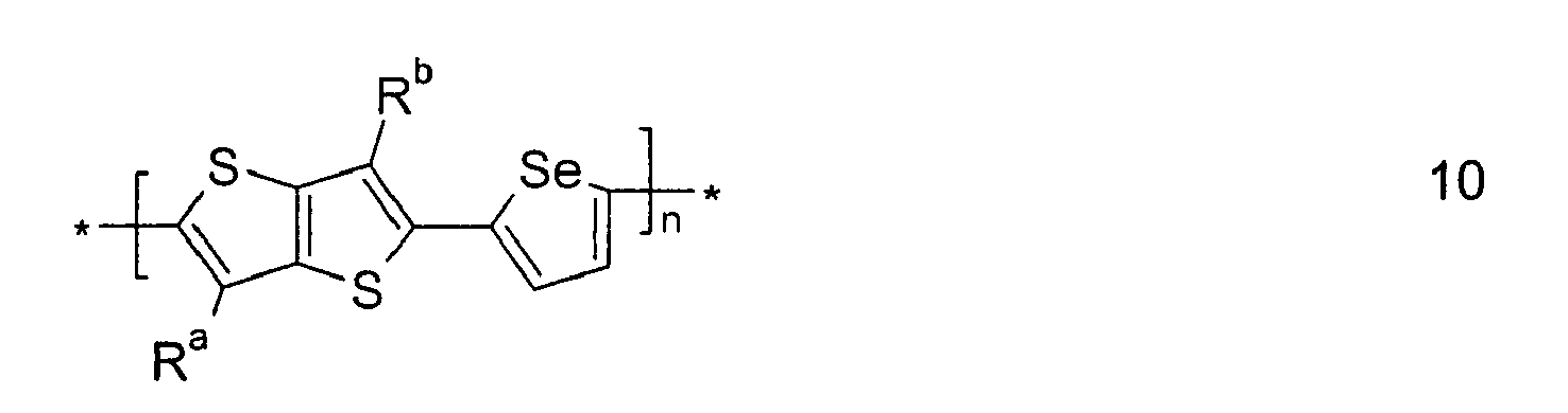
WO 2005/014691 A2 ,WO 2005/111045 A1 ,EP 1 279 689 A2 ,EP 1 279 691 A1 ,EP 1 284 276 A1 ,EP 1 398 336 A1 ,EP 1 411 563 A2 ,EP 1 439 590 A2 ,EP 1 477 504 A1 andEP 1 510 535 A1 . Very preferred are polymers of the following formulae



- Ra, Rb, Rc, Rd
- are independently of each other, and in case of multiple occurrence identical or different, selected from H, halogen, optionally substituted aryl or heteroaryl, or straight-hain, branched or cyclic alkyl with 1 to 20 C-atoms, which is optionally mono- or polysubstituted by F, Cl, Br, I or CN, and wherein one or more non-adjacent CH2 groups are optionally replaced, in each case independently from one another, by -O-, -S-, -NH-, -NR0-, -SiR0R00-, -CO-, -COO-, -OCO-, -O-CO-O-, -S-CO-, -CO-S-, -CX1=CX2- or -C≡C- in such a manner that O and/or S atoms are not linked directly to one another,
- R0 and R00
- are independently of each other H, optionally substituted aryl or alkyl with 1 to 12 C-atoms,
- X1 and X2
- are independently of each other H, F, Cl or CN,
- n
- is an integer > 1.
- Very preferably Ra-d are selected from C1-C20-alkyl that is optionally substituted with one or more fluorine atoms, C1-C20-alkenyl, C1-C20-alkynyl, C1-C20-alkoxy, C1-C20-thioalkyl, C1-C20-silyl, C1-C20-amino or C1-C20-fluoroalkyl, in particular from alkenyl, alkynyl, alkoxy, thioalkyl or fluoroalkyl, all of which are straight-chain and have 1 to 12, preferably 5 to 12 C-atoms, most preferably pentyl, hexyl, heptyl, octyl, nonyl, decyl, undecyl or dodecyl.
- The formulation according to the present invention can additionally comprise one or more further components like for example lubricating agents, wetting agents, dispersing agents, hydrophobing agents, adhesive agents, flow improvers, defoaming agents, deaerators, diluents, reactive or non-reactive diluents, auxiliaries, colourants, dyes, pigments or nanoparticles, furthermore, especially in case crosslinkable binders are used, catalysts, sensitizers, stabilizers, inhibitors, chain-transfer agents or co-reacting monomers.
- The formulation according to the present invention can be prepared by methods known in the art, for example by mixing one or more organic semiconducting compounds, one more surface-active compounds and one or more non-polar or non-alcoholic organic solvents as described above and below, or dissolving the compounds in the solvent(s).
- The semiconductor formulations according to the present invention are useful as semiconducting, electrically conducting, photoconducting or light-emitting materials in optical, electrooptical or electronic components or devices, in particular in OFETs, OPVs or sensor devices, electrophotographic recording devices, and other semiconductor applications as described above and below. They are especially suitable for use in OFETs (e.g. for RFID tags or TFT applications) and OPVs, furthermore in components of OLED structures (like charge transport or emitting layers) for lighting or display applications.
- The semiconductor formulation according to the present invention can also be used as an organic "metal" in applications including, but not limited to, charge injection layers and ITO planarising layers in organic light emitting diode applications, films for flat panel displays and touch screens, antistatic films, printed conductive substrates, patterns or tracts in electronic applications such as printed circuit boards and condensers.
- OFETs where an organic semiconductive material is arranged as a film between a gate-dielectric and a drain and a source electrode, are generally known, for example from
US 5,892,244 ,WO 00/79617 US 5,998,804 and from the references cited in the background and prior art section. Preferred applications of these FETs are for example integrated circuitry, TFT-displays and security applications. - In security applications, OFETs and other devices with semiconductive materials, like transistors or diodes, can be used for ID tags or security markings to authenticate and prevent counterfeiting of documents of value like banknotes, credit cards or ID cards, national ID documents, licenses or any product with money value, like stamps, tickets, shares, cheques and the like.
- Alternatively, the semiconductors according to the invention can be used in OLEDs, for example in displays or as backlight of displays. Conventional OLEDs are typically realized by using multilayer structures. An emission layer is usually sandwiched between one or more electron-transport and/ or hole-transport layers. By applying an electric voltage electrons and holes as charge carriers move towards the emission layer where their recombination leads to the excitation and hence luminescence of the lumophor units contained in the emission layer. The materials according to the present invention can be employed in one or more of the charge transport layers and/or in the emission layer, corresponding to their electrical and optical properties. The selection, characterization and processing of suitable monomeric, oligomeric and polymeric compounds or materials for the use in OLEDs is known to the ordinary expert and described for example in Meerholz, Synthetic Materials 111-112, 31-34 (2000) or Alcala, J. Appl. Phys. 88, 7124-7128 (2000) or the literature cited therein.
- Semiconducting films or layers can be formed by providing a formulation according to the present invention onto a substrate and, if a solvent is present, removing the solvent. This can be done by well known techniques such as spin coating, dip coating, spray coating, brush coating or doctor blade coating, as well as printing techniques including but not limited to gravure printing, ink jet printing, stamping, screen printing, letter-press printing, roller printing, reverse-roller printing, offset lithography printing, flexographic printing, web printing, pad printing or other known printing methods.
- Selected formulations of the present invention may be applied to prefabricated device substrates by ink jet printing or microdispensing. Preferably industrial piezoelectric print heads such as but not limited to those supplied by Aprion, Hitachi-Koki, InkJet Technology, On Target Technology, Picojet, Spectra, Trident, Xaar may be used to apply the organic semiconductor layer to a substrate. Additionally semi-industrial heads such as those manufactured by Brother, Epson, Konica, Seiko Instruments Toshiba TEC or single nozzle microdispensers such as those produced by Microdrop and Microfab may be used.
- In order to be applied by ink jet printing or microdispensing, the mixture of the compound of formula I and the binder should be first dissolved in a suitable solvent. Solvents must fulfill the requirements stated above and must not have any detrimental effect on the chosen print head. Additionally, solvents should have boiling points >100°C, preferably >140°C and more preferably >150°C in order to prevent operability problems caused by the solution drying out inside the print head. Suitable solvents for printing include substituted and non-substituted xylene derivatives, di-C1-2-alkyl formamide, substituted and non-substituted anisoles and other phenolether derivatives, substituted heterocycles such as substituted pyridines, pyrazines, pyrimidines, pyrrolidinones, substituted and non-substituted N,N-di-C1-2-alkylanilines and other fluorinated or chlorinated aromatics.
- Preferred formulations for ink jet printing comprise a benzene derivative which has a benzene ring substituted by one or more substituents wherein the total number of carbon atoms among the one or more substituents is at least three. For example, the benzene derivative may be substituted with a propyl group or three methyl groups, in either case there being at least three carbon atoms in total. Such a solvent enables an ink jet fluid to be formed comprising the solvent with the binder and the OSC compound which reduces or prevents clogging of the jets and separation of the components during spraying. The solvent(s) may include those selected from the following list of examples: dodecylbenzene, 1-methyl-4-tert-butylbenzene, terpineol limonene, isodurene, terpinolene, cymene, diethylbenzene. The solvent may be a solvent mixture, that is a combination of two or more solvents, each solvent preferably having a boiling point >100°C, more preferably >140°C. Such solvent(s) also enhance film formation in the layer deposited and reduce defects in the layer.
- The ink jet fluid (that is mixture of solvent, surfactant and semiconducting compound) preferably has a viscosity at 20°C of 1-100mPa·s, more preferably 1-50mPa·s and most preferably 1-30mPa·s.
- The semiconducting layer in a device according to the present invention is typically at most 1 micron (=1µm) thick, although it may be thicker if required. The exact thickness of the layer will depend, for example, upon the requirements of the electronic device in which the layer is used. For use in an OFET or OLED, the layer thickness may typically be 500 nm or less.
- The substrate used for preparing an OSC layer may include any underlying device layer, electrode or separate substrate such as silicon wafer, glass or polymer substrate for example.
- An OFET device according to the present invention preferably comprises:
- a source electrode,
- a drain electrode,
- a gate electrode,
- an OSC layer as described above,
- one or more gate insulator layers,
- optionally a substrate,
- The gate, source and drain electrodes and the insulating and semiconducting layer in the OFET device may be arranged in any sequence, provided that the source and drain electrode are separated from the gate electrode by the insulating layer, the gate electrode and the semiconductor layer both contact the insulating layer, and the source electrode and the drain electrode both contact the semiconducting layer.
- The OFET device can be a top gate device or a bottom gate device. Suitable structures and manufacturing methods of an OFET device are known to the skilled in the art and are described in the literature, for example in
WO 03/052841 - The gate insulator layer preferably comprises a fluoropolymer, like e.g. the commercially available Cytop 809M® or Cytop 107M® (from Asahi Glass). Preferably the gate insulator layer is deposited, e.g. by spin-coating, doctor blading, wire bar coating, spray or dip coating or other known methods, from a formulation comprising an insulator material and one or more solvents with one or more fluoro atoms (fluorosolvents), preferably a perfluorosolvent. A suitable perfluorosolvent is e.g. FC75® (available from Acros, catalogue number 12380). Other suitable fluoropolymers and fluorosolvents are known in prior art, like for example the perfluoropolymers Teflon AF® 1600 or 2400 (from DuPont) or Fluoropel® (from Cytonix) or the perfluorosolvent FC 43® (Acros, No. 12377).
- Throughout the description and claims of this specification, unless the context clearly indicates otherwise, as used herein plural forms of the terms herein are to be construed as including the singular form and vice versa. The words "comprise" and "contain" and variations of the words, for example "comprising" and "comprises", mean "including but not limited to", and are not intended to (and do not) exclude other components.
- It will be appreciated that variations to the foregoing embodiments of the invention can be made while still falling within the scope of the invention. Each feature disclosed in this specification, unless stated otherwise, may be replaced by alternative features serving the same, equivalent or similar purpose. Thus, unless stated otherwise, each feature disclosed is one example only of a generic series of equivalent or similar features.
- All of the features disclosed in this specification may be combined in any combination, except combinations where at least some of such features and/or steps are mutually exclusive. In particular, the preferred features of the invention are applicable to all aspects of the invention and may be used in any combination. Likewise, features described in non-essential combinations may be used separately (not in combination).
- It will be appreciated that many of the features described above, particularly of the preferred embodiments, are inventive in their own right and not just as part of an embodiment of the present invention. Independent protection may be sought for these features in addition to or alternative to any invention presently claimed.
- The invention will now be described in more detail by reference to the following examples, which are illustrative only and do not limit the scope of the invention.
- Unless stated otherwise, in the foregoing and the following, all temperatures are given in degrees Celsius, and all percentages are by weight. All specific values of physical parameters like the permittivity (ε), charge carrier mobility (µ), solubility parameter (δ) and viscosity (η) as given above and below refer to a temperature of 20°C (+/- 1°C). Ratios of monomers or repeating units in polymers are given in mol %. Ratios of polymers in polymer blends are given in weight %. The molecular weight of polymers is given as weight average molecular weight Mw (GPC, polystyrene standard).
- The Hansen parameter is determined as described in " Hansen Solubility Parameters: A User's Handbook' by Charles M. Hansen; CRC Press 1999; ISBN 0 849 315255.
- Formulation viscosities are obtained using an automated microviscometer (available for example from Anton Paar GmbH, Graz, Austria), which is based on the rolling/falling ball principle. A capillary is used in which a small metal ball rolls and by tilting this one way or the other the ball will descent through the liquid and can be timed. The length of time taken to pass a set distance through the liquid is proportional to the viscosity and the angle at which the tube is held at during this determines the shear rate of the measurement - which, for a Newtonian liquid, should not affect the recorded viscosity.
- A polymer based FET is prepared from a formulation containing the following semiconducting polymer P1 from 0.2 to 10% and 0.01 % of silane (OTS) in xylene as organic solvent.

- The synthesis of P1 is described in
EP 1 510 535 A1 . - The warm formulation is deposited onto an ozone-cleaned (hydrophilic) Si/SiO2 FET substrate with pre-defined gold source-drain electrodes and common Si-gate. After ~15min the substrate is spun, resulting in a formation of a thin film of polymer P1 on the FET substrate. A control sample is prepared from the pristine P1-polymer solution in xylene following the same procedure as the above sample. The electrical characterization of the transistor devices was carried out in dry nitrogen atmosphere using computer controlled Agilent 4155C Semiconductor Parameter Analyser. Field-effect mobility was calculated in saturation regime, where drain current is expressed as:

where W is the channel width, L the channel length, Ci the capacitance of insulating layer, Vg the gate voltage, Vth the threshold voltage. - Vth is estimated from linear fit of

Table 1 - Electrical properties of OFETs fabricated from pristine polymer solution and from formulation containing OTS FET On Current (A); FET Mobility (cm2/Vs); On/Off ratio Saturated regime Saturated regime Pristine With OTS Pristine With OTS Pristine With OTS 2×10⁴ 9×10⁴ 7.2×10⁻⁶ 6.0×10⁻⁵ 5.2×10⁴ 4.7×10⁻³ - As can be seen from table 1, the use of a formulation according to the invention comprising the surfactant OTS increases the FET On Current and FET Mobility at ~10 times, compared to the pristine solution without OTS.
Claims (23)
- Formulation comprising one or more organic semiconducting compounds, one more surface-active compounds and one or more solvents selected from non-polar or non-alcoholic organic solvents.
- Formulation according to claim 1, characterized in that it is a homogeneous solution.
- Formulation according to claim 1 or 2, characterized in that the surfactants are monomeric or small-molecule compounds.
- Formulation according to one or more of claims 1 to 3, characterized in that the surfactants are selected from hydrophobic surfactants containing a head group capable of forming a covalent bond or a stable adsorption product with an active substrate, such as a chlorosilane, silazane or a thiol group, and further comprising a tail group selected from alkyl, fluoroalkyl or siloxane groups.
- Formulation according to one or more of claims 1 to 4, characterized in that the surfactants are selected from compounds comprising hydrocarbon, fluorocarbon, siloxane or silane groups.
- Formulation according to one or more of claims 1 to 5, characterized in that the surfactants are selected from silanes or silazanes.
- Formulation according to claim 6, characterized in that the surfactants are selected from HMDS (1,1,1,3,3,3-Hexamethyldisilazane), OTS (octyl trichlorosilane), ODTS (octadecyl trichloro silane), fluorocarbon silanes, 1 H-,1 H-,2H-,2H-perfluorooctyldimethylsilane, or optionally substituted trichlorosilanes.
- Formulation according to one or more of claims 1 to 7, characterized in that the concentration of the surfactants is from 10-5 to 5 wt. %.
- Formulation according to one or more of claims 1 to 8, characterized in that the organic semiconducting compounds are p-type organic semiconductors.
- Formulation according to one or more of claims 1 to 9, characterized in that the organic semiconducting compounds are selected from polymers with conjugated pi-systems.
- Formulation according to one or more of claims 1 to 10, characterized in that the organic semiconducting compounds are selected from polyphenylenevinylene (PPV), polyarylenevinylene (PAV), polyparaphenylene (PPP), polypyridine (PPy), polypyridinevinylene (PPyV), polythiophene (PT), polyalkylthiophene (PAT), polyfluorene (PF), polyspirobifluorene (PSF), polypyrrole, polyvinylcarbazole, polytriarylamine, polyacetylene, polyphenylene sulfide, polythienylene vinylene, polyisothianaphthene, polyazulene, polyfuran, polyaniline, polyselenophene, polyindenofluorene, all of which are substituted or unsubstituted, or mixtures, blends, statistical or defined copolymers or block copolymers of the above.
- Formulation according to one or more of claims 1 to 11, characterized in that the organic semiconducting compounds are selected from polymers or copolymers comprising one or more units selected from optionally substituted thiophene, optionally substituted selenophene, 3-alkylthiophene, optionally substituted [3,2b]-thienothiophene, optionally substituted [2,3b]-thienothiophene and optionally substituted dithienotiophene.
- Formulation according to one or more of claims 1 to 11, characterized in that the organic semiconducting compounds are selected from the following formulae


 Ra, Rb, Rc, Rd are independently of each other, and in case of multiple occurrence identical or different, selected from H, halogen, optionally substituted aryl or heteroaryl, or straight-hain, branched or cyclic alkyl with 1 to 20 C-atoms, which is optionally mono- or polysubstituted by F, Cl, Br, I or CN, and wherein one or more non-adjacent CH2 groups are optionally replaced, in each case independently from one another, by -O-, -S-, -NH-, -NR0-, -SiR0R00-, -CO-, -COO-, -OCO-, -O-CO-O-, -S-CO-, -CO-S-, -CX1=CX2- or -C≡C- in such a manner that O and/or S atoms are not linked directly to one another,R0 and R00 are independently of each other H, optionally substituted aryl or alkyl with 1 to 12 C-atoms,X1 and X2 are independently of each other H, F, Cl or CN,n is an integer > 1.
 - Formulation according to one or more of claims 1 to 13, characterized in that the concentration of the organic semiconducting compounds is from 0.1 to 10 %.
- Formulation according to one or more of claims 1 to 14, characterized in that the solvents are selected from solvents having a polar contribution to the Hansen solubility parameter of < 6 Mpa 1/2.
- Formulation according to one or more of claims 1 to 15, characterized in that the organic solvents are selected from non-alcoholic aliphatic and aromatic hydrocarbons, halogenated aliphatic and aromatic hydrocarbons.
- Formulation according to one or more of claims 1 to 16, characterized in that the organic solvents are selected from xylene, toluene, benzene, tetralin, indane, xylene, dichlorobenzene, chloroform, dichloromethane, cyclohexane, anisole, N-methyl-2-pyrrolidone (NMP), dimethyl sulfoxide (DMSO), cyclohexanone, dioxane, tetrahydrofuran (THF), γ-butyrolactone or mixtures thereof.
- Organic semiconductor layer obtainable by providing a formulation according to one or more of claims 1 to 17 onto a substrate and optionally removing the solvent.
- Use of a formulation or layer according to one or more of claims 1 to 18 as semiconducting, electrically conducting, photoconducting or light-emitting material in optical, electrooptical or electronic components or devices, organic field effect transistors (OFET), integrated circuitry (IC), thin film transistors (TFT), flat panel displays, radio frequency identification (RFID) tags, electroluminescent or photoluminescent devices or components, organic light emitting diodes (OLED), backlights of displays, organic photovoltaic devices (OPVs), sensor devices, charge injection layers, Schottky diodes, planarising layers, antistatic films, conducting substrates or patterns, electrode materials in batteries, photoconductors, electrophotographic applications, electrophotographic recording, organic memory devices, alignment layers, cosmetic or pharmaceutical compositions or for detecting and discriminating DNA sequences.
- Semiconducting, electrically conducting, photoconducting or light-emitting component or device, characterized in that it comprises a formulation or layer according to one or more of claims 1 to 18.
- Component or device according to claim 20, characterized in that it is an IC, OFET, TFT, OPV, RFID tag or OLED.
- Security marking or device, characterized in that it comprises an OFET or RFID tag according to claim 21.
- Method of preparing a formulation according to one or more of claims 1 to 17, by mixing one or more organic semiconducting compounds, one more surface-active compounds and one or more non-polar or non-alcoholic organic solvents as defined in one or more of claims 1 to 17.
Priority Applications (1)
| Application Number | Priority Date | Filing Date | Title |
|---|---|---|---|
| EP07004110A EP1837928B1 (en) | 2006-03-24 | 2007-02-28 | Organic semiconductor formulation |
Applications Claiming Priority (2)
| Application Number | Priority Date | Filing Date | Title |
|---|---|---|---|
| EP06006093 | 2006-03-24 | ||
| EP07004110A EP1837928B1 (en) | 2006-03-24 | 2007-02-28 | Organic semiconductor formulation |
Publications (2)
| Publication Number | Publication Date |
|---|---|
| EP1837928A1 true EP1837928A1 (en) | 2007-09-26 |
| EP1837928B1 EP1837928B1 (en) | 2010-06-09 |
Family
ID=38001756
Family Applications (1)
| Application Number | Title | Priority Date | Filing Date |
|---|---|---|---|
| EP07004110A Active EP1837928B1 (en) | 2006-03-24 | 2007-02-28 | Organic semiconductor formulation |
Country Status (1)
| Country | Link |
|---|---|
| EP (1) | EP1837928B1 (en) |
Cited By (3)
| Publication number | Priority date | Publication date | Assignee | Title |
|---|---|---|---|---|
| WO2011076324A1 (en) * | 2009-12-23 | 2011-06-30 | Merck Patent Gmbh | Compositions comprising organic semiconducting compounds |
| US9178156B2 (en) | 2009-12-23 | 2015-11-03 | Merck Patent Gmbh | Compositions comprising polymeric binders |
| CN108129661A (en) * | 2018-01-03 | 2018-06-08 | 京东方科技集团股份有限公司 | A kind of polymer, quantum dot film layer and preparation method thereof |
Citations (5)
| Publication number | Priority date | Publication date | Assignee | Title |
|---|---|---|---|---|
| EP1275650A2 (en) * | 2001-07-09 | 2003-01-15 | MERCK PATENT GmbH | Thienthiophenes with polymerisable group |
| WO2003050147A1 (en) * | 2001-12-13 | 2003-06-19 | MAX-PLANCK-Gesellschaft zur Förderung der Wissenschaften e.V. | Nanostructured layers on the basis of nanoparticles of organic semiconductors |
| WO2005057677A1 (en) * | 2003-12-09 | 2005-06-23 | Showa Denko K.K | Polymer for anode buffer layer, coating solution for anode buffer layer, and organic light emitting device |
| EP1564251A1 (en) * | 2004-02-10 | 2005-08-17 | H.C. Starck GmbH | Polythiophene compositions for improving organic light-emitting diodes |
| US20050236614A1 (en) * | 2004-04-22 | 2005-10-27 | Parker Ian D | Processes for forming organic layers, organic electronic devices, and transistors |
-
2007
- 2007-02-28 EP EP07004110A patent/EP1837928B1/en active Active
Patent Citations (5)
| Publication number | Priority date | Publication date | Assignee | Title |
|---|---|---|---|---|
| EP1275650A2 (en) * | 2001-07-09 | 2003-01-15 | MERCK PATENT GmbH | Thienthiophenes with polymerisable group |
| WO2003050147A1 (en) * | 2001-12-13 | 2003-06-19 | MAX-PLANCK-Gesellschaft zur Förderung der Wissenschaften e.V. | Nanostructured layers on the basis of nanoparticles of organic semiconductors |
| WO2005057677A1 (en) * | 2003-12-09 | 2005-06-23 | Showa Denko K.K | Polymer for anode buffer layer, coating solution for anode buffer layer, and organic light emitting device |
| EP1564251A1 (en) * | 2004-02-10 | 2005-08-17 | H.C. Starck GmbH | Polythiophene compositions for improving organic light-emitting diodes |
| US20050236614A1 (en) * | 2004-04-22 | 2005-10-27 | Parker Ian D | Processes for forming organic layers, organic electronic devices, and transistors |
Non-Patent Citations (1)
| Title |
|---|
| SIRRINGHAUS H ET AL: "INTEGRATED, HIGH-MOBILITY POLYMER FIELD-EFFECT TRANSISTORS DRIVING POLYMER LIGHT-EMITTING DIODES", SYNTHETIC METALS, ELSEVIER SEQUOIA, LAUSANNE, CH, vol. 102, June 1999 (1999-06-01), pages 857 - 860, XP000934322, ISSN: 0379-6779 * |
Cited By (5)
| Publication number | Priority date | Publication date | Assignee | Title |
|---|---|---|---|---|
| WO2011076324A1 (en) * | 2009-12-23 | 2011-06-30 | Merck Patent Gmbh | Compositions comprising organic semiconducting compounds |
| US9178156B2 (en) | 2009-12-23 | 2015-11-03 | Merck Patent Gmbh | Compositions comprising polymeric binders |
| US9368761B2 (en) | 2009-12-23 | 2016-06-14 | Merck Patent Gmbh | Compositions comprising organic semiconducting compounds |
| CN108129661A (en) * | 2018-01-03 | 2018-06-08 | 京东方科技集团股份有限公司 | A kind of polymer, quantum dot film layer and preparation method thereof |
| US11233212B2 (en) | 2018-01-03 | 2022-01-25 | Boe Technology Group Co., Ltd. | Polymer, quantum dots film layer and preparation method thereof |
Also Published As
| Publication number | Publication date |
|---|---|
| EP1837928B1 (en) | 2010-06-09 |
Similar Documents
| Publication | Publication Date | Title |
|---|---|---|
| US8314416B2 (en) | Organic semiconductor formulation | |
| KR101932806B1 (en) | Organic semiconductor formulation | |
| US7332369B2 (en) | Organic electronic devices | |
| US8049209B2 (en) | Thin-film transistors | |
| US8455373B2 (en) | Ink-jet print ink and organic thin film transistor using thereof | |
| EP1747595A1 (en) | Formulation for ink-jet printing comprising semiconducting polymers | |
| EP1837928B1 (en) | Organic semiconductor formulation | |
| JP6465799B2 (en) | Organic semiconductor compound | |
| US10164191B2 (en) | Methoxyaryl surface modifier and organic electronic devices comprising such methoxyaryl surface modifier | |
| WO2018029160A1 (en) | Method to achieve efficient charge injection for electron and/or hole transport in semiconducting layers | |
| US7563860B2 (en) | Semiconductors and electronic devices generated therefrom | |
| JP2012023370A (en) | Use as charge transport material of poly-3,3"-dialkyl-2,2':5'2"-terthiophene | |
| US7615607B2 (en) | Semiconductor polymers | |
| HK1148609A (en) | Organic semiconductor formulation |
Legal Events
| Date | Code | Title | Description |
|---|---|---|---|
| PUAI | Public reference made under article 153(3) epc to a published international application that has entered the european phase |
Free format text: ORIGINAL CODE: 0009012 |
|
| 17P | Request for examination filed |
Effective date: 20070228 |
|
| AK | Designated contracting states |
Kind code of ref document: A1 Designated state(s): AT BE BG CH CY CZ DE DK EE ES FI FR GB GR HU IE IS IT LI LT LU LV MC NL PL PT RO SE SI SK TR |
|
| AX | Request for extension of the european patent |
Extension state: AL BA HR MK YU |
|
| 17Q | First examination report despatched |
Effective date: 20080317 |
|
| AKX | Designation fees paid |
Designated state(s): AT BE BG CH CY CZ DE DK EE ES FI FR GB GR HU IE IS IT LI LT LU LV MC NL PL PT RO SE SI SK TR |
|
| GRAP | Despatch of communication of intention to grant a patent |
Free format text: ORIGINAL CODE: EPIDOSNIGR1 |
|
| GRAS | Grant fee paid |
Free format text: ORIGINAL CODE: EPIDOSNIGR3 |
|
| GRAA | (expected) grant |
Free format text: ORIGINAL CODE: 0009210 |
|
| AK | Designated contracting states |
Kind code of ref document: B1 Designated state(s): AT BE BG CH CY CZ DE DK EE ES FI FR GB GR HU IE IS IT LI LT LU LV MC NL PL PT RO SE SI SK TR |
|
| REG | Reference to a national code |
Ref country code: CH Ref legal event code: EP |
|
| REG | Reference to a national code |
Ref country code: IE Ref legal event code: FG4D |
|
| REF | Corresponds to: |
Ref document number: 602007007003 Country of ref document: DE Date of ref document: 20100722 Kind code of ref document: P |
|
| REG | Reference to a national code |
Ref country code: DE Ref legal event code: R096 Ref document number: 602007007003 Country of ref document: DE Effective date: 20100722 |
|
| REG | Reference to a national code |
Ref country code: NL Ref legal event code: VDEP Effective date: 20100609 |
|
| PG25 | Lapsed in a contracting state [announced via postgrant information from national office to epo] |
Ref country code: SE Free format text: LAPSE BECAUSE OF FAILURE TO SUBMIT A TRANSLATION OF THE DESCRIPTION OR TO PAY THE FEE WITHIN THE PRESCRIBED TIME-LIMIT Effective date: 20100609 Ref country code: LT Free format text: LAPSE BECAUSE OF FAILURE TO SUBMIT A TRANSLATION OF THE DESCRIPTION OR TO PAY THE FEE WITHIN THE PRESCRIBED TIME-LIMIT Effective date: 20100609 |
|
| LTIE | Lt: invalidation of european patent or patent extension |
Effective date: 20100609 |
|
| PG25 | Lapsed in a contracting state [announced via postgrant information from national office to epo] |
Ref country code: AT Free format text: LAPSE BECAUSE OF FAILURE TO SUBMIT A TRANSLATION OF THE DESCRIPTION OR TO PAY THE FEE WITHIN THE PRESCRIBED TIME-LIMIT Effective date: 20100609 Ref country code: FI Free format text: LAPSE BECAUSE OF FAILURE TO SUBMIT A TRANSLATION OF THE DESCRIPTION OR TO PAY THE FEE WITHIN THE PRESCRIBED TIME-LIMIT Effective date: 20100609 Ref country code: SI Free format text: LAPSE BECAUSE OF FAILURE TO SUBMIT A TRANSLATION OF THE DESCRIPTION OR TO PAY THE FEE WITHIN THE PRESCRIBED TIME-LIMIT Effective date: 20100609 Ref country code: LV Free format text: LAPSE BECAUSE OF FAILURE TO SUBMIT A TRANSLATION OF THE DESCRIPTION OR TO PAY THE FEE WITHIN THE PRESCRIBED TIME-LIMIT Effective date: 20100609 |
|
| PG25 | Lapsed in a contracting state [announced via postgrant information from national office to epo] |
Ref country code: PL Free format text: LAPSE BECAUSE OF FAILURE TO SUBMIT A TRANSLATION OF THE DESCRIPTION OR TO PAY THE FEE WITHIN THE PRESCRIBED TIME-LIMIT Effective date: 20100609 Ref country code: CY Free format text: LAPSE BECAUSE OF FAILURE TO SUBMIT A TRANSLATION OF THE DESCRIPTION OR TO PAY THE FEE WITHIN THE PRESCRIBED TIME-LIMIT Effective date: 20100609 |
|
| PG25 | Lapsed in a contracting state [announced via postgrant information from national office to epo] |
Ref country code: NL Free format text: LAPSE BECAUSE OF FAILURE TO SUBMIT A TRANSLATION OF THE DESCRIPTION OR TO PAY THE FEE WITHIN THE PRESCRIBED TIME-LIMIT Effective date: 20100609 Ref country code: EE Free format text: LAPSE BECAUSE OF FAILURE TO SUBMIT A TRANSLATION OF THE DESCRIPTION OR TO PAY THE FEE WITHIN THE PRESCRIBED TIME-LIMIT Effective date: 20100609 Ref country code: GR Free format text: LAPSE BECAUSE OF FAILURE TO SUBMIT A TRANSLATION OF THE DESCRIPTION OR TO PAY THE FEE WITHIN THE PRESCRIBED TIME-LIMIT Effective date: 20100910 |
|
| PG25 | Lapsed in a contracting state [announced via postgrant information from national office to epo] |
Ref country code: CZ Free format text: LAPSE BECAUSE OF FAILURE TO SUBMIT A TRANSLATION OF THE DESCRIPTION OR TO PAY THE FEE WITHIN THE PRESCRIBED TIME-LIMIT Effective date: 20100609 Ref country code: SK Free format text: LAPSE BECAUSE OF FAILURE TO SUBMIT A TRANSLATION OF THE DESCRIPTION OR TO PAY THE FEE WITHIN THE PRESCRIBED TIME-LIMIT Effective date: 20100609 Ref country code: RO Free format text: LAPSE BECAUSE OF FAILURE TO SUBMIT A TRANSLATION OF THE DESCRIPTION OR TO PAY THE FEE WITHIN THE PRESCRIBED TIME-LIMIT Effective date: 20100609 Ref country code: PT Free format text: LAPSE BECAUSE OF FAILURE TO SUBMIT A TRANSLATION OF THE DESCRIPTION OR TO PAY THE FEE WITHIN THE PRESCRIBED TIME-LIMIT Effective date: 20101011 Ref country code: IS Free format text: LAPSE BECAUSE OF FAILURE TO SUBMIT A TRANSLATION OF THE DESCRIPTION OR TO PAY THE FEE WITHIN THE PRESCRIBED TIME-LIMIT Effective date: 20101009 Ref country code: BE Free format text: LAPSE BECAUSE OF FAILURE TO SUBMIT A TRANSLATION OF THE DESCRIPTION OR TO PAY THE FEE WITHIN THE PRESCRIBED TIME-LIMIT Effective date: 20100609 |
|
| PG25 | Lapsed in a contracting state [announced via postgrant information from national office to epo] |
Ref country code: IT Free format text: LAPSE BECAUSE OF FAILURE TO SUBMIT A TRANSLATION OF THE DESCRIPTION OR TO PAY THE FEE WITHIN THE PRESCRIBED TIME-LIMIT Effective date: 20100609 |
|
| PLBE | No opposition filed within time limit |
Free format text: ORIGINAL CODE: 0009261 |
|
| STAA | Information on the status of an ep patent application or granted ep patent |
Free format text: STATUS: NO OPPOSITION FILED WITHIN TIME LIMIT |
|
| PG25 | Lapsed in a contracting state [announced via postgrant information from national office to epo] |
Ref country code: DK Free format text: LAPSE BECAUSE OF FAILURE TO SUBMIT A TRANSLATION OF THE DESCRIPTION OR TO PAY THE FEE WITHIN THE PRESCRIBED TIME-LIMIT Effective date: 20100609 |
|
| REG | Reference to a national code |
Ref country code: DE Ref legal event code: R097 Ref document number: 602007007003 Country of ref document: DE Effective date: 20110309 Ref country code: DE Ref legal event code: R097 Ref document number: 602007007003 Country of ref document: DE Effective date: 20110310 |
|
| PG25 | Lapsed in a contracting state [announced via postgrant information from national office to epo] |
Ref country code: MC Free format text: LAPSE BECAUSE OF NON-PAYMENT OF DUE FEES Effective date: 20110228 |
|
| REG | Reference to a national code |
Ref country code: CH Ref legal event code: PL |
|
| PG25 | Lapsed in a contracting state [announced via postgrant information from national office to epo] |
Ref country code: CH Free format text: LAPSE BECAUSE OF NON-PAYMENT OF DUE FEES Effective date: 20110228 Ref country code: LI Free format text: LAPSE BECAUSE OF NON-PAYMENT OF DUE FEES Effective date: 20110228 |
|
| REG | Reference to a national code |
Ref country code: FR Ref legal event code: ST Effective date: 20111102 |
|
| REG | Reference to a national code |
Ref country code: IE Ref legal event code: MM4A |
|
| PG25 | Lapsed in a contracting state [announced via postgrant information from national office to epo] |
Ref country code: FR Free format text: LAPSE BECAUSE OF NON-PAYMENT OF DUE FEES Effective date: 20110228 Ref country code: IE Free format text: LAPSE BECAUSE OF NON-PAYMENT OF DUE FEES Effective date: 20110228 |
|
| PG25 | Lapsed in a contracting state [announced via postgrant information from national office to epo] |
Ref country code: LU Free format text: LAPSE BECAUSE OF NON-PAYMENT OF DUE FEES Effective date: 20110228 |
|
| PG25 | Lapsed in a contracting state [announced via postgrant information from national office to epo] |
Ref country code: BG Free format text: LAPSE BECAUSE OF FAILURE TO SUBMIT A TRANSLATION OF THE DESCRIPTION OR TO PAY THE FEE WITHIN THE PRESCRIBED TIME-LIMIT Effective date: 20100909 Ref country code: TR Free format text: LAPSE BECAUSE OF FAILURE TO SUBMIT A TRANSLATION OF THE DESCRIPTION OR TO PAY THE FEE WITHIN THE PRESCRIBED TIME-LIMIT Effective date: 20100609 |
|
| PG25 | Lapsed in a contracting state [announced via postgrant information from national office to epo] |
Ref country code: HU Free format text: LAPSE BECAUSE OF FAILURE TO SUBMIT A TRANSLATION OF THE DESCRIPTION OR TO PAY THE FEE WITHIN THE PRESCRIBED TIME-LIMIT Effective date: 20100609 Ref country code: ES Free format text: LAPSE BECAUSE OF FAILURE TO SUBMIT A TRANSLATION OF THE DESCRIPTION OR TO PAY THE FEE WITHIN THE PRESCRIBED TIME-LIMIT Effective date: 20100920 |
|
| REG | Reference to a national code |
Ref country code: GB Ref legal event code: 732E Free format text: REGISTERED BETWEEN 20200312 AND 20200318 |
|
| REG | Reference to a national code |
Ref country code: DE Ref legal event code: R079 Ref document number: 602007007003 Country of ref document: DE Free format text: PREVIOUS MAIN CLASS: H01L0051000000 Ipc: H10K0099000000 |
|
| REG | Reference to a national code |
Ref country code: GB Ref legal event code: 732E Free format text: REGISTERED BETWEEN 20230504 AND 20230510 |
|
| P01 | Opt-out of the competence of the unified patent court (upc) registered |
Effective date: 20230528 |
|
| REG | Reference to a national code |
Ref country code: DE Ref legal event code: R081 Ref document number: 602007007003 Country of ref document: DE Owner name: FLEXENABLE TECHNOLOGY LTD., GB Free format text: FORMER OWNER: MERCK PATENT GMBH, 64293 DARMSTADT, DE |
|
| PGFP | Annual fee paid to national office [announced via postgrant information from national office to epo] |
Ref country code: DE Payment date: 20250821 Year of fee payment: 19 |
|
| PGFP | Annual fee paid to national office [announced via postgrant information from national office to epo] |
Ref country code: GB Payment date: 20250819 Year of fee payment: 19 |