EP1510535A1 - Mono-, Oligo- and Polythieno(2,3-b)thiophenes - Google Patents
Mono-, Oligo- and Polythieno(2,3-b)thiophenes Download PDFInfo
- Publication number
- EP1510535A1 EP1510535A1 EP04018079A EP04018079A EP1510535A1 EP 1510535 A1 EP1510535 A1 EP 1510535A1 EP 04018079 A EP04018079 A EP 04018079A EP 04018079 A EP04018079 A EP 04018079A EP 1510535 A1 EP1510535 A1 EP 1510535A1
- Authority
- EP
- European Patent Office
- Prior art keywords
- mono
- oligo
- formula
- polymerisable
- polymers
- Prior art date
- Legal status (The legal status is an assumption and is not a legal conclusion. Google has not performed a legal analysis and makes no representation as to the accuracy of the status listed.)
- Granted
Links
- 229930192474 thiophene Natural products 0.000 title description 14
- 150000003577 thiophenes Chemical class 0.000 title description 3
- 229920000642 polymer Polymers 0.000 claims abstract description 93
- 239000000463 material Substances 0.000 claims abstract description 77
- 239000004973 liquid crystal related substance Substances 0.000 claims abstract description 35
- 239000004065 semiconductor Substances 0.000 claims abstract description 24
- 230000005669 field effect Effects 0.000 claims abstract description 13
- 230000003287 optical effect Effects 0.000 claims abstract description 11
- 239000010409 thin film Substances 0.000 claims abstract description 7
- -1 2,5-dimethoxy-1,4-phenylene Chemical group 0.000 claims description 39
- 150000001875 compounds Chemical class 0.000 claims description 39
- 125000000325 methylidene group Chemical group [H]C([H])=* 0.000 claims description 35
- 238000006243 chemical reaction Methods 0.000 claims description 24
- 239000010408 film Substances 0.000 claims description 22
- 125000004432 carbon atom Chemical group C* 0.000 claims description 18
- 125000000217 alkyl group Chemical group 0.000 claims description 17
- 229910052801 chlorine Inorganic materials 0.000 claims description 14
- 229910052731 fluorine Inorganic materials 0.000 claims description 13
- 125000001072 heteroaryl group Chemical group 0.000 claims description 13
- 229910052698 phosphorus Inorganic materials 0.000 claims description 13
- 125000003118 aryl group Chemical group 0.000 claims description 12
- 239000000178 monomer Substances 0.000 claims description 12
- 229910052794 bromium Inorganic materials 0.000 claims description 10
- 229910052740 iodine Inorganic materials 0.000 claims description 10
- 125000000732 arylene group Chemical group 0.000 claims description 9
- 125000001140 1,4-phenylene group Chemical group [H]C1=C([H])C([*:2])=C([H])C([H])=C1[*:1] 0.000 claims description 8
- 125000005549 heteroarylene group Chemical group 0.000 claims description 8
- 125000003837 (C1-C20) alkyl group Chemical group 0.000 claims description 7
- 229910052736 halogen Inorganic materials 0.000 claims description 7
- 150000002367 halogens Chemical class 0.000 claims description 7
- 125000003107 substituted aryl group Chemical group 0.000 claims description 7
- 239000000758 substrate Substances 0.000 claims description 7
- 239000007788 liquid Substances 0.000 claims description 6
- 125000004430 oxygen atom Chemical group O* 0.000 claims description 5
- 125000006850 spacer group Chemical group 0.000 claims description 5
- 125000004434 sulfur atom Chemical group 0.000 claims description 5
- 125000003860 C1-C20 alkoxy group Chemical group 0.000 claims description 4
- ZCQWOFVYLHDMMC-UHFFFAOYSA-N Oxazole Chemical compound C1=COC=N1 ZCQWOFVYLHDMMC-UHFFFAOYSA-N 0.000 claims description 4
- 125000001153 fluoro group Chemical group F* 0.000 claims description 4
- 229920006254 polymer film Polymers 0.000 claims description 4
- JUJWROOIHBZHMG-UHFFFAOYSA-N pyridine Substances C1=CC=NC=C1 JUJWROOIHBZHMG-UHFFFAOYSA-N 0.000 claims description 4
- 229920000106 Liquid crystal polymer Polymers 0.000 claims description 3
- 239000004977 Liquid-crystal polymers (LCPs) Substances 0.000 claims description 3
- FZWLAAWBMGSTSO-UHFFFAOYSA-N Thiazole Chemical class C1=CSC=N1 FZWLAAWBMGSTSO-UHFFFAOYSA-N 0.000 claims description 3
- 125000003545 alkoxy group Chemical group 0.000 claims description 3
- 239000004305 biphenyl Substances 0.000 claims description 3
- WBLIXGSTEMXDSM-UHFFFAOYSA-N chloromethane Chemical compound Cl[CH2] WBLIXGSTEMXDSM-UHFFFAOYSA-N 0.000 claims description 3
- 239000007772 electrode material Substances 0.000 claims description 3
- URMVZUQDPPDABD-UHFFFAOYSA-N thieno[2,3-f][1]benzothiole Chemical class C1=C2SC=CC2=CC2=C1C=CS2 URMVZUQDPPDABD-UHFFFAOYSA-N 0.000 claims description 3
- 125000004453 alkoxycarbonyl group Chemical group 0.000 claims description 2
- 125000004448 alkyl carbonyl group Chemical group 0.000 claims description 2
- 125000004435 hydrogen atom Chemical group [H]* 0.000 claims description 2
- 238000002347 injection Methods 0.000 claims description 2
- 239000007924 injection Substances 0.000 claims description 2
- 239000012788 optical film Substances 0.000 abstract description 2
- 239000000243 solution Substances 0.000 description 50
- OKKJLVBELUTLKV-UHFFFAOYSA-N Methanol Chemical compound OC OKKJLVBELUTLKV-UHFFFAOYSA-N 0.000 description 48
- HEDRZPFGACZZDS-MICDWDOJSA-N Trichloro(2H)methane Chemical compound [2H]C(Cl)(Cl)Cl HEDRZPFGACZZDS-MICDWDOJSA-N 0.000 description 38
- HEDRZPFGACZZDS-UHFFFAOYSA-N Chloroform Chemical compound ClC(Cl)Cl HEDRZPFGACZZDS-UHFFFAOYSA-N 0.000 description 32
- WYURNTSHIVDZCO-UHFFFAOYSA-N Tetrahydrofuran Chemical compound C1CCOC1 WYURNTSHIVDZCO-UHFFFAOYSA-N 0.000 description 32
- IJGRMHOSHXDMSA-UHFFFAOYSA-N Atomic nitrogen Chemical compound N#N IJGRMHOSHXDMSA-UHFFFAOYSA-N 0.000 description 28
- VYPSYNLAJGMNEJ-UHFFFAOYSA-N Silicium dioxide Chemical compound O=[Si]=O VYPSYNLAJGMNEJ-UHFFFAOYSA-N 0.000 description 26
- 239000010410 layer Substances 0.000 description 24
- YHBTXTFFTYXOFV-UHFFFAOYSA-N Liquid thiophthene Chemical compound C1=CSC2=C1C=CS2 YHBTXTFFTYXOFV-UHFFFAOYSA-N 0.000 description 22
- YTPLMLYBLZKORZ-UHFFFAOYSA-N Thiophene Chemical compound C=1C=CSC=1 YTPLMLYBLZKORZ-UHFFFAOYSA-N 0.000 description 21
- 239000000047 product Substances 0.000 description 19
- XEKOWRVHYACXOJ-UHFFFAOYSA-N Ethyl acetate Chemical compound CCOC(C)=O XEKOWRVHYACXOJ-UHFFFAOYSA-N 0.000 description 18
- 238000000034 method Methods 0.000 description 18
- 239000007787 solid Substances 0.000 description 18
- 125000002496 methyl group Chemical group [H]C([H])([H])* 0.000 description 17
- XLYOFNOQVPJJNP-UHFFFAOYSA-N water Substances O XLYOFNOQVPJJNP-UHFFFAOYSA-N 0.000 description 16
- 230000037230 mobility Effects 0.000 description 15
- 229910052757 nitrogen Inorganic materials 0.000 description 15
- CSCPPACGZOOCGX-UHFFFAOYSA-N Acetone Chemical compound CC(C)=O CSCPPACGZOOCGX-UHFFFAOYSA-N 0.000 description 14
- 238000005160 1H NMR spectroscopy Methods 0.000 description 13
- 239000000203 mixture Substances 0.000 description 13
- VEXZGXHMUGYJMC-UHFFFAOYSA-N Hydrochloric acid Chemical compound Cl VEXZGXHMUGYJMC-UHFFFAOYSA-N 0.000 description 12
- MVPPADPHJFYWMZ-UHFFFAOYSA-N chlorobenzene Chemical compound ClC1=CC=CC=C1 MVPPADPHJFYWMZ-UHFFFAOYSA-N 0.000 description 12
- 229920001577 copolymer Polymers 0.000 description 12
- 239000002800 charge carrier Substances 0.000 description 11
- 239000011521 glass Substances 0.000 description 11
- 239000000377 silicon dioxide Substances 0.000 description 11
- 238000003756 stirring Methods 0.000 description 11
- WEVYAHXRMPXWCK-UHFFFAOYSA-N Acetonitrile Chemical compound CC#N WEVYAHXRMPXWCK-UHFFFAOYSA-N 0.000 description 10
- 229910052739 hydrogen Inorganic materials 0.000 description 10
- PUAQLLVFLMYYJJ-UHFFFAOYSA-N 2-aminopropiophenone Chemical compound CC(N)C(=O)C1=CC=CC=C1 PUAQLLVFLMYYJJ-UHFFFAOYSA-N 0.000 description 9
- 230000015572 biosynthetic process Effects 0.000 description 9
- 239000003480 eluent Substances 0.000 description 9
- 238000001644 13C nuclear magnetic resonance spectroscopy Methods 0.000 description 8
- 0 CC(C)(*)c1cc([Cn])c(-c2ccc(-c3c(*)cc(-c4c(*)c(c(C)c(**)[n]5)c5[n]4)[n]3)[n]2)[n]1 Chemical compound CC(C)(*)c1cc([Cn])c(-c2ccc(-c3c(*)cc(-c4c(*)c(c(C)c(**)[n]5)c5[n]4)[n]3)[n]2)[n]1 0.000 description 8
- RTZKZFJDLAIYFH-UHFFFAOYSA-N Diethyl ether Chemical compound CCOCC RTZKZFJDLAIYFH-UHFFFAOYSA-N 0.000 description 8
- MZRVEZGGRBJDDB-UHFFFAOYSA-N N-Butyllithium Chemical compound [Li]CCCC MZRVEZGGRBJDDB-UHFFFAOYSA-N 0.000 description 8
- PMZURENOXWZQFD-UHFFFAOYSA-L Sodium Sulfate Chemical compound [Na+].[Na+].[O-]S([O-])(=O)=O PMZURENOXWZQFD-UHFFFAOYSA-L 0.000 description 8
- 239000002019 doping agent Substances 0.000 description 8
- VLKZOEOYAKHREP-UHFFFAOYSA-N n-Hexane Chemical class CCCCCC VLKZOEOYAKHREP-UHFFFAOYSA-N 0.000 description 8
- 229910052938 sodium sulfate Inorganic materials 0.000 description 8
- 238000003786 synthesis reaction Methods 0.000 description 8
- 239000012267 brine Substances 0.000 description 7
- 238000004440 column chromatography Methods 0.000 description 7
- 125000001997 phenyl group Chemical group [H]C1=C([H])C([H])=C(*)C([H])=C1[H] 0.000 description 7
- 239000002244 precipitate Substances 0.000 description 7
- 239000011541 reaction mixture Substances 0.000 description 7
- HPALAKNZSZLMCH-UHFFFAOYSA-M sodium;chloride;hydrate Chemical compound O.[Na+].[Cl-] HPALAKNZSZLMCH-UHFFFAOYSA-M 0.000 description 7
- CYPYTURSJDMMMP-WVCUSYJESA-N (1e,4e)-1,5-diphenylpenta-1,4-dien-3-one;palladium Chemical compound [Pd].[Pd].C=1C=CC=CC=1\C=C\C(=O)\C=C\C1=CC=CC=C1.C=1C=CC=CC=1\C=C\C(=O)\C=C\C1=CC=CC=C1.C=1C=CC=CC=1\C=C\C(=O)\C=C\C1=CC=CC=C1 CYPYTURSJDMMMP-WVCUSYJESA-N 0.000 description 6
- AFABGHUZZDYHJO-UHFFFAOYSA-N 2-Methylpentane Chemical compound CCCC(C)C AFABGHUZZDYHJO-UHFFFAOYSA-N 0.000 description 6
- PCLIMKBDDGJMGD-UHFFFAOYSA-N N-bromosuccinimide Chemical compound BrN1C(=O)CCC1=O PCLIMKBDDGJMGD-UHFFFAOYSA-N 0.000 description 6
- CDBYLPFSWZWCQE-UHFFFAOYSA-L Sodium Carbonate Chemical compound [Na+].[Na+].[O-]C([O-])=O CDBYLPFSWZWCQE-UHFFFAOYSA-L 0.000 description 6
- 239000003153 chemical reaction reagent Substances 0.000 description 6
- 230000021615 conjugation Effects 0.000 description 6
- 239000012043 crude product Substances 0.000 description 6
- 238000010586 diagram Methods 0.000 description 6
- 238000004519 manufacturing process Methods 0.000 description 6
- COIOYMYWGDAQPM-UHFFFAOYSA-N tris(2-methylphenyl)phosphane Chemical compound CC1=CC=CC=C1P(C=1C(=CC=CC=1)C)C1=CC=CC=C1C COIOYMYWGDAQPM-UHFFFAOYSA-N 0.000 description 6
- DUYBLBJZWQWBAT-UHFFFAOYSA-N 2,5-bis(4-hexylthiophen-2-yl)-3,4-dimethylthieno[2,3-b]thiophene Chemical compound CCCCCCC1=CSC(C2=C(C=3C(C)=C(SC=3S2)C=2SC=C(CCCCCC)C=2)C)=C1 DUYBLBJZWQWBAT-UHFFFAOYSA-N 0.000 description 5
- NLXLAEXVIDQMFP-UHFFFAOYSA-N Ammonium chloride Substances [NH4+].[Cl-] NLXLAEXVIDQMFP-UHFFFAOYSA-N 0.000 description 5
- 238000001914 filtration Methods 0.000 description 5
- UFWIBTONFRDIAS-UHFFFAOYSA-N naphthalene-acid Natural products C1=CC=CC2=CC=CC=C21 UFWIBTONFRDIAS-UHFFFAOYSA-N 0.000 description 5
- 239000003921 oil Substances 0.000 description 5
- 235000019198 oils Nutrition 0.000 description 5
- 229910052760 oxygen Inorganic materials 0.000 description 5
- 230000005855 radiation Effects 0.000 description 5
- 150000003254 radicals Chemical class 0.000 description 5
- VJYJJHQEVLEOFL-UHFFFAOYSA-N thieno[3,2-b]thiophene Chemical compound S1C=CC2=C1C=CS2 VJYJJHQEVLEOFL-UHFFFAOYSA-N 0.000 description 5
- QTBSBXVTEAMEQO-UHFFFAOYSA-N Acetic acid Chemical compound CC(O)=O QTBSBXVTEAMEQO-UHFFFAOYSA-N 0.000 description 4
- 229910021578 Iron(III) chloride Inorganic materials 0.000 description 4
- CSNNHWWHGAXBCP-UHFFFAOYSA-L Magnesium sulfate Chemical compound [Mg+2].[O-][S+2]([O-])([O-])[O-] CSNNHWWHGAXBCP-UHFFFAOYSA-L 0.000 description 4
- 239000007832 Na2SO4 Substances 0.000 description 4
- 125000002091 cationic group Chemical group 0.000 description 4
- 238000001816 cooling Methods 0.000 description 4
- 238000004132 cross linking Methods 0.000 description 4
- 125000001495 ethyl group Chemical group [H]C([H])([H])C([H])([H])* 0.000 description 4
- 239000000706 filtrate Substances 0.000 description 4
- 238000011065 in-situ storage Methods 0.000 description 4
- 238000010348 incorporation Methods 0.000 description 4
- 239000003999 initiator Substances 0.000 description 4
- RBTARNINKXHZNM-UHFFFAOYSA-K iron trichloride Chemical compound Cl[Fe](Cl)Cl RBTARNINKXHZNM-UHFFFAOYSA-K 0.000 description 4
- NFHFRUOZVGFOOS-UHFFFAOYSA-N palladium;triphenylphosphane Chemical compound [Pd].C1=CC=CC=C1P(C=1C=CC=CC=1)C1=CC=CC=C1.C1=CC=CC=C1P(C=1C=CC=CC=1)C1=CC=CC=C1.C1=CC=CC=C1P(C=1C=CC=CC=1)C1=CC=CC=C1.C1=CC=CC=C1P(C=1C=CC=CC=1)C1=CC=CC=C1 NFHFRUOZVGFOOS-UHFFFAOYSA-N 0.000 description 4
- BWHMMNNQKKPAPP-UHFFFAOYSA-L potassium carbonate Chemical compound [K+].[K+].[O-]C([O-])=O BWHMMNNQKKPAPP-UHFFFAOYSA-L 0.000 description 4
- 238000010992 reflux Methods 0.000 description 4
- 239000011369 resultant mixture Substances 0.000 description 4
- 229920006395 saturated elastomer Polymers 0.000 description 4
- 235000011152 sodium sulphate Nutrition 0.000 description 4
- 239000002904 solvent Substances 0.000 description 4
- 238000012546 transfer Methods 0.000 description 4
- SCCVQQADUOTXQU-UHFFFAOYSA-N trimethyl-(5-trimethylstannylthieno[2,3-b]thiophen-2-yl)stannane Chemical compound C1=C([Sn](C)(C)C)SC2=C1C=C([Sn](C)(C)C)S2 SCCVQQADUOTXQU-UHFFFAOYSA-N 0.000 description 4
- CAKZHCORWHLXLQ-UHFFFAOYSA-N 2,5-dibromo-3,4-dimethylthieno[2,3-b]thiophene Chemical compound S1C(Br)=C(C)C2=C1SC(Br)=C2C CAKZHCORWHLXLQ-UHFFFAOYSA-N 0.000 description 3
- OVBSPMXNGGGEJN-UHFFFAOYSA-N 2,5-diiodothieno[2,3-b]thiophene Chemical compound C1=C(I)SC2=C1C=C(I)S2 OVBSPMXNGGGEJN-UHFFFAOYSA-N 0.000 description 3
- NIXOWILDQLNWCW-UHFFFAOYSA-M Acrylate Chemical compound [O-]C(=O)C=C NIXOWILDQLNWCW-UHFFFAOYSA-M 0.000 description 3
- QGJOPFRUJISHPQ-UHFFFAOYSA-N Carbon disulfide Chemical compound S=C=S QGJOPFRUJISHPQ-UHFFFAOYSA-N 0.000 description 3
- BZLVMXJERCGZMT-UHFFFAOYSA-N Methyl tert-butyl ether Chemical compound COC(C)(C)C BZLVMXJERCGZMT-UHFFFAOYSA-N 0.000 description 3
- 238000005481 NMR spectroscopy Methods 0.000 description 3
- 239000004990 Smectic liquid crystal Substances 0.000 description 3
- HEMHJVSKTPXQMS-UHFFFAOYSA-M Sodium hydroxide Chemical compound [OH-].[Na+] HEMHJVSKTPXQMS-UHFFFAOYSA-M 0.000 description 3
- 239000002253 acid Substances 0.000 description 3
- 239000003795 chemical substances by application Substances 0.000 description 3
- 238000000576 coating method Methods 0.000 description 3
- 229920000547 conjugated polymer Polymers 0.000 description 3
- 230000000694 effects Effects 0.000 description 3
- 125000003709 fluoroalkyl group Chemical group 0.000 description 3
- 239000000543 intermediate Substances 0.000 description 3
- 150000002500 ions Chemical class 0.000 description 3
- 238000006116 polymerization reaction Methods 0.000 description 3
- 238000001953 recrystallisation Methods 0.000 description 3
- 229910052814 silicon oxide Inorganic materials 0.000 description 3
- 229910000029 sodium carbonate Inorganic materials 0.000 description 3
- 235000017550 sodium carbonate Nutrition 0.000 description 3
- 238000004528 spin coating Methods 0.000 description 3
- 229910052717 sulfur Inorganic materials 0.000 description 3
- 238000002211 ultraviolet spectrum Methods 0.000 description 3
- 229920002554 vinyl polymer Polymers 0.000 description 3
- OCJBOOLMMGQPQU-UHFFFAOYSA-N 1,4-dichlorobenzene Chemical compound ClC1=CC=C(Cl)C=C1 OCJBOOLMMGQPQU-UHFFFAOYSA-N 0.000 description 2
- HLVFKOKELQSXIQ-UHFFFAOYSA-N 1-bromo-2-methylpropane Chemical compound CC(C)CBr HLVFKOKELQSXIQ-UHFFFAOYSA-N 0.000 description 2
- OHZAHWOAMVVGEL-UHFFFAOYSA-N 2,2'-bithiophene Chemical compound C1=CSC(C=2SC=CC=2)=C1 OHZAHWOAMVVGEL-UHFFFAOYSA-N 0.000 description 2
- PYRYRMKKDOKMAN-UHFFFAOYSA-N 2,5-dibromo-3,6-dioctylthieno[3,2-b]thiophene Chemical compound CCCCCCCCC1=C(Br)SC2=C1SC(Br)=C2CCCCCCCC PYRYRMKKDOKMAN-UHFFFAOYSA-N 0.000 description 2
- LWQLFTOXXXEGAY-UHFFFAOYSA-N 2-(2,2-dimethoxyethylsulfanyl)thiophene Chemical compound COC(OC)CSC1=CC=CS1 LWQLFTOXXXEGAY-UHFFFAOYSA-N 0.000 description 2
- GAEGEGPQWDOCRM-UHFFFAOYSA-N 2-bromo-5-(5-bromo-4-decylthiophen-2-yl)-3-decylthiophene Chemical compound S1C(Br)=C(CCCCCCCCCC)C=C1C1=CC(CCCCCCCCCC)=C(Br)S1 GAEGEGPQWDOCRM-UHFFFAOYSA-N 0.000 description 2
- TUZNPLSFGZTZGH-UHFFFAOYSA-N 3,4-dimethyl-2,5-bis(3-octylthiophen-2-yl)thieno[2,3-b]thiophene Chemical compound C1=CSC(C2=C(C=3C(C)=C(SC=3S2)C2=C(C=CS2)CCCCCCCC)C)=C1CCCCCCCC TUZNPLSFGZTZGH-UHFFFAOYSA-N 0.000 description 2
- QFZLOYZIBDWMLB-UHFFFAOYSA-N 3,6-dioctylthieno[3,2-b]thiophene Chemical compound CCCCCCCCC1=CSC2=C1SC=C2CCCCCCCC QFZLOYZIBDWMLB-UHFFFAOYSA-N 0.000 description 2
- DWZYQBSEWJDKNY-UHFFFAOYSA-N 4-decyl-2-(4-decylthiophen-2-yl)thiophene Chemical compound CCCCCCCCCCC1=CSC(C=2SC=C(CCCCCCCCCC)C=2)=C1 DWZYQBSEWJDKNY-UHFFFAOYSA-N 0.000 description 2
- VHUUQVKOLVNVRT-UHFFFAOYSA-N Ammonium hydroxide Chemical compound [NH4+].[OH-] VHUUQVKOLVNVRT-UHFFFAOYSA-N 0.000 description 2
- LFQSCWFLJHTTHZ-UHFFFAOYSA-N Ethanol Chemical compound CCO LFQSCWFLJHTTHZ-UHFFFAOYSA-N 0.000 description 2
- 239000007818 Grignard reagent Substances 0.000 description 2
- BAPJBEWLBFYGME-UHFFFAOYSA-N Methyl acrylate Chemical compound COC(=O)C=C BAPJBEWLBFYGME-UHFFFAOYSA-N 0.000 description 2
- PXHVJJICTQNCMI-UHFFFAOYSA-N Nickel Chemical compound [Ni] PXHVJJICTQNCMI-UHFFFAOYSA-N 0.000 description 2
- 229910003849 O-Si Inorganic materials 0.000 description 2
- 229910003872 O—Si Inorganic materials 0.000 description 2
- KDLHZDBZIXYQEI-UHFFFAOYSA-N Palladium Chemical compound [Pd] KDLHZDBZIXYQEI-UHFFFAOYSA-N 0.000 description 2
- 238000006619 Stille reaction Methods 0.000 description 2
- SWEDAZLCYJDAGW-UHFFFAOYSA-N Thiophene-2-thiol Chemical compound SC1=CC=CS1 SWEDAZLCYJDAGW-UHFFFAOYSA-N 0.000 description 2
- 229960000583 acetic acid Drugs 0.000 description 2
- 230000002411 adverse Effects 0.000 description 2
- 235000011114 ammonium hydroxide Nutrition 0.000 description 2
- 125000000129 anionic group Chemical group 0.000 description 2
- 150000001450 anions Chemical class 0.000 description 2
- QVGXLLKOCUKJST-UHFFFAOYSA-N atomic oxygen Chemical compound [O] QVGXLLKOCUKJST-UHFFFAOYSA-N 0.000 description 2
- ILAHWRKJUDSMFH-UHFFFAOYSA-N boron tribromide Chemical compound BrB(Br)Br ILAHWRKJUDSMFH-UHFFFAOYSA-N 0.000 description 2
- 239000006227 byproduct Substances 0.000 description 2
- 239000000969 carrier Substances 0.000 description 2
- 239000003054 catalyst Substances 0.000 description 2
- 238000012512 characterization method Methods 0.000 description 2
- 229910001914 chlorine tetroxide Inorganic materials 0.000 description 2
- 239000011248 coating agent Substances 0.000 description 2
- 239000013078 crystal Substances 0.000 description 2
- NXQGGXCHGDYOHB-UHFFFAOYSA-L cyclopenta-1,4-dien-1-yl(diphenyl)phosphane;dichloropalladium;iron(2+) Chemical compound [Fe+2].Cl[Pd]Cl.[CH-]1C=CC(P(C=2C=CC=CC=2)C=2C=CC=CC=2)=C1.[CH-]1C=CC(P(C=2C=CC=CC=2)C=2C=CC=CC=2)=C1 NXQGGXCHGDYOHB-UHFFFAOYSA-L 0.000 description 2
- 229940117389 dichlorobenzene Drugs 0.000 description 2
- 239000003085 diluting agent Substances 0.000 description 2
- ZUOUZKKEUPVFJK-UHFFFAOYSA-N diphenyl Chemical compound C1=CC=CC=C1C1=CC=CC=C1 ZUOUZKKEUPVFJK-UHFFFAOYSA-N 0.000 description 2
- 238000005401 electroluminescence Methods 0.000 description 2
- 239000011532 electronic conductor Substances 0.000 description 2
- 150000002118 epoxides Chemical class 0.000 description 2
- 125000004185 ester group Chemical group 0.000 description 2
- 150000002148 esters Chemical class 0.000 description 2
- 239000000284 extract Substances 0.000 description 2
- 238000003818 flash chromatography Methods 0.000 description 2
- 239000012362 glacial acetic acid Substances 0.000 description 2
- 238000004770 highest occupied molecular orbital Methods 0.000 description 2
- 125000002887 hydroxy group Chemical group [H]O* 0.000 description 2
- KWGKDLIKAYFUFQ-UHFFFAOYSA-M lithium chloride Chemical compound [Li+].[Cl-] KWGKDLIKAYFUFQ-UHFFFAOYSA-M 0.000 description 2
- 229910052943 magnesium sulfate Inorganic materials 0.000 description 2
- 235000019341 magnesium sulphate Nutrition 0.000 description 2
- IUYHWZFSGMZEOG-UHFFFAOYSA-M magnesium;propane;chloride Chemical compound [Mg+2].[Cl-].C[CH-]C IUYHWZFSGMZEOG-UHFFFAOYSA-M 0.000 description 2
- 238000005259 measurement Methods 0.000 description 2
- 230000007246 mechanism Effects 0.000 description 2
- 229910052751 metal Inorganic materials 0.000 description 2
- 239000002184 metal Substances 0.000 description 2
- 239000011368 organic material Substances 0.000 description 2
- 150000002921 oxetanes Chemical class 0.000 description 2
- 125000003566 oxetanyl group Chemical group 0.000 description 2
- 230000003647 oxidation Effects 0.000 description 2
- 238000007254 oxidation reaction Methods 0.000 description 2
- 230000001590 oxidative effect Effects 0.000 description 2
- 239000001301 oxygen Substances 0.000 description 2
- 238000012856 packing Methods 0.000 description 2
- VLTRZXGMWDSKGL-UHFFFAOYSA-M perchlorate Chemical compound [O-]Cl(=O)(=O)=O VLTRZXGMWDSKGL-UHFFFAOYSA-M 0.000 description 2
- 239000003208 petroleum Substances 0.000 description 2
- IVDFJHOHABJVEH-UHFFFAOYSA-N pinacol Chemical compound CC(C)(O)C(C)(C)O IVDFJHOHABJVEH-UHFFFAOYSA-N 0.000 description 2
- 229920002848 poly(3-alkoxythiophenes) Polymers 0.000 description 2
- 238000006068 polycondensation reaction Methods 0.000 description 2
- 229920000137 polyphosphoric acid Polymers 0.000 description 2
- 229910000027 potassium carbonate Inorganic materials 0.000 description 2
- 238000012545 processing Methods 0.000 description 2
- 229920005604 random copolymer Polymers 0.000 description 2
- 230000002441 reversible effect Effects 0.000 description 2
- 238000012552 review Methods 0.000 description 2
- 229910052708 sodium Inorganic materials 0.000 description 2
- 239000011734 sodium Substances 0.000 description 2
- 230000002269 spontaneous effect Effects 0.000 description 2
- 125000000999 tert-butyl group Chemical group [H]C([H])([H])C(*)(C([H])([H])[H])C([H])([H])[H] 0.000 description 2
- LPBWLDAWXSGHDD-UHFFFAOYSA-N tert-butyl-dimethyl-[6-(5-thiophen-2-ylthiophen-2-yl)hexoxy]silane Chemical compound S1C(CCCCCCO[Si](C)(C)C(C)(C)C)=CC=C1C1=CC=CS1 LPBWLDAWXSGHDD-UHFFFAOYSA-N 0.000 description 2
- QSPSUECTTIMDDG-UHFFFAOYSA-N tert-butyl-dimethyl-[6-[5-[5-(4,4,5,5-tetramethyl-1,3,2-dioxaborolan-2-yl)thiophen-2-yl]thiophen-2-yl]hexoxy]silane Chemical compound S1C(CCCCCCO[Si](C)(C)C(C)(C)C)=CC=C1C1=CC=C(B2OC(C)(C)C(C)(C)O2)S1 QSPSUECTTIMDDG-UHFFFAOYSA-N 0.000 description 2
- 238000009281 ultraviolet germicidal irradiation Methods 0.000 description 2
- 125000000391 vinyl group Chemical group [H]C([*])=C([H])[H] 0.000 description 2
- QNODIIQQMGDSEF-UHFFFAOYSA-N (1-hydroxycyclohexyl)-phenylmethanone Chemical compound C=1C=CC=CC=1C(=O)C1(O)CCCCC1 QNODIIQQMGDSEF-UHFFFAOYSA-N 0.000 description 1
- 125000004400 (C1-C12) alkyl group Chemical group 0.000 description 1
- 125000004169 (C1-C6) alkyl group Chemical group 0.000 description 1
- GMAWQTHVIIUMFA-UHFFFAOYSA-N 1-[2-(2,4-dichlorophenoxy)acetyl]-n-(2-sulfanylethyl)piperidine-4-carboxamide Chemical compound C1CC(C(=O)NCCS)CCN1C(=O)COC1=CC=C(Cl)C=C1Cl GMAWQTHVIIUMFA-UHFFFAOYSA-N 0.000 description 1
- KWVGIHKZDCUPEU-UHFFFAOYSA-N 2,2-dimethoxy-2-phenylacetophenone Chemical compound C=1C=CC=CC=1C(OC)(OC)C(=O)C1=CC=CC=C1 KWVGIHKZDCUPEU-UHFFFAOYSA-N 0.000 description 1
- AUMCWMZJKNRAAI-UHFFFAOYSA-N 2,5-dibromo-3,6-didodecylthieno[3,2-b]thiophene Chemical compound CCCCCCCCCCCCC1=C(Br)SC2=C1SC(Br)=C2CCCCCCCCCCCC AUMCWMZJKNRAAI-UHFFFAOYSA-N 0.000 description 1
- NSYFIAVPXHGRSH-UHFFFAOYSA-N 2,5-dibromo-3-hexylthiophene Chemical compound CCCCCCC=1C=C(Br)SC=1Br NSYFIAVPXHGRSH-UHFFFAOYSA-N 0.000 description 1
- ISONQKSIWXLJOQ-UHFFFAOYSA-N 2-bromo-3-octylthiophene Chemical compound CCCCCCCCC=1C=CSC=1Br ISONQKSIWXLJOQ-UHFFFAOYSA-N 0.000 description 1
- ZYSNHYFARVRPOC-UHFFFAOYSA-N 2-bromo-5-iodothieno[2,3-b]thiophene Chemical compound C1=C(I)SC2=C1C=C(Br)S2 ZYSNHYFARVRPOC-UHFFFAOYSA-N 0.000 description 1
- XMLYCEVDHLAQEL-UHFFFAOYSA-N 2-hydroxy-2-methyl-1-phenylpropan-1-one Chemical compound CC(C)(O)C(=O)C1=CC=CC=C1 XMLYCEVDHLAQEL-UHFFFAOYSA-N 0.000 description 1
- JXPDNDHCMMOJPC-UHFFFAOYSA-N 2-hydroxybutanedinitrile Chemical compound N#CC(O)CC#N JXPDNDHCMMOJPC-UHFFFAOYSA-N 0.000 description 1
- JARLNIWLMPUVAR-UHFFFAOYSA-N 3,4-dimethylthieno[2,3-b]thiophene-2,5-dicarboxylic acid Chemical compound S1C(C(O)=O)=C(C)C2=C1SC(C(O)=O)=C2C JARLNIWLMPUVAR-UHFFFAOYSA-N 0.000 description 1
- DFMPVYZMICAYCS-UHFFFAOYSA-N 3,6-dibromothieno[3,2-b]thiophene Chemical compound BrC1=CSC2=C1SC=C2Br DFMPVYZMICAYCS-UHFFFAOYSA-N 0.000 description 1
- TYDVZGWWUBQJBL-UHFFFAOYSA-N 3-tert-butylsulfonylthiophene Chemical compound CC(C)(C)S(=O)(=O)C=1C=CSC=1 TYDVZGWWUBQJBL-UHFFFAOYSA-N 0.000 description 1
- FXMXMWITVIGMFJ-UHFFFAOYSA-N 4,5-dibromothieno[2,3-b]thiophene Chemical class S1C=CC2=C1SC(Br)=C2Br FXMXMWITVIGMFJ-UHFFFAOYSA-N 0.000 description 1
- PBKXRKYUUXKNSL-UHFFFAOYSA-N 6-bromohexoxy-tert-butyl-dimethylsilane Chemical compound CC(C)(C)[Si](C)(C)OCCCCCCBr PBKXRKYUUXKNSL-UHFFFAOYSA-N 0.000 description 1
- ZCYVEMRRCGMTRW-UHFFFAOYSA-N 7553-56-2 Chemical compound [I] ZCYVEMRRCGMTRW-UHFFFAOYSA-N 0.000 description 1
- 229910021630 Antimony pentafluoride Inorganic materials 0.000 description 1
- 229910017049 AsF5 Inorganic materials 0.000 description 1
- 229910017048 AsF6 Inorganic materials 0.000 description 1
- 229910015845 BBr3 Inorganic materials 0.000 description 1
- 229910015844 BCl3 Inorganic materials 0.000 description 1
- 229910015900 BF3 Inorganic materials 0.000 description 1
- CPELXLSAUQHCOX-UHFFFAOYSA-M Bromide Chemical compound [Br-] CPELXLSAUQHCOX-UHFFFAOYSA-M 0.000 description 1
- BVKZGUZCCUSVTD-UHFFFAOYSA-L Carbonate Chemical compound [O-]C([O-])=O BVKZGUZCCUSVTD-UHFFFAOYSA-L 0.000 description 1
- SNRUBQQJIBEYMU-UHFFFAOYSA-N Dodecane Natural products CCCCCCCCCCCC SNRUBQQJIBEYMU-UHFFFAOYSA-N 0.000 description 1
- 229910005143 FSO2 Inorganic materials 0.000 description 1
- 229910005185 FSO3H Inorganic materials 0.000 description 1
- 229910003865 HfCl4 Inorganic materials 0.000 description 1
- 101000610640 Homo sapiens U4/U6 small nuclear ribonucleoprotein Prp3 Proteins 0.000 description 1
- 239000004890 Hydrophobing Agent Substances 0.000 description 1
- DGAQECJNVWCQMB-PUAWFVPOSA-M Ilexoside XXIX Chemical compound C[C@@H]1CC[C@@]2(CC[C@@]3(C(=CC[C@H]4[C@]3(CC[C@@H]5[C@@]4(CC[C@@H](C5(C)C)OS(=O)(=O)[O-])C)C)[C@@H]2[C@]1(C)O)C)C(=O)O[C@H]6[C@@H]([C@H]([C@@H]([C@H](O6)CO)O)O)O.[Na+] DGAQECJNVWCQMB-PUAWFVPOSA-M 0.000 description 1
- 229910002422 La(NO3)3·6H2O Inorganic materials 0.000 description 1
- 239000002841 Lewis acid Substances 0.000 description 1
- FYYHWMGAXLPEAU-UHFFFAOYSA-N Magnesium Chemical compound [Mg] FYYHWMGAXLPEAU-UHFFFAOYSA-N 0.000 description 1
- VVQNEPGJFQJSBK-UHFFFAOYSA-N Methyl methacrylate Chemical compound COC(=O)C(C)=C VVQNEPGJFQJSBK-UHFFFAOYSA-N 0.000 description 1
- 229910015221 MoCl5 Inorganic materials 0.000 description 1
- 229910015253 MoF5 Inorganic materials 0.000 description 1
- 229910019804 NbCl5 Inorganic materials 0.000 description 1
- 229910019787 NbF5 Inorganic materials 0.000 description 1
- GRYLNZFGIOXLOG-UHFFFAOYSA-N Nitric acid Chemical compound O[N+]([O-])=O GRYLNZFGIOXLOG-UHFFFAOYSA-N 0.000 description 1
- CTQNGGLPUBDAKN-UHFFFAOYSA-N O-Xylene Chemical compound CC1=CC=CC=C1C CTQNGGLPUBDAKN-UHFFFAOYSA-N 0.000 description 1
- NMYZDFOXORHONG-UHFFFAOYSA-N OBO.C=1C=CSC=1 Chemical class OBO.C=1C=CSC=1 NMYZDFOXORHONG-UHFFFAOYSA-N 0.000 description 1
- 235000019502 Orange oil Nutrition 0.000 description 1
- 229910021174 PF5 Inorganic materials 0.000 description 1
- 241000282320 Panthera leo Species 0.000 description 1
- CZPWVGJYEJSRLH-UHFFFAOYSA-N Pyrimidine Chemical compound C1=CN=CN=C1 CZPWVGJYEJSRLH-UHFFFAOYSA-N 0.000 description 1
- 101001110823 Saccharomyces cerevisiae (strain ATCC 204508 / S288c) 60S ribosomal protein L6-A Proteins 0.000 description 1
- 101000712176 Saccharomyces cerevisiae (strain ATCC 204508 / S288c) 60S ribosomal protein L6-B Proteins 0.000 description 1
- XUIMIQQOPSSXEZ-UHFFFAOYSA-N Silicon Chemical compound [Si] XUIMIQQOPSSXEZ-UHFFFAOYSA-N 0.000 description 1
- UIIMBOGNXHQVGW-UHFFFAOYSA-M Sodium bicarbonate Chemical class [Na+].OC([O-])=O UIIMBOGNXHQVGW-UHFFFAOYSA-M 0.000 description 1
- QAOWNCQODCNURD-UHFFFAOYSA-N Sulfuric acid Chemical compound OS(O)(=O)=O QAOWNCQODCNURD-UHFFFAOYSA-N 0.000 description 1
- 229910004537 TaCl5 Inorganic materials 0.000 description 1
- 239000004974 Thermotropic liquid crystal Substances 0.000 description 1
- 229910003074 TiCl4 Inorganic materials 0.000 description 1
- 102100040374 U4/U6 small nuclear ribonucleoprotein Prp3 Human genes 0.000 description 1
- 229910003091 WCl6 Inorganic materials 0.000 description 1
- 229910009033 WF5 Inorganic materials 0.000 description 1
- HCHKCACWOHOZIP-UHFFFAOYSA-N Zinc Chemical compound [Zn] HCHKCACWOHOZIP-UHFFFAOYSA-N 0.000 description 1
- 229910007932 ZrCl4 Inorganic materials 0.000 description 1
- KHFFLPFNEOSBKZ-UHFFFAOYSA-N [Na+].[Na+].[O-]B[O-].CCCCCCC=1C=CSC=1 Chemical compound [Na+].[Na+].[O-]B[O-].CCCCCCC=1C=CSC=1 KHFFLPFNEOSBKZ-UHFFFAOYSA-N 0.000 description 1
- 238000002835 absorbance Methods 0.000 description 1
- OIPILFWXSMYKGL-UHFFFAOYSA-N acetylcholine Chemical compound CC(=O)OCC[N+](C)(C)C OIPILFWXSMYKGL-UHFFFAOYSA-N 0.000 description 1
- 229960004373 acetylcholine Drugs 0.000 description 1
- 150000007513 acids Chemical class 0.000 description 1
- 239000000853 adhesive Substances 0.000 description 1
- 150000001335 aliphatic alkanes Chemical class 0.000 description 1
- 125000001931 aliphatic group Chemical group 0.000 description 1
- 125000006852 aliphatic spacer Chemical group 0.000 description 1
- 229910052783 alkali metal Inorganic materials 0.000 description 1
- 150000001340 alkali metals Chemical class 0.000 description 1
- 229910052784 alkaline earth metal Inorganic materials 0.000 description 1
- 150000001342 alkaline earth metals Chemical class 0.000 description 1
- 125000005250 alkyl acrylate group Chemical group 0.000 description 1
- 125000002947 alkylene group Chemical group 0.000 description 1
- HSFWRNGVRCDJHI-UHFFFAOYSA-N alpha-acetylene Natural products C#C HSFWRNGVRCDJHI-UHFFFAOYSA-N 0.000 description 1
- 229920005603 alternating copolymer Polymers 0.000 description 1
- 150000001413 amino acids Chemical class 0.000 description 1
- 125000003277 amino group Chemical group 0.000 description 1
- 235000019270 ammonium chloride Nutrition 0.000 description 1
- 229920006125 amorphous polymer Polymers 0.000 description 1
- 239000002518 antifoaming agent Substances 0.000 description 1
- VBVBHWZYQGJZLR-UHFFFAOYSA-I antimony pentafluoride Chemical compound F[Sb](F)(F)(F)F VBVBHWZYQGJZLR-UHFFFAOYSA-I 0.000 description 1
- VMPVEPPRYRXYNP-UHFFFAOYSA-I antimony(5+);pentachloride Chemical compound Cl[Sb](Cl)(Cl)(Cl)Cl VMPVEPPRYRXYNP-UHFFFAOYSA-I 0.000 description 1
- 150000001491 aromatic compounds Chemical class 0.000 description 1
- YBGKQGSCGDNZIB-UHFFFAOYSA-N arsenic pentafluoride Chemical compound F[As](F)(F)(F)F YBGKQGSCGDNZIB-UHFFFAOYSA-N 0.000 description 1
- 239000012298 atmosphere Substances 0.000 description 1
- 229910052788 barium Inorganic materials 0.000 description 1
- 239000002585 base Substances 0.000 description 1
- 150000001555 benzenes Chemical class 0.000 description 1
- 235000010290 biphenyl Nutrition 0.000 description 1
- 229920001400 block copolymer Polymers 0.000 description 1
- WTEOIRVLGSZEPR-UHFFFAOYSA-N boron trifluoride Chemical compound FB(F)F WTEOIRVLGSZEPR-UHFFFAOYSA-N 0.000 description 1
- ZADPBFCGQRWHPN-UHFFFAOYSA-N boronic acid Chemical compound OBO ZADPBFCGQRWHPN-UHFFFAOYSA-N 0.000 description 1
- 230000031709 bromination Effects 0.000 description 1
- 238000005893 bromination reaction Methods 0.000 description 1
- 125000005569 butenylene group Chemical group 0.000 description 1
- 125000000484 butyl group Chemical group [H]C([*])([H])C([H])([H])C([H])([H])C([H])([H])[H] 0.000 description 1
- 229910052792 caesium Inorganic materials 0.000 description 1
- 229910052791 calcium Inorganic materials 0.000 description 1
- 150000001732 carboxylic acid derivatives Chemical class 0.000 description 1
- 150000001735 carboxylic acids Chemical class 0.000 description 1
- 230000003197 catalytic effect Effects 0.000 description 1
- 239000012952 cationic photoinitiator Substances 0.000 description 1
- 150000001768 cations Chemical class 0.000 description 1
- 238000005119 centrifugation Methods 0.000 description 1
- 230000008859 change Effects 0.000 description 1
- 239000003638 chemical reducing agent Substances 0.000 description 1
- KWTSZCJMWHGPOS-UHFFFAOYSA-M chloro(trimethyl)stannane Chemical compound C[Sn](C)(C)Cl KWTSZCJMWHGPOS-UHFFFAOYSA-M 0.000 description 1
- 229920001688 coating polymer Polymers 0.000 description 1
- 229940125773 compound 10 Drugs 0.000 description 1
- 238000009833 condensation Methods 0.000 description 1
- 230000005494 condensation Effects 0.000 description 1
- 238000006880 cross-coupling reaction Methods 0.000 description 1
- 239000013058 crude material Substances 0.000 description 1
- JHAYEQICABJSTP-UHFFFAOYSA-N decoquinate Chemical group N1C=C(C(=O)OCC)C(=O)C2=C1C=C(OCC)C(OCCCCCCCCCC)=C2 JHAYEQICABJSTP-UHFFFAOYSA-N 0.000 description 1
- 125000002704 decyl group Chemical group [H]C([H])([H])C([H])([H])C([H])([H])C([H])([H])C([H])([H])C([H])([H])C([H])([H])C([H])([H])C([H])([H])C([H])([H])* 0.000 description 1
- 230000007547 defect Effects 0.000 description 1
- 238000000151 deposition Methods 0.000 description 1
- 230000008021 deposition Effects 0.000 description 1
- 238000011161 development Methods 0.000 description 1
- ZBQUMMFUJLOTQC-UHFFFAOYSA-L dichloronickel;3-diphenylphosphanylpropyl(diphenyl)phosphane Chemical compound Cl[Ni]Cl.C=1C=CC=CC=1P(C=1C=CC=CC=1)CCCP(C=1C=CC=CC=1)C1=CC=CC=C1 ZBQUMMFUJLOTQC-UHFFFAOYSA-L 0.000 description 1
- 150000005690 diesters Chemical class 0.000 description 1
- 239000002270 dispersing agent Substances 0.000 description 1
- HKNRNTYTYUWGLN-UHFFFAOYSA-N dithieno[3,2-a:2',3'-d]thiophene Chemical compound C1=CSC2=C1SC1=C2C=CS1 HKNRNTYTYUWGLN-UHFFFAOYSA-N 0.000 description 1
- 125000003438 dodecyl group Chemical group [H]C([H])([H])C([H])([H])C([H])([H])C([H])([H])C([H])([H])C([H])([H])C([H])([H])C([H])([H])C([H])([H])C([H])([H])C([H])([H])C([H])([H])* 0.000 description 1
- 239000000975 dye Substances 0.000 description 1
- 230000005684 electric field Effects 0.000 description 1
- 125000005678 ethenylene group Chemical group [H]C([*:1])=C([H])[*:2] 0.000 description 1
- 125000005677 ethinylene group Chemical group [*:2]C#C[*:1] 0.000 description 1
- DQYBDCGIPTYXML-UHFFFAOYSA-N ethoxyethane;hydrate Chemical compound O.CCOCC DQYBDCGIPTYXML-UHFFFAOYSA-N 0.000 description 1
- PQJJJMRNHATNKG-UHFFFAOYSA-N ethyl bromoacetate Chemical compound CCOC(=O)CBr PQJJJMRNHATNKG-UHFFFAOYSA-N 0.000 description 1
- 230000005284 excitation Effects 0.000 description 1
- 230000007717 exclusion Effects 0.000 description 1
- 230000001747 exhibiting effect Effects 0.000 description 1
- UQSQSQZYBQSBJZ-UHFFFAOYSA-N fluorosulfonic acid Chemical compound OS(F)(=O)=O UQSQSQZYBQSBJZ-UHFFFAOYSA-N 0.000 description 1
- 125000002485 formyl group Chemical class [H]C(*)=O 0.000 description 1
- PCHJSUWPFVWCPO-UHFFFAOYSA-N gold Chemical compound [Au] PCHJSUWPFVWCPO-UHFFFAOYSA-N 0.000 description 1
- 229910052737 gold Inorganic materials 0.000 description 1
- 239000010931 gold Substances 0.000 description 1
- 229940093915 gynecological organic acid Drugs 0.000 description 1
- PDPJQWYGJJBYLF-UHFFFAOYSA-J hafnium tetrachloride Chemical compound Cl[Hf](Cl)(Cl)Cl PDPJQWYGJJBYLF-UHFFFAOYSA-J 0.000 description 1
- 230000002140 halogenating effect Effects 0.000 description 1
- 125000003187 heptyl group Chemical group [H]C([*])([H])C([H])([H])C([H])([H])C([H])([H])C([H])([H])C([H])([H])C([H])([H])[H] 0.000 description 1
- 125000005842 heteroatom Chemical group 0.000 description 1
- 125000000623 heterocyclic group Chemical group 0.000 description 1
- FFUAGWLWBBFQJT-UHFFFAOYSA-N hexamethyldisilazane Chemical compound C[Si](C)(C)N[Si](C)(C)C FFUAGWLWBBFQJT-UHFFFAOYSA-N 0.000 description 1
- 125000004051 hexyl group Chemical group [H]C([H])([H])C([H])([H])C([H])([H])C([H])([H])C([H])([H])C([H])([H])* 0.000 description 1
- 230000005525 hole transport Effects 0.000 description 1
- 229920001519 homopolymer Polymers 0.000 description 1
- 239000003112 inhibitor Substances 0.000 description 1
- 230000026045 iodination Effects 0.000 description 1
- 238000006192 iodination reaction Methods 0.000 description 1
- 239000011630 iodine Substances 0.000 description 1
- IQPQWNKOIGAROB-UHFFFAOYSA-N isocyanate group Chemical group [N-]=C=O IQPQWNKOIGAROB-UHFFFAOYSA-N 0.000 description 1
- 125000001449 isopropyl group Chemical group [H]C([H])([H])C([H])(*)C([H])([H])[H] 0.000 description 1
- ZLVXBBHTMQJRSX-VMGNSXQWSA-N jdtic Chemical compound C1([C@]2(C)CCN(C[C@@H]2C)C[C@H](C(C)C)NC(=O)[C@@H]2NCC3=CC(O)=CC=C3C2)=CC=CC(O)=C1 ZLVXBBHTMQJRSX-VMGNSXQWSA-N 0.000 description 1
- 229910052747 lanthanoid Inorganic materials 0.000 description 1
- 150000002602 lanthanoids Chemical class 0.000 description 1
- 150000007517 lewis acids Chemical class 0.000 description 1
- 238000006138 lithiation reaction Methods 0.000 description 1
- 229910052744 lithium Inorganic materials 0.000 description 1
- 239000000314 lubricant Substances 0.000 description 1
- 238000004020 luminiscence type Methods 0.000 description 1
- 229920002521 macromolecule Polymers 0.000 description 1
- 230000014759 maintenance of location Effects 0.000 description 1
- 150000002739 metals Chemical class 0.000 description 1
- CERQOIWHTDAKMF-UHFFFAOYSA-M methacrylate group Chemical group C(C(=C)C)(=O)[O-] CERQOIWHTDAKMF-UHFFFAOYSA-M 0.000 description 1
- 125000000956 methoxy group Chemical group [H]C([H])([H])O* 0.000 description 1
- SNVLJLYUUXKWOJ-UHFFFAOYSA-N methylidenecarbene Chemical compound C=[C] SNVLJLYUUXKWOJ-UHFFFAOYSA-N 0.000 description 1
- GICWIDZXWJGTCI-UHFFFAOYSA-I molybdenum pentachloride Chemical compound Cl[Mo](Cl)(Cl)(Cl)Cl GICWIDZXWJGTCI-UHFFFAOYSA-I 0.000 description 1
- NBJFDNVXVFBQDX-UHFFFAOYSA-I molybdenum pentafluoride Chemical compound F[Mo](F)(F)(F)F NBJFDNVXVFBQDX-UHFFFAOYSA-I 0.000 description 1
- 125000001421 myristyl group Chemical group [H]C([*])([H])C([H])([H])C([H])([H])C([H])([H])C([H])([H])C([H])([H])C([H])([H])C([H])([H])C([H])([H])C([H])([H])C([H])([H])C([H])([H])C([H])([H])C([H])([H])[H] 0.000 description 1
- 125000004123 n-propyl group Chemical group [H]C([H])([H])C([H])([H])C([H])([H])* 0.000 description 1
- 150000002790 naphthalenes Chemical class 0.000 description 1
- 229910052759 nickel Inorganic materials 0.000 description 1
- 229910017604 nitric acid Inorganic materials 0.000 description 1
- 125000001400 nonyl group Chemical group [H]C([*])([H])C([H])([H])C([H])([H])C([H])([H])C([H])([H])C([H])([H])C([H])([H])C([H])([H])C([H])([H])[H] 0.000 description 1
- NIHNNTQXNPWCJQ-UHFFFAOYSA-N o-biphenylenemethane Natural products C1=CC=C2CC3=CC=CC=C3C2=C1 NIHNNTQXNPWCJQ-UHFFFAOYSA-N 0.000 description 1
- 125000002347 octyl group Chemical group [H]C([*])([H])C([H])([H])C([H])([H])C([H])([H])C([H])([H])C([H])([H])C([H])([H])C([H])([H])[H] 0.000 description 1
- 238000005580 one pot reaction Methods 0.000 description 1
- 239000010502 orange oil Substances 0.000 description 1
- 150000007524 organic acids Chemical class 0.000 description 1
- 235000005985 organic acids Nutrition 0.000 description 1
- 239000012044 organic layer Substances 0.000 description 1
- 239000003960 organic solvent Substances 0.000 description 1
- AHHWIHXENZJRFG-UHFFFAOYSA-N oxetane Chemical compound C1COC1 AHHWIHXENZJRFG-UHFFFAOYSA-N 0.000 description 1
- 229910052763 palladium Inorganic materials 0.000 description 1
- 239000002245 particle Substances 0.000 description 1
- YHBDIEWMOMLKOO-UHFFFAOYSA-I pentachloroniobium Chemical compound Cl[Nb](Cl)(Cl)(Cl)Cl YHBDIEWMOMLKOO-UHFFFAOYSA-I 0.000 description 1
- 125000002958 pentadecyl group Chemical group [H]C([*])([H])C([H])([H])C([H])([H])C([H])([H])C([H])([H])C([H])([H])C([H])([H])C([H])([H])C([H])([H])C([H])([H])C([H])([H])C([H])([H])C([H])([H])C([H])([H])C([H])([H])[H] 0.000 description 1
- AOLPZAHRYHXPLR-UHFFFAOYSA-I pentafluoroniobium Chemical compound F[Nb](F)(F)(F)F AOLPZAHRYHXPLR-UHFFFAOYSA-I 0.000 description 1
- 125000001147 pentyl group Chemical group C(CCCC)* 0.000 description 1
- VLTRZXGMWDSKGL-UHFFFAOYSA-N perchloric acid Chemical compound OCl(=O)(=O)=O VLTRZXGMWDSKGL-UHFFFAOYSA-N 0.000 description 1
- ACVYVLVWPXVTIT-UHFFFAOYSA-N phosphinic acid Chemical compound O[PH2]=O ACVYVLVWPXVTIT-UHFFFAOYSA-N 0.000 description 1
- OBCUTHMOOONNBS-UHFFFAOYSA-N phosphorus pentafluoride Chemical compound FP(F)(F)(F)F OBCUTHMOOONNBS-UHFFFAOYSA-N 0.000 description 1
- 238000005424 photoluminescence Methods 0.000 description 1
- 239000000049 pigment Substances 0.000 description 1
- 229920000301 poly(3-hexylthiophene-2,5-diyl) polymer Polymers 0.000 description 1
- 229910052700 potassium Inorganic materials 0.000 description 1
- 239000002243 precursor Substances 0.000 description 1
- 230000008569 process Effects 0.000 description 1
- 125000006410 propenylene group Chemical group 0.000 description 1
- 125000001436 propyl group Chemical group [H]C([*])([H])C([H])([H])C([H])([H])[H] 0.000 description 1
- 238000000746 purification Methods 0.000 description 1
- UMJSCPRVCHMLSP-UHFFFAOYSA-N pyridine Natural products COC1=CC=CN=C1 UMJSCPRVCHMLSP-UHFFFAOYSA-N 0.000 description 1
- 230000009257 reactivity Effects 0.000 description 1
- 238000005215 recombination Methods 0.000 description 1
- 230000006798 recombination Effects 0.000 description 1
- 238000006479 redox reaction Methods 0.000 description 1
- 239000013557 residual solvent Substances 0.000 description 1
- 238000004366 reverse phase liquid chromatography Methods 0.000 description 1
- 238000007142 ring opening reaction Methods 0.000 description 1
- 229910052701 rubidium Inorganic materials 0.000 description 1
- 238000010008 shearing Methods 0.000 description 1
- 239000005266 side chain polymer Substances 0.000 description 1
- 229910002027 silica gel Inorganic materials 0.000 description 1
- 239000000741 silica gel Substances 0.000 description 1
- 150000003376 silicon Chemical class 0.000 description 1
- 229910052710 silicon Inorganic materials 0.000 description 1
- 239000010703 silicon Substances 0.000 description 1
- 125000003808 silyl group Chemical group [H][Si]([H])([H])[*] 0.000 description 1
- 239000011877 solvent mixture Substances 0.000 description 1
- 241000894007 species Species 0.000 description 1
- 239000003381 stabilizer Substances 0.000 description 1
- 238000003860 storage Methods 0.000 description 1
- 229910052712 strontium Inorganic materials 0.000 description 1
- 239000000126 substance Substances 0.000 description 1
- 125000005650 substituted phenylene group Chemical group 0.000 description 1
- 150000003460 sulfonic acids Chemical class 0.000 description 1
- AKEJUJNQAAGONA-UHFFFAOYSA-N sulfur trioxide Chemical compound O=S(=O)=O AKEJUJNQAAGONA-UHFFFAOYSA-N 0.000 description 1
- XTHPWXDJESJLNJ-UHFFFAOYSA-N sulfurochloridic acid Chemical compound OS(Cl)(=O)=O XTHPWXDJESJLNJ-UHFFFAOYSA-N 0.000 description 1
- 239000013589 supplement Substances 0.000 description 1
- 229920002994 synthetic fiber Polymers 0.000 description 1
- OEIMLTQPLAGXMX-UHFFFAOYSA-I tantalum(v) chloride Chemical compound Cl[Ta](Cl)(Cl)(Cl)Cl OEIMLTQPLAGXMX-UHFFFAOYSA-I 0.000 description 1
- NEUCOWKDKBMRQW-UHFFFAOYSA-N tert-butyl-[6-[5-[5-[5-[5-[5-[6-[tert-butyl(dimethyl)silyl]oxyhexyl]thiophen-2-yl]thiophen-2-yl]thieno[2,3-b]thiophen-2-yl]thiophen-2-yl]thiophen-2-yl]hexoxy]-dimethylsilane Chemical compound S1C(CCCCCCO[Si](C)(C)C(C)(C)C)=CC=C1C1=CC=C(C=2SC=3SC(=CC=3C=2)C=2SC(=CC=2)C=2SC(CCCCCCO[Si](C)(C)C(C)(C)C)=CC=2)S1 NEUCOWKDKBMRQW-UHFFFAOYSA-N 0.000 description 1
- 238000012360 testing method Methods 0.000 description 1
- YLQBMQCUIZJEEH-UHFFFAOYSA-N tetrahydrofuran Natural products C=1C=COC=1 YLQBMQCUIZJEEH-UHFFFAOYSA-N 0.000 description 1
- XJDNKRIXUMDJCW-UHFFFAOYSA-J titanium tetrachloride Chemical compound Cl[Ti](Cl)(Cl)Cl XJDNKRIXUMDJCW-UHFFFAOYSA-J 0.000 description 1
- 150000003623 transition metal compounds Chemical class 0.000 description 1
- FAQYAMRNWDIXMY-UHFFFAOYSA-N trichloroborane Chemical compound ClB(Cl)Cl FAQYAMRNWDIXMY-UHFFFAOYSA-N 0.000 description 1
- 125000002889 tridecyl group Chemical group [H]C([*])([H])C([H])([H])C([H])([H])C([H])([H])C([H])([H])C([H])([H])C([H])([H])C([H])([H])C([H])([H])C([H])([H])C([H])([H])C([H])([H])C([H])([H])[H] 0.000 description 1
- KPGXUAIFQMJJFB-UHFFFAOYSA-H tungsten hexachloride Chemical compound Cl[W](Cl)(Cl)(Cl)(Cl)Cl KPGXUAIFQMJJFB-UHFFFAOYSA-H 0.000 description 1
- 125000002948 undecyl group Chemical group [H]C([*])([H])C([H])([H])C([H])([H])C([H])([H])C([H])([H])C([H])([H])C([H])([H])C([H])([H])C([H])([H])C([H])([H])C([H])([H])[H] 0.000 description 1
- 239000000080 wetting agent Substances 0.000 description 1
- 239000008096 xylene Substances 0.000 description 1
- 229910052725 zinc Inorganic materials 0.000 description 1
- 239000011701 zinc Substances 0.000 description 1
- DUNKXUFBGCUVQW-UHFFFAOYSA-J zirconium tetrachloride Chemical compound Cl[Zr](Cl)(Cl)Cl DUNKXUFBGCUVQW-UHFFFAOYSA-J 0.000 description 1
Images


Classifications
-
- C—CHEMISTRY; METALLURGY
- C07—ORGANIC CHEMISTRY
- C07D—HETEROCYCLIC COMPOUNDS
- C07D495/00—Heterocyclic compounds containing in the condensed system at least one hetero ring having sulfur atoms as the only ring hetero atoms
- C07D495/02—Heterocyclic compounds containing in the condensed system at least one hetero ring having sulfur atoms as the only ring hetero atoms in which the condensed system contains two hetero rings
- C07D495/04—Ortho-condensed systems
-
- C—CHEMISTRY; METALLURGY
- C08—ORGANIC MACROMOLECULAR COMPOUNDS; THEIR PREPARATION OR CHEMICAL WORKING-UP; COMPOSITIONS BASED THEREON
- C08G—MACROMOLECULAR COMPOUNDS OBTAINED OTHERWISE THAN BY REACTIONS ONLY INVOLVING UNSATURATED CARBON-TO-CARBON BONDS
- C08G61/00—Macromolecular compounds obtained by reactions forming a carbon-to-carbon link in the main chain of the macromolecule
- C08G61/12—Macromolecular compounds containing atoms other than carbon in the main chain of the macromolecule
- C08G61/122—Macromolecular compounds containing atoms other than carbon in the main chain of the macromolecule derived from five- or six-membered heterocyclic compounds, other than imides
- C08G61/123—Macromolecular compounds containing atoms other than carbon in the main chain of the macromolecule derived from five- or six-membered heterocyclic compounds, other than imides derived from five-membered heterocyclic compounds
- C08G61/126—Macromolecular compounds containing atoms other than carbon in the main chain of the macromolecule derived from five- or six-membered heterocyclic compounds, other than imides derived from five-membered heterocyclic compounds with a five-membered ring containing one sulfur atom in the ring
-
- H—ELECTRICITY
- H10—SEMICONDUCTOR DEVICES; ELECTRIC SOLID-STATE DEVICES NOT OTHERWISE PROVIDED FOR
- H10K—ORGANIC ELECTRIC SOLID-STATE DEVICES
- H10K85/00—Organic materials used in the body or electrodes of devices covered by this subclass
- H10K85/10—Organic polymers or oligomers
- H10K85/111—Organic polymers or oligomers comprising aromatic, heteroaromatic, or aryl chains, e.g. polyaniline, polyphenylene or polyphenylene vinylene
- H10K85/113—Heteroaromatic compounds comprising sulfur or selene, e.g. polythiophene
-
- H—ELECTRICITY
- H10—SEMICONDUCTOR DEVICES; ELECTRIC SOLID-STATE DEVICES NOT OTHERWISE PROVIDED FOR
- H10K—ORGANIC ELECTRIC SOLID-STATE DEVICES
- H10K85/00—Organic materials used in the body or electrodes of devices covered by this subclass
- H10K85/60—Organic compounds having low molecular weight
- H10K85/649—Aromatic compounds comprising a hetero atom
- H10K85/657—Polycyclic condensed heteroaromatic hydrocarbons
- H10K85/6576—Polycyclic condensed heteroaromatic hydrocarbons comprising only sulfur in the heteroaromatic polycondensed ring system, e.g. benzothiophene
-
- H—ELECTRICITY
- H10—SEMICONDUCTOR DEVICES; ELECTRIC SOLID-STATE DEVICES NOT OTHERWISE PROVIDED FOR
- H10K—ORGANIC ELECTRIC SOLID-STATE DEVICES
- H10K10/00—Organic devices specially adapted for rectifying, amplifying, oscillating or switching; Organic capacitors or resistors having potential barriers
- H10K10/40—Organic transistors
- H10K10/46—Field-effect transistors, e.g. organic thin-film transistors [OTFT]
- H10K10/462—Insulated gate field-effect transistors [IGFETs]
- H10K10/466—Lateral bottom-gate IGFETs comprising only a single gate
-
- Y—GENERAL TAGGING OF NEW TECHNOLOGICAL DEVELOPMENTS; GENERAL TAGGING OF CROSS-SECTIONAL TECHNOLOGIES SPANNING OVER SEVERAL SECTIONS OF THE IPC; TECHNICAL SUBJECTS COVERED BY FORMER USPC CROSS-REFERENCE ART COLLECTIONS [XRACs] AND DIGESTS
- Y02—TECHNOLOGIES OR APPLICATIONS FOR MITIGATION OR ADAPTATION AGAINST CLIMATE CHANGE
- Y02E—REDUCTION OF GREENHOUSE GAS [GHG] EMISSIONS, RELATED TO ENERGY GENERATION, TRANSMISSION OR DISTRIBUTION
- Y02E10/00—Energy generation through renewable energy sources
- Y02E10/50—Photovoltaic [PV] energy
- Y02E10/549—Organic PV cells
-
- Y—GENERAL TAGGING OF NEW TECHNOLOGICAL DEVELOPMENTS; GENERAL TAGGING OF CROSS-SECTIONAL TECHNOLOGIES SPANNING OVER SEVERAL SECTIONS OF THE IPC; TECHNICAL SUBJECTS COVERED BY FORMER USPC CROSS-REFERENCE ART COLLECTIONS [XRACs] AND DIGESTS
- Y02—TECHNOLOGIES OR APPLICATIONS FOR MITIGATION OR ADAPTATION AGAINST CLIMATE CHANGE
- Y02P—CLIMATE CHANGE MITIGATION TECHNOLOGIES IN THE PRODUCTION OR PROCESSING OF GOODS
- Y02P70/00—Climate change mitigation technologies in the production process for final industrial or consumer products
- Y02P70/50—Manufacturing or production processes characterised by the final manufactured product
Definitions
- the invention relates to novel mono-, oligo- and polythieno[2,3-b]thiophenes.
- the invention further relates to their use as semiconductors or charge transport materials, in optical, electrooptical or electronic devices like for example liquid crystal displays, optical films, organic field effect transistors (FET or OFET) for thin film transistor liquid crystal displays and integrated circuit devices such as RFID tags, electroluminescent devices in flat panel displays, and in photovoltaic and sensor devices.
- FET or OFET organic field effect transistors
- the invention further relates to a field effect transistor, light emitting device or ID tag comprising the novel polymers.
- Organic materials have recently shown promise as the active layer in organic based thin film transistors and organic field effect transistors [see H. E. Katz, Z. Bao and S. L. Gilat, Acc. Chem. Res ., 2001, 34, 5, 359]. Such devices have potential applications in smart cards, security tags and the switching element in flat panel displays. Organic materials are envisaged to have substantial cost advantages over their silicon analogues if they can be deposited from solution, as this enables a fast, large-area fabrication route.
- the performance of the device is principally based upon the charge carrier mobility of the semi-conducting material and the current on/off ratio, so the ideal semiconductor should have a low conductivity in the off state, combined with a high charge carrier mobility (> 1 x 10 -3 cm 2 V -1 s -1 ).
- the semi-conducting material is relatively stable to oxidation i.e. it has a high ionisation potential, as oxidation leads to reduced device performance.
- a high regioregularity leads to improved packing and optimised microstructure, leading to improved charge carrier mobility [see H. Sirringhaus et al., Science, 1998, 280 , 1741-1744; H. Sirringhaus et al., Nature, 1999, 401, 685-688; and H. Sirringhaus, et al., Synthetic Metals, 2000, 111-112, 129-132].
- poly(3-alkylthiophenes) show improved solubility and are able to be solution processed to fabricate large area films.
- poly(3-alkylthiophenes) have relatively low ionisation potentials and are susceptible to doping in air.
- Another aim of the invention is to provide new semiconductor and charge transport components, and new and improved electrooptical, electronic and electroluminescent devices comprising these components, like field effect transistors (FET) as components of integrated circuitry or of thin film transistors (TFT), and organic light emitting diode (OLED) applications like electroluminescent displays or backlights of liquid crystal displays.
- FET field effect transistors
- TFT thin film transistors
- OLED organic light emitting diode
- the inventors have found that these aims can be achieved by providing mono-, oligo- and (co)polymers of thieno[2,3-b]thiophene as semiconductors and charge transport materials.
- thieno[2,3-b]thiophene (1) units into conjugated polymers yields materials which are useful for charge transport in FET's, and for electroluminescence in OLED's.
- the incorporation of this core has the effect of lowering the ionisation potential of the resulting polymers, resulting in improved air stability and reduced transistor off currents. It is believed that this effect is due to the fact that quinoidal type resonance structures cannot be formed for thieno[2,3-b]thiophene as shown in Diagram 1, which therefore limits the effective conjugation length of the polymer backbone, since charge cannot delocalise through this unit.
- Diagram 1 Charge delocalisation though dithiophene units, where A represents a conjugated species such as a thiophene or benzene ring.
- Diagram 2 Effective conjugation in a co-polymer containing thieno[2,3-b]thiophene.
- thieno[2,3-b]thiophene has a linear shape and does not introduce 'kinks' in the polymer backbone. Such 'kinks' can result in amorphous polymers.
- the invention relates to mono-, oligo- and polymers, characterized in that they are compounds of formula I -[(A) a -(B) b -(C) c -(D) d ] n - wherein
- the invention further relates to a semiconductor or charge transport material, component or device comprising at least one mono-, oligo- or polymer as defined above.
- the invention further relates to the use of polymers according to the invention as semiconductors or charge transport materials, in particular in optical, electrooptical or electronic devices, like for example in field effect transistors (FET) as components of integrated circuitry, as thin film transistors in flat panel display applications or for Radio Frequency Identification (RFID) tags, or in semiconducting components for organic light emitting diode (OLED) applications such as electroluminescent displays or backlights of e.g. liquid crystal displays (LCD), for photovoltaic or sensor devices, as electrode materials in batteries, as photoconductors and for electrophotographic applications like electrophotographic recording.
- FET field effect transistors
- RFID Radio Frequency Identification
- OLED organic light emitting diode
- the invention further relates to the use of the novel mono-, oligo- and polymers according to the present invention as electroluminescent materials, in photovoltaic or sensor devices, as electrode materials in batteries, as photoconductors, for electrophotographic applications like electrophotographic recording and as alignment layer in LCD or OLED devices.
- the invention further relates to an optical, electrooptical or electronic device, FET, integrated circuit (IC), TFT, OLED or alignment layer comprising a semiconducting or charge transport material, component or device according to the invention.
- the invention further relates to a TFT or TFT array for flat panel displays, radio frequency identification (RFID) tag, electroluminescent display or backlight comprising a semiconducting or charge transport material, component or device or a FET, IC, TFT or OLED according to the invention.
- RFID radio frequency identification
- the invention further relates to a security marking or device comprising a FET or an RFID tag according to the invention.
- the mono-, oligo and polymers according to the invention are especially useful as charge transport semiconductors in that they have high carrier mobilities.
- Particularly preferred are polymers wherein the thieno[2,3-b]thiophene group is unsubstituted or substituted by one or more alkyl groups. The introduction of alkyl side chains into the thienothiophene group improves their solubility and therefore their solution processibility.
- Copolymerisation of the thieno[2,3-b]thiophene core with functionalised aromatic or unsaturated comonomers can further improve the solubility and the charge transport properties. Variation of the aromatic comonomers provides a method of tailoring the band gap of the polymers. This will lead to better stability and higher charge carrier mobility.
- Particularly preferred are mono-, oligo-, and polymers of formula I1 R 3 -[(A) a -(B) b -(C) c -(D) d ] n -R 4 wherein A, B, C, D, a, b, c and d have independently of each other one of the meanings of formula I, and R 3 and R 4 are independently of each other H, halogen, Sn(R 0 ) 3 ,B(OR 0 ) 2 CH 2 Cl, COH, CH CH 2 , SiR 0 R 00 R 000 , optionally substituted aryl or heteroaryl, P-Sp- or P*-Sp- , with P, P*, Sp, R 0 and R 00 having the meanings of formula I and R 000 having one of the meanings of R 00 in formula I.
- the recurring units [(A) a -(B) b -(C) c -(D) d ] in case of multiple occurrence can be selected of formula I independently of each other, so that an oligo- or polymer may comprise identical or different recurring units [(A) a -(B) b -(C) c -(D) d ].
- the oligo- and polymers thus include homopolymers and copolymers like for example
- mono-, oligo- and polymers comprising one or more recurring units [(A) a -(B) b -(C) c -(D) d ], wherein a is 1, c is 0 and b or d is an integer from 1 to 10, preferably 1, 2, 3, 4, 5 or 6, very preferably consisting exclusively of such recurring units.
- mono-, oligo-, and polymers of formula I and I1 having a degree of polymerisation (number n of recurring units) from 2 to 5000, in particular from 10 to 5000, very preferably from 100 to 1000.
- mono-, oligo-, and polymers of formula I and I1 having a molecular weight from 5000 to 30,000 , in particular from 20,000 to 100,000.
- mono-, oligo- and polymers of formula I and I1 comprising at least one reactive group P that is capable of a polymerisation or crosslinking reaction.
- mono-, oligo- and polymers of formula I and I1 that are mesogenic or liquid crystalline, in particular polymers forming calamitic phases, and reactive mesogens of formula I and I1 comprising one or more groups P-Sp-, forming calamitic phases.
- L is F, Cl, Br, or an alkyl, alkoxy, alkylcarbonyl or alkoxycarbonyl group with 1 to 20 C atoms, wherein one or more H atoms are optionally replaced by F or Cl, further C 1 -C 20 -alkyl that is optionally substituted with one or more fluorine atoms, C 1 -C 20 -alkoxy, C 1 -C 20 -alkenyl, C 1 -C 20 -alkynyl, C 1 -C 20 -thioalkyl, C 1 -C 20 -silyl, C 1 -C 20 -ester, C 1 -C 20 -amino, C 1 -C 20 -fluoroalkyl, very preferably C 1 -C 20 -alkyl or C 1 -C 20 -fluoroalkyl.
- Copolymers according to the present invention wherein one or more of B and D are acetylene or arylene or heteroarylene have the following advantages:
- B or D is arylene or heteroarylene, it is preferably a mono-, bi- or tricyclic aromatic or heteroaromatic group with up to 25 C atoms, wherein the rings can be fused, and in which the heteroaromatic group contains at least one hetero ring atom, preferably selected from N, O and S.
- Preferred arylene or heteroarylene groups are selected from phenyl in which, in addition, one or more CH groups may be replaced by N, or naphthalene, alkyl fluorene or oxazole, thiophene, thienothiophene and dithienothiophene, wherein all these groups are optionally mono- or polysubstituted with L as defined above.
- arylene or heteroarylene groups groups are 1,4-phenylene, fluorinated 1,4-phenylene, 2,5-pyridine, 2,5-pyrimidine, p,p'-biphenyl, naphthalene-2,6-diyl, thiophene-2,5-diyl, fluorinated or alkylated thiophene-2,5-diyl, 2,2-dithiophene, fluorinated or alkylated 2,2-dithiophene, [3,2-b]thiophene-2,5-diyl, fluorinated or alkylated thieno[3,2-b]thiophene-2,5-diyl, fluorinated benzo[1,2-b:4,5-b']dithiophene, 2,5-thiazole, 2,5-thiadiazole, 2,5-oxazole and 2,5-oxadiazole, all of which are unsubstituted, mono- or polysubstit
- R 1-4 is aryl or heteroaryl, it is preferably a mono-, bi- or tricyclic aromatic or heteroaromatic group with up to 25 C atoms, wherein the rings can be fused, and in which the heteroaromatic group contains at least one hetero ring atom, preferably selected from N, O and S.
- aryl and heteroaryl groups are phenyl, fluorinated phenyl, pyridine, pyrimidine, biphenyl, naphthalene, optionally fluorinated or alkylated or fluoroalkylated benzo[1,2-b:4,5-b']dithiophene, optionally fluorinated or alkylated or fluoroalkylated thieno[3,2-b]thiophene, optionally fluorinated or alkylated or fluoroalkylated 2,2-dithiophene, thiazole and oxazole, all of which are unsubstituted, mono- or polysubstituted with L as defined above.
- R 1-4 is an alkyl or alkoxy radical, i.e. where the terminal CH 2 group is replaced by -O-, this may be straight-chain or branched. It is preferably straight-chain, has 2 to 8 carbon atoms and accordingly is preferably ethyl, propyl, butyl, pentyl, hexyl, heptyl, octyl, ethoxy, propoxy, butoxy, pentoxy, hexyloxy, heptoxy, or octoxy, furthermore methyl, nonyl, decyl, undecyl, dodecyl, tridecyl, tetradecyl, pentadecyl, nonoxy, decoxy, undecoxy, dodecoxy, tridecoxy or tetradecoxy, for example.
- Fluoroalkyl or fluorinated alkyl or alkoxy is preferably straight chain (O)C i F 2i+1 , wherein i is an integer from 1 to 20, in particular from 1 to 15, very preferably (O)CF 3 , (O)C 2 F 5 , (O)C 3 F 7 , (O)C 4 F 9 , (O)C 5 F 11 , (O)C 6 F 13 , (O)C 7 F 15 or (O)C 8 F 17 , most preferably (O)C 6 F 13 .
- Halogen is preferably F, Br or Cl.
- Hetero atoms are preferably selected from N, O and S.
- the reactive or polymerisable group P is a group that is capable of participating in a polymerisation reaction, like radicalic or ionic chain polymerisation, polyaddition or polycondensation, or capable of being grafted, for example by condensation or addition, to a polymer backbone in a polymeranaloguous reaction.
- a polymerisation reaction like radicalic or ionic chain polymerisation, polyaddition or polycondensation, or capable of being grafted, for example by condensation or addition, to a polymer backbone in a polymeranaloguous reaction.
- polymerisable groups for chain polymerisation reactions like radicalic, cationic or anionic polymerisation.
- Very preferred are polymerisable groups comprising a C-C double or triple bond, and polymerisable groups capable of polymerisation by a ring-opening reaction, like oxetanes or epoxides.
- Oxetanes produce less shrinkage upon polymerisation (cross-linking), which results in less stress development within films, leading to higher retention of ordering and fewer defects.
- Oxetane cross-linking also requires cationic initiator, which unlike free radical initiator is inert to oxygen.
- the spacer group Sp all groups can be used that are known for this purpose to the skilled in the art.
- the spacer group Sp is preferably of formula Sp'-X, such that P-Sp- is P-Sp'-X- and P*-Sp- is P*-Sp'-X-, wherein
- R 0 , R 00 , X 1 and X 2 have one of the meanings given above.
- Typical groups Sp' are, for example, -(CH 2 ) p -, -(CH 2 CH 2 O) q -CH 2 CH 2 -, -CH 2 CH 2 -S-CH 2 CH 2 - or -CH 2 CH 2 -NH-CH 2 CH 2 - or -(SiR 0 R 00 -O) p -, with p being an integer from 2 to 12, q being an integer from 1 to 3 and R 0 and R 00 having the meanings given above.
- Preferred groups Sp' are ethylene, propylene, butylene, pentylene, hexylene, heptylene, octylene, nonylene, decylene, undecylene, dodecylene, octadecylene, ethyleneoxyethylene, methyleneoxybutylene, ethylene-thioethylene, ethylene-N-methyl-iminoethylene, 1-methylalkylene, ethenylene, propenylene and butenylene for example.
- each of the groups P or P* and the spacer groups Sp can be identical or different.
- P*-Sp- Another preferred embodiment relates to compounds comprising one or more groups P*-Sp-, wherein P* is a group that can be converted to or substituted by a polymerisable or reactive group P as defined above.
- P* is a group that is less reactive than P, for example towards spontaneous polymerisation.
- These compounds can be used for example as intermediates in the synthesis of polymerisable compounds of formula I1 having one or more groups P, or as a precursor material for polymerisable compounds which are too reactive to be stored or transported for longer periods of time.
- the group P* is preferably chosen such that it can easily be transformed into or substituted by a group P by known methods. For example, it can be a protected form of group P.
- P* are for example -OH or silyl groups like -O-Si-R 0 R 00 R 000 , for example -O-Si(CH 3 ) 3 , -O-Si-(isopropyl) 3 , -O-Si-(phenyl) 3 , -O-Si-(CH 3 ) 2 (phenyl), -O-Si(CH 3 ) 2 (tert-butyl) or the like, which can be reacted e.g. into polymerisable (meth)acrylate end groups.
- SCLCPs obtained from the inventive compounds or mixtures by polymerisation or copolymerisation have a backbone that is formed by the polymerisable group P.
- R 1 , R 2 and n have the meanings of formula I and R 5 and R 6 have one of the meanings of formula III or the preferred meanings above.
- R 1 , R 2 , R 5 and R 6 in these formulae are alkyl or fluoroalkyl with 1 to 20 C-atoms.
- R 1 , R 2 and Sp are as defined in formula I
- P' is P or P* as defined in formula I
- R' has one of the meanings of R 3 given in formula I1.
- the mono-, oligo- and polymers of the present invention can be synthesized according to or in analogy to known methods. Some preferred methods are described below.
- ester groups are hydrolysed to the corresponding carboxylic acids, and these are converted directly to the aromatic bromides by treatment with NBS in the presence of sodium hydroxide.
- An alternative route to the unsubstituted thieno[2,3-b]thiophene core is depected in Scheme 2.
- Commercially available thiophene-2-thiol is alklylated with bromoacetaldehyde dimethyl acetal and the resulting protected aldehyde in deprotected and cyclised to the product in one-pot by treatment with polyphosphoric acid in refluxing chlorobenzene.
- Unsubstituted thieno[2,3-b]thiophene can readily be converted to the 2,5-dibromo or 2,5-diiodothieno[2,3-b]thiophene by lithiation with two equivalents of a halogenating agent.
- 2-Bromo-5-iodo-thieno[2,3-b]thiophene can be prepared by a sequential two step electrophillic bromination and iodination as depected in Scheme 3.
- co-polymers are readily formed by reaction of a 2,5-dihalothieno[2,3-b]thiophene with, for example, a bis(boronic) ester or acid under Suzuki conditions (see M. Jayakannan, J.L.J. van Dongen, R.A.J. Janssen, Macromolecules, 2001, 34, p5386-5393)) or a bis(organo)tin reagent under Stille conditions (see B. Tsuie et al, J. Mater. Chem ., 1999 , 9, p2189-2200), as shown in Scheme 5.
- the methodology can be reversed so that the bis(boronic) ester or acid of thieno[2,3-b]thiophene, or the bis(organo)tin reagent of thieno[2,3-b]thiophene is reacted with a dihalo aromatic compound (Scheme 5).
- Scheme 5 a dihalo aromatic compound
- Thieno-2,3-b-thiophene is also readily incorporated into regioregular poly(alkyl)thiophene, and this provides a means to improve the air-stability of that polymer without adversely affecting the close-packed morphology which contributes to such high charge carrier mobilities for PAT.
- the method of synthesis is outlined in scheme 7, as is based upon the route described by McCullough et al. [see S. M. K. Robert S. Loewe, and; R. D. McCullough*, Adv. Mater., 1999, 11 , 250].
- the mono-Grignard reagent of 2,5-dibromo-3-alkylthiophene and thieno-2,3-b-thiophene are formed in separate flask by treatment with 1 equivalent of an alkyl Grignard reagent or by treatment with magnesium metal. These 2 reagents are then premixed and treated with a catalytic amount of nickel to initiate polymerisation. Both reagents have similar reactivity and the thieno-2,3-b-thiophene is incorporated randomly along the backbone. A typical ratio would be 5-20%.
- a further aspect of the invention relates to both the oxidised and reduced form of the compounds and materials according to this invention. Either loss or gain of electrons results in formation of a highly delocalised ionic form, which is of high conductivity. This can occur on exposure to common dopants. Suitable dopants and methods of doping are known to those skilled in the art, e.g. from EP 0 528 662, US 5,198,153 or WO 96/21659.
- the doping process typically implies treatment of the semiconductor material with an oxidating or reducing agent in a redox reaction to form delocalised ionic centres in the material, with the corresponding counterions derived from the applied dopants.
- Suitable doping methods comprise for example exposure to a doping vapor in the atmospheric pressure or at a reduced pressure, electrochemical doping in a solution containing a dopant, bringing a dopant into contact with the semiconductor material to be thermally diffused, and ion-implantantion of the dopant into the semiconductor material.
- suitable dopants are for example halogens (e.g., I 2 , Cl 2 , Br 2 , ICl, ICl 3 , IBr and IF), Lewis acids (e.g., PF 5 , AsF 5 , SbF 5 , BF 3 , BCl 3 , SbCl 5 , BBr 3 and SO 3 ), protonic acids, organic acids, or amino acids (e.g., HF, HCl, HNO 3 , H 2 SO 4 , HClO 4 , FSO 3 H and ClSO 3 H), transition metal compounds (e.g., FeCl 3 , FeOCl, Fe(ClO 4 ) 3 , Fe(4-CH 3 C 6 H 4 SO 3 ) 3 , TiCl 4 , ZrCl 4 , HfCl 4 , NbF 5 , NbCl 5 , TaCl 5 , MoF 5 , MoCl 5 , WF 5
- halogens
- examples of dopants are cations (e.g., H + , Li + , Na + , K + , Rb + and Cs + ), alkali metals (e.g., Li, Na, K, Rb, and Cs), alkaline-earth metals (e.g., Ca, Sr, and Ba), O 2 , XeOF 4 , (NO 2 + ) (SbF 6 - ), (NO 2 + ) (SbCl 6 - ), (NO 2 + ) (BF 4 - ), AgClO 4 , H 2 IrCl 6 , La(NO 3 ) 3 ⁇ 6H 2 O, FSO 2 OOSO 2 F, Eu, acetylcholine, R 4 N + , (R is an alkyl group), R 4 P + (R is an alkyl group), R 6 As + (R is an alkyl group), and R 3 S + (R is an alkyl group).
- dopants are c
- the conducting form of the compounds and materials of the present invention can be used as an organic "metal" in applications, for example, but not limited to, charge injection layers and ITO planarising layers in organic light emitting diode applications, films for flat panel displays and touch screens, antistatic films, printed conductive substrates, patterns or tracts in electronic applications such as printed circuit boards and condensers.
- a preferred embodiment of the present invention relates to mono-, oligo- and polymers of formula I and its preferred subformulae that are mesogenic or liquid crystalline, and very preferably comprise one or more polymerisable groups.
- Very preferred materials of this type are monomers and oligomers of formula I and its preferred subformulae wherein n is an integer from 1 to 15 and R 3 and/or R 4 denote P-Sp-.
- These materials are particularly useful as semiconductors or charge transport materials, as they can be aligned into uniform highly ordered orientation in their liquid crystal phase by known techniques, thus exhibiting a higher degree of order that leads to particularly high charge carrier mobility.
- the highly ordered liquid crystal state can be fixed by in situ polymerisation or crosslinking via the groups P to yield polymer films with high charge carrier mobility and high thermal, mechanical and chemical stability.
- the liquid crystal material preferably comprises one or more mono- or oligomers of formula I and its preferred subformulae wherein one or both of R 3 and R 4 denote P-Sp-.
- the polymer is preferably made from a liquid crystal material comprising one or more mono- or oligomers of formula I and its preferred subformulae wherein one of R 3 and R 4 denotes P-Sp-.
- another aspect of the invention relates to a polymerisable liquid crystal material comprising one or more mono-, oligo- or polymers of the present invention as described above and below comprising at least one polymerisable group, and optionally comprising one or more further polymerisable compounds, wherein at least one of the polymerisable mono-, oligo- and polymers of the present invention and/or the further polymerisable compounds is mesogenic or liquid crystalline.
- liquid crystal materials having a nematic and/or smectic phase.
- smectic materials are especially preferred.
- OLED applications nematic or smectic materials are especially preferred.
- Another aspect of the present invention relates to an anisotropic polymer film with charge transport properties obtainable from a polymerisable liquid crystal material as defined above that is aligned in its liquid crystal phase into macroscopically uniform orientation and polymerised or crosslinked to fix the oriented state.
- polymerisation is carried out as in-situ polymerisation of a coated layer of the material, preferably during fabrication of the electronic or optical device comprising the inventive semiconductor material.
- these are preferably aligned in their liquid crystal state into homeotropic orientation prior to polymerisation, where the conjugated pi-electron systems are orthogonal to the direction of charge transport. This ensures that the intermolecular distances are minimised and hence then energy required to transport charge between molecules is minimised.
- the molecules are then polymerised or crosslinked to fix the uniform orientation of the liquid crystal state. Alignment and curing are carried out in the liquid crystal phase or mesophase of the material. This technique is known in the art and is generally described for example in D.J. Broer, et al., Angew. Makromol. Chem. 183, (1990), 45-66
- Alignment of the liquid crystal material can be achieved for example by treatment of the substrate onto which the material is coated, by shearing the material during or after coating, by application of a magnetic or electric field to the coated material, or by the addition of surface-active compounds to the liquid crystal material.
- Reviews of alignment techniques are given for example by I. Sage in "Thermotropic Liquid Crystals", edited by G. W. Gray, John Wiley & Sons, 1987, pages 75-77, and by T. Uchida and H. Seki in “Liquid Crystals - Applications and Uses Vol. 3", edited by B. Bahadur, World Scientific Publishing, Singapore 1992, pages 1-63.
- a review of alignment materials and techniques is given by J. Cognard, Mol. Cryst. Liq. Cryst. 78, Supplement 1 (1981), pages 1-77.
- Actinic radiation means irradiation with light, like UV light, IR light or visible light, irradiation with X-rays or gamma rays or irradiation with high energy particles, such as ions or electrons.
- Preferably polymerisation is carried out by UV irradiation at a non-absorbing wavelength.
- a source for actinic radiation for example a single UV lamp or a set of UV lamps can be used. When using a high lamp power the curing time can be reduced.
- Another possible source for actinic radiation is a laser, like e.g. a UV laser, an IR laser or a visible laser.
- Polymerisation is preferably carried out in the presence of an initiator absorbing at the wavelength of the actinic radiation.
- an initiator absorbing at the wavelength of the actinic radiation.
- a photoinitiator can be used that decomposes under UV irradiation to produce free radicals or ions that start the polymerisation reaction.
- a radical photoinitiator is used
- curing polymerisable materials with vinyl, epoxide and oxetane groups preferably a cationic photoinitiator is used.
- a polymerisation initiator that decomposes when heated to produce free radicals or ions that start the polymerisation.
- a photoinitiator for radical polymerisation for example the commercially available Irgacure 651, Irgacure 184, Darocure 1173 or Darocure 4205 (all from Ciba Geigy AG) can be used, whereas in case of cationic photopolymerisation the commercially available UVI 6974 (Union Carbide) can be used.
- the polymerisable material can additionally comprise one or more other suitable components such as, for example, catalysts, sensitizers, stabilizers, inhibitors, chain-transfer agents, co-reacting monomers, surface-active compounds, lubricating agents, wetting agents, dispersing agents, hydrophobing agents, adhesive agents, flow improvers, defoaming agents, deaerators, diluents, reactive diluents, auxiliaries, colourants, dyes or pigments.
- suitable components such as, for example, catalysts, sensitizers, stabilizers, inhibitors, chain-transfer agents, co-reacting monomers, surface-active compounds, lubricating agents, wetting agents, dispersing agents, hydrophobing agents, adhesive agents, flow improvers, defoaming agents, deaerators, diluents, reactive diluents, auxiliaries, colourants, dyes or pigments.
- Mono-, oligo- and polymers comprising one or more groups P-Sp- can also be copolymerised with polymerisable mesogenic compounds to induce or enhance liquid crystal phase behaviour.
- Polymerisable mesogenic compounds that are suitable as comonomers are known in prior art and disclosed for example in WO 93/22397; EP 0,261,712; DE 195,04,224; WO 95/22586 and WO 97/00600.
- SCLCP liquid crystal side chain polymer
- SCLCPs obtained from one or more monomers of formula I1 and its preferred subformulae wherein one or both, preferably one, of R 3 and R 4 are a polymerisable or reactive group, or from a polymerisable mixture comprising one or more of said monomers.
- Another aspect of the invention relates to an SCLCP obtained from one or more monomers of formula 11 and its preferred subformulae wherein one or both of R 3 and R 4 are a polymerisable group, or from a polymerisable liquid crystal mixture as defined above, by copolymerisation or polymeranaloguous reaction together with one or more additional mesogenic or non-mesogenic comonomers.
- SCLCPs Side chain liquid crystal polymers or copolymers
- the semiconducting component in which the semiconducting component is located as a pendant group, separated from a flexible backbone by an aliphatic spacer group, offer the possibility to obtain a highly ordered lamellar like morphology.
- This structure consists of closely packed conjugated aromatic mesogens, in which very close (typically ⁇ 4 ⁇ ) pi-pi stacking can occur. This stacking allows intermolecular charge transport to occur more easily, leading to high charge carrier mobilities.
- SCLCPs are advantageous for specific applications as they can be readily synthesized before processing and then e.g. be processed from solution in an organic solvent. If SCLCPs are used in solutions, they can orient spontaneously when coated onto an appropriate surface and when at their mesophase temperature, which can result in large area, highly ordered domains.
- SCLCPs can be prepared from the polymerisable compounds or mixtures according to the invention by the methods described above, or by conventional polymerisation techniques which are known to those skilled in the art, including for example radicalic, anionic or cationic chain polymerisation, polyaddition or polycondensation. Polymerisation can be carried out for example as polymerisation in solution, without the need of coating and prior alignment, or polymerisation in situ. It is also possible to form SCLCPs by grafting compounds according to the invention with a suitable reactive group, or mixtures thereof, to presynthesized isotropic or anisotropic polymer backbones in a polymeranaloguous reaction.
- compounds with a terminal hydroxy group can be attached to polymer backbones with lateral carboxylic acid or ester groups, compounds with terminal isocyanate groups can be added to backbones with free hydroxy groups, compounds with terminal vinyl or vinyloxy groups can be added, e.g., to polysiloxane backbones with Si-H groups. It is also possible to form SCLCPs by copolymerisation or polymeranaloguous reaction from the inventive compounds together with conventional mesogenic or non mesogenic comonomers. Suitable comonomers are known to those skilled in the art.
- Typical mesogenic comonomers are for example those mentioned in WO 93/22397, EP 0 261 712, DE 195 04 224, WO 95/22586, WO 97/00600 and GB 2 351 734.
- Typical non mesogenic comonomers are for example alkyl acrylates or alkyl methacrylates with alkyl groups of 1 to 20 C atoms, like methyl acrylate or methyl methacrylate.
- the mono-, oligo- and polymers of the present invention are useful as optical, electronic and semiconductor materials, in particular as charge transport materials in field effect transistors (FETs), e.g., as components of integrated circuitry, ID tags or TFT applications.
- FETs field effect transistors
- they may be used in organic light emitting diodes (OLEDs) in electroluminescent display applications or as backlight of, e.g., liquid crystal displays, as photovoltaics or sensor materials, for electrophotographic recording, and for other semiconductor applications.
- OLEDs organic light emitting diodes
- oligomers and polymers according to the invention show advantageous solubility properties which allow production processes using solutions of these compounds.
- films, including layers and coatings may be generated by low cost production techniques, e.g., spin coating.
- Suitable solvents or solvent mixtures comprise alkanes and/ or aromatics, especially their fluorinated derivatives.
- the materials of the present invention are useful as optical, electronic and semiconductor materials, in particular as charge transport materials in field effect transistors (FETs), as photovoltaics or sensor materials, for electrophotographic recording, and for other semiconductor applications.
- FETs field effect transistors
- Such FETs where an organic semiconductive material is arranged as a film between a gate-dielectric and a drain and a source electrode, are generally known, e.g., from US 5,892,244, WO 00/79617, US 5,998,804, and from the references cited in the background and prior art chapter and listed below. Due to the advantages, like low cost production using the solubility properties of the compounds according to the invention and thus the processibility of large surfaces, preferred applications of these FETs are such as integrated circuitry, TFT-displays and security applications.
- field effect transistors and other devices with semiconductive materials may be used for ID tags or security markings to authenticate and prevent counterfeiting of documents of value like banknotes, credit cards or ID cards, national ID documents, licenses or any product with monetry value, like stamps, tickets, shares, cheques etc..
- the mono-, oligo- and polymers according to the invention may be used in organic light emitting devices or diodes (OLEDs), e.g., in display applications or as backlight of e.g. liquid crystal displays.
- OLEDs organic light emitting devices or diodes
- Common OLEDs are realized using multilayer structures.
- An emission layer is generally sandwiched between one or more electron-transport and/ or hole-transport layers.
- By applying an electric voltage electrons and holes as charge carriers move towards the emission layer where their recombination leads to the excitation and hence luminescence of the lumophor units contained in the emission layer.
- the inventive compounds, materials and films may be employed in one or more of the charge transport layers and/or in the emission layer, corresponding to their electrical and/ or optical properties.
- the compounds, materials and films according to the invention show electroluminescent properties themselves or comprise electroluminescent groups or compounds.
- the selection, characterization as well as the processing of suitable monomeric, oligomeric and polymeric compounds or materials for the use in OLEDs is generally known by a person skilled in the art, see, e.g., Meerholz, Synthetic Materials, 111-112, 2000, 31-34, Alcala, J. Appl. Phys., 88, 2000, 7124-7128 and the literature cited therein.
- inventive compounds, materials or films especially those which show photoluminescent properties, may be employed as materials of light sources, e.g., of display devices such as described in EP 0 889 350 A1 or by C. Weder et al., Science, 279, 1998, 835-837.
- the inventive compounds, materials or films can be used alone or together with other materials in or as alignment layers in LCD or OLED devices, as described for example in US 2003/0021913.
- the use of charge transport compounds according to the present invention can increase the electrical conductivity of the alignment layer. When used in an LCD, this increased electrical conductivity can reduce adverse residual dc effects in the switchable LCD cell and suppress image sticking or, for example in ferroelectric LCDs, reduce the residual charge produced by the switching of the spontaneous polarisation charge of the ferroelectric LCs. When used in an OLED device comprising a light emitting material provided onto the alignment layer, this increased electrical conductivity can enhance the electroluminescence of the light emitting material.
- the compounds or materials according to the present invention having mesogenic or liquid crystalline properties can form oriented anisotropic films as described above, which are especially useful as alignment layers to induce or enhance alignment in a liquid crystal medium provided onto said anisotropic film.
- the materials according to the present invention may also be combined with photoisomerisable compounds and/or chromophores for use in or as photoalignment layers, as described in US 2003/0021913.
- Polymer 8 has been synthesised according to Scheme 4 above.
- the resultant solution was transferred by cannula into a flask containing 2,5-dibromo-3,4-dimethylthieno[2,3-b]thiophene (1.28 g, 3.9 mmol), degassed THF (50 ml) and [1,1'-bis(diphenylphosphino)ferrocene]palladium(II) chloride (64 mg, 2 mol%) at 0°C.
- the reaction was warmed to RT over 30 min, and then refluxed for 24 h.
- the reaction was cooled and quenched with 5% HCL.
- Polymer 9 has been synthesised according to Scheme 4 above.
- Polymer 10 was synthesised by Stille coupling as described below:
- a 10 ml glass vial was charged with a stirrer bar, 5,5'-dibromo-4,4'-didecylbithiophene (182 mg, 0.3 mmol), 2,5-bis(trimethylstannyl)-thieno[2,3-b]thiophene (140 mg, 0.3 mmol), tris(dibenzylideneacetone)dipalladium (0) (5.5 mg, 2 mol %), tri(o-tolyl)phosphine (14.6 mg, 16 mol %) and chlorobenzene (4.5 ml).
- the glass vial was purged with nitrogen and securely sealed.
- the glass vial was placed into a microwave reactor (Emrys Creator, Personal Chemistry Ltd) and heated to 200°C. A temperature ramp was used such that the vial was heated with stirring at 140°C for 60 seconds, then 160°C for 60s, 180°C for 60 s, and finally 200°C for 10 minutes. Elapsed time was only calculated once the temperature had been reached. After cooling to RT, the reaction mixture was precipitated into a mixture of methanol (50 ml) and concentrated hydrochloric acid (2 ml) and and stirred for 16 h at 20°C. The precipitate was filtered and extracted with methanol (soxhlet) and acetone (soxhlet) for 12 h each.
- Polymer 11 was synthesised by Stille coupling as described below:
- a 20 ml glass vial was charged with a stirrer bar, 3,6-dibromo-thieno[3,2-b]thiophene (see Fuller, L.S.; Iddon, B.; Smith, K.A. J. Perkin Trans. 1 , 1997 , p3465) (1.0 g, 3.35 mmol) and (1,1'-bis(diphenylphosphino)ferrocene)palladium (II) chloride (10 mg, 0.014 mmol).
- the glass vial was securely sealed and then purged with nitrogen.
- the glass vial was placed into a microwave reactor (Emrys Creator, Personal Chemistry Ltd) and heated to 200°C. A temperature ramp was used such that the vial was heated with stirring at 140°C for 60 seconds, then 160°C for 60s, 180°C for 60 s, and finally 200°C for 10 minutes. Elapsed time was only calculated once the temperature had been reached. After cooling to RT, the reaction mixture was precipitated into a mixture of methanol (50 ml) and concentrated hydrochloric acid (2 ml) and and stirred for 16 h at 20°C. The precipitate was filtered and extracted with methanol (soxhlet) and acetone (soxhlet) for 12 h each.
- Polymer 12 was prepared by analogy to example 4.
- the glass vial was placed into a microwave reactor (Emrys Creator, Personal Chemistry Ltd) and heated to 200°C. A temperature ramp was used such that the vial was heated with stirring at 140°C for 60 seconds, then 160°C for 60s, 180°C for 60 s, and finally 200°C for 10 minutes. Elapsed time was only calculated once the temperature had been reached. After cooling to RT, the reaction mixture was precipitated into a mixture of methanol (50 ml) and concentrated hydrochloric acid (2 ml) and and stirred for 4 h at 20°C. The precipitate was filtered and extracted with acetone (soxhlet) and petrol (soxhlet) for 12 h each.
- Polymer 13 has been synthesised according to Scheme 8 above.
- Tetrakis(triphenylphosphine)palladium(0.05 g) was added to a solution of 2,5-diiodothioeno[2,3-b]thiophene (0.10 g, 0.26 mmol) in dry THF, with stirring, under nitrogen. After 20 min, 2- ⁇ 5'-[6-(tert-butyldimethylsilanyloxy)hexyl]-[2,2']bithiophenyl-5-yl ⁇ -4,4,5,5-tetramethyl[1,3,2]dioxaborolane (0.41 g, 0.80 mmol) and a solution of potassium carbonate (0.22 g,1.60 mmol) in water (5 ml) was added.
- Figures 1 and 2 show the UV spectra of polymer films cast from solution of polymers 8, 10, 11 & 13 ( Figure 1) and 14 ( Figure 2). It is immediately apparent that the maximum absorbance of the thieno[2,3-b]thiophene containing polymers 8, 10, 11, 13 are all blue shifted in comparison to the thiophene only polymer 14 (up to 160 nm). Furthermore, polymer 8 has a blue solid-state photoluminescence in comparison to orange for polymer 10 .
- Thin-film organic field-effect transistors were fabricated on highly doped silicon substrates with thermally grown silicon oxide (SiO 2 ) insulating layer, where the substrate served as a common gate electrode. Transistor source-drain gold electrodes were photolithographically defined on the SiO 2 layer. Prior to organic semiconductor deposition, FET substrates were treated with a silylating agent hexamethyldisilazane (HMDS). Thin semiconductor films were then deposited by spin-coating polymer solutions in chloroform or xylene (0.4-1 wt%) on FET substrates. The electrical characterization of the transistor devices, was carried out under ambient atmosphere using computer controlled Agilent 4155C Semiconductor Parameter Analyser.
- HMDS hexamethyldisilazane
- Transistor characteristics for examples 10 and 12 were measured on films prepared by spin coating. The results are shown in table 1. The films were heated to 100°C for 10 min under nitrogen to remove residual solvent, and then cooled to room temperature to measure the transistor characteristics.
- Figure 3a and 3b show the transfer and output characteristics for compound 10 of example 3. Depicted is the current (I) - voltage (V) characteristics in a transistor device with 10 micron channel length and 20,000 micron channel width.
- Figure 3a shows the transfer curves.
- the transistor gate voltage (V g ) is varied between 20 and -60 volts for two different setting of Source -Drain voltage (V sd ).
- Figure 3b shows the output curves.
- the Source -Drain voltage (V sd ) is varied between 0 and -60 volts with a different bias voltage applied to the gate electrode (V g ).
- the devices showed typical p-type behaviour with good current modulation, and well-defined linear and saturation regimes.
- Field effect mobility was calculated in the saturation regime (V d > (V g -V 0 )) using equation (1) wherein W is the channel width, L the channel length, C i the capacitance of insulating layer, V g the gate voltage, V d the drain voltage, I d the drain current, V 0 the turn-on voltage and ⁇ sat is the saturated charge carrier mobility.
- the turn-on voltage (V 0 ) was determined as the onset of source-drain current ( Figure 3 ).
- Materials 10 and 12 demonstrated good air stability, as exemplified by the high on/off ratios for measurements in air (table 1). The device characteristics showed little change after testing following storage in air.
Landscapes
- Chemical & Material Sciences (AREA)
- Organic Chemistry (AREA)
- Engineering & Computer Science (AREA)
- Materials Engineering (AREA)
- Chemical Kinetics & Catalysis (AREA)
- Polymers & Plastics (AREA)
- Physics & Mathematics (AREA)
- Spectroscopy & Molecular Physics (AREA)
- Medicinal Chemistry (AREA)
- Health & Medical Sciences (AREA)
- Polyoxymethylene Polymers And Polymers With Carbon-To-Carbon Bonds (AREA)
- Electroluminescent Light Sources (AREA)
- Thin Film Transistor (AREA)
- Heterocyclic Carbon Compounds Containing A Hetero Ring Having Oxygen Or Sulfur (AREA)
- Liquid Crystal Substances (AREA)
Abstract
Description
- The invention relates to novel mono-, oligo- and polythieno[2,3-b]thiophenes. The invention further relates to their use as semiconductors or charge transport materials, in optical, electrooptical or electronic devices like for example liquid crystal displays, optical films, organic field effect transistors (FET or OFET) for thin film transistor liquid crystal displays and integrated circuit devices such as RFID tags, electroluminescent devices in flat panel displays, and in photovoltaic and sensor devices. The invention further relates to a field effect transistor, light emitting device or ID tag comprising the novel polymers.
- Organic materials have recently shown promise as the active layer in organic based thin film transistors and organic field effect transistors [see H. E. Katz, Z. Bao and S. L. Gilat, Acc. Chem. Res., 2001, 34, 5, 359]. Such devices have potential applications in smart cards, security tags and the switching element in flat panel displays.
Organic materials are envisaged to have substantial cost advantages over their silicon analogues if they can be deposited from solution, as this enables a fast, large-area fabrication route. - The performance of the device is principally based upon the charge carrier mobility of the semi-conducting material and the current on/off ratio, so the ideal semiconductor should have a low conductivity in the off state, combined with a high charge carrier mobility (> 1 x 10⁻³ cm2V-1 s-1). In addition, it is important that the semi-conducting material is relatively stable to oxidation i.e. it has a high ionisation potential, as oxidation leads to reduced device performance.
- Regioregular head-to-tail poly(3-hexylthiophene) has been reported with charge carrier mobility between 1 x 10⁻⁵ and 4.5 x 10⁻² cm2 V-1 s- 1, but with a rather low current on/off ratio between 10 and 103 [see Z. Bao et al., Appl. Pys. Lett., 1996, 69, 4108]. This low on/off current is due in part to the low ionisation potential of the polymer, which can lead to oxygen doping of the polymer under ambient conditions, and a subsequent high off current [see H. Sirringhaus et al., Adv. Solid State Phys., 1999, 39, 101].
- A high regioregularity leads to improved packing and optimised microstructure, leading to improved charge carrier mobility [see H. Sirringhaus et al., Science, 1998, 280, 1741-1744; H. Sirringhaus et al., Nature, 1999, 401, 685-688; and H. Sirringhaus, et al., Synthetic Metals, 2000, 111-112, 129-132]. In general, poly(3-alkylthiophenes) show improved solubility and are able to be solution processed to fabricate large area films. However, poly(3-alkylthiophenes) have relatively low ionisation potentials and are susceptible to doping in air.
- It is an aim of the present invention to provide new materials for use as semiconductors or charge transport materials, which are easy to synthesize, have high charge mobility, good processibility and oxidative stability.
- Another aim of the invention is to provide new semiconductor and charge transport components, and new and improved electrooptical, electronic and electroluminescent devices comprising these components, like field effect transistors (FET) as components of integrated circuitry or of thin film transistors (TFT), and organic light emitting diode (OLED) applications like electroluminescent displays or backlights of liquid crystal displays.
- Other aims of the invention are immediately evident to those skilled in the art from the following description.
- The inventors have found that these aims can be achieved by providing mono-, oligo- and (co)polymers of thieno[2,3-b]thiophene as semiconductors and charge transport materials.
- The inventors of this invention have found that incorporation of thieno[2,3-b]thiophene (1) units into conjugated polymers yields materials which are useful for charge transport in FET's, and for electroluminescence in OLED's. The incorporation of this core has the effect of lowering the ionisation potential of the resulting polymers, resulting in improved air stability and reduced transistor off currents. It is believed that this effect is due to the fact that quinoidal type resonance structures cannot be formed for thieno[2,3-b]thiophene as shown in Diagram 1, which therefore limits the effective conjugation length of the polymer backbone, since charge cannot delocalise through this unit. This is in contrast for the other regioisomer, thieno[3,2-b]thiophene (2), or 2,2-bithiophene (3), in which fully delocalised quinoidal-type structures can be realised, as shown in Diagram 1.
- Diagram 1: Charge delocalisation though dithiophene units, where A represents a conjugated species such as a thiophene or benzene ring.

- Therefore once an exciton or hole is formed in the polymer, it cannot fully delocalise along the polymer backbone, as depicted in Diagram 2. This limits the effective conjugation to only the aromatic units between any two thieno[2,3-b]thiophenes (in Diagram 2, effectively 2 thiophene units plus 2 thieno[2,3-b]thiophene units). This provides a ready means to tune the effective conjugation length in a conjugated polymer. This is desirable because shorter conjugation lengths result in lower HOMO energy levels (since there are less degenerate states) and therefore improved oxidative stability. Since the dominant mechanism for charge transport in conjugated polymers is via a hole-hopping mechanism, the polymers are still able to exhibit good mobilities providing close packed morphology is obtained.
- Diagram 2: Effective conjugation in a co-polymer containing thieno[2,3-b]thiophene.

- In electroluminescent applications this provides a ready means to colour tune the polymers, and also results in improved colour purity since each polymer chain now has the same effective conjugation length.
- Furthermore, in contrast to other aromatic units that cannot form quinoidal type delocalisation, such as meta-substituted benzenes, or 2,7-substituted naphthalene's, thieno[2,3-b]thiophene has a linear shape and does not introduce 'kinks' in the polymer backbone. Such 'kinks' can result in amorphous polymers.
- G. Koßmehl et al., Makromol. Chem. 1982,183, 2747-2769 disclose poly(thieno[2,3-b]thiophene-2,5-divinylenearylene), wherein the arylene group is 2,5-thiophene, 1,4-phenylene or 2,5-dimethoxy-1,4-phenylene. However, copolymers of this type with a vinyl linker do often show stability problems, and copolymers comprising unsubstituted or methoxy substituted phenylene groups often have low solubility.
- The invention relates to mono-, oligo- and polymers, characterized in that they are compounds of formula I
- A and C
- denote independently of each other, and each of A and
C in case of multiple occurrence independently of one
another, a group of formula II

- R1 and R2
- are independently of each other H, halogen or straight chain, branched or cyclic alkyl with 1 to 20 C-atoms, which may be unsubstituted, mono- or poly-substituted by F, Cl, Br, I or CN, it being also possible for one or more non-adjacent CH2 groups to be replaced, in each case independently from one another, by -O-, -S-, -NH-, -NR0-, -SiR0R00-, -CO-, -COO-, -OCO-, -OCO-O-, -S-CO-, -CO-S-, -CH=CH- or -C≡C- in such a manner that O and/or S atoms are not linked directly to one another, or denotes optionally substituted aryl or heteroaryl, P-Sp- or P*-Sp-,
- P
- is a polymerisable or reactive group,
- P*
- is a group that can be converted to or substituted by a polymerisable or reactive group P,
- Sp
- is a spacer group or a single bond,
- R0 and R00
- are independently of each other H, aryl or alkyl with 1 to 12 C-atoms,
- B and D
- are independently of each other, and each of B and D in case of multiple occurrence independently of one another, -CX1=CX2-, -C≡C- or an arylene or heteroarylene group that is optionally substituted with one or more groups R1,
- a, b, c, d
- are independently of each other 0 or an integer from 1 to 10, with a + b + c + d > 0, and wherein in at least one recurring unit [A)a-(B)b-(C)c-(D)d] at least one of a and c is 1 and at least one of b and d is 1, and
- n
- is an integer ≥ 1,
- The invention further relates to a semiconductor or charge transport material, component or device comprising at least one mono-, oligo- or polymer as defined above.
- The invention further relates to the use of polymers according to the invention as semiconductors or charge transport materials, in particular in optical, electrooptical or electronic devices, like for example in field effect transistors (FET) as components of integrated circuitry, as thin film transistors in flat panel display applications or for Radio Frequency Identification (RFID) tags, or in semiconducting components for organic light emitting diode (OLED) applications such as electroluminescent displays or backlights of e.g. liquid crystal displays (LCD), for photovoltaic or sensor devices, as electrode materials in batteries, as photoconductors and for electrophotographic applications like electrophotographic recording.
- The invention further relates to the use of the novel mono-, oligo- and polymers according to the present invention as electroluminescent materials, in photovoltaic or sensor devices, as electrode materials in batteries, as photoconductors, for electrophotographic applications like electrophotographic recording and as alignment layer in LCD or OLED devices.
- The invention further relates to an optical, electrooptical or electronic device, FET, integrated circuit (IC), TFT, OLED or alignment layer comprising a semiconducting or charge transport material, component or device according to the invention.
- The invention further relates to a TFT or TFT array for flat panel displays, radio frequency identification (RFID) tag, electroluminescent display or backlight comprising a semiconducting or charge transport material, component or device or a FET, IC, TFT or OLED according to the invention.
- The invention further relates to a security marking or device comprising a FET or an RFID tag according to the invention.
-
- Figure 1 shows the UV spectra of polymers according to the present invention.
- Figure 2 shows the UV spectrum of a polymer according to prior art.
- Figures 3a and 3b show the transfer and output characteristics of an OFET comprising a polymer according to the present invention.
-
- The mono-, oligo and polymers according to the invention are especially useful as charge transport semiconductors in that they have high carrier mobilities. Particularly preferred are polymers
wherein the thieno[2,3-b]thiophene group is unsubstituted or substituted by one or more alkyl groups. The introduction of alkyl side chains into the thienothiophene group improves their solubility and therefore their solution processibility. - Copolymerisation of the thieno[2,3-b]thiophene core with functionalised aromatic or unsaturated comonomers can further improve the solubility and the charge transport properties. Variation of the aromatic comonomers provides a method of tailoring the band gap of the polymers. This will lead to better stability and higher charge carrier mobility.
- Particularly preferred are mono-, oligo-, and polymers of formula I1
- In the oligo- and polymers of the present invention the recurring units [(A)a-(B)b-(C)c-(D)d] in case of multiple occurrence can be selected of formula I independently of each other, so that an oligo- or polymer may comprise identical or different recurring units [(A)a-(B)b-(C)c-(D)d]. The oligo- and polymers thus include homopolymers and copolymers like for example
- statistically random copolymers, for example with a monomer sequence such as -A-B-C-C-B-D-A-B-D- or -A-C-A-A-C-,
- alternating copolymers, for example with a monomer sequence such as -A-B-C-D-A-B-C-D- or -A-B-C-A-B-C-, and
- block copolymers, for example with a monomer sequence such as
- A-A-B-B-B-B-C-C-C-D-D-D-,
wherein the groups A, B, C and D preferably together form a conjugated system, and wherein multiple groups (for example each group B in the sequence -B-B-B-B-B-) can be identical or different from one another. - Especially preferred are mono-, oligo- and polymers comprising one or more recurring units [(A)a-(B)b-(C)c-(D)d], wherein a is 1, c is 0 and b or d is an integer from 1 to 10, preferably 1, 2, 3, 4, 5 or 6, very preferably consisting exclusively of such recurring units.
- Further preferred are mono-, oligo-, and polymers of formula I and I1 having identical recurring units.
- Further preferred are mono-, oligo-, and polymers of formula I and I1 wherein R1 and R2 are identical groups.
- Further preferred are mono-, oligo-, and polymers of formula I and I1 having a degree of polymerisation (number n of recurring units) from 2 to 5000, in particular from 10 to 5000, very preferably from 100 to 1000.
- Further preferred are mono-, oligo-, and polymers of formula I and I1 having a molecular weight from 5000 to 30,000 , in particular from 20,000 to 100,000.
- Further preferred are mono-, oligo- and polymers of formula I and I1 comprising at least one reactive group P that is capable of a polymerisation or crosslinking reaction.
- Further preferred are mono-, oligo- and polymers of formula I and I1 that are mesogenic or liquid crystalline, in particular polymers forming calamitic phases, and reactive mesogens of formula I and I1 comprising one or more groups P-Sp-, forming calamitic phases.
- Further preferred are mono-, oligo- and polymers of formula I and I1 wherein at least one of B and D is arylene or heteroarylene that is optionally substituted by one or more groups L.
- L is F, Cl, Br, or an alkyl, alkoxy, alkylcarbonyl or alkoxycarbonyl group with 1 to 20 C atoms, wherein one or more H atoms are optionally replaced by F or Cl, further C1-C20-alkyl that is optionally substituted with one or more fluorine atoms, C1-C20-alkoxy, C1-C20-alkenyl, C1-C20-alkynyl, C1-C20-thioalkyl, C1-C20-silyl, C1-C20-ester, C1-C20-amino, C1-C20-fluoroalkyl, very preferably C1-C20-alkyl or C1-C20-fluoroalkyl.
- Further preferred are mono-, oligo- and polymers of formula I and I1 shown above and below wherein
- one of b and d is 0,
- b and d are independently of each other 0, 1, 2, 3 or 4,
- a and c are independently of each other 0, 1 or 2,
- B and/or D are C≡C or arylene or heteroarylene,
- B and/or D is CX1=CX2, wherein preferably at least one of X1 and X2 is different from H.
- B and/or D is thiophene-2,5-diyl that is optionally mono- or polysubstituted by L as defined above,
- B and/or D is thieno[3,2-b]thiophene that is optionally mono- or polysubstituted by L as defined above,
- B and/or D is selected of formula III

- wherein R5 and R6 have one of the meanings given for R1 in formula I or of the preferred meanings below. Especially preferably R5 and R6 are alkyl or fluoroalkyl with 1 to 20 C-atoms.
- n is an integer from 2 to 5000 and R1 and R2 are different from P-Sp- and P*-Sp,
- R1 and R2 are selected from H or C1-C20-alkyl that is optionally substituted with one or more fluorine atoms, C1-C20-alkoxy, C1-C20-alkenyl, C1-C20-alkynyl, C1-C20-thioalkyl, C1-C20-silyl, C1-C20-ester, C1-C20-amino, C1-C20-fluoroalkyl, and optionally substituted aryl or heteroaryl, very preferably C1-C20-alkyl or C1-C20-fluoroalkyl,
- n is 1 and one or both of R3 and R4 are P-Sp- or P*-Sp-,
- P* is -OH or -O-Si-R0R00R000, preferably wherein R0, R00 and R000 are identical or different groups selected from aryl or C1-12-alkyl, preferably C1-C6-alkyl, like methyl, ethyl, isopropyl, tert-butyl or phenyl,
- R3 and R4 are selected from H, halogen, Sn(R0)3 , CH2Cl, COH, CH=CH2, SiR0R00R000 and optionally substituted aryl or heteroaryl,
- n ≥ 1.
- Copolymers according to the present invention wherein one or more of B and D are acetylene or arylene or heteroarylene have the following advantages:
- improved solubility through the use of side chains of the aryl co-polymers,
- larger molecular weights, which leads to better processability.
- improved packing by interdigitation of side-chains, which leads to liquid crystalline or crystalline polymers that facilitate charge transport.
- If B or D is arylene or heteroarylene, it is preferably a mono-, bi- or tricyclic aromatic or heteroaromatic group with up to 25 C atoms, wherein the rings can be fused, and in which the heteroaromatic group contains at least one hetero ring atom, preferably selected from N, O and S. It is optionally substituted with one or more of F, Cl, Br, I, CN, and straight chain, branched or cyclic alkyl having 1 to 20 C atoms, which is unsubstituted, mono- or poly-substituted by F, Cl, Br, I, -CN or -OH, and in which one or more non-adjacent CH2 groups are optionally replaced, in each case independently from one another, by -O-, -S-, -NH-, -NR0-, -SiR0R00-, -CO-, -COO-, OCO-, -OCO-O, -S-CO-, -CO-S-,-CH=CH- or -C≡C- in such a manner that O and/or S atoms are not linked directly to one another.
- Preferred arylene or heteroarylene groups are selected from phenyl in which, in addition, one or more CH groups may be replaced by N, or naphthalene, alkyl fluorene or oxazole, thiophene, thienothiophene and dithienothiophene, wherein all these groups are optionally mono- or polysubstituted with L as defined above.
- Especially preferred arylene or heteroarylene groups groups are 1,4-phenylene, fluorinated 1,4-phenylene, 2,5-pyridine, 2,5-pyrimidine, p,p'-biphenyl, naphthalene-2,6-diyl, thiophene-2,5-diyl, fluorinated or alkylated thiophene-2,5-diyl, 2,2-dithiophene, fluorinated or alkylated 2,2-dithiophene, [3,2-b]thiophene-2,5-diyl, fluorinated or alkylated thieno[3,2-b]thiophene-2,5-diyl, fluorinated benzo[1,2-b:4,5-b']dithiophene, 2,5-thiazole, 2,5-thiadiazole, 2,5-oxazole and 2,5-oxadiazole, all of which are unsubstituted, mono- or polysubstituted with L as defined above.
- If one of R1-4 is aryl or heteroaryl, it is preferably a mono-, bi- or tricyclic aromatic or heteroaromatic group with up to 25 C atoms, wherein the rings can be fused, and in which the heteroaromatic group contains at least one hetero ring atom, preferably selected from N, O and S. It is optionally substituted with one or more of F, Cl, Br, I, CN, and straight chain, branched or cyclic alkyl having 1 to 20 C atoms, which is unsubstituted, mono- or poly-substituted by F, Cl, Br, I, -CN or -OH, and in which one or more non-adjacent CH2 groups are optionally replaced, in each case independently from one another, by -O-, -S-, -NH-, -NR0-, -SiR0R00-, -CO-, -COO-, OCO-, -OCO-O, -S-CO-, -CO-S-,-CH=CH- or -C≡C- in such a manner that O and/or S atoms are not linked directly to one another.
- Especially preferred aryl and heteroaryl groups are phenyl, fluorinated phenyl, pyridine, pyrimidine, biphenyl, naphthalene, optionally fluorinated or alkylated or fluoroalkylated benzo[1,2-b:4,5-b']dithiophene, optionally fluorinated or alkylated or fluoroalkylated thieno[3,2-b]thiophene, optionally fluorinated or alkylated or
fluoroalkylated 2,2-dithiophene, thiazole and oxazole, all of which are unsubstituted, mono- or polysubstituted with L as defined above. - If one of R1-4 is an alkyl or alkoxy radical, i.e. where the terminal CH2 group is replaced by -O-, this may be straight-chain or branched. It is preferably straight-chain, has 2 to 8 carbon atoms and accordingly is preferably ethyl, propyl, butyl, pentyl, hexyl, heptyl, octyl, ethoxy, propoxy, butoxy, pentoxy, hexyloxy, heptoxy, or octoxy, furthermore methyl, nonyl, decyl, undecyl, dodecyl, tridecyl, tetradecyl, pentadecyl, nonoxy, decoxy, undecoxy, dodecoxy, tridecoxy or tetradecoxy, for example.
- Fluoroalkyl or fluorinated alkyl or alkoxy is preferably straight chain (O)CiF2i+1, wherein i is an integer from 1 to 20, in particular from 1 to 15, very preferably (O)CF3, (O)C2F5, (O)C3F7, (O)C4F9, (O)C5F11, (O)C6F13, (O)C7F15 or (O)C8F17, most preferably (O)C6F13.
- CX1=CX2 is preferably -CH=CH-, -CH=CF-, -CF=CH-, -CF=CF-, -CH=C(CN)- or -C(CN)=CH-.
- Halogen is preferably F, Br or Cl.
- Hetero atoms are preferably selected from N, O and S.
- The reactive or polymerisable group P is a group that is capable of participating in a polymerisation reaction, like radicalic or ionic chain polymerisation, polyaddition or polycondensation, or capable of being grafted, for example by condensation or addition, to a polymer backbone in a polymeranaloguous reaction. Especially preferred are polymerisable groups for chain polymerisation reactions, like radicalic, cationic or anionic polymerisation. Very preferred are polymerisable groups comprising a C-C double or triple bond, and polymerisable groups capable of polymerisation by a ring-opening reaction, like oxetanes or epoxides.
- The polymerisable or reactive group P is preferably selected from CH2=CW1-COO-,
 , CH2=CW2-(O)k1-, CH3-CH=CH-O-, (CH2=CH)2CH-OCO-, (CH2=CH)2CH-O-, (CH2=CH-CH2)2CH-OCO-, (CH2=CH-CH2)2N-, HO-CW2W3-, HS-CW2W3-, HW2N-, HO-CW2W3-NH-, CH2=CW1-CO-NH-, CH2=CH-(COO)k1-Phe-(O)k2-, Phe-CH=CH-, HOOC-, OCN-, and W4W5W6Si-, with W1 being H, Cl, CN, phenyl or alkyl with 1 to 5 C-atoms, in particular H, Cl or CH3, W2 and W3 being independently of each other H or alkyl with 1 to 5 C-atoms, in particular methyl, ethyl or n-propyl, W4, W5 and W6 being independently of each other Cl, oxaalkyl or oxacarbonylalkyl with 1 to 5 C-atoms, Phe being 1,4-phenylene and k1 and k2 being independently of each other 0 or 1.
- Especially preferred groups P are CH2=CH-COO-, CH2=C(CH3)-COO-, CH2=CH-, CH2=CH-O-, (CH2=CH)2CH-OCO-, (CH2=CH)2CH-O-, and

- Very preferred are acrylate and oxetane groups. Oxetanes produce less shrinkage upon polymerisation (cross-linking), which results in less stress development within films, leading to higher retention of ordering and fewer defects. Oxetane cross-linking also requires cationic initiator, which unlike free radical initiator is inert to oxygen.
- As for the spacer group Sp all groups can be used that are known for this purpose to the skilled in the art. The spacer group Sp is preferably of formula Sp'-X, such that P-Sp- is P-Sp'-X- and P*-Sp- is P*-Sp'-X-, wherein
- Sp'
- is alkylene with up to 20 C atoms which may be unsubstituted, mono- or poly-substituted by F, Cl, Br, I or CN, it being also possible for one or more non-adjacent CH2 groups to be replaced, in each case independently from one another, by -O-, -S-, -NH-, -NR0-, -SiR0R00-, -CO-, -COO-, -OCO-, -OCO-O-, -S-CO-, -CO-S-, -CH=CH- or -C≡C- in such a manner that O and/or S atoms are not linked directly to one another,
- X
- is -O-, -S-, -CO-, -COO-, -OCO-, -O-COO-, -CO-NR0-, -NR0-CO- , -OCH2-, -CH2O-, -SCH2-, -CH2S-, -CF2O-, -OCF2-, -CF2S-, - SCF2-, -CF2CH2-, -CH2CF2-, -CF2CF2-, -CH=N-, -N=CH-, -N=N-, -CH=CR0-, -CX1=CX2-, -C≡C-, -CH=CH-COO-, -OCO-CH=CH- or a single bond, and
- R0, R00, X1 and X2 have one of the meanings given above.
- X is preferably -O-, -S-, -OCH2-, -CH2O-, -SCH2-, -CH2S-, -CF2O-, -OCF2-, -CF2S-, -SCF2-, -CH2CH2-, -CF2CH2-, -CH2CF2-, -CF2CF2-, -CH=N-, -N=CH-, -N=N-, -CH=CR0-, -CX1=CX2-, -C≡C- or a single bond, in particular -O-, -S-, -C≡C-, -CX1=CX2- or a single bond, very preferably a group that is able to from a conjugated system, such as -C≡C- or -CX1=CX2-, or a single bond.
- Typical groups Sp' are, for example, -(CH2)p-, -(CH2CH2O)q-CH2CH2-, -CH2CH2-S-CH2CH2- or -CH2CH2-NH-CH2CH2- or -(SiR0R00-O)p-, with p being an integer from 2 to 12, q being an integer from 1 to 3 and R0 and R00 having the meanings given above.
- Preferred groups Sp' are ethylene, propylene, butylene, pentylene, hexylene, heptylene, octylene, nonylene, decylene, undecylene, dodecylene, octadecylene, ethyleneoxyethylene, methyleneoxybutylene, ethylene-thioethylene, ethylene-N-methyl-iminoethylene, 1-methylalkylene, ethenylene, propenylene and butenylene for example.
- Further preferred are compounds with one or two groups P-Sp- or P*-Sp- wherein Sp is a single bond.
- In case of compounds with two groups P-Sp or P*-Sp-, respectively, each of the groups P or P* and the spacer groups Sp can be identical or different.
- Another preferred embodiment relates to compounds comprising one or more groups P*-Sp-, wherein P* is a group that can be converted to or substituted by a polymerisable or reactive group P as defined above. Preferably P* is a group that is less reactive than P, for example towards spontaneous polymerisation. These compounds can be used for example as intermediates in the synthesis of polymerisable compounds of formula I1 having one or more groups P, or as a precursor material for polymerisable compounds which are too reactive to be stored or transported for longer periods of time. The group P* is preferably chosen such that it can easily be transformed into or substituted by a group P by known methods. For example, it can be a protected form of group P. Further preferred groups P* are for example -OH or silyl groups like -O-Si-R0R00R000, for example -O-Si(CH3)3, -O-Si-(isopropyl)3, -O-Si-(phenyl)3, -O-Si-(CH3)2(phenyl), -O-Si(CH3)2(tert-butyl) or the like, which can be reacted e.g. into polymerisable (meth)acrylate end groups.
- SCLCPs obtained from the inventive compounds or mixtures by polymerisation or copolymerisation have a backbone that is formed by the polymerisable group P.
- Especially preferred are mono-, oligo- and polymers selected from the following formulae


 wherein R1, R2 and n have the meanings of formula I and R5 and R6 have one of the meanings of formula III or the preferred meanings above. Especially preferably R1, R2, R5 and R6 in these formulae are alkyl or fluoroalkyl with 1 to 20 C-atoms.
- Further preferred are the following monomeric compounds


 wherein R1, R2 and Sp are as defined in formula I, P' is P or P* as defined in formula I, and R' has one of the meanings of R3 given in formula I1.
- The mono-, oligo- and polymers of the present invention can be synthesized according to or in analogy to known methods. Some preferred methods are described below.
- The di-esters of thieno[2,3-b]thiophene are synthesised according to literature methods as shown in Scheme 1 [see A. Comel; G. Kirsch, J. Heterocyclic Chem, 2001, 38, 1167-1171]. Therefore an active methylene compound such as malonitrile or penta-2,4-dione is reacted with carbon disulfide and ethyl bromoacetate in the presence of base affords the thieno-2,3-b-thiophene ring. Longer aliphatic chains can readily by introduced onto the core by varying the active methylene compound used. For the unsubstituted compound, the amino groups are removed by diazotisation and subsequent treatment with hypophosphorous acid. Finally the ester groups are hydrolysed to the corresponding carboxylic acids, and these are converted directly to the aromatic bromides by treatment with NBS in the presence of sodium hydroxide. An alternative route to the unsubstituted thieno[2,3-b]thiophene core is depected in
Scheme 2. Commercially available thiophene-2-thiol is alklylated with bromoacetaldehyde dimethyl acetal and the resulting protected aldehyde in deprotected and cyclised to the product in one-pot by treatment with polyphosphoric acid in refluxing chlorobenzene. Unsubstituted thieno[2,3-b]thiophene can readily be converted to the 2,5-dibromo or 2,5-diiodothieno[2,3-b]thiophene by lithiation with two equivalents of a halogenating agent. 2-Bromo-5-iodo-thieno[2,3-b]thiophene can be prepared by a sequential two step electrophillic bromination and iodination as depected in Scheme 3. -


-

-

- The dihalo intermediates are then reacted with thiophene boronic acids under cross-coupling conditions, or with thiophene organozinc reagents in the presence of palladium catalyst to afford the bis(thiophene) intermediates, as shown in
Scheme 4. These are subsequently polymerised oxidatively by treatment with ferric chloride to afford polymers of reasonable molecular weight (Mw =14,000 - 23,000). -

- Other co-polymers are readily formed by reaction of a 2,5-dihalothieno[2,3-b]thiophene with, for example, a bis(boronic) ester or acid under Suzuki conditions (see M. Jayakannan, J.L.J. van Dongen, R.A.J. Janssen, Macromolecules, 2001, 34, p5386-5393)) or a bis(organo)tin reagent under Stille conditions (see B. Tsuie et al, J. Mater. Chem., 1999, 9, p2189-2200), as shown in Scheme 5. The methodology can be reversed so that the bis(boronic) ester or acid of thieno[2,3-b]thiophene, or the bis(organo)tin reagent of thieno[2,3-b]thiophene is reacted with a dihalo aromatic compound (Scheme 5). By modifying the ratio of the starting reagents, the percentage incorporation of the thieno-2,3-thiophene, and hence the HOMO level, can easily be modified, as seen in
Scheme 6. - Scheme 5: Synthesis of 1:1 co-polymers.OR:


- wherein Ar has one of the meanings of B given in formula I.

- Thieno-2,3-b-thiophene is also readily incorporated into regioregular poly(alkyl)thiophene, and this provides a means to improve the air-stability of that polymer without adversely affecting the close-packed morphology which contributes to such high charge carrier mobilities for PAT. The method of synthesis is outlined in scheme 7, as is based upon the route described by McCullough et al. [see S. M. K. Robert S. Loewe, and; R. D. McCullough*, Adv. Mater., 1999, 11, 250]. Therefore the mono-Grignard reagent of 2,5-dibromo-3-alkylthiophene and thieno-2,3-b-thiophene are formed in separate flask by treatment with 1 equivalent of an alkyl Grignard reagent or by treatment with magnesium metal. These 2 reagents are then premixed and treated with a catalytic amount of nickel to initiate polymerisation. Both reagents have similar reactivity and the thieno-2,3-b-thiophene is incorporated randomly along the backbone. A typical ratio would be 5-20%.
-

- A further aspect of the invention relates to both the oxidised and reduced form of the compounds and materials according to this invention. Either loss or gain of electrons results in formation of a highly delocalised ionic form, which is of high conductivity. This can occur on exposure to common dopants. Suitable dopants and methods of doping are known to those skilled in the art, e.g. from
EP 0 528 662, US 5,198,153 or WO 96/21659. - The doping process typically implies treatment of the semiconductor material with an oxidating or reducing agent in a redox reaction to form delocalised ionic centres in the material, with the corresponding counterions derived from the applied dopants. Suitable doping methods comprise for example exposure to a doping vapor in the atmospheric pressure or at a reduced pressure, electrochemical doping in a solution containing a dopant, bringing a dopant into contact with the semiconductor material to be thermally diffused, and ion-implantantion of the dopant into the semiconductor material.
- When electrons are used as carriers, suitable dopants are for example halogens (e.g., I2, Cl2, Br2, ICl, ICl3, IBr and IF), Lewis acids (e.g., PF5, AsF5, SbF5, BF3, BCl3, SbCl5, BBr3 and SO3), protonic acids, organic acids, or amino acids (e.g., HF, HCl, HNO3, H2SO4, HClO4, FSO3H and ClSO3H), transition metal compounds (e.g., FeCl3, FeOCl, Fe(ClO4)3, Fe(4-CH3C6H4SO3)3, TiCl4, ZrCl4, HfCl4, NbF5, NbCl5, TaCl5, MoF5, MoCl5, WF5, WCl6, UF6 and LnCl3 (wherein Ln is a lanthanoid), anions (e.g., Cl-, Br-, I-, I3 -, HSO4 -, SO4 2-, NO3 -, ClO4 -, BF4 -, PF6 -, AsF6 -, SbF6 -, FeCl4 -, Fe(CN)6 3-, and anions of various sulfonic acids, such as aryl-SO3 -). When holes are used as carriers, examples of dopants are cations (e.g., H+, Li+, Na+, K+, Rb+ and Cs+), alkali metals (e.g., Li, Na, K, Rb, and Cs), alkaline-earth metals (e.g., Ca, Sr, and Ba), O2, XeOF4, (NO2 +) (SbF6 -), (NO2 +) (SbCl6 -), (NO2 +) (BF4 -), AgClO4, H2IrCl6, La(NO3)3 · 6H2O, FSO2OOSO2F, Eu, acetylcholine, R4N+, (R is an alkyl group), R4P+ (R is an alkyl group), R6As+ (R is an alkyl group), and R3S+ (R is an alkyl group).
- The conducting form of the compounds and materials of the present invention can be used as an organic "metal" in applications, for example, but not limited to, charge injection layers and ITO planarising layers in organic light emitting diode applications, films for flat panel displays and touch screens, antistatic films, printed conductive substrates, patterns or tracts in electronic applications such as printed circuit boards and condensers.
- A preferred embodiment of the present invention relates to mono-, oligo- and polymers of formula I and its preferred subformulae that are mesogenic or liquid crystalline, and very preferably comprise one or more polymerisable groups. Very preferred materials of this type are monomers and oligomers of formula I and its preferred subformulae wherein n is an integer from 1 to 15 and R3 and/or R4 denote P-Sp-.
- These materials are particularly useful as semiconductors or charge transport materials, as they can be aligned into uniform highly ordered orientation in their liquid crystal phase by known techniques, thus exhibiting a higher degree of order that leads to particularly high charge carrier mobility. The highly ordered liquid crystal state can be fixed by in situ polymerisation or crosslinking via the groups P to yield polymer films with high charge carrier mobility and high thermal, mechanical and chemical stability.
- For example, if a device is made from a polymerisable liquid crystal material by polymerisation in situ, the liquid crystal material preferably comprises one or more mono- or oligomers of formula I and its preferred subformulae wherein one or both of R3 and R4 denote P-Sp-. If a liquid crystal polymer is preapred first, for example by polymerisation in solution, and the isolated polymer is used to make the device, the polymer is preferably made from a liquid crystal material comprising one or more mono- or oligomers of formula I and its preferred subformulae wherein one of R3 and R4 denotes P-Sp-.
- It is also possible to copolymerise the polymerisable mono-, oligo- and polymers according to the present invention with other polymerisable mesogenic or liquid crystal monomers that are known from prior art, in order to induce or enhance liquid crystal phase behaviour.
- Thus, another aspect of the invention relates to a polymerisable liquid crystal material comprising one or more mono-, oligo- or polymers of the present invention as described above and below comprising at least one polymerisable group, and optionally comprising one or more further polymerisable compounds, wherein at least one of the polymerisable mono-, oligo- and polymers of the present invention and/or the further polymerisable compounds is mesogenic or liquid crystalline.
- Particularly preferred are liquid crystal materials having a nematic and/or smectic phase. For FET applications smectic materials are especially preferred. For OLED applications nematic or smectic materials are especially preferred.
- Another aspect of the present invention relates to an anisotropic polymer film with charge transport properties obtainable from a polymerisable liquid crystal material as defined above that is aligned in its liquid crystal phase into macroscopically uniform orientation and polymerised or crosslinked to fix the oriented state.
- Preferably polymerisation is carried out as in-situ polymerisation of a coated layer of the material, preferably during fabrication of the electronic or optical device comprising the inventive semiconductor material. In case of liquid crystal materials, these are preferably aligned in their liquid crystal state into homeotropic orientation prior to polymerisation, where the conjugated pi-electron systems are orthogonal to the direction of charge transport. This ensures that the intermolecular distances are minimised and hence then energy required to transport charge between molecules is minimised. The molecules are then polymerised or crosslinked to fix the uniform orientation of the liquid crystal state. Alignment and curing are carried out in the liquid crystal phase or mesophase of the material. This technique is known in the art and is generally described for example in D.J. Broer, et al., Angew. Makromol. Chem. 183, (1990), 45-66
- Alignment of the liquid crystal material can be achieved for example by treatment of the substrate onto which the material is coated, by shearing the material during or after coating, by application of a magnetic or electric field to the coated material, or by the addition of surface-active compounds to the liquid crystal material. Reviews of alignment techniques are given for example by I. Sage in "Thermotropic Liquid Crystals", edited by G. W. Gray, John Wiley & Sons, 1987, pages 75-77, and by T. Uchida and H. Seki in "Liquid Crystals - Applications and Uses Vol. 3", edited by B. Bahadur, World Scientific Publishing, Singapore 1992, pages 1-63. A review of alignment materials and techniques is given by J. Cognard, Mol. Cryst. Liq. Cryst. 78, Supplement 1 (1981), pages 1-77.
- Polymerisation takes place by exposure to heat or actinic radiation. Actinic radiation means irradiation with light, like UV light, IR light or visible light, irradiation with X-rays or gamma rays or irradiation with high energy particles, such as ions or electrons. Preferably polymerisation is carried out by UV irradiation at a non-absorbing wavelength. As a source for actinic radiation for example a single UV lamp or a set of UV lamps can be used. When using a high lamp power the curing time can be reduced. Another possible source for actinic radiation is a laser, like e.g. a UV laser, an IR laser or a visible laser.
- Polymerisation is preferably carried out in the presence of an initiator absorbing at the wavelength of the actinic radiation. For example, when polymerising by means of UV light, a photoinitiator can be used that decomposes under UV irradiation to produce free radicals or ions that start the polymerisation reaction. When curing polymerisable materials with acrylate or methacrylate groups, preferably a radical photoinitiator is used, when curing polymerisable materials with vinyl, epoxide and oxetane groups, preferably a cationic photoinitiator is used. It is also possible to use a polymerisation initiator that decomposes when heated to produce free radicals or ions that start the polymerisation. As a photoinitiator for radical polymerisation for example the commercially available Irgacure 651, Irgacure 184, Darocure 1173 or Darocure 4205 (all from Ciba Geigy AG) can be used, whereas in case of cationic photopolymerisation the commercially available UVI 6974 (Union Carbide) can be used.
- The polymerisable material can additionally comprise one or more other suitable components such as, for example, catalysts, sensitizers, stabilizers, inhibitors, chain-transfer agents, co-reacting monomers, surface-active compounds, lubricating agents, wetting agents, dispersing agents, hydrophobing agents, adhesive agents, flow improvers, defoaming agents, deaerators, diluents, reactive diluents, auxiliaries, colourants, dyes or pigments.
- Mono-, oligo- and polymers comprising one or more groups P-Sp- can also be copolymerised with polymerisable mesogenic compounds to induce or enhance liquid crystal phase behaviour. Polymerisable mesogenic compounds that are suitable as comonomers are known in prior art and disclosed for example in WO 93/22397; EP 0,261,712; DE 195,04,224; WO 95/22586 and WO 97/00600.
- Another aspect of the invention relates to a liquid crystal side chain polymer (SCLCP) obtained from a polymerisable liquid crystal material as defined above by polymerisation or polymeranaloguous reaction. Particularly preferred are SCLCPs obtained from one or more monomers of formula I1 and its preferred subformulae wherein one or both, preferably one, of R3 and R4 are a polymerisable or reactive group, or from a polymerisable mixture comprising one or more of said monomers.
- Another aspect of the invention relates to an SCLCP obtained from one or more monomers of
formula 11 and its preferred subformulae wherein one or both of R3 and R4 are a polymerisable group, or from a polymerisable liquid crystal mixture as defined above, by copolymerisation or polymeranaloguous reaction together with one or more additional mesogenic or non-mesogenic comonomers. - Side chain liquid crystal polymers or copolymers (SCLCPs), in which the semiconducting component is located as a pendant group, separated from a flexible backbone by an aliphatic spacer group, offer the possibility to obtain a highly ordered lamellar like morphology. This structure consists of closely packed conjugated aromatic mesogens, in which very close (typically < 4 Å) pi-pi stacking can occur. This stacking allows intermolecular charge transport to occur more easily, leading to high charge carrier mobilities. SCLCPs are advantageous for specific applications as they can be readily synthesized before processing and then e.g. be processed from solution in an organic solvent. If SCLCPs are used in solutions, they can orient spontaneously when coated onto an appropriate surface and when at their mesophase temperature, which can result in large area, highly ordered domains.
- SCLCPs can be prepared from the polymerisable compounds or mixtures according to the invention by the methods described above, or by conventional polymerisation techniques which are known to those skilled in the art, including for example radicalic, anionic or cationic chain polymerisation, polyaddition or polycondensation. Polymerisation can be carried out for example as polymerisation in solution, without the need of coating and prior alignment, or polymerisation in situ. It is also possible to form SCLCPs by grafting compounds according to the invention with a suitable reactive group, or mixtures thereof, to presynthesized isotropic or anisotropic polymer backbones in a polymeranaloguous reaction. For example, compounds with a terminal hydroxy group can be attached to polymer backbones with lateral carboxylic acid or ester groups, compounds with terminal isocyanate groups can be added to backbones with free hydroxy groups, compounds with terminal vinyl or vinyloxy groups can be added, e.g., to polysiloxane backbones with Si-H groups. It is also possible to form SCLCPs by copolymerisation or polymeranaloguous reaction from the inventive compounds together with conventional mesogenic or non mesogenic comonomers. Suitable comonomers are known to those skilled in the art. In principle it is possible to use all conventional comonomers known in the art that carry a reactive or polymerisable group capable of undergoing the desired polymer-forming reaction, like for example a polymerisable or reactive group P as defined above. Typical mesogenic comonomers are for example those mentioned in WO 93/22397,
EP 0 261 712, DE 195 04 224, WO 95/22586, WO 97/00600 andGB 2 351 734. Typical non mesogenic comonomers are for example alkyl acrylates or alkyl methacrylates with alkyl groups of 1 to 20 C atoms, like methyl acrylate or methyl methacrylate. - The mono-, oligo- and polymers of the present invention are useful as optical, electronic and semiconductor materials, in particular as charge transport materials in field effect transistors (FETs), e.g., as components of integrated circuitry, ID tags or TFT applications. Alternatively, they may be used in organic light emitting diodes (OLEDs) in electroluminescent display applications or as backlight of, e.g., liquid crystal displays, as photovoltaics or sensor materials, for electrophotographic recording, and for other semiconductor applications.
- Especially the oligomers and polymers according to the invention show advantageous solubility properties which allow production processes using solutions of these compounds. Thus films, including layers and coatings, may be generated by low cost production techniques, e.g., spin coating. Suitable solvents or solvent mixtures comprise alkanes and/ or aromatics, especially their fluorinated derivatives.
- The materials of the present invention are useful as optical, electronic and semiconductor materials, in particular as charge transport materials in field effect transistors (FETs), as photovoltaics or sensor materials, for electrophotographic recording, and for other semiconductor applications. Such FETs, where an organic semiconductive material is arranged as a film between a gate-dielectric and a drain and a source electrode, are generally known, e.g., from US 5,892,244, WO 00/79617, US 5,998,804, and from the references cited in the background and prior art chapter and listed below. Due to the advantages, like low cost production using the solubility properties of the compounds according to the invention and thus the processibility of large surfaces, preferred applications of these FETs are such as integrated circuitry, TFT-displays and security applications.
- In security applications, field effect transistors and other devices with semiconductive materials, like transistors or diodes, may be used for ID tags or security markings to authenticate and prevent counterfeiting of documents of value like banknotes, credit cards or ID cards, national ID documents, licenses or any product with monetry value, like stamps, tickets, shares, cheques etc..
- Alternatively, the mono-, oligo- and polymers according to the invention may be used in organic light emitting devices or diodes (OLEDs), e.g., in display applications or as backlight of e.g. liquid crystal displays. Common OLEDs are realized using multilayer structures. An emission layer is generally sandwiched between one or more electron-transport and/ or hole-transport layers. By applying an electric voltage electrons and holes as charge carriers move towards the emission layer where their recombination leads to the excitation and hence luminescence of the lumophor units contained in the emission layer. The inventive compounds, materials and films may be employed in one or more of the charge transport layers and/or in the emission layer, corresponding to their electrical and/ or optical properties. Furthermore their use within the emission layer is especially advantageous, if the compounds, materials and films according to the invention show electroluminescent properties themselves or comprise electroluminescent groups or compounds. The selection, characterization as well as the processing of suitable monomeric, oligomeric and polymeric compounds or materials for the use in OLEDs is generally known by a person skilled in the art, see, e.g., Meerholz, Synthetic Materials, 111-112, 2000, 31-34, Alcala, J. Appl. Phys., 88, 2000, 7124-7128 and the literature cited therein.
- According to another use, the inventive compounds, materials or films, especially those which show photoluminescent properties, may be employed as materials of light sources, e.g., of display devices such as described in
EP 0 889 350 A1 or by C. Weder et al., Science, 279, 1998, 835-837. - According to another use, the inventive compounds, materials or films can be used alone or together with other materials in or as alignment layers in LCD or OLED devices, as described for example in US 2003/0021913. The use of charge transport compounds according to the present invention can increase the electrical conductivity of the alignment layer. When used in an LCD, this increased electrical conductivity can reduce adverse residual dc effects in the switchable LCD cell and suppress image sticking or, for example in ferroelectric LCDs, reduce the residual charge produced by the switching of the spontaneous polarisation charge of the ferroelectric LCs. When used in an OLED device comprising a light emitting material provided onto the alignment layer, this increased electrical conductivity can enhance the electroluminescence of the light emitting material. The compounds or materials according to the present invention having mesogenic or liquid crystalline properties can form oriented anisotropic films as described above, which are especially useful as alignment layers to induce or enhance alignment in a liquid crystal medium provided onto said anisotropic film. The materials according to the present invention may also be combined with photoisomerisable compounds and/or chromophores for use in or as photoalignment layers, as described in US 2003/0021913.
- The examples below serve to illustrate the invention without limiting it. In the foregoing and the following, all temperatures are given in degrees Celsius, and all percentages are by weight, unless stated otherwise.
- Polymer 8 has been synthesised according to
Scheme 4 above.
- To a solution of 3,4-dimethylthieno[2,3-b]thiophene-2,5-dicarboxylic acid (28.0g, 0.11 mol) in NMP (800 ml) and water (50 ml) was added NBS (44 g, 0.25 mol) portionwise over 30 min. The mixture for stirred for 16 h at RT and poured into water (1 L). The resultant precipitate was filtered and dried under vacuum. Purification by flash chromatography over silica (eluent: petrol) afforded the product as white crystals (27.4 g, 77%). M/Z (326, t, M+). NMR gave the expected signals.
- To a solution of 2-bromo-3-octylthiophene (4.0 g, 14.5 mmol) in dry THF (20 ml) under nitrogen was added a solution of Rieke zinc (Aldrich, 1.1
g 20 ml of THF, 17 mmol) at -78°C. The solution was allowed to warm to RT and stirred for 16 h. Stirring was stopped and the solution allowed to settle for 2 h. The resultant solution was transferred by cannula into a flask containing 2,5-dibromo-3,4-dimethylthieno[2,3-b]thiophene (1.28 g, 3.9 mmol), degassed THF (50 ml) and [1,1'-bis(diphenylphosphino)ferrocene]palladium(II) chloride (64 mg, 2 mol%) at 0°C. The reaction was warmed to RT over 30 min, and then refluxed for 24 h. The reaction was cooled and quenched with 5% HCL. The resultant mixture was extracted with ethyl acetate (3 x 50 ml), and the combined organics were washed with brine, dried (Na2SO4), filtered and concentrated under reduced pressure. The crude product was purified by flash chromatography over silica (eluent: petrol), followed by reverse phase chromatography (eluent: CH3CN/THF 2:1) to afford the product as a colourless oil (1.56 g, 72%). M/Z 556 (M+). Found C, 69.1%, H, 7.6%. Calc. for C32H44S4 C, 69.0; H 8.0. NMR gave the expected signals. - To a solution of 2,5-bis(3-octylthiophen-2-yl)-3,4-dimethylthieno[2,3-b]thiophene (0.71 g, 1.28 mmol) in dry chloroform (20 ml) was added a solution of anhydrous ferric chloride (1.0 g, 6. 2 mmol) in chloroform (110 ml) dropwise. A constant stream of nitrogen was passed through the solution to remove HCl formed during the reaction. The reaction was stirred for 18 h at 25°C, and then poured into methanol (500 ml). After stirring for 30 min the solution was filtered and washed with water and methanol. The resulting yellow solid was stirred in conc. ammonia solution for 1 h, filtered and dried. The solid was extracted with methanol (soxhlet), iso-hexane (soxhlet) and acetone (soxhlet). The resulting solid was dissolved in chloroform, filtered and precipitated into methanol. The resulting filtrate was dried under vacuum to afford 210 mg of product. GPC (THF) Mn (17,000 g/mol), Mw (20,000 g/mol). λmax 380 nm (solid film). 1H NMR gave the expected signals. H Hsuuu00
- Polymer 9 has been synthesised according to
Scheme 4 above.
- To a solution of 2,5-dibromo-3,4-dimethylthieno[2,3-b]thiophene (3.02 g, 9.28 mmol) and sodium 4-hexylthiophene boronate (5.14 g, 20.4 mmol) in degassed DME (200 ml) was added tetrakis(triphenyl-phosphine)palladium(0) (0.5 g, 5 mol%). The solution was heated to reflux and a saturated soltuion of sodium hyodrogen carbonate (4.2 g, 49 mmol) was added slowly. The reaction was refluxed for 16 h, cooled and diluted with diethyl ether. The layers were separated and the organics washed with 5% HCl, brine, dried (Na2SO4), filtered and concentrated under reduced pressure. The crude prodcut was purified by column chromatography over silica (eluent: petrol) to afford the product after recrystallisation from petrol (1.03 g, 22%). M/Z 500 (M+). Found C, 66.9.1, H, 6.9, S, 25.3. Calc. for C28H36S4 C, 67.2; H 7.2, S, 25.6. NMR gave the expected signals.
- To a solution of 2,5-bis(4-hexylthiophen-2-yl)-3,4-dimethylthieno[2,3-b]thiophene (0.72 g, 1.45 mmol) in dry chloroform (20 ml) was added a solution of anhydrous ferric chloride (1.0 g, 6. 2 mmol) in chloroform (110 ml) dropwise. A constant stream of nitrogen was passed through the solution to remove HCl formed during the reaction. The reaction was stirred for 18 h at 25°C, and then poured into methanol (500 ml). After stirring for 30 min the solution was filtered and washed with water and methanol. The resulting yellow solid was stirred in conc. ammonia solution for 1 h, filtered and dried. The solid was extracted with methanol (soxhlet), iso-hexane (soxhlet) and acetone (soxhlet). The resulting solid was dissolved in chloroform, filtered and precipitated into methanol. The resulting filtrate was dried under vacuum to afford 250 mg of product. GPC (THF) Mn (9,000 g/mol), Mw (22,000 g/mol). λmax- 380 nm (solid film). 1H NMR gave the expected signals.
-
Polymer 10 was synthesised by Stille coupling as described below:
- To a solution of 2-thiophenethiol (12.3 g, 106 mmol) in acetone (180 ml), bromoacetaldehyde dimethyl acetal (13.6 ml, 115 mmol) was added, followed by potassium carbonate (21.8g, 158 mmol). The reaction was refluxed for 16 h, cooled, then filtered and concentrated under reduced pressure. The crude product was purified by column chromatography over silica (eluent: petrol:DCM, 2:1) to afford the product as an orange oil (21.0 g, 97%). M/Z 204 (M+). Found C, 47.0; H, 5.7; S, 32.3; O, 15.8. Calc. for C8H12O2S2 C, 47.0; H 5.9; S, 31.4; O, 15.7. 1H NMR (300 MHz, CDCl3) δ 7.35 (dd, 1 H, J = 1.22 & 5.37 Hz), 7.17 (dd, 1 H, J = 1.22 & 3.58 Hz), 6.97 (dd, 1 H, J = 3.58 & 5.37 Hz), 4.51 (t, 1 H, J = 5.65 Hz), 3.35 (s, 6H), 2.98 (d, 2H, J = 5.65 Hz).
- A solution of 2-(2,2-dimethoxyethylsulphanyl)-thiophene (5.0 g, 24 mmol) in chlorobenzene (50 ml) was added dropwise over 5 minutes to a refluxing solution of 84% polyphosphoric acid (5 ml) in chlorobenzene (100 ml). The reaction mixture was refluxed for 18 h, cooled, poured into water, then extracted with DCM. The organics were washed with water, dried (Na2SO4), filtered and concentrated under reduced pressure. The crude product was purified by column chromatography over silica (eluent: petrol) to afford the product as a clear, pale yellow oil (1.53 g, 45%). M/Z 140 (M+). Found C, 51.6; H, 2.8; S, 46.4. Calc. for C6H4S2 C, 51.4; H 2.9; S, 45.7. 1H NMR (300 MHz, CDCl3) δ 7.35 (d, 2H, J = 5.09 Hz), 7.25 (d, 2H, J = 5.09 Hz). 13C NMR (300 MHz, CDCl3) δ 146.99, 137.28, 128.14, 119.75.
- A solution of thieno[2,3-b]thiophene (2.81g, 20 mmol) was dissolved in anhydrous THF (100 ml) and cooled to -78°C under nitrogen. A solution of n-butyllithium (17.6 ml of a 2.5M solution in hexanes, 44 mmol) was added dropwise over 15 min, and the resulting solution was allowed to warm to RT and stirred at that temperature for 16 h. The resulting uspension was cooled to -78°C and trimethyltin chloride (10.0g, 50 mmol) was added at once as a solid. The reaction was allowed to warm to RT over 4h and stirred at that temperature for an additional 20 h.
- The reaction was quenched by the addition of saturated sodium hydrogen carbonate (100 ml). Ethyl acetate (50 ml) was added and the layers separated. The organic layer was washed with sodium carbonate (80 ml of a 2M aqeous solution) and brine (80 ml), dried (sodium sulfate), filtered and concentrated under reduced pressure. The resulting crude product was dry loaded onto a 20g reverse phase silica column and eluted with acetonitrile. The first fraction was collected, concentrated and recrystallised from acetonitrile to afford the product as white flakes (4.15 g, 45%). M/Z cluster centred at 466 (M+). Found C, 31.1; H, 4.4; S, 13.8, Calc. for C12H20S2Sn2 C, 30.9; H, 4.3; S, 13.8. 1H NMR (300 MHz, CDCl3) δ 7.23 (s, 2H), 0.38 (s, 18H). 13C NMR (75 MHz, CDCl3) δ 152.4, 147.7, 142.7, 126.3, -8.2.
- 4,4'-Bis(decyl)-2,2'-bithiophene was prepared in analogy to the published procedure (see M. Zagorska and B. Krische Polymer, 1990, 31, p1379).
- To a solution of 4,4'-bis(decyl)-2,2'-bithiophene (6.60 g, 14.8 mmol) in chloroform (100 ml) and glacial acetic acid (100 ml) at 5°C in the dark was added N-bromosuccinimde (5.40 g, 30 mmol) portionwise over 1 h. The resulting solution was warmed to 20°C and stirred for a further 16h. The solvent was removed under reduced pressure and the residue suspended in MTBE (200 ml). Filtration of the solution removed succinimde byproduct. The filtrate was washed with 5% sodium carbonate (100 ml), water (100 ml) and brine (100 ml), dried (sodium sulfate), filtered and concentrated under reduced pressure. The resulting crude product was further purified by reverse phase column chromatography over RP18 silica (23 g) eluting with acetonitrile/THF 2:1. A final recrystallisation from ethyl acetate afforded the product (2.94 g, 33%). HRMS 602.1248 (calc. for C28H44S2Br79 2 602.1251 ). 1H NMR (300 MHz, CDCl3) δ 6.77 (s, 2H), 2.70 (t, 4H), 1.57 (quint, 4H), 1.28 (m, 28H), 0.88 (t, 6H). 13C NMR (75 MHz, CDCl3) δ 143.0, 136.1, 124.5, 107.9, 31.9, 29.62, 29.57, 29.40, 29.35, 29.2, 22.7, 14.2.
- A 10 ml glass vial was charged with a stirrer bar, 5,5'-dibromo-4,4'-didecylbithiophene (182 mg, 0.3 mmol), 2,5-bis(trimethylstannyl)-thieno[2,3-b]thiophene (140 mg, 0.3 mmol), tris(dibenzylideneacetone)dipalladium (0) (5.5 mg, 2 mol %), tri(o-tolyl)phosphine (14.6 mg, 16 mol %) and chlorobenzene (4.5 ml). The glass vial was purged with nitrogen and securely sealed. The glass vial was placed into a microwave reactor (Emrys Creator, Personal Chemistry Ltd) and heated to 200°C. A temperature ramp was used such that the vial was heated with stirring at 140°C for 60 seconds, then 160°C for 60s, 180°C for 60 s, and finally 200°C for 10 minutes. Elapsed time was only calculated once the temperature had been reached. After cooling to RT, the reaction mixture was precipitated into a mixture of methanol (50 ml) and concentrated hydrochloric acid (2 ml) and and stirred for 16 h at 20°C. The precipitate was filtered and extracted with methanol (soxhlet) and acetone (soxhlet) for 12 h each. Finally the polymer was dissolved in warm chloroform, filtered and precipitated in petrol. The polymer was collected by centrifugation and dried under vacuum to afford the 105 mg of product. GPC (CHCl3) Mn (15,000 g/mol), Mw (32,000 g/mol). λmax465 nm (solid film). 1H NMR (300 MHz, CDCl3, 50°C) δ 7.22 (s, 2H), 7.03 (s, 2H), 2.77 (t, 4H), 1.69 (quint, 4H), 1.4-1.20 (m, 28H), 0.88 (t, 6H).
-
Polymer 11 was synthesised by Stille coupling as described below:

- A 20 ml glass vial was charged with a stirrer bar, 3,6-dibromo-thieno[3,2-b]thiophene (see Fuller, L.S.; Iddon, B.; Smith, K.A. J. Perkin Trans. 1, 1997, p3465) (1.0 g, 3.35 mmol) and (1,1'-bis(diphenylphosphino)ferrocene)palladium (II) chloride (10 mg, 0.014 mmol). The glass vial was securely sealed and then purged with nitrogen. THF (2 ml) and octylzinc bromide (16.8 mL of a 0.5M solution in THF) were added, and the reaction stirred for 3 min at 25°C. The mixture was heated in a microwave reactor (Emrys Creator, Personal Chemistry Ltd) at 150°C for 7 min. The reaction was cooled, diluted with MTBE (20 ml) and washed with 5% HCl (10 ml), water (3 x 10 ml), brine (10 m), dried (sodium sulfate), filtered and concentrated under reduced pressure. The crude material was further purified by filtration over silica (eluent: petrol), and the resulting waxy solid was recrystallised from ethanol to afford the product as a pale yellow solid (0.65 g, 54%). M/Z 364 (M+). Found C, 72.3; H, 9.7, Calc. for C22H36S2 C, 72.5; H, 9.9. 1H NMR (300 MHz, CDCl3) δ 8.95 (2H, s), 2.70 (4H, t), 1.74 (4H, quint), 1.31 (20H, m), 0.88 (6H, t). 13C NMR (75 MHz, CDCl3) δ 139.3, 135.5, 120.8, 31.9, 29.8, 29.42, 29.37, 29.2, 28.8, 22.7, 14.1.
- To a solution of 3,6-dioctylthieno[3,2-b]thiophene (2.0g, 5.5 mmol) in glacial acetic acid (50 ml) and chloroform (50 ml) at 5°C was added N-bromosuccinimide (1.95 g, 11 mmol) portionwise over 1 h. The solution was stirred for a further 24 h at 20°C. The solvent was removed under reduced pressure , and the residue suspended in MTBE (100 ml) and filtered to remove succimide byproduct. The organic filtrate was washed with water (50 ml), 5% Na2CO3 (50 ml) and water (50 ml), dried (sodium sulfate), filtered and concentrated under reduced pressure. The residue was further purified by filtration thorugh silica (eluent: petrol) to afford a yellow oil that crystallised upon standing (2.37 g, 83%). HRMS 520.0472 (calc. for C22H34S2Br79 2 520.0469). 1H NMR (300 MHz, CDCl3) δ 2.66 (4H, t), 1.65 (4H, quint), 1.29 (20H, m), 0.87 (6H, t). ). 13C NMR (75 MHz, CDCl3) δ 136.1, 134.4, 109.4, 31.9, 29.32, 29.27, 29.19, 28.1, 22.7, 14.1.
- A 10 ml glass vial was charged with a stirrer bar, 2,5-dibromo-3,6-dioctylthieno[3,2-b]thiophene (157 mg, 0.3 mmol), 2,5-bis(trimethylstannyl)-thieno[2,3-b]thiophene (140 mg, 0.3 mmol), tris(dibenzylideneacetone)dipalladium (0) (5.5 mg, 2 mol %), tri(o-tolyl)phosphine (14.6 mg, 16 mol %) and chlorobenzene (6 ml). The glass vial was purged with nitrogen and securely sealed. The glass vial was placed into a microwave reactor (Emrys Creator, Personal Chemistry Ltd) and heated to 200°C. A temperature ramp was used such that the vial was heated with stirring at 140°C for 60 seconds, then 160°C for 60s, 180°C for 60 s, and finally 200°C for 10 minutes. Elapsed time was only calculated once the temperature had been reached. After cooling to RT, the reaction mixture was precipitated into a mixture of methanol (50 ml) and concentrated hydrochloric acid (2 ml) and and stirred for 16 h at 20°C. The precipitate was filtered and extracted with methanol (soxhlet) and acetone (soxhlet) for 12 h each. Finally the polymer was dissolved in hot dichlorobenzene, filtered and precipitated in petrol. The polymer was collected by filtration and dried under vacuum to afford the 95 mg of product. GPC (CHCl3) Mn (6,400 g/mol), Mw (9,400 g/mol). λmax 414 nm (solid film).
- Polymer 12 was prepared by analogy to example 4.

- A 10 ml glass vial was charged with a stirrer bar, 2,5-dibromo-3,6-didodecylthieno[3,2-b]thiophene (127 mg, 0.2 mmol), 2,5-bis(trimethylstannyl)-thieno[2,3-b]thiophene (93 mg, 0.2 mmol), tris(dibenzylideneacetone)dipalladium (0) (3.7 mg, 2 mol %), tri(o-tolyl)phosphine (6.0 mg, 8 mol %), lithium chloride (8.5 mg, 0.2 mmol) and chlorobenzene (5 ml). The glass vial was purged with nitrogen and securely sealed. The glass vial was placed into a microwave reactor (Emrys Creator, Personal Chemistry Ltd) and heated to 200°C. A temperature ramp was used such that the vial was heated with stirring at 140°C for 60 seconds, then 160°C for 60s, 180°C for 60 s, and finally 200°C for 10 minutes. Elapsed time was only calculated once the temperature had been reached. After cooling to RT, the reaction mixture was precipitated into a mixture of methanol (50 ml) and concentrated hydrochloric acid (2 ml) and and stirred for 4 h at 20°C. The precipitate was filtered and extracted with acetone (soxhlet) and petrol (soxhlet) for 12 h each. Finally the polymer was dissolved in hot dichlorobenzene, filtered and precipitated in petrol. The polymer was collected by filtration and dried under vacuum to afford the 78 mg of product. GPC (CHCl3) Mn (14,000 g/mol), Mw (22,0 00 g/mol). λmax 414 nm (solid film).
-
Polymer 13 has been synthesised according to Scheme 8 above.
- A solution of thieno[2,3-b]thiophene (1.0 g, 7.1 mmol) in anhydrous tetrahydrofuran (40 ml), was cooled under nitrogen to -78°C, before adding n-butyl lithium, 2.5M in hexanes (6.8 ml) dropwise, and stirring at room temperature for 3 h. The reaction mixture was then cooled to -60°C, before adding iodine (3.6 g, 14 mmol), then stirring at room temperature for 18 h, with the exclusion of light. The reaction mixture was poured into water, extracted with DCM, washed with water, dried (Na2SO4), filtered and concentrated under reduced pressure. The crude product was purified by column chromatography over silica (eluent: petrol) to afford the product after recrystallisation from hot IMS as colourless platelet crystals (1.77 g, 63%). M/Z 392 (M+). Found C, 18.5; H, 1.1; I, 65.0; S, 15.6. Calc. for C6H2I2S2 C, 18.4; H, 0.5; I, 64.7; S, 16.4. 1H NMR (300 MHz, CDCl3) δ 7.34 (s, 2H).
- To a solution of 2,5-dibromo-3-hexylthiophene (1.78 g, 5.45 mmol) and 2,5-diiodo-thieno[2,3-b]thiophene (0.24 g, 0.61 mmol) in anhydrous THF (28 ml) at 0°C under nitrogen was added isopropylmagnesium chloride (3.3 ml of a 2.0M solution in THF, 6.6 mmol). The resulting solution was allowed to warm to room temperature and stirred for 4 h. [1,3-bis(diphenylphosphino)propane]-dichloronickel(II) (16 mg, 0.03 mmol) was added at once as a solid and the resulting mixture for stirred for 72 h at room temperature. The reaction was poured into methanol (180 ml) containing 37% HCl (20 ml) and stirred for 30 min. The precipitate was filtered and extracted successively with methanol (soxhlet), acetone (soxhlet) and iso-hexane (soxhlet). Finally the polymer was dissolved in chloroform and precipitated into methanol. The resulting precipitate was dried under vacuum to afform the product ( ). GPC (CHCl3) Mn (13,000 g/mol), Mw (40,000 g/mol). λmax 462 nm (solid film).
- Monomer 15 has been synthesised according to the following scheme:

- To a stirred solution of 2,2'-bithiophene (10.0 g, 60.24 mmol) in dry THF (150 ml) was added n-butyllithium (2.5 M in hexanes, 20.0 ml, 50.0 mmol) dropwise at -78 °C under nitrogen. After complete addition, the mixture was allowed to warm to room temperature, with stirring, over 2 h, followed by the addition of 6-bromohexyloxy-tert-butyldimethylsilane (14.75 g, 50.0 mmol). The resultant mixture was stirred overnight at room temperature. The reaction was quenched with sat. aq. ammonium chloride, and the reaction mixture was extracted with ethyl acetate (3 × 70 ml). The combined organic extracts were washed with water, brine, and dried over magnesium sulphate. The solvent was removed under reduced pressure and the residue was purified by column chromatography (silica gel, petroleum/ethyl acetate from 100: 0 to 20:1), to afford the product as a pale green oil (15.07 g, 79 %). 1H NMR (300 MHz, CDCl3): δ (ppm) 7.08 (m, 1 H, Ar-H), 7.03 (m, 1 H, Ar-H), 6.92 (m, 2H, Ar-H), 6.61 (d, J = 3.6 Hz, 1 H, Ar-H), 3.55 (t, J = 6.2 Hz, 2H, OCH2), 3.34 (t, J = 6.8 Hz, 2H, ArCH2), 1.25-1.85 (m, 8H, CH2), 0.86 (s, 9H, CH3), 0.01 (s, 6H, CH3); 13C NMR (75 MHz, CDCl3): δ (ppm) 145.1 (quat.), 138.0 (quat.), 134.8 (quat.), 127.6 (CH), 124.7 (CH), 123.7 (CH), 123.4 (CH), 122.9 (CH), 63.0 (OCH2), 33.8 (CH2), 32.9 (CH2), 32.7 (CH2), 28.0 (CH2), 26.0 (CH3) 25.1 (CH2), 18.4 (quat.), -5.2 (CH3); MS (m/e): 380 (M+, 27%), 323 (63), 179 (100), 75 (37).
- To an ice-cooled solution of (6-[2,2']bithiophenyl-5-yl-hexyloxy)-tert-butyl-dimethylsilane (10 g, 19.76 mmol) in anhydrous THF (150 ml) was added dropwise a solution of n-butyllithium (2.5 M in hexanes, 7.91 ml, 19.76 mmol) under nitrogen, with stirring. After 2 h, pinacol boronate (4.04 g, 21.72 mmol) was added. The ice bath was removed, and the resultant mixture was stirred overnight at room temperature. The reaction was quenched with the addition of saturated aqueous NH4Cl and the mixture extracted with ethyl acetate (3 × 70 ml). The combined organic extracts were washed with brine, dried over magnesium sulphate, and evaporated under reduced pressure. The residue was purified by column chromatography on silica, eluting with petroleum ether / ethyl (9:1), to give the product as a blue oil (9.52 g, 72 %). 1H NMR (300 MHz, CDCl3): δ (ppm) 7.46 (d, J = 3.6 Hz, 1 H, Ar-H), 7.10 (d, J = 3.6 Hz, 1 H, Ar-H), 6.99 (d, J = 3.4 Hz, 1 H, Ar-H), 6.62 (d, J = 3.4 Hz, 1 H, Ar-H), 3.56 (t, J = 6.4 Hz, 2H, OCH2), 2.73 (t, J = 7.4 Hz, 2H, ArCH2), 1.21-1.70 (m, 20H, CH2 and CH3), 0.86 (s, 9H, CH3), 0.01 (s, 6H, CH3); 13C NMR (75 MHz, CDCl3): δ (ppm) 145.9 (2 × quat.), 144.8 (quat.), 138.0 (CH.), 134.7 (quat.), 125.0 (CH), 124.2 (CH), 124.1 (CH), 84.1 (quat.), 63.2 (OCH2), 32.8 (CH2), 31.6 (CH2), 30.2 (CH2), 28.9 (CH2), 26.0 (CH3) 25.6 (CH2), 24.8 (CH3), 18.4 (quat.), -5.2 (CH3); MS (m/e): 506 (M+, 32 %), 331 (31), 305 (31), 279 (100), 261 (32), 205 (51), 83 (71).
- Tetrakis(triphenylphosphine)palladium(0.05 g) was added to a solution of 2,5-diiodothioeno[2,3-b]thiophene (0.10 g, 0.26 mmol) in dry THF, with stirring, under nitrogen. After 20 min, 2-{5'-[6-(tert-butyldimethylsilanyloxy)hexyl]-[2,2']bithiophenyl-5-yl}-4,4,5,5-tetramethyl[1,3,2]dioxaborolane (0.41 g, 0.80 mmol) and a solution of potassium carbonate (0.22 g,1.60 mmol) in water (5 ml) was added. The resultant mixture was heated at reflux for 1.5 h. After cooling, water (50 ml) was added and the precipitate filtered off, washed with water and diethyl ether, to give a yellow solid (0.20 g, 87 %). λMAX (CHCl3) 395 nm; 1H NMR (300 MHz, CDCl3): δ (ppm) 7.21 (s, 2H, Ar-H), 7.06 (d, J = 3.8 Hz, 2H, Ar-H), 6.99 (m, 4H, Ar-H), 6.68 (d, J = 3.6 Hz, 2H, Ar-H); 3.61 (t, J = 6.4 Hz, 4H, OCH2), 2.80 (t, J = 7.3 Hz 4H, ArCH2), 1.31-1.68 (m, 16H, CH2), 0.90 (s, 18H, CH3); 0.05 (s, 12H, CH3). 13C NMR (75 MHz, CDCl3): δ (ppm) 146.2, 145.7, 139.9, 137.3, 135.5, 135.0, 134.4, 124.8, 124.5, 123.6, 123.5, 116.0, 63.1, 32.7, 31.5, 30.1, 28.8, 25.9, 25.5, 18.3, -4.3.
- A comparison of the optical properties of
polymers conjugated thiophene co-polymer 14 of prior art was made.
- Figures 1 and 2 show the UV spectra of polymer films cast from solution of
polymers thiophene containing polymers polymer 10. - Thin-film organic field-effect transistors (OFETs) were fabricated on highly doped silicon substrates with thermally grown silicon oxide (SiO2) insulating layer, where the substrate served as a common gate electrode. Transistor source-drain gold electrodes were photolithographically defined on the SiO2 layer. Prior to organic semiconductor deposition, FET substrates were treated with a silylating agent hexamethyldisilazane (HMDS). Thin semiconductor films were then deposited by spin-coating polymer solutions in chloroform or xylene (0.4-1 wt%) on FET substrates. The electrical characterization of the transistor devices, was carried out under ambient atmosphere using computer controlled Agilent 4155C Semiconductor Parameter Analyser.
- Transistor characteristics for examples 10 and 12 were measured on films prepared by spin coating. The results are shown in table 1. The films were heated to 100°C for 10 min under nitrogen to remove residual solvent, and then cooled to room temperature to measure the transistor characteristics.
- Figure 3a and 3b show the transfer and output characteristics for
compound 10 of example 3. Depicted is the current (I) - voltage (V) characteristics in a transistor device with 10 micron channel length and 20,000 micron channel width. Figure 3a shows the transfer curves. The transistor gate voltage (Vg) is varied between 20 and -60 volts for two different setting of Source -Drain voltage (Vsd). The transistor Source -Drain current Isd is plotted versus Vg for Vsd= -5 (dotted line) and -60 V (solid line), respectively. Figure 3b shows the output curves. The Source -Drain voltage (Vsd) is varied between 0 and -60 volts with a different bias voltage applied to the gate electrode (Vg). The transistor Source -Drain current (Isd) is plotted versus Vsd for Vg= 0, -15, -30, -45 and -60 V, respectively. - The devices showed typical p-type behaviour with good current modulation, and well-defined linear and saturation regimes. Field effect mobility was calculated in the saturation regime (Vd > (Vg-V0)) using equation (1)wherein W is the channel width, L the channel length, Ci the capacitance of insulating layer, Vg the gate voltage, Vd the drain voltage, Id the drain current, V0 the turn-on voltage and µsat is the saturated charge carrier mobility. The turn-on voltage (V0) was determined as the onset of source-drain current (Figure 3).

-
Materials 10 and 12 demonstrated good air stability, as exemplified by the high on/off ratios for measurements in air (table 1). The device characteristics showed little change after testing following storage in air.Material Initial Saturated Mobility On/off ratio 10 1.7 x 10⁻² cm2/vs 1 x10⁶ 12 3 x 10⁻³ cm2/vs 2 x 10⁶
with the proviso that if a is 1, then -(B)b-(C)c-(D)d- is different from -CH=CH-Ar-CH=CH-, with Ar being 2,5-thiophene, 1,4-phenylene or 2,5-dimethoxy-1,4-phenylene, or the compounds comprise at least one group P-Sp- or P*-Sp-.
Claims (19)
- A and C
- denote independently of each other, and each of A and C in case of multiple occurrence independently of one another, a group of formula II

- R1 and R2
- are independently of each other H, halogen or straight chain, branched or cyclic alkyl with 1 to 20 C-atoms, which may be unsubstituted, mono- or poly- substituted by F, Cl, Br, I or CN, it being also possible for one or more non-adjacent CH2 groups to be replaced, in each case independently from one another, by -O-, -S-, -NH-, -NR0-, -SiR0R00-, -CO-, -COO-, -OCO-, -OCO-O-, -S-CO-, -CO-S-, -CH=CH- or -C≡C- in such a manner that O and/or S atoms are not linked directly to one another, or denote optionally substituted aryl or heteroaryl, P-Sp- or P-Sp*-,
- P
- is a polymerisable or reactive group,
- P*
- is a group that can be converted to or substituted by a polymerisable or reactive group P,
- Sp
- is a spacer group or a single bond,
- R0 and R00
- are independently of each other H, aryl or alkyl with 1 to 12 C-atoms,
- B and D
- are independently of each other, and each of B and D in case of multiple occurrence independently of one another, -CX1=CX2-, -C≡C- or an arylene or heteroarylene group that is optionally substituted with one or more groups R1,
- a, b, c, d
- are independently of each other 0 or an integer from 1 to 10, with a + b + c + d > 0, and wherein in at least one recurring unit [A)a-(B)b-(C)c-(D)d] at least one of a and c is 1 and at least one of b and d is 1, and
- n
- is an integer ≥ 1,
with the proviso that if a is 1, then -(B)b-(C)c-(D)d- is different from -CH=CH-Ar-CH=CH-, with Ar being 2,5-thiophene, 1,4-phenylene or 2,5-dimethoxy-1,4-phenylene, or the compounds comprise at least one group P-Sp- or P*-Sp-.
L is F, Cl, Br, or an alkyl, alkoxy, alkylcarbonyl or alkoxycarbonyl group with 1 to 20 C atoms, wherein one or more H atoms are optionally replaced by F or Cl, further C1-C20-alkyl that is optionally substituted with one or more fluorine atoms, C1-C20-alkoxy, C1-C20-alkenyl, C1-C20-alkynyl, C1-C20-thioalkyl, C1-C20-silyl, C1-C20-ester, C1-C20-amino, C1-C20-fluoroalkyl, very preferably C1-C20-alkyl or C1-C20-fluoroalkyl.


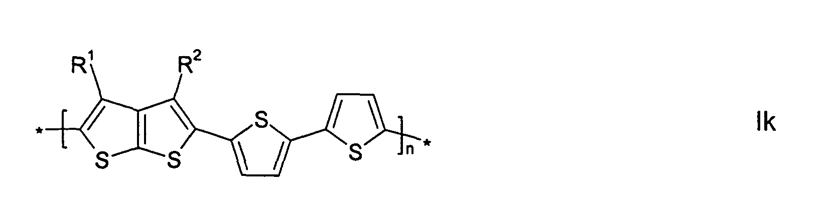


characterized in that they are selected of the following formulae


wherein at least one of the polymerisable mono-, oligo- and polymers of claims 1 to 9 and/or the further polymerisable compounds is mesogenic or liquid crystalline.
Priority Applications (1)
| Application Number | Priority Date | Filing Date | Title |
|---|---|---|---|
| EP04018079A EP1510535B1 (en) | 2003-08-28 | 2004-07-30 | Mono-, Oligo- and Polythieno(2,3-b)thiophenes |
Applications Claiming Priority (3)
| Application Number | Priority Date | Filing Date | Title |
|---|---|---|---|
| EP03019501 | 2003-08-28 | ||
| EP03019501 | 2003-08-28 | ||
| EP04018079A EP1510535B1 (en) | 2003-08-28 | 2004-07-30 | Mono-, Oligo- and Polythieno(2,3-b)thiophenes |
Publications (2)
| Publication Number | Publication Date |
|---|---|
| EP1510535A1 true EP1510535A1 (en) | 2005-03-02 |
| EP1510535B1 EP1510535B1 (en) | 2008-11-05 |
Family
ID=34400456
Family Applications (1)
| Application Number | Title | Priority Date | Filing Date |
|---|---|---|---|
| EP04018079A Expired - Lifetime EP1510535B1 (en) | 2003-08-28 | 2004-07-30 | Mono-, Oligo- and Polythieno(2,3-b)thiophenes |
Country Status (5)
| Country | Link |
|---|---|
| US (1) | US7183418B2 (en) |
| EP (1) | EP1510535B1 (en) |
| JP (2) | JP5301071B2 (en) |
| AT (1) | ATE413423T1 (en) |
| DE (1) | DE602004017550D1 (en) |
Cited By (21)
| Publication number | Priority date | Publication date | Assignee | Title |
|---|---|---|---|---|
| WO2005111045A1 (en) * | 2004-05-18 | 2005-11-24 | Merck Patent Gmbh | MONO-, OLIGO- AND POLYTHIENO[3,2-b]THIOPHENES |
| WO2005121150A1 (en) * | 2004-06-09 | 2005-12-22 | Merck Patent Gmbh | POLYMERISABLE THIENO[3,2-b]THIOPHENES |
| WO2006021277A1 (en) | 2004-08-21 | 2006-03-02 | Merck Patent Gmbh | MONOMERS, OLIGOMERS AND POLYMERS OF THIENO[2,3-b]THIOPHENE |
| WO2006031893A3 (en) * | 2004-09-14 | 2006-05-04 | Corning Inc | Fused thiophenes, methods for making fused thiophenes, and uses thereof |
| WO2007008977A1 (en) * | 2005-07-11 | 2007-01-18 | University Of Connecticut | Polymers of thieno[3,4-b]furan, method of making, and use thereof |
| EP1754736A1 (en) * | 2005-08-16 | 2007-02-21 | Merck Patent GmbH | Process for the polymerisation of thiophene or selenophene derivatives |
| EP1993105A1 (en) * | 2007-05-16 | 2008-11-19 | Samsung Electronics Co., Ltd. | Organic semiconductor polymer having liquid crystal properties, organic active layer, organic thin film transistor, and electronic device including the same, and methods of fabricating the same |
| WO2008106019A3 (en) * | 2007-02-28 | 2009-04-02 | Corning Inc | Fused thiophenes, methods for making fused thiophenes, and uses thereof |
| US20090326187A1 (en) * | 2008-06-26 | 2009-12-31 | Sotzing Gregory A | SYNTHESIS OF THIENO[3,4-b]THIOPHENE, THIENO[3,4-b]FURAN, RELATED COMPOUNDS AND THEIR DERIVATIVES AND USE THEREOF |
| US7746533B2 (en) | 2005-07-11 | 2010-06-29 | The University Of Connecticut | Electrochromic devices utilizing very low band gap conjugated counter electrodes: preparation and use |
| US7893191B2 (en) | 2007-02-28 | 2011-02-22 | Corning Incorporated | Fused thiophenes, methods for making fused thiophenes, and uses thereof |
| US7910684B2 (en) | 2007-09-06 | 2011-03-22 | Xerox Corporation | Diketopyrrolopyrrole-based derivatives for thin film transistors |
| US7919573B2 (en) | 2005-11-16 | 2011-04-05 | Xerox Corporation | Polymer having thieno[3,2-b] thiophene moieties |
| US7932344B2 (en) | 2007-09-06 | 2011-04-26 | Xerox Corporation | Diketopyrrolopyrrole-based polymers |
| WO2011067192A2 (en) | 2009-12-02 | 2011-06-09 | Basf Se | Dithienobenzo-thieno[3,2-b]thiophene-copolymer and its use as high performance solution processable semiconducting polymer |
| US8178629B2 (en) | 2005-01-31 | 2012-05-15 | University Of Connecticut | Conjugated polymer fiber, preparation and use thereof |
| US8227567B2 (en) | 2006-02-16 | 2012-07-24 | University Of Connecticut | Conductive polymers from precursor polymers, method of making, and use thereof |
| US8471064B2 (en) | 2006-07-21 | 2013-06-25 | Merck Patent Gmbh | Copolymers of indenofluorene and thiophene |
| US8501902B2 (en) | 2005-08-16 | 2013-08-06 | Merck Patent Gmbh | Process for the polymerisation of thiophene or selenophene compounds |
| CN102149750B (en) * | 2008-07-18 | 2014-04-23 | 芝加哥大学 | Semiconducting polymers |
| CN103848967A (en) * | 2012-11-28 | 2014-06-11 | 海洋王照明科技股份有限公司 | Polymer containing thienothiophene, benzothiadiazole and cyclopentadithiophene, preparation method and application thereof |
Families Citing this family (31)
| Publication number | Priority date | Publication date | Assignee | Title |
|---|---|---|---|---|
| US7569158B2 (en) * | 2004-10-13 | 2009-08-04 | Air Products And Chemicals, Inc. | Aqueous dispersions of polythienothiophenes with fluorinated ion exchange polymers as dopants |
| CN102321234A (en) * | 2005-05-24 | 2012-01-18 | 日立化成工业株式会社 | Process for producing conjugated polymer |
| JP2007088224A (en) * | 2005-09-22 | 2007-04-05 | Konica Minolta Holdings Inc | Organic semiconductor material and organic semiconductor film using same, organic semiconductor device, and organic thin-film transistor |
| DE602007007003D1 (en) * | 2006-03-24 | 2010-07-22 | Merck Patent Gmbh | Organic semiconductor formulation |
| TW201002722A (en) * | 2008-01-22 | 2010-01-16 | Ricoh Co Ltd | Benzobisthiazole compound, benzobisthiazole polymer, organic film including the compound or polymer and transistor including the organic film |
| US8367798B2 (en) * | 2008-09-29 | 2013-02-05 | The Regents Of The University Of California | Active materials for photoelectric devices and devices that use the materials |
| JP5245123B2 (en) * | 2008-10-09 | 2013-07-24 | コニカミノルタ株式会社 | Organic photoelectric conversion element, solar cell, and optical sensor array |
| US7872258B2 (en) * | 2008-11-19 | 2011-01-18 | Xerox Corporation | Organic thin-film transistors |
| US8372945B2 (en) | 2009-07-24 | 2013-02-12 | Solarmer Energy, Inc. | Conjugated polymers with carbonyl substituted thieno[3,4-B]thiophene units for polymer solar cell active layer materials |
| CN102276801B (en) * | 2010-06-10 | 2014-03-12 | 海洋王照明科技股份有限公司 | Thienothiophene quinoid organic photoelectric material as well as preparation method and application thereof |
| US8895693B2 (en) | 2010-06-25 | 2014-11-25 | Samsung Electronics Co., Ltd. | Electron-donating polymers and organic solar cells including the same |
| JP2012167057A (en) * | 2011-02-15 | 2012-09-06 | Sumitomo Chemical Co Ltd | Compound, method for producing the same, thin film comprising the compound, and organic transistor comprising the thin film |
| US9184315B2 (en) * | 2011-03-08 | 2015-11-10 | Nankai University | Photoelectric materials and preparation thereof |
| TW201302842A (en) * | 2011-03-31 | 2013-01-16 | Kuraray Co | Block copolymer and photoelectric conversion element |
| KR101545429B1 (en) | 2011-04-15 | 2015-08-18 | 더 유니버시티 오브 시카고 | Semiconducting polymers |
| EP2702086B1 (en) * | 2011-04-28 | 2015-03-18 | Basf Se | Semiconductor materials based on diketopiperidinopiperidine copolymers |
| KR101489617B1 (en) | 2011-04-28 | 2015-02-04 | 바스프 에스이 | Semiconductor materials based on thienothiophene-2,5-dione oligomers and polymers |
| JP5650051B2 (en) | 2011-05-09 | 2015-01-07 | Jx日鉱日石エネルギー株式会社 | Organic semiconductor |
| KR101853395B1 (en) | 2011-05-23 | 2018-04-30 | 삼성전자주식회사 | Electron donating polymer and solar cell including the same |
| KR101777326B1 (en) | 2011-10-05 | 2017-09-12 | 삼성전자주식회사 | Electron donating polymer and organic solar cell including the same |
| KR20140129080A (en) | 2012-02-03 | 2014-11-06 | 더 유니버시티 오브 시카고 | Semiconducting polymers |
| US8901543B2 (en) | 2012-02-15 | 2014-12-02 | Kyushu University National University Corporation | Organic semiconductor device and its production method, and compound |
| WO2014031282A1 (en) | 2012-08-23 | 2014-02-27 | Phillips 66 Company | Benzobisthiazole building blocks for conjugated polymers |
| JP6488616B2 (en) * | 2013-10-04 | 2019-03-27 | 日産化学株式会社 | Charge transporting thin film forming varnish, charge transporting thin film and organic electroluminescent device |
| US10115917B2 (en) * | 2015-05-19 | 2018-10-30 | Northwestern University | Dopant-free polymeric hole-transporting materials for perovskite solar cell |
| WO2017058406A1 (en) | 2015-10-01 | 2017-04-06 | Phillips 66 Company | Formation of films for organic photovoltaics |
| US9911919B2 (en) | 2015-10-01 | 2018-03-06 | Phillips 66 Company | Process of manufacturing an electron transport material |
| US10418555B2 (en) | 2015-10-01 | 2019-09-17 | Phillips 66 Company | Formation of films for organic photovoltaics |
| US10312448B2 (en) | 2015-10-01 | 2019-06-04 | Phillips 66 Company | Process of manufacturing an electron transport material |
| US9905769B2 (en) | 2015-10-01 | 2018-02-27 | Phillips 66 Company | Process of manufacturing an electron transport material |
| US10818849B2 (en) | 2015-12-29 | 2020-10-27 | The University Of Chicago | Electron acceptors based on alpha-position substituted PDI for OPV solar cells |
Citations (3)
| Publication number | Priority date | Publication date | Assignee | Title |
|---|---|---|---|---|
| EP0144013A2 (en) * | 1983-11-25 | 1985-06-12 | MERCK PATENT GmbH | Thienothiophene derivatives |
| EP1275651A2 (en) * | 2001-07-09 | 2003-01-15 | MERCK PATENT GmbH | Thienothiophene derivatives |
| EP1300430A1 (en) * | 2001-09-29 | 2003-04-09 | MERCK PATENT GmbH | Mono-, oligo- and polymers of benzo[b]thiophene and 2,2'-bisbenzo[b]thiophene and their use as charge transport materials |
Family Cites Families (10)
| Publication number | Priority date | Publication date | Assignee | Title |
|---|---|---|---|---|
| JPH0686457B2 (en) * | 1989-07-03 | 1994-11-02 | ダイソー株式会社 | Thiophene derivative, complex containing the same, and method for producing the same |
| DE4234230C2 (en) * | 1992-10-10 | 2003-08-14 | Covion Organic Semiconductors | Substituted thieno [3,2-b] thiophenes and their use |
| JPH07188399A (en) * | 1993-12-27 | 1995-07-25 | Unitika Ltd | Moldable or film-forming composition changing to be electrically conductive by light irradiation |
| US6130339A (en) * | 1999-06-01 | 2000-10-10 | The United States Of America As Represented By The Secretary Of The Air Force | Electro-active monomers comprised of aniline-thiophene units |
| JP4419309B2 (en) * | 2000-10-16 | 2010-02-24 | 宇部興産株式会社 | Nonaqueous electrolyte and lithium secondary battery using the same |
| KR100911136B1 (en) * | 2001-07-09 | 2009-08-06 | 메르크 파텐트 게엠베하 | Reactive thienothiophenes |
| ATE303389T1 (en) * | 2001-07-09 | 2005-09-15 | Merck Patent Gmbh | THIENOTHIOPHENE DERIVATIVES |
| ATE473251T1 (en) * | 2001-09-29 | 2010-07-15 | Merck Patent Gmbh | MONO-, OLIGO- AND POLYMERS OF BENZO(B)THIOPHENE AND 2,2'-BISBENZOTHIOPHENE AND THEIR USE AS CHARGE TRANSPORT MATERIAL |
| US7118692B2 (en) * | 2004-10-04 | 2006-10-10 | Air Products And Chemicals, Inc. | Substituted thienothiophene monomers and conducting polymers |
| JP4608853B2 (en) * | 2003-07-24 | 2011-01-12 | 三菱化学株式会社 | Hologram recording composition, thiophene ring compound, and hologram recording medium |
-
2004
- 2004-07-30 EP EP04018079A patent/EP1510535B1/en not_active Expired - Lifetime
- 2004-07-30 DE DE602004017550T patent/DE602004017550D1/en not_active Expired - Lifetime
- 2004-07-30 AT AT04018079T patent/ATE413423T1/en not_active IP Right Cessation
- 2004-08-30 US US10/928,724 patent/US7183418B2/en not_active Expired - Lifetime
- 2004-08-30 JP JP2004249474A patent/JP5301071B2/en not_active Expired - Fee Related
-
2012
- 2012-03-13 JP JP2012056062A patent/JP5301698B2/en not_active Expired - Fee Related
Patent Citations (3)
| Publication number | Priority date | Publication date | Assignee | Title |
|---|---|---|---|---|
| EP0144013A2 (en) * | 1983-11-25 | 1985-06-12 | MERCK PATENT GmbH | Thienothiophene derivatives |
| EP1275651A2 (en) * | 2001-07-09 | 2003-01-15 | MERCK PATENT GmbH | Thienothiophene derivatives |
| EP1300430A1 (en) * | 2001-09-29 | 2003-04-09 | MERCK PATENT GmbH | Mono-, oligo- and polymers of benzo[b]thiophene and 2,2'-bisbenzo[b]thiophene and their use as charge transport materials |
Non-Patent Citations (1)
| Title |
|---|
| KOSSMEHL,G.; BEIMLING,P.; MANECKE,G.: "Über Polyarylenalkenylene und Polyheteroarylenalkenylene, 12 Synthesen und Charakterisierung von Poly(thieno[2,3-b]thiophen-2,5-diylvinylenarylenvinylen)en, Poly(thieno[3,2-b]thiophen-2,5-diylvinylenarylenvinylen)en, und einigen Modellverbindungen", MAKROMOL. CHEM., vol. 183, 1982, pages 2747 - 2769, XP002305732 * |
Cited By (36)
| Publication number | Priority date | Publication date | Assignee | Title |
|---|---|---|---|---|
| WO2005111045A1 (en) * | 2004-05-18 | 2005-11-24 | Merck Patent Gmbh | MONO-, OLIGO- AND POLYTHIENO[3,2-b]THIOPHENES |
| US7714098B2 (en) | 2004-05-18 | 2010-05-11 | Merck Patent Gmbh | Mono-, oligo- and polythieno[3,2-b]thiophenes |
| WO2005121150A1 (en) * | 2004-06-09 | 2005-12-22 | Merck Patent Gmbh | POLYMERISABLE THIENO[3,2-b]THIOPHENES |
| US7700643B2 (en) | 2004-06-09 | 2010-04-20 | Merck Patent Gmbh | Polymerisable thieno[3,2-b]thiophenes |
| WO2006021277A1 (en) | 2004-08-21 | 2006-03-02 | Merck Patent Gmbh | MONOMERS, OLIGOMERS AND POLYMERS OF THIENO[2,3-b]THIOPHENE |
| US8114316B2 (en) | 2004-08-21 | 2012-02-14 | Merck Patent Gmbh | Monomers, oligomers and polymers of thieno[2,3-b]thiophene |
| US7838623B2 (en) | 2004-09-14 | 2010-11-23 | Corning Incorporated | Fused thiophenes, methods for making fused thiophenes, and uses thereof |
| WO2006031893A3 (en) * | 2004-09-14 | 2006-05-04 | Corning Inc | Fused thiophenes, methods for making fused thiophenes, and uses thereof |
| US8389669B2 (en) | 2004-09-14 | 2013-03-05 | Corning Incorporated | Fused thiophenes, methods for making fused thiophenes, and uses thereof |
| US8349998B2 (en) | 2004-09-14 | 2013-01-08 | Corning Incorporated | Fused thiophenes, methods for making fused thiophenes, and uses thereof |
| US7705108B2 (en) | 2004-09-14 | 2010-04-27 | Corning Incorporated | Fused thiophenes, methods for making fused thiophenes, and uses thereof |
| US8178629B2 (en) | 2005-01-31 | 2012-05-15 | University Of Connecticut | Conjugated polymer fiber, preparation and use thereof |
| WO2007008977A1 (en) * | 2005-07-11 | 2007-01-18 | University Of Connecticut | Polymers of thieno[3,4-b]furan, method of making, and use thereof |
| US7746533B2 (en) | 2005-07-11 | 2010-06-29 | The University Of Connecticut | Electrochromic devices utilizing very low band gap conjugated counter electrodes: preparation and use |
| US7737247B2 (en) | 2005-07-11 | 2010-06-15 | The University Of Connecticut | Polymers of thieno[3,4-b]furan, method of making, and use thereof |
| US8501902B2 (en) | 2005-08-16 | 2013-08-06 | Merck Patent Gmbh | Process for the polymerisation of thiophene or selenophene compounds |
| EP1754736A1 (en) * | 2005-08-16 | 2007-02-21 | Merck Patent GmbH | Process for the polymerisation of thiophene or selenophene derivatives |
| US7919574B2 (en) | 2005-11-16 | 2011-04-05 | Xerox Corporation | Polymer having thieno[3,2-b] thiophene moieties |
| TWI472550B (en) * | 2005-11-16 | 2015-02-11 | Xerox Corp | a polymer having a thieno[3,2-b]thiophene moiety |
| US7919573B2 (en) | 2005-11-16 | 2011-04-05 | Xerox Corporation | Polymer having thieno[3,2-b] thiophene moieties |
| US9127121B2 (en) | 2006-02-16 | 2015-09-08 | The University Of Connecticut | Conductive polymers from precursor polymers, method of making, and use thereof |
| US8227567B2 (en) | 2006-02-16 | 2012-07-24 | University Of Connecticut | Conductive polymers from precursor polymers, method of making, and use thereof |
| US8471064B2 (en) | 2006-07-21 | 2013-06-25 | Merck Patent Gmbh | Copolymers of indenofluorene and thiophene |
| WO2008106019A3 (en) * | 2007-02-28 | 2009-04-02 | Corning Inc | Fused thiophenes, methods for making fused thiophenes, and uses thereof |
| US7893191B2 (en) | 2007-02-28 | 2011-02-22 | Corning Incorporated | Fused thiophenes, methods for making fused thiophenes, and uses thereof |
| US8008426B2 (en) | 2007-05-16 | 2011-08-30 | Samsung Electronics Co., Ltd. | Organic semiconductor polymer having liquid crystal properties, organic active layer, organic thin film transistor, and electronic device including the same, and methods of fabricating the same |
| EP1993105A1 (en) * | 2007-05-16 | 2008-11-19 | Samsung Electronics Co., Ltd. | Organic semiconductor polymer having liquid crystal properties, organic active layer, organic thin film transistor, and electronic device including the same, and methods of fabricating the same |
| US7910684B2 (en) | 2007-09-06 | 2011-03-22 | Xerox Corporation | Diketopyrrolopyrrole-based derivatives for thin film transistors |
| US7932344B2 (en) | 2007-09-06 | 2011-04-26 | Xerox Corporation | Diketopyrrolopyrrole-based polymers |
| US20090326187A1 (en) * | 2008-06-26 | 2009-12-31 | Sotzing Gregory A | SYNTHESIS OF THIENO[3,4-b]THIOPHENE, THIENO[3,4-b]FURAN, RELATED COMPOUNDS AND THEIR DERIVATIVES AND USE THEREOF |
| US8168671B2 (en) | 2008-06-26 | 2012-05-01 | The University Of Connecticut | Synthesis of thieno[3,4-b]thiophene, thieno[3,4-b]furan, related compounds and their derivatives and use thereof |
| CN102149750B (en) * | 2008-07-18 | 2014-04-23 | 芝加哥大学 | Semiconducting polymers |
| US8389670B2 (en) | 2009-12-02 | 2013-03-05 | Basf Se | Dithienobenzo-thieno[3,2-B]thiophene-copolymer and its use as high performance solution processable semiconducting polymer |
| WO2011067192A2 (en) | 2009-12-02 | 2011-06-09 | Basf Se | Dithienobenzo-thieno[3,2-b]thiophene-copolymer and its use as high performance solution processable semiconducting polymer |
| CN103848967A (en) * | 2012-11-28 | 2014-06-11 | 海洋王照明科技股份有限公司 | Polymer containing thienothiophene, benzothiadiazole and cyclopentadithiophene, preparation method and application thereof |
| CN103848967B (en) * | 2012-11-28 | 2016-01-27 | 海洋王照明科技股份有限公司 | A kind of containing thienothiophene, diazosulfide and cyclopentano two thiophen polymer and preparation and application thereof |
Also Published As
| Publication number | Publication date |
|---|---|
| ATE413423T1 (en) | 2008-11-15 |
| JP5301698B2 (en) | 2013-09-25 |
| JP2012162720A (en) | 2012-08-30 |
| EP1510535B1 (en) | 2008-11-05 |
| DE602004017550D1 (en) | 2008-12-18 |
| JP5301071B2 (en) | 2013-09-25 |
| US7183418B2 (en) | 2007-02-27 |
| US20050090640A1 (en) | 2005-04-28 |
| JP2005076030A (en) | 2005-03-24 |
Similar Documents
| Publication | Publication Date | Title |
|---|---|---|
| EP1510535B1 (en) | Mono-, Oligo- and Polythieno(2,3-b)thiophenes | |
| US7524922B2 (en) | Poly(benzodithiophenes) | |
| US6676857B2 (en) | Mono-, oligo- and poly-4-fluorothiophenes and their use as charge transport materials | |
| US20040176560A1 (en) | Mono-, Oligo-and polymers comprising fluorene and aryl groups | |
| US7470377B2 (en) | Monomers, oligomers and polymers comprising thiophene and selenophene | |
| WO2005121150A1 (en) | POLYMERISABLE THIENO[3,2-b]THIOPHENES | |
| EP1279689B1 (en) | Mono-, Oligo and Poly-3-(1,1-difluoroalkyl)thiophenes and their use as charge transport materials | |
| US8114316B2 (en) | Monomers, oligomers and polymers of thieno[2,3-b]thiophene | |
| EP1524286B1 (en) | Poly(benzodithiophenes) | |
| EP1300430B1 (en) | Mono-, oligo- and polymers of benzo(b)thiophene and 2,2'-bisbenzo(b)thiophene and their use as charge transport materials | |
| EP1284258B1 (en) | Mono-, oligo- and polyalkylidenefluorenes and their use as charge transport materials | |
| EP1951787B1 (en) | Regioregular polyselenophenes | |
| EP1398336B1 (en) | Mono-, Oligo- and Poly(3-alkynylthiophenes) and their Use as Charge Transport Materials | |
| EP1279690A1 (en) | Mono-oligo- and poly-3-substituted-4-fluorothiophenes and their use as charge transport materials | |
| EP1439590A2 (en) | Mono-, oligo- and poly-bis(thienyl) arylenes and their use as charge transport materials | |
| EP1475401B1 (en) | Mono-, oligo- and polymers comprising fluorene and aryl groups | |
| WO2005080369A2 (en) | Reactive mesogenic charge transport compounds containing at least two thiophene groups | |
| EP1275652A2 (en) | Mono-, oligo- and polydithienopyridines and their use as charge transport materials |
Legal Events
| Date | Code | Title | Description |
|---|---|---|---|
| PUAI | Public reference made under article 153(3) epc to a published international application that has entered the european phase |
Free format text: ORIGINAL CODE: 0009012 |
|
| 17P | Request for examination filed |
Effective date: 20040730 |
|
| AK | Designated contracting states |
Kind code of ref document: A1 Designated state(s): AT BE BG CH CY CZ DE DK EE ES FI FR GB GR HU IE IT LI LU MC NL PL PT RO SE SI SK TR |
|
| AX | Request for extension of the european patent |
Extension state: AL HR LT LV MK |
|
| AKX | Designation fees paid |
Designated state(s): AT BE BG CH CY CZ DE DK EE ES FI FR GB GR HU IE IT LI LU MC NL PL PT RO SE SI SK TR |
|
| 17Q | First examination report despatched |
Effective date: 20060328 |
|
| GRAP | Despatch of communication of intention to grant a patent |
Free format text: ORIGINAL CODE: EPIDOSNIGR1 |
|
| GRAS | Grant fee paid |
Free format text: ORIGINAL CODE: EPIDOSNIGR3 |
|
| GRAA | (expected) grant |
Free format text: ORIGINAL CODE: 0009210 |
|
| AK | Designated contracting states |
Kind code of ref document: B1 Designated state(s): AT BE BG CH CY CZ DE DK EE ES FI FR GB GR HU IE IT LI LU MC NL PL PT RO SE SI SK TR |
|
| REG | Reference to a national code |
Ref country code: GB Ref legal event code: FG4D |
|
| REG | Reference to a national code |
Ref country code: CH Ref legal event code: EP |
|
| REG | Reference to a national code |
Ref country code: IE Ref legal event code: FG4D |
|
| REF | Corresponds to: |
Ref document number: 602004017550 Country of ref document: DE Date of ref document: 20081218 Kind code of ref document: P |
|
| PG25 | Lapsed in a contracting state [announced via postgrant information from national office to epo] |
Ref country code: AT Free format text: LAPSE BECAUSE OF FAILURE TO SUBMIT A TRANSLATION OF THE DESCRIPTION OR TO PAY THE FEE WITHIN THE PRESCRIBED TIME-LIMIT Effective date: 20081105 Ref country code: ES Free format text: LAPSE BECAUSE OF FAILURE TO SUBMIT A TRANSLATION OF THE DESCRIPTION OR TO PAY THE FEE WITHIN THE PRESCRIBED TIME-LIMIT Effective date: 20090216 |
|
| PG25 | Lapsed in a contracting state [announced via postgrant information from national office to epo] |
Ref country code: PL Free format text: LAPSE BECAUSE OF FAILURE TO SUBMIT A TRANSLATION OF THE DESCRIPTION OR TO PAY THE FEE WITHIN THE PRESCRIBED TIME-LIMIT Effective date: 20081105 Ref country code: FI Free format text: LAPSE BECAUSE OF FAILURE TO SUBMIT A TRANSLATION OF THE DESCRIPTION OR TO PAY THE FEE WITHIN THE PRESCRIBED TIME-LIMIT Effective date: 20081105 Ref country code: SI Free format text: LAPSE BECAUSE OF FAILURE TO SUBMIT A TRANSLATION OF THE DESCRIPTION OR TO PAY THE FEE WITHIN THE PRESCRIBED TIME-LIMIT Effective date: 20081105 |
|
| PG25 | Lapsed in a contracting state [announced via postgrant information from national office to epo] |
Ref country code: DK Free format text: LAPSE BECAUSE OF FAILURE TO SUBMIT A TRANSLATION OF THE DESCRIPTION OR TO PAY THE FEE WITHIN THE PRESCRIBED TIME-LIMIT Effective date: 20081105 Ref country code: RO Free format text: LAPSE BECAUSE OF FAILURE TO SUBMIT A TRANSLATION OF THE DESCRIPTION OR TO PAY THE FEE WITHIN THE PRESCRIBED TIME-LIMIT Effective date: 20081105 Ref country code: EE Free format text: LAPSE BECAUSE OF FAILURE TO SUBMIT A TRANSLATION OF THE DESCRIPTION OR TO PAY THE FEE WITHIN THE PRESCRIBED TIME-LIMIT Effective date: 20081105 Ref country code: BG Free format text: LAPSE BECAUSE OF FAILURE TO SUBMIT A TRANSLATION OF THE DESCRIPTION OR TO PAY THE FEE WITHIN THE PRESCRIBED TIME-LIMIT Effective date: 20090205 Ref country code: BE Free format text: LAPSE BECAUSE OF FAILURE TO SUBMIT A TRANSLATION OF THE DESCRIPTION OR TO PAY THE FEE WITHIN THE PRESCRIBED TIME-LIMIT Effective date: 20081105 |
|
| PG25 | Lapsed in a contracting state [announced via postgrant information from national office to epo] |
Ref country code: CZ Free format text: LAPSE BECAUSE OF FAILURE TO SUBMIT A TRANSLATION OF THE DESCRIPTION OR TO PAY THE FEE WITHIN THE PRESCRIBED TIME-LIMIT Effective date: 20081105 Ref country code: SE Free format text: LAPSE BECAUSE OF FAILURE TO SUBMIT A TRANSLATION OF THE DESCRIPTION OR TO PAY THE FEE WITHIN THE PRESCRIBED TIME-LIMIT Effective date: 20090205 Ref country code: PT Free format text: LAPSE BECAUSE OF FAILURE TO SUBMIT A TRANSLATION OF THE DESCRIPTION OR TO PAY THE FEE WITHIN THE PRESCRIBED TIME-LIMIT Effective date: 20090406 |
|
| PLBE | No opposition filed within time limit |
Free format text: ORIGINAL CODE: 0009261 |
|
| STAA | Information on the status of an ep patent application or granted ep patent |
Free format text: STATUS: NO OPPOSITION FILED WITHIN TIME LIMIT |
|
| PG25 | Lapsed in a contracting state [announced via postgrant information from national office to epo] |
Ref country code: SK Free format text: LAPSE BECAUSE OF FAILURE TO SUBMIT A TRANSLATION OF THE DESCRIPTION OR TO PAY THE FEE WITHIN THE PRESCRIBED TIME-LIMIT Effective date: 20081105 |
|
| 26N | No opposition filed |
Effective date: 20090806 |
|
| PG25 | Lapsed in a contracting state [announced via postgrant information from national office to epo] |
Ref country code: MC Free format text: LAPSE BECAUSE OF NON-PAYMENT OF DUE FEES Effective date: 20090731 |
|
| REG | Reference to a national code |
Ref country code: CH Ref legal event code: PL |
|
| REG | Reference to a national code |
Ref country code: FR Ref legal event code: ST Effective date: 20100331 |
|
| REG | Reference to a national code |
Ref country code: IE Ref legal event code: MM4A |
|
| PG25 | Lapsed in a contracting state [announced via postgrant information from national office to epo] |
Ref country code: LI Free format text: LAPSE BECAUSE OF NON-PAYMENT OF DUE FEES Effective date: 20090731 Ref country code: CH Free format text: LAPSE BECAUSE OF NON-PAYMENT OF DUE FEES Effective date: 20090731 Ref country code: FR Free format text: LAPSE BECAUSE OF NON-PAYMENT OF DUE FEES Effective date: 20090731 |
|
| PG25 | Lapsed in a contracting state [announced via postgrant information from national office to epo] |
Ref country code: IE Free format text: LAPSE BECAUSE OF NON-PAYMENT OF DUE FEES Effective date: 20090730 |
|
| PG25 | Lapsed in a contracting state [announced via postgrant information from national office to epo] |
Ref country code: GR Free format text: LAPSE BECAUSE OF FAILURE TO SUBMIT A TRANSLATION OF THE DESCRIPTION OR TO PAY THE FEE WITHIN THE PRESCRIBED TIME-LIMIT Effective date: 20090206 |
|
| PG25 | Lapsed in a contracting state [announced via postgrant information from national office to epo] |
Ref country code: IT Free format text: LAPSE BECAUSE OF FAILURE TO SUBMIT A TRANSLATION OF THE DESCRIPTION OR TO PAY THE FEE WITHIN THE PRESCRIBED TIME-LIMIT Effective date: 20081105 |
|
| PG25 | Lapsed in a contracting state [announced via postgrant information from national office to epo] |
Ref country code: LU Free format text: LAPSE BECAUSE OF NON-PAYMENT OF DUE FEES Effective date: 20090730 |
|
| PG25 | Lapsed in a contracting state [announced via postgrant information from national office to epo] |
Ref country code: HU Free format text: LAPSE BECAUSE OF FAILURE TO SUBMIT A TRANSLATION OF THE DESCRIPTION OR TO PAY THE FEE WITHIN THE PRESCRIBED TIME-LIMIT Effective date: 20090506 |
|
| PG25 | Lapsed in a contracting state [announced via postgrant information from national office to epo] |
Ref country code: TR Free format text: LAPSE BECAUSE OF FAILURE TO SUBMIT A TRANSLATION OF THE DESCRIPTION OR TO PAY THE FEE WITHIN THE PRESCRIBED TIME-LIMIT Effective date: 20081105 |
|
| PG25 | Lapsed in a contracting state [announced via postgrant information from national office to epo] |
Ref country code: CY Free format text: LAPSE BECAUSE OF FAILURE TO SUBMIT A TRANSLATION OF THE DESCRIPTION OR TO PAY THE FEE WITHIN THE PRESCRIBED TIME-LIMIT Effective date: 20081105 |
|
| PGFP | Annual fee paid to national office [announced via postgrant information from national office to epo] |
Ref country code: DE Payment date: 20140724 Year of fee payment: 11 Ref country code: NL Payment date: 20140610 Year of fee payment: 11 |
|
| PGFP | Annual fee paid to national office [announced via postgrant information from national office to epo] |
Ref country code: GB Payment date: 20140730 Year of fee payment: 11 |
|
| REG | Reference to a national code |
Ref country code: DE Ref legal event code: R119 Ref document number: 602004017550 Country of ref document: DE |
|
| GBPC | Gb: european patent ceased through non-payment of renewal fee |
Effective date: 20150730 |
|
| REG | Reference to a national code |
Ref country code: NL Ref legal event code: MM Effective date: 20150801 |
|
| PG25 | Lapsed in a contracting state [announced via postgrant information from national office to epo] |
Ref country code: DE Free format text: LAPSE BECAUSE OF NON-PAYMENT OF DUE FEES Effective date: 20160202 Ref country code: GB Free format text: LAPSE BECAUSE OF NON-PAYMENT OF DUE FEES Effective date: 20150730 |
|
| PG25 | Lapsed in a contracting state [announced via postgrant information from national office to epo] |
Ref country code: NL Free format text: LAPSE BECAUSE OF NON-PAYMENT OF DUE FEES Effective date: 20150801 |