EP1835621A1 - Counter with correction circuity - Google Patents
Counter with correction circuity Download PDFInfo
- Publication number
- EP1835621A1 EP1835621A1 EP07104178A EP07104178A EP1835621A1 EP 1835621 A1 EP1835621 A1 EP 1835621A1 EP 07104178 A EP07104178 A EP 07104178A EP 07104178 A EP07104178 A EP 07104178A EP 1835621 A1 EP1835621 A1 EP 1835621A1
- Authority
- EP
- European Patent Office
- Prior art keywords
- input signal
- reference time
- count value
- time period
- state
- Prior art date
- Legal status (The legal status is an assumption and is not a legal conclusion. Google has not performed a legal analysis and makes no representation as to the accuracy of the status listed.)
- Granted
Links
Images


Classifications
-
- H—ELECTRICITY
- H03—ELECTRONIC CIRCUITRY
- H03K—PULSE TECHNIQUE
- H03K21/00—Details of pulse counters or frequency dividers
- H03K21/40—Monitoring; Error detection; Preventing or correcting improper counter operation
- H03K21/406—Synchronisation of counters
Definitions
- the present invention relates to a counter for counting periods of an input signal during a reference period.
- the present invention relates to counter comprising additional circuitry for correcting a count value to provide improved precision.
- Counters are limited however in that they generally count either the rising or falling edges of an input signal, and when the start and end times of the reference period are not close to the relevant edge of the input signal, the count value will be inaccurate. There is thus an inherent inaccuracy in the count value which can be as high as nearly two counts of the counter.
- Figure 1 illustrates a known method of increasing the accuracy of the counter without increasing the reference time period. Such a method is described for example in " A digitally controlled PLL for SoC applications", T. Olsson and P. Nilsson, IEEE Solid-State Circuits, vol.39, no.5, pp.751-760, May 2004 .
- a circuit comprises two counters, a first counter 2 which counts rising edges of an input signal, and a second counter 4 which counts the falling edges of the input signal.
- the input signal is provided to each counter on an input line 6.
- the first and second counters 2, 4 are controlled to count the rising and falling edges respectively of the input signal during the reference time period.
- the output of each counter is provided to an adder 8 which adds the counts together to provide a combined count value on output line 10, which represents the number of half periods of the input signal.
- One disadvantage of the circuit of figure 1 is that two counters are required instead of one. In practise, to achieve a sufficiently accurate frequency estimation, thousands of periods of the input signal are counted, and therefore the counters are for example 12-bit or 15-bit counters, which require a relatively significant chip area. There is thus a need for a counter that provides improved accuracy over the single counter solution described above, without requiring a second counter and without increasing the reference time period.
- Embodiments of the present invention aim to at least partially address the above-mentioned needs.
- counting circuitry for providing a corrected count value based on the number of rising and falling edges of an input signal occurring during a reference time period, the counting circuitry comprising a counter arranged to provide a first count value based on the number of rising or falling edges of said input signal occurring during said reference time period; characterised in that said counting circuitry further comprises adjustment circuitry arranged to generate a corrected count value by determining the state of said input signal at the start time and end time of said reference time period, and adjusting said first count value if the state of said input signal at the start of said reference time period is different from the state of said input signal at the end of said reference time period.
- the adjustment circuitry is preferably arranged to add a value to said first count value when said input signal is at a first state at said start time and at a second state at said end time, and to subtract a value when said input signal is at said second state at said start time and at said first state at said end time.
- the adjustment circuitry preferably comprises multiplying means arranged to multiply said first count value by two, and adding means arranged to selectively add one and selectively subtract one from the result of said multiplication to generate said corrected count value.
- the counter is preferably arranged to count the falling edges of said input signal during said reference time period, and said adjustment circuitry is arranged to add one to the result of said multiplication when said input signal is low at said start time and high at said end time, and minus one from the result of said multiplication when said input signal is high at said start time and low at said end time.
- the counter is preferably arranged to count the rising edges of said input signal during said reference time period, and said adjustment means is arranged to add one to the result of said multiplication when said input signal is high at said start time and low at said end time, and minus one from the result of said multiplication when said input signal is low at said start time and high at said end time.
- the start and end times of said reference time period are preferably determined by edges of a reference time signal
- the adjustment circuitry preferably comprises first sampling means arranged to sample said reference time signal with falling edges of said input signal and output the result, second sampling means arranged to sample said reference time signal with rising edges of said input signal and output the result, and third sampling means arranged to sample the output of one of said first and second sampling means with the rising and falling edges of the output of the other one of said first and second sampling means, the generation of said corrected count value being based on the output of said third sampling means.
- a calibration circuit for calibrating a voltage controlled oscillator, the voltage controlled oscillator generating an output oscillating signal
- said calibration circuit comprising a frequency detector as described above for providing a count value based on the number of rising and falling edges of said output signal of said voltage controlled oscillator and comparing means for comparing said count value with a reference value and calibrating said voltage controlled oscillator based on said comparison.
- the voltage controlled oscillator is preferably calibrated by shifting its operating range.
- a mobile device comprising counting circuitry according to any of the embodiments described above.
- a method of providing a count value based on the number of rising and falling edges of an input signal occurring during a reference time period comprising providing a first count value based on counting the number of rising or falling edges of said input signal occurring during said reference time period; characterised in that said method further comprises determining the state of said input signal at the start time and end time of the reference time period, adjusting said first count value if the state of said input signal at the start of said reference time period is different from the state of said input signal at the end of said reference time period to generate a corrected count value, and outputting the corrected count value.
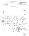
- FIG. 2 illustrates a counting circuit 20 according to one embodiment.
- This circuit allows the number of timing edges of an input signal during a reference time period t REF to be determined, and can be used for determining, for example, the frequency of the output of a voltage controlled oscillator (VCO).
- VCO voltage controlled oscillator
- the counting circuit 20 comprises a counter 22 having a reset input for resetting the count value of the counter.
- the counter is for example a 12-bit or 15-bit counter.
- the circuit further comprises adjustment circuitry 24 for detecting whether the count value from the counter should be adjusted. The outputs from the counter 22 and the adjustment circuitry 24 are provided to an adder block 26.
- the adjustment circuitry 24 receives a reference signal, t REF' on line 28, which represents a reference time period, and is preferably a clean signal generated by a quartz oscillator.
- the adjustment circuitry 24 also receives an input signal on line 30.
- the adjustment circuitry comprises first, second, third and fourth D-type flip-flops labelled 32, 34, 36 and 38 respectively, a two-input AND gate 48 and a two-input NOR gate 50.
- the signal t REF is provided on line 28 to the data input of each of the first and second flip-flop 32, 34.
- the input signal is provided on line 30 to the clock input of each of the first and second flip-flops, however it is inverted at the clock input of the first flip-flop 32, but not at the input of the second.
- the Q output of the first flip-flop 32 is connected to the clock inputs of the third and fourth flip-flops 36, 38, however it is inverted at the clock input of the third flip-flop but not at the input of the fourth.
- the inverse Q output of the second flip-flop 34 on line 42 is provided to the data input of the third and fourth flip-flops 36, 38. It is reminded that the Q output of a D-type flip-flop takes the value of the data input shortly after the significant edge (rising or falling) of the signal at its clock input.
- the inverse Q outputs from the third and fourth flip-flops on lines 44 and 46 respectively are each connected to one input of the AND gate 48 and one input of the NOR gate 50.
- the outputs of AND gate 48 on line 52 and of NOR gate 50 on line 54 are provided to an adder block 26, and in particular line 52 is connected to a '+1' input of the adder block 26, whilst line 54 is connected to a '-1' input of the adder block.
- Counter 22 receives a signal on line 58 from a two-input NAND gate 56.
- the first and second inputs of the NAND gate 56 are connected to the input signal on line 30 and to the Q output of the first flip-flop 32 on line 40 respectively.
- Counter 22 counts the rising edges of the signal on line 58 and provides the result on line 60 to the adder block 26, and in particular to a 'x2' input of the adder block.
- Adder block 26 provides an output count value on line 62, which comprises x+1 bits, where x is the number of bits of the counter.
- the output count value is determined as the count value on line 60 multiplied by two, and with one added or subtracted based on the signals on lines 52 and 54 respectively.
- each figure 3A to 3D illustrates signals at various points in the circuit of figure 2.
- each figure illustrates, with a corresponding reference numeral, the input signal on line 30, the reference timing signal t REF on line 28, the Q output of the first flip-flop on line 40, the inverse Q output of the second flip-flop on line 42, the inverse Q output of the third flip-flop on line 44, the inverse Q output of the fourth flip-flop on line 46, the output from AND gate 48 on line 52, the output from NOR gate 50 on line 54, the output from NAND gate 56 on line 58, the reset input to counter 22 and the count value on line 60.
- the reference time signal on line 28 comprises a rising edge 70 indicating the start of the reference time period t REF and a falling edge 72 indicating the end of this period.
- rising edge 70 occurs during a low half-period of the input signal on line 30, whilst falling edge 72 occurs during a high half-period of the input signal.
- Signal t REF is sampled at the first flip-flop by the falling edges of the input signal, and as shown the signal on line 40 goes high (edge 74) shortly after the falling edge 76 of input signal, and low (edge 78) shortly after the falling edge 80 of the input signal.
- Signal t REF is also sampled at the second flip-flop 34, but by the rising edges of the input signal.
- the signal on line 42 which is the inverse Q output, goes low (edge 82) shortly after the rising edge 84 of input signal, and high (edge 86) shortly after the rising edge 88 of the input signal.
- the inverse of the signal on line 40 is used to clock the output on line 42 of the second flip-flop, and as shown, the output signal on line 44, which is the inverse Q output, goes high (edge 90) shortly after the falling edge 78.
- This signal on line 44 indicates the state of the input signal at the end time (edge 72) of the reference time period, and therefore goes high indicating that the input signal was high.
- the signal on line 40 is used to clock the output on line 42 of the second flip-flop, and as shown, the output signal on line 46, which is the inverse Q output, goes high (edge 92) shortly after the falling edge 74.
- This signal on line 46 indicates the inverse of the state of the input signal at the start time (edge 70) of the reference time period, and therefore goes high indicating that the input signal was low.
- the signals on lines 44 and 46 are provided to AND gate 48 and NOR gate 50, which generate the signals indicating whether the count value should be adjusted by adding 1, subtracting 1, or if it should remain unchanged by doing neither.
- the signal on line 52 to the '+1' input of adder 26 is high, whilst the signal on line 54 to the '-1' input of the adder is low.
- the signal on line 58 is used to clock counter 22 during the reference time period.
- the signal on line 40 and the input signal on line 30 are connected to NAND gate 56 to generate the signal on line 58 that controls the counter 22.
- the two rising edges 90, 92 of this signal increment the count, which is shown rising from 0 to 2 on line 60.
- Line 60 and the output on the adder block on line 62 in fact comprise multiple data paths in parallel.
- the counter 22 is a 12-bit counter, and this line 60 comprises 12 parallel data paths, whilst line 62 comprises 13 parallel data paths.
- the count value relates to falling edges of the input signal.
- This count value is multiplied by two by the adder block 26, by shifting the binary signal one bit to the left, and adding a zero. For example, the binary count value "10" (2) becomes "100" (4). This provides an approximate value for the number of half periods of the input signal.
- Adder block 26 then adds one half period if the signal on line 52 is high, and subtracts one half period if the signal on line 54 is high. In the case of figure 3A, one half value is added, giving a total count of five, which is output on line 62.
- the reset signal resets the counter after the final count has been determined.
- the reset signal is for example controlled to go low a predetermined time after the end of the reference period (edge 72).
- the timing diagrams of figures 3B and 3C illustrates the cases in which the input signal is high or low respectively at both the start time and end time of the reference time period. In these cases nothing is added or subtracted from the count value, as indicated by both signals 52 and 54 being low in both cases. The count value therefore remains at four.
- the timing diagram of figure 3D illustrates the case in which the input signal is high at the start time and low at the end time of the reference period, and therefore the signal on line 54 is high, indicating that 1 is subtracted from the count value.
- the count value on line 62 can be provided to a variety of circuitry to perform a variety of functions.
- the counter circuitry can be used to calibrate the frequency of a voltage controlled oscillator, as will now be described with reference to figure 4.
- FIG 4 illustrates a calibration loop for calibrating a voltage controlled oscillator 100.
- VCO 100 receives an input control voltage V dc on line 102, this voltage controlling the oscillating frequency of the output signal of the VCO.
- the VCO also comprises a calibration input for receiving calibration signals on lines 104 for calibrating the VCO.
- VCO 100 comprises a number of switches (not shown in figure 4) for selecting the operating range of the VCO, in particular the maximum and minimum frequencies (f max and f min ) which correspond to maximum and minimum control voltage input levels. Whilst the magnitude of the operating range of the VCO (f max - f min ) remains constant, these switches allow the operating range to be shifted to calibrate the approximate frequency of the VCO output signal for a given input control voltage.
- the switches are set during a calibration phase such that, for example, the mid-frequency value required corresponds to a mid-voltage level of the supply voltage.
- the switches are controlled by signals provided at the calibration input on lines 104.
- the calibration circuit further comprises first and second counter blocks 106, 108, the output from each being connected to a comparator 110.
- the first counter block 106 receives a reference frequency signal f REF on line 112.
- the first counter block 106 counts the rising edges of f REF , and provides the output count value 'COUNT 1' on lines 114, this signal controlling states of the comparator 110.
- the first counter block also provides a timing signal on line 115 to the second counter block 108.
- the second counter block 108 is a counter block according to the circuit of figure 2 described above, and receives the timing signal from first counter block 106, which provides a reference time period t REF indicated by first and second edges.
- the reference time period is for example a half period of the signal f REF , or more preferably a number of periods of the input frequency signal f REF .
- the second counter block 108 also receives the output f OUT of the VCO 100 on line 116.
- the second counter block counts the rising or falling edges of the VCO output signal on line 116, and corrects the count value as described in relation to figure 2 above, before providing the output count value 'COUNT 2' on lines 118 to the comparator 110.
- Comparator 110 is a state machine that operates in one of a number of states determined by the signal 'COUNT 1' received from the first counter block 106. For example, the comparator is programmed to calibrate the VCO for 10 consecutive periods of f REF , and then to wait 300 periods before recalibrating. Comparator 110 receives a division ratio signal N DIV on lines 120 in the form of a word (for example 16 bits) indicating the required ratio between the reference frequency signal f REF and the frequency of the output signal of the VCO f OUT .
- a division ratio signal N DIV on lines 120 in the form of a word (for example 16 bits) indicating the required ratio between the reference frequency signal f REF and the frequency of the output signal of the VCO f OUT .
- the comparator 110 calibrates the switches of the VCO by providing signals on lines 104 such that the signal 'COUNT 2' on lines 118 is as close as possible to the division ratio signal N DIV , or to a multiple of n of N DIV in the case that t REF is equal to n half periods of the signal f REF .
- the output frequency signal of the VCO is calibrated such that: f OUT ⁇ N DIV ⁇ f REF
- the voltage level on line 102 is thus calibrated to be as close as possible to V dc .
- the present invention provides a counter circuit that provides a count value with improved precision based on rising and falling edges of an input signal without requiring two counters. This is achieved by counting rising or falling edges of the input signal during a reference time period, and determining whether this value needs to be adjusted by determining the state (high or low) of the input signal at the start time and end time of the reference period.
- the additional circuitry required to perform the task of determining this state of the input signal occupies much less chip space than the circuitry required by an additional counter.
- the extra precision of the counter is achieved without increasing the reference time period of the count, and therefore the result from the counter can be provided with no extra delay.
- the example of a calibration circuit for a VCO has been provided above, but embodiments of the counter circuit could also be used for other purposes such as to measure the gain of a VCO or as the divider in a digital phase locked loop.
- the counter circuitry described herein is particularly advantageous in environments in which area is limited, for example in mobile devices. In particular, the counter circuitry is useful in mobile devices for applications such as wireless local access networks (WLAN) and Bluetooth.
- WLAN wireless local access networks
- the inverse Q output has be used from the second, third and fourth flip-flops 34, 36, 38
- the standard Q output from each of these flip-flops could be used.
- a NAND gate 56 is used to generate the control signal to the counter 22, in alternative embodiments, different logic could be used.
- counter 22 could count the rising edges rather than the falling edges of the input signal, and the signal on lines 52 and 54 could be switched such that they are provided to the '-1' and '+1' inputs of the adder block 26 respectively, to provide the same result.
- the input signal is a symmetrical square-wave, in other words the rising and falling edges are equally spaced apart
- the spacing could be asymmetrical, and could for example have a known ratio between the length of the high and low pulses. In this case, the multiplication of the count value on line 60 and the values added or subtracted from this value could be adjusted accordingly.
Landscapes
- Stabilization Of Oscillater, Synchronisation, Frequency Synthesizers (AREA)
- Manipulation Of Pulses (AREA)
Abstract
Description
- The present invention relates to a counter for counting periods of an input signal during a reference period. In particular the present invention relates to counter comprising additional circuitry for correcting a count value to provide improved precision.
- In order to measure the frequency of an input oscillating signal, for example the square-wave output of a voltage controlled oscillator (VCO), a counter can be used. During a known reference time period, generally provided by a high quality quartz oscillator that generates clean timing edges, a counter counts the number of periods of the input oscillating signal. The frequency f can then be determined as:

where "count" is the count value reached by the counter during the reference period and tREF is the duration of the reference time period. - Counters are limited however in that they generally count either the rising or falling edges of an input signal, and when the start and end times of the reference period are not close to the relevant edge of the input signal, the count value will be inaccurate. There is thus an inherent inaccuracy in the count value which can be as high as nearly two counts of the counter. The frequency f of the input signal is thus:

where ε is the count error with 0<ε<2. - One way of reducing the effect of this error is to increase the reference time period so that the count is higher and the error ε becomes less significant. However according to this solution the time needed to calculate the input frequency is increased, and this is not compatible for applications in which a result from the counter is required quickly.
- Figure 1 illustrates a known method of increasing the accuracy of the counter without increasing the reference time period. Such a method is described for example in "A digitally controlled PLL for SoC applications", T. Olsson and P. Nilsson, IEEE Solid-State Circuits, vol.39, no.5, pp.751-760, May 2004.
- As shown in figure 1, a circuit comprises two counters, a
first counter 2 which counts rising edges of an input signal, and asecond counter 4 which counts the falling edges of the input signal. The input signal is provided to each counter on aninput line 6. The first andsecond counters adder 8 which adds the counts together to provide a combined count value onoutput line 10, which represents the number of half periods of the input signal. The error ε is therefore halved, and the frequency can be determined as:
- One disadvantage of the circuit of figure 1 is that two counters are required instead of one. In practise, to achieve a sufficiently accurate frequency estimation, thousands of periods of the input signal are counted, and therefore the counters are for example 12-bit or 15-bit counters, which require a relatively significant chip area. There is thus a need for a counter that provides improved accuracy over the single counter solution described above, without requiring a second counter and without increasing the reference time period.
- Embodiments of the present invention aim to at least partially address the above-mentioned needs.
- According to one aspect of the present invention, there is provided counting circuitry for providing a corrected count value based on the number of rising and falling edges of an input signal occurring during a reference time period, the counting circuitry comprising a counter arranged to provide a first count value based on the number of rising or falling edges of said input signal occurring during said reference time period; characterised in that said counting circuitry further comprises adjustment circuitry arranged to generate a corrected count value by determining the state of said input signal at the start time and end time of said reference time period, and adjusting said first count value if the state of said input signal at the start of said reference time period is different from the state of said input signal at the end of said reference time period.
- The adjustment circuitry is preferably arranged to add a value to said first count value when said input signal is at a first state at said start time and at a second state at said end time, and to subtract a value when said input signal is at said second state at said start time and at said first state at said end time.
- The adjustment circuitry preferably comprises multiplying means arranged to multiply said first count value by two, and adding means arranged to selectively add one and selectively subtract one from the result of said multiplication to generate said corrected count value.
- The counter is preferably arranged to count the falling edges of said input signal during said reference time period, and said adjustment circuitry is arranged to add one to the result of said multiplication when said input signal is low at said start time and high at said end time, and minus one from the result of said multiplication when said input signal is high at said start time and low at said end time.
- The counter is preferably arranged to count the rising edges of said input signal during said reference time period, and said adjustment means is arranged to add one to the result of said multiplication when said input signal is high at said start time and low at said end time, and minus one from the result of said multiplication when said input signal is low at said start time and high at said end time.
- The start and end times of said reference time period are preferably determined by edges of a reference time signal, and the adjustment circuitry preferably comprises first sampling means arranged to sample said reference time signal with falling edges of said input signal and output the result, second sampling means arranged to sample said reference time signal with rising edges of said input signal and output the result, and third sampling means arranged to sample the output of one of said first and second sampling means with the rising and falling edges of the output of the other one of said first and second sampling means, the generation of said corrected count value being based on the output of said third sampling means.
- According to a further aspect of the present invention, there is provided a calibration circuit for calibrating a voltage controlled oscillator, the voltage controlled oscillator generating an output oscillating signal, said calibration circuit comprising a frequency detector as described above for providing a count value based on the number of rising and falling edges of said output signal of said voltage controlled oscillator and comparing means for comparing said count value with a reference value and calibrating said voltage controlled oscillator based on said comparison.
- The voltage controlled oscillator is preferably calibrated by shifting its operating range.
- According to a further aspect of the present invention, a mobile device is provided comprising counting circuitry according to any of the embodiments described above.
- According to a further aspect of the present invention there is provided a method of providing a count value based on the number of rising and falling edges of an input signal occurring during a reference time period, the method comprising providing a first count value based on counting the number of rising or falling edges of said input signal occurring during said reference time period; characterised in that said method further comprises determining the state of said input signal at the start time and end time of the reference time period, adjusting said first count value if the state of said input signal at the start of said reference time period is different from the state of said input signal at the end of said reference time period to generate a corrected count value, and outputting the corrected count value.
- The foregoing and other purposes, features, aspects and advantages of the invention will become apparent from the following detailed description of a number of embodiments which is given by way of illustration only without limiting the invention, and throughout which reference is made to the accompanying drawings in which:
- figure 1 (already described above) illustrates a known counting circuit having two counters;
- figure 2 illustrates a counting circuit according to one embodiment of the present invention;
- figures 3A to 3D show timing diagrams for different states of the circuit of figure 2; and
- figure 4 illustrates an embodiment of a calibration circuit comprising counter circuits according to figure 2.
- Figure 2 illustrates a counting
circuit 20 according to one embodiment. This circuit allows the number of timing edges of an input signal during a reference time period tREF to be determined, and can be used for determining, for example, the frequency of the output of a voltage controlled oscillator (VCO). - The
counting circuit 20 comprises acounter 22 having a reset input for resetting the count value of the counter. The counter is for example a 12-bit or 15-bit counter. The circuit further comprisesadjustment circuitry 24 for detecting whether the count value from the counter should be adjusted. The outputs from thecounter 22 and theadjustment circuitry 24 are provided to anadder block 26. - The
adjustment circuitry 24 receives a reference signal, tREF' online 28, which represents a reference time period, and is preferably a clean signal generated by a quartz oscillator. Theadjustment circuitry 24 also receives an input signal online 30. - The adjustment circuitry comprises first, second, third and fourth D-type flip-flops labelled 32, 34, 36 and 38 respectively, a two-input AND
gate 48 and a two-input NOR gate 50. The signal tREF is provided online 28 to the data input of each of the first and second flip-flop line 30 to the clock input of each of the first and second flip-flops, however it is inverted at the clock input of the first flip-flop 32, but not at the input of the second. - The Q output of the first flip-
flop 32 is connected to the clock inputs of the third and fourth flip-flops flop 34 online 42 is provided to the data input of the third and fourth flip-flops - The inverse Q outputs from the third and fourth flip-flops on
lines AND gate 48 and one input of theNOR gate 50. The outputs ofAND gate 48 online 52 and ofNOR gate 50 online 54 are provided to anadder block 26, and inparticular line 52 is connected to a '+1' input of theadder block 26, whilstline 54 is connected to a '-1' input of the adder block. -
Counter 22 receives a signal online 58 from a two-input NAND gate 56. The first and second inputs of theNAND gate 56 are connected to the input signal online 30 and to the Q output of the first flip-flop 32 online 40 respectively.Counter 22 counts the rising edges of the signal online 58 and provides the result online 60 to theadder block 26, and in particular to a 'x2' input of the adder block. -
Adder block 26 provides an output count value online 62, which comprises x+1 bits, where x is the number of bits of the counter. The output count value is determined as the count value online 60 multiplied by two, and with one added or subtracted based on the signals onlines - Operation of the counting
circuit 20 of figure 2 will now be described with reference to the timing diagrams of figures 3A to 3D. - Each figure 3A to 3D illustrates signals at various points in the circuit of figure 2. In particular, each figure illustrates, with a corresponding reference numeral, the input signal on
line 30, the reference timing signal tREF online 28, the Q output of the first flip-flop online 40, the inverse Q output of the second flip-flop online 42, the inverse Q output of the third flip-flop online 44, the inverse Q output of the fourth flip-flop online 46, the output from ANDgate 48 online 52, the output from NORgate 50 online 54, the output fromNAND gate 56 online 58, the reset input to counter 22 and the count value online 60. - With reference to figure 3A, the reference time signal on
line 28 comprises a risingedge 70 indicating the start of the reference time period tREF and a fallingedge 72 indicating the end of this period. In thisexample rising edge 70 occurs during a low half-period of the input signal online 30, whilst fallingedge 72 occurs during a high half-period of the input signal. Signal tREF is sampled at the first flip-flop by the falling edges of the input signal, and as shown the signal online 40 goes high (edge 74) shortly after the fallingedge 76 of input signal, and low (edge 78) shortly after the fallingedge 80 of the input signal. Signal tREF is also sampled at the second flip-flop 34, but by the rising edges of the input signal. The signal online 42, which is the inverse Q output, goes low (edge 82) shortly after the risingedge 84 of input signal, and high (edge 86) shortly after the risingedge 88 of the input signal. - Next, at the third flip-
flop 36, the inverse of the signal online 40 is used to clock the output online 42 of the second flip-flop, and as shown, the output signal online 44, which is the inverse Q output, goes high (edge 90) shortly after the fallingedge 78. This signal online 44 indicates the state of the input signal at the end time (edge 72) of the reference time period, and therefore goes high indicating that the input signal was high. - At the fourth flip-
flop 38, the signal online 40 is used to clock the output online 42 of the second flip-flop, and as shown, the output signal online 46, which is the inverse Q output, goes high (edge 92) shortly after the falling edge 74. This signal online 46 indicates the inverse of the state of the input signal at the start time (edge 70) of the reference time period, and therefore goes high indicating that the input signal was low. - The signals on
lines gate 48 and NORgate 50, which generate the signals indicating whether the count value should be adjusted by adding 1, subtracting 1, or if it should remain unchanged by doing neither. As shown in figure 3A, the signal online 52 to the '+1' input ofadder 26 is high, whilst the signal online 54 to the '-1' input of the adder is low. - The signal on
line 58 is used to clock counter 22 during the reference time period. To ensure a clean signal to the counter, the signal online 40 and the input signal online 30 are connected toNAND gate 56 to generate the signal online 58 that controls thecounter 22. The two risingedges line 60.Line 60 and the output on the adder block online 62 in fact comprise multiple data paths in parallel. In the present example thecounter 22 is a 12-bit counter, and thisline 60 comprises 12 parallel data paths, whilstline 62 comprises 13 parallel data paths. - Due to the use of
NAND gate 56, the count value relates to falling edges of the input signal. This count value is multiplied by two by theadder block 26, by shifting the binary signal one bit to the left, and adding a zero. For example, the binary count value "10" (2) becomes "100" (4). This provides an approximate value for the number of half periods of the input signal.Adder block 26 then adds one half period if the signal online 52 is high, and subtracts one half period if the signal online 54 is high. In the case of figure 3A, one half value is added, giving a total count of five, which is output online 62. - The reset signal resets the counter after the final count has been determined. The reset signal is for example controlled to go low a predetermined time after the end of the reference period (edge 72).
- As a general rule, when the state (high or low) of the input signal at the start time of the reference period and at the end time of the reference period are the same, (both high or both low), no adjustment is required. In the embodiment of figure 2, in which the count is performed based on falling edges of the input signal, when the input signal is low at the start time and high at the end time of the reference period, one is added to the count value. On the other hand, if the input signal is high at the start time and low at the end time of the reference period, one is subtracted from the count value.
- The timing diagrams of figures 3B and 3C illustrates the cases in which the input signal is high or low respectively at both the start time and end time of the reference time period. In these cases nothing is added or subtracted from the count value, as indicated by both
signals - The timing diagram of figure 3D illustrates the case in which the input signal is high at the start time and low at the end time of the reference period, and therefore the signal on
line 54 is high, indicating that 1 is subtracted from the count value. The count value is therefore determined as 4-1=3. - The count value on
line 62 can be provided to a variety of circuitry to perform a variety of functions. - For example, the counter circuitry can be used to calibrate the frequency of a voltage controlled oscillator, as will now be described with reference to figure 4.
- Figure 4 illustrates a calibration loop for calibrating a voltage controlled
oscillator 100.VCO 100 receives an input control voltage Vdc online 102, this voltage controlling the oscillating frequency of the output signal of the VCO. The VCO also comprises a calibration input for receiving calibration signals onlines 104 for calibrating the VCO.VCO 100 comprises a number of switches (not shown in figure 4) for selecting the operating range of the VCO, in particular the maximum and minimum frequencies (fmax and fmin) which correspond to maximum and minimum control voltage input levels. Whilst the magnitude of the operating range of the VCO (fmax - fmin) remains constant, these switches allow the operating range to be shifted to calibrate the approximate frequency of the VCO output signal for a given input control voltage. The switches are set during a calibration phase such that, for example, the mid-frequency value required corresponds to a mid-voltage level of the supply voltage. The switches are controlled by signals provided at the calibration input onlines 104. - The calibration circuit further comprises first and second counter blocks 106, 108, the output from each being connected to a
comparator 110. Thefirst counter block 106 receives a reference frequency signal fREF online 112. The first counter block 106 counts the rising edges of fREF, and provides the output count value 'COUNT 1' onlines 114, this signal controlling states of thecomparator 110. The first counter block also provides a timing signal online 115 to thesecond counter block 108. - The
second counter block 108 is a counter block according to the circuit of figure 2 described above, and receives the timing signal fromfirst counter block 106, which provides a reference time period tREF indicated by first and second edges. The reference time period is for example a half period of the signal fREF, or more preferably a number of periods of the input frequency signal fREF. Thesecond counter block 108 also receives the output fOUT of theVCO 100 online 116. During the reference time period tREF the second counter block counts the rising or falling edges of the VCO output signal online 116, and corrects the count value as described in relation to figure 2 above, before providing the output count value 'COUNT 2' onlines 118 to thecomparator 110. -
Comparator 110 is a state machine that operates in one of a number of states determined by the signal 'COUNT 1' received from thefirst counter block 106. For example, the comparator is programmed to calibrate the VCO for 10 consecutive periods of fREF, and then to wait 300 periods before recalibrating.Comparator 110 receives a division ratio signal NDIV onlines 120 in the form of a word (for example 16 bits) indicating the required ratio between the reference frequency signal fREF and the frequency of the output signal of the VCO fOUT. During calibration periods of the reference frequency signal fREF thecomparator 110 calibrates the switches of the VCO by providing signals onlines 104 such that the signal 'COUNT 2' onlines 118 is as close as possible to the division ratio signal NDIV, or to a multiple of n of NDIV in the case that tREF is equal to n half periods of the signal fREF. Thus the output frequency signal of the VCO is calibrated such that:
- Once calibration is completed the control signals to the VCO on
lines 104 are fixed. A phase locked loop (not shown in figure 4) is then used to adjust the voltage level online 102 until the output frequency fOUT is the required frequency, such that:
- The voltage level on
line 102 is thus calibrated to be as close as possible to Vdc. - Thus the present invention provides a counter circuit that provides a count value with improved precision based on rising and falling edges of an input signal without requiring two counters. This is achieved by counting rising or falling edges of the input signal during a reference time period, and determining whether this value needs to be adjusted by determining the state (high or low) of the input signal at the start time and end time of the reference period. The additional circuitry required to perform the task of determining this state of the input signal occupies much less chip space than the circuitry required by an additional counter. Furthermore, the extra precision of the counter is achieved without increasing the reference time period of the count, and therefore the result from the counter can be provided with no extra delay.
- The example of a calibration circuit for a VCO has been provided above, but embodiments of the counter circuit could also be used for other purposes such as to measure the gain of a VCO or as the divider in a digital phase locked loop. The counter circuitry described herein is particularly advantageous in environments in which area is limited, for example in mobile devices. In particular, the counter circuitry is useful in mobile devices for applications such as wireless local access networks (WLAN) and Bluetooth.
- Whilst one embodiment of a
counter circuit 20 according to the invention has been described in detail with reference to figure 2, it will be apparent that there are many variations or alternatives that could be applied to this circuit. - For example, whilst the inverse Q output has be used from the second, third and fourth flip-
flops NAND gate 56 is used to generate the control signal to thecounter 22, in alternative embodiments, different logic could be used. - In alternative embodiments, counter 22 could count the rising edges rather than the falling edges of the input signal, and the signal on
lines adder block 26 respectively, to provide the same result. - Furthermore, whilst in the described embodiment the input signal is a symmetrical square-wave, in other words the rising and falling edges are equally spaced apart, in other embodiments, the spacing could be asymmetrical, and could for example have a known ratio between the length of the high and low pulses. In this case, the multiplication of the count value on
line 60 and the values added or subtracted from this value could be adjusted accordingly. - Whilst the example of a 13-bit count value at the
output 62 of the count circuit has been given above, the count value will be determined by the requirements of the circuit.
Claims (10)
- Counting circuitry for providing a corrected count value based on the number of rising and falling edges of an input signal occurring during a reference time period, the counting circuitry comprising:a counter (22) arranged to provide a first count value based on one of:characterised in that said counting circuitry further comprises adjustment circuitry (24-26) arranged to generate a corrected count value by determining the state of said input signal at the start time (70) and end time (72) of said reference time period, and adjusting said first count value if the state of said input signal at the start of said reference time period is different from the state of said input signal at the end of said reference time period.the number of said rising edges of said input signal occurring during said reference time period; andthe number of said falling edges of said input signal occurring during said reference time period;
- The counting circuitry of claim 1, wherein said adjustment circuitry is arranged to add a value to said first count value when said input signal is at a first state at said start time and at a second state at said end time, and to subtract a value when said input signal is at said second state at said start time and at said first state at said end time.
- The counting circuitry of claim 1 or 2, wherein said adjustment circuitry comprises multiplying means arranged to multiply said first count value by two, and adding means arranged to selectively add one and selectively subtract one from the result of said multiplication to generate said corrected count value.
- The counting circuitry of any preceding claim, wherein said counter (22) is arranged to count the falling edges of said input signal during said reference time period, and said adjustment circuitry is arranged to add one to the result of said multiplication when said input signal is low at said start time and high at said end time, and minus one from the result of said multiplication when said input signal is high at said start time and low at said end time.
- The counting circuitry of claim 3, wherein said counter (22) is arranged to count the rising edges of said input signal during said reference time period, and said adjustment means is arranged to add one to the result of said multiplication when said input signal is high at said start time and low at said end time, and minus one from the result of said multiplication when said input signal is low at said start time and high at said end time.
- The counting circuitry of any preceding claim, wherein said start and end times of said reference time period are determined by edges (70, 72) of a reference time signal, and said adjustment circuitry comprises:first sampling means (32) arranged to sample said reference time signal with falling edges of said input signal and output the result;second sampling means (34) arranged to sample said reference time signal with rising edges of said input signal and output the result; andthird sampling means (36, 38) arranged to sample the output of one of said first and second sampling means with the rising and falling edges of the output of the other one of said first and second sampling means, the generation of said corrected count value being based on the output of said third sampling means.
- A calibration circuit for calibrating a voltage controlled oscillator (100), the voltage controlled oscillator generating an output oscillating signal, said calibration circuit comprising:counting circuitry (106) according to claim 1, for providing a count value based on the number of rising and falling edges of said output signal of the voltage controlled oscillator (100); anda comparator for comparing said count value with a reference value and calibrating said voltage controlled oscillator based on said comparison.
- The calibration circuit of claim 7, wherein said voltage controlled oscillator is calibrated by shifting its operating range.
- A mobile device comprising counting circuitry for providing a corrected count value based on the number of rising and falling edges of an input signal occurring during a reference time period, the counting circuitry comprising:a counter (22) arranged to provide a first count value based on one of:characterised in that said counting circuitry further comprises adjustment circuitry (24-26) arranged to generate a corrected count value by determining the state of said input signal at the start time (70) and end time (72) of said reference time period, and adjusting said first count value if the state of said input signal at the start of said reference time period is different from the state of said input signal at the end of said reference time period.the number of said rising edges of said input signal occurring during said reference time period; andthe number of said falling edges of said input signal occurring during said reference time period;
- A method of providing a count value based on the number of rising and falling edges of an input signal occurring during a reference time period, the method comprising:providing a first count value based on counting one of:characterised in that said method further comprises:the number of said rising edges of said input signal occurring during said reference time period; andthe number of said falling edges of said input signal occurring during said reference time period;determining the state of said input signal at the start time (70) and end time (72) of said reference time period;adjusting said first count value if the state of said input signal at the start of said reference time period is different from the state of said input signal at the end of said reference time period to generate a corrected count value; andoutputting the corrected count value.
Applications Claiming Priority (1)
| Application Number | Priority Date | Filing Date | Title |
|---|---|---|---|
| FR0650872A FR2898743A1 (en) | 2006-03-15 | 2006-03-15 | COUNTER WITH CORRECTION CIRCUIT |
Publications (2)
| Publication Number | Publication Date |
|---|---|
| EP1835621A1 true EP1835621A1 (en) | 2007-09-19 |
| EP1835621B1 EP1835621B1 (en) | 2010-09-01 |
Family
ID=37719385
Family Applications (1)
| Application Number | Title | Priority Date | Filing Date |
|---|---|---|---|
| EP07104178A Not-in-force EP1835621B1 (en) | 2006-03-15 | 2007-03-14 | Counter with correction circuity |
Country Status (4)
| Country | Link |
|---|---|
| US (1) | US7466789B2 (en) |
| EP (1) | EP1835621B1 (en) |
| DE (1) | DE602007008779D1 (en) |
| FR (1) | FR2898743A1 (en) |
Cited By (1)
| Publication number | Priority date | Publication date | Assignee | Title |
|---|---|---|---|---|
| EP3171183A1 (en) * | 2015-11-19 | 2017-05-24 | STmicroelectronics SA | Method and device for measuring the frequency of a signal |
Families Citing this family (12)
| Publication number | Priority date | Publication date | Assignee | Title |
|---|---|---|---|---|
| US7551109B1 (en) * | 2007-03-14 | 2009-06-23 | Ashmore Jr Benjamin H | Method, system and apparatus for dual mode operation of a converter |
| JP2008292325A (en) * | 2007-05-24 | 2008-12-04 | Sanyo Electric Co Ltd | Signal detection circuit |
| US8095102B2 (en) | 2008-11-17 | 2012-01-10 | Infineon Technologies Ag | Phase-lock loop |
| JP2010271091A (en) | 2009-05-20 | 2010-12-02 | Seiko Epson Corp | Frequency measuring device |
| JP5440999B2 (en) | 2009-05-22 | 2014-03-12 | セイコーエプソン株式会社 | Frequency measuring device |
| JP5517033B2 (en) * | 2009-05-22 | 2014-06-11 | セイコーエプソン株式会社 | Frequency measuring device |
| JP5582447B2 (en) | 2009-08-27 | 2014-09-03 | セイコーエプソン株式会社 | Electric circuit, sensor system including the electric circuit, and sensor device including the electric circuit |
| JP5815918B2 (en) | 2009-10-06 | 2015-11-17 | セイコーエプソン株式会社 | Frequency measuring method, frequency measuring apparatus, and apparatus provided with frequency measuring apparatus |
| JP5876975B2 (en) | 2009-10-08 | 2016-03-02 | セイコーエプソン株式会社 | Frequency measuring device and method of generating shift frequency division signal in frequency measuring device |
| JP5883558B2 (en) | 2010-08-31 | 2016-03-15 | セイコーエプソン株式会社 | Frequency measuring device and electronic device |
| CN112255553B (en) * | 2020-09-18 | 2024-03-05 | 北京汽车股份有限公司 | Chip for detecting decay of battery molecules, battery activity protection system and method |
| CN113162608B (en) * | 2021-05-19 | 2023-08-22 | 湖南国科微电子股份有限公司 | Compensation circuit applied to logic chip and time sequence compensation method |
Citations (3)
| Publication number | Priority date | Publication date | Assignee | Title |
|---|---|---|---|---|
| JPH11355110A (en) * | 1998-06-10 | 1999-12-24 | Oki Electric Ind Co Ltd | Clock abnormality detection circuit |
| US20040008060A1 (en) * | 2002-07-01 | 2004-01-15 | Fujitsu Limited | Clock multiplication circuit |
| US6861881B1 (en) * | 2003-09-29 | 2005-03-01 | National Semiconductor Corporation | Fractional clock divider using digital techniques |
Family Cites Families (8)
| Publication number | Priority date | Publication date | Assignee | Title |
|---|---|---|---|---|
| JPS63226115A (en) * | 1987-03-16 | 1988-09-20 | Fujitsu Ltd | Zero cross counter |
| US5056123A (en) * | 1989-11-03 | 1991-10-08 | Sundstrand Corporation | Frequency counter with round off function |
| US5440252A (en) * | 1993-09-13 | 1995-08-08 | Acer Peripherals, Inc. | State machine with hysteresis for detecting frequency of an input signal |
| US5896049A (en) * | 1997-10-21 | 1999-04-20 | Kohler Co. | Electrical signal frequency detector |
| DE19946092A1 (en) * | 1999-09-25 | 2001-03-29 | Philips Corp Intellectual Pty | Method and device for determining a 3D image data record of a periodically moving body organ |
| US6597205B2 (en) * | 2001-12-21 | 2003-07-22 | Honeywell International Inc. | High accuracy method for determining the frequency of a pulse input signal over a wide frequency range |
| DE10355275B4 (en) * | 2003-11-26 | 2009-03-05 | Siemens Ag | catheter device |
| DE102004020587B4 (en) * | 2004-04-27 | 2016-02-18 | Siemens Aktiengesellschaft | Method and apparatus for visually assisting a catheter electrophysiology application with 2D fluoroscopic images |
-
2006
- 2006-03-15 FR FR0650872A patent/FR2898743A1/en not_active Withdrawn
-
2007
- 2007-03-14 DE DE602007008779T patent/DE602007008779D1/en active Active
- 2007-03-14 EP EP07104178A patent/EP1835621B1/en not_active Not-in-force
- 2007-03-15 US US11/724,517 patent/US7466789B2/en not_active Expired - Fee Related
Patent Citations (3)
| Publication number | Priority date | Publication date | Assignee | Title |
|---|---|---|---|---|
| JPH11355110A (en) * | 1998-06-10 | 1999-12-24 | Oki Electric Ind Co Ltd | Clock abnormality detection circuit |
| US20040008060A1 (en) * | 2002-07-01 | 2004-01-15 | Fujitsu Limited | Clock multiplication circuit |
| US6861881B1 (en) * | 2003-09-29 | 2005-03-01 | National Semiconductor Corporation | Fractional clock divider using digital techniques |
Cited By (6)
| Publication number | Priority date | Publication date | Assignee | Title |
|---|---|---|---|---|
| EP3171183A1 (en) * | 2015-11-19 | 2017-05-24 | STmicroelectronics SA | Method and device for measuring the frequency of a signal |
| FR3044098A1 (en) * | 2015-11-19 | 2017-05-26 | St Microelectronics Sa | METHOD AND DEVICE FOR MEASURING THE FREQUENCY OF A SIGNAL |
| CN106771583A (en) * | 2015-11-19 | 2017-05-31 | 意法半导体有限公司 | For the method and apparatus of the frequency of measurement signal |
| US10261117B2 (en) | 2015-11-19 | 2019-04-16 | Stmicroelectronics Sa | Method and device for measuring the frequency of a signal |
| CN106771583B (en) * | 2015-11-19 | 2019-08-30 | 意法半导体有限公司 | The method and apparatus of frequency for measuring signal |
| US10823771B2 (en) | 2015-11-19 | 2020-11-03 | Stmicroelectronics Sa | Method and device for measuring the frequency of a signal |
Also Published As
| Publication number | Publication date |
|---|---|
| US20070216556A1 (en) | 2007-09-20 |
| US7466789B2 (en) | 2008-12-16 |
| FR2898743A1 (en) | 2007-09-21 |
| EP1835621B1 (en) | 2010-09-01 |
| DE602007008779D1 (en) | 2010-10-14 |
Similar Documents
| Publication | Publication Date | Title |
|---|---|---|
| EP1835621B1 (en) | Counter with correction circuity | |
| EP2301145B1 (en) | Circuit with a time to digital converter and phase measuring method | |
| US20210044300A1 (en) | High Linearity Phase Interpolator | |
| US6380811B1 (en) | Signal generator, and method | |
| US6771202B2 (en) | Analog-to-digital conversion method and device | |
| US7496137B2 (en) | Apparatus for measuring jitter and method of measuring jitter | |
| US20100260242A1 (en) | Time digital converter, digital pll frequency synthesizer, transceiver, and receiver | |
| US9941889B1 (en) | Circuit and method for compensating noise | |
| US10566961B2 (en) | Asynchronous clock signal generator and semiconductor device for correcting multi-phase signals using asynchronous clock signal | |
| CN106330179B (en) | Clock generation circuit and method, and semiconductor device and electronic system using the same | |
| US7795925B2 (en) | Phase difference detector and phase difference detection method | |
| US20090213980A1 (en) | Multi-modulus divider with extended and continuous division range | |
| KR20030028816A (en) | Noise-shaped digital frequency synthesis | |
| US20150049799A1 (en) | Digital pulse width generator and method for generating digital pulse width | |
| US20220200607A1 (en) | Phase lock loop (pll) with operating parameter calibration circuit and method | |
| US20060067454A1 (en) | Circuit arrangement and method for determining a frequency drift in a phase locked loop | |
| US8008958B2 (en) | Electronic device and method of correcting clock signal deviations in an electronic device | |
| US7733152B2 (en) | Control signal generating circuit enabling value of period of a generated clock signal to be set as the period of a reference signal multiplied or divided by an arbitrary real number | |
| US20110248757A1 (en) | Digital calibration device and method for high speed digital systems | |
| CN110678760A (en) | Frequency estimation | |
| JP4494935B2 (en) | Fixed frequency clock output with variable high frequency input clock and unrelated fixed frequency reference signal | |
| KR101882947B1 (en) | Frequency multiplication circuit using high-speed oscillator | |
| JP2005184250A (en) | Jitter attenuator and phase synchronization oscillation circuit |
Legal Events
| Date | Code | Title | Description |
|---|---|---|---|
| PUAI | Public reference made under article 153(3) epc to a published international application that has entered the european phase |
Free format text: ORIGINAL CODE: 0009012 |
|
| AK | Designated contracting states |
Kind code of ref document: A1 Designated state(s): AT BE BG CH CY CZ DE DK EE ES FI FR GB GR HU IE IS IT LI LT LU LV MC MT NL PL PT RO SE SI SK TR |
|
| AX | Request for extension of the european patent |
Extension state: AL BA HR MK YU |
|
| 17P | Request for examination filed |
Effective date: 20080317 |
|
| AKX | Designation fees paid |
Designated state(s): DE FR GB IT |
|
| GRAP | Despatch of communication of intention to grant a patent |
Free format text: ORIGINAL CODE: EPIDOSNIGR1 |
|
| GRAS | Grant fee paid |
Free format text: ORIGINAL CODE: EPIDOSNIGR3 |
|
| GRAA | (expected) grant |
Free format text: ORIGINAL CODE: 0009210 |
|
| AK | Designated contracting states |
Kind code of ref document: B1 Designated state(s): DE FR GB IT |
|
| REG | Reference to a national code |
Ref country code: GB Ref legal event code: FG4D |
|
| REF | Corresponds to: |
Ref document number: 602007008779 Country of ref document: DE Date of ref document: 20101014 Kind code of ref document: P |
|
| PG25 | Lapsed in a contracting state [announced via postgrant information from national office to epo] |
Ref country code: IT Free format text: LAPSE BECAUSE OF FAILURE TO SUBMIT A TRANSLATION OF THE DESCRIPTION OR TO PAY THE FEE WITHIN THE PRESCRIBED TIME-LIMIT Effective date: 20100901 |
|
| PLBE | No opposition filed within time limit |
Free format text: ORIGINAL CODE: 0009261 |
|
| STAA | Information on the status of an ep patent application or granted ep patent |
Free format text: STATUS: NO OPPOSITION FILED WITHIN TIME LIMIT |
|
| 26N | No opposition filed |
Effective date: 20110606 |
|
| REG | Reference to a national code |
Ref country code: DE Ref legal event code: R097 Ref document number: 602007008779 Country of ref document: DE Effective date: 20110606 |
|
| REG | Reference to a national code |
Ref country code: FR Ref legal event code: ST Effective date: 20111130 |
|
| PG25 | Lapsed in a contracting state [announced via postgrant information from national office to epo] |
Ref country code: FR Free format text: LAPSE BECAUSE OF NON-PAYMENT OF DUE FEES Effective date: 20110331 Ref country code: DE Free format text: LAPSE BECAUSE OF NON-PAYMENT OF DUE FEES Effective date: 20111001 |
|
| REG | Reference to a national code |
Ref country code: DE Ref legal event code: R119 Ref document number: 602007008779 Country of ref document: DE Effective date: 20111001 |
|
| PGFP | Annual fee paid to national office [announced via postgrant information from national office to epo] |
Ref country code: GB Payment date: 20170224 Year of fee payment: 11 |
|
| GBPC | Gb: european patent ceased through non-payment of renewal fee |
Effective date: 20180314 |
|
| PG25 | Lapsed in a contracting state [announced via postgrant information from national office to epo] |
Ref country code: GB Free format text: LAPSE BECAUSE OF NON-PAYMENT OF DUE FEES Effective date: 20180314 |