EP1835515A1 - High-frequency magnetic thin film and high-frequency electronic device - Google Patents
High-frequency magnetic thin film and high-frequency electronic device Download PDFInfo
- Publication number
- EP1835515A1 EP1835515A1 EP07251075A EP07251075A EP1835515A1 EP 1835515 A1 EP1835515 A1 EP 1835515A1 EP 07251075 A EP07251075 A EP 07251075A EP 07251075 A EP07251075 A EP 07251075A EP 1835515 A1 EP1835515 A1 EP 1835515A1
- Authority
- EP
- European Patent Office
- Prior art keywords
- magnetic
- magnetic layer
- thin film
- layer
- frequency
- Prior art date
- Legal status (The legal status is an assumption and is not a legal conclusion. Google has not performed a legal analysis and makes no representation as to the accuracy of the status listed.)
- Withdrawn
Links
- 230000005291 magnetic effect Effects 0.000 title claims abstract description 299
- 239000010409 thin film Substances 0.000 title claims abstract description 79
- 230000005415 magnetization Effects 0.000 claims abstract description 36
- 229910045601 alloy Inorganic materials 0.000 claims description 20
- 239000000956 alloy Substances 0.000 claims description 20
- 229910052723 transition metal Inorganic materials 0.000 claims description 11
- 150000003624 transition metals Chemical class 0.000 claims description 11
- 238000010168 coupling process Methods 0.000 claims description 7
- 238000005859 coupling reaction Methods 0.000 claims description 7
- 229910052761 rare earth metal Inorganic materials 0.000 claims description 7
- 150000002910 rare earth metals Chemical class 0.000 claims description 7
- 239000004020 conductor Substances 0.000 claims description 6
- 230000008878 coupling Effects 0.000 claims description 6
- 230000005294 ferromagnetic effect Effects 0.000 claims description 6
- 239000006249 magnetic particle Substances 0.000 claims description 5
- 239000011810 insulating material Substances 0.000 claims description 4
- 229910052751 metal Inorganic materials 0.000 claims description 2
- 239000002184 metal Substances 0.000 claims description 2
- 239000010408 film Substances 0.000 abstract description 21
- 239000000696 magnetic material Substances 0.000 description 15
- 230000035699 permeability Effects 0.000 description 13
- VYPSYNLAJGMNEJ-UHFFFAOYSA-N Silicium dioxide Chemical compound O=[Si]=O VYPSYNLAJGMNEJ-UHFFFAOYSA-N 0.000 description 10
- 229910052681 coesite Inorganic materials 0.000 description 6
- 229910052906 cristobalite Inorganic materials 0.000 description 6
- 239000000463 material Substances 0.000 description 6
- 230000004048 modification Effects 0.000 description 6
- 238000012986 modification Methods 0.000 description 6
- 230000009467 reduction Effects 0.000 description 6
- 229910052682 stishovite Inorganic materials 0.000 description 6
- 229910052905 tridymite Inorganic materials 0.000 description 6
- 229910020710 Co—Sm Inorganic materials 0.000 description 5
- 229910002546 FeCo Inorganic materials 0.000 description 5
- 238000000034 method Methods 0.000 description 5
- 239000000377 silicon dioxide Substances 0.000 description 5
- 239000000758 substrate Substances 0.000 description 4
- 238000004891 communication Methods 0.000 description 3
- 230000003993 interaction Effects 0.000 description 3
- 238000010295 mobile communication Methods 0.000 description 3
- 230000008569 process Effects 0.000 description 3
- 238000007669 thermal treatment Methods 0.000 description 3
- 229910052684 Cerium Inorganic materials 0.000 description 2
- 229910052777 Praseodymium Inorganic materials 0.000 description 2
- PNEYBMLMFCGWSK-UHFFFAOYSA-N aluminium oxide Inorganic materials [O-2].[O-2].[O-2].[Al+3].[Al+3] PNEYBMLMFCGWSK-UHFFFAOYSA-N 0.000 description 2
- 230000005290 antiferromagnetic effect Effects 0.000 description 2
- 230000005540 biological transmission Effects 0.000 description 2
- 230000008859 change Effects 0.000 description 2
- 229910052593 corundum Inorganic materials 0.000 description 2
- 239000012212 insulator Substances 0.000 description 2
- 229910052742 iron Inorganic materials 0.000 description 2
- 229910052746 lanthanum Inorganic materials 0.000 description 2
- 238000004519 manufacturing process Methods 0.000 description 2
- 229910001845 yogo sapphire Inorganic materials 0.000 description 2
- 229910020630 Co Ni Inorganic materials 0.000 description 1
- 229910002440 Co–Ni Inorganic materials 0.000 description 1
- 229910020707 Co—Pt Inorganic materials 0.000 description 1
- 229910020514 Co—Y Inorganic materials 0.000 description 1
- 229910017061 Fe Co Inorganic materials 0.000 description 1
- 229910001030 Iron–nickel alloy Inorganic materials 0.000 description 1
- 229910052779 Neodymium Inorganic materials 0.000 description 1
- 229910052772 Samarium Inorganic materials 0.000 description 1
- 230000032683 aging Effects 0.000 description 1
- 230000015572 biosynthetic process Effects 0.000 description 1
- 238000005516 engineering process Methods 0.000 description 1
- 230000005350 ferromagnetic resonance Effects 0.000 description 1
- 230000005307 ferromagnetism Effects 0.000 description 1
- 238000009413 insulation Methods 0.000 description 1
- 239000000203 mixture Substances 0.000 description 1
- 229910052759 nickel Inorganic materials 0.000 description 1
- 229910052697 platinum Inorganic materials 0.000 description 1
- 238000001552 radio frequency sputter deposition Methods 0.000 description 1
- 229910052727 yttrium Inorganic materials 0.000 description 1
Images



Classifications
-
- H—ELECTRICITY
- H01—ELECTRIC ELEMENTS
- H01F—MAGNETS; INDUCTANCES; TRANSFORMERS; SELECTION OF MATERIALS FOR THEIR MAGNETIC PROPERTIES
- H01F10/00—Thin magnetic films, e.g. of one-domain structure
- H01F10/32—Spin-exchange-coupled multilayers, e.g. nanostructured superlattices
- H01F10/3222—Exchange coupled hard/soft multilayers, e.g. CoPt/Co or NiFe/CoSm
-
- B—PERFORMING OPERATIONS; TRANSPORTING
- B82—NANOTECHNOLOGY
- B82Y—SPECIFIC USES OR APPLICATIONS OF NANOSTRUCTURES; MEASUREMENT OR ANALYSIS OF NANOSTRUCTURES; MANUFACTURE OR TREATMENT OF NANOSTRUCTURES
- B82Y25/00—Nanomagnetism, e.g. magnetoimpedance, anisotropic magnetoresistance, giant magnetoresistance or tunneling magnetoresistance
-
- H—ELECTRICITY
- H01—ELECTRIC ELEMENTS
- H01F—MAGNETS; INDUCTANCES; TRANSFORMERS; SELECTION OF MATERIALS FOR THEIR MAGNETIC PROPERTIES
- H01F10/00—Thin magnetic films, e.g. of one-domain structure
- H01F10/007—Thin magnetic films, e.g. of one-domain structure ultrathin or granular films
-
- H—ELECTRICITY
- H01—ELECTRIC ELEMENTS
- H01F—MAGNETS; INDUCTANCES; TRANSFORMERS; SELECTION OF MATERIALS FOR THEIR MAGNETIC PROPERTIES
- H01F10/00—Thin magnetic films, e.g. of one-domain structure
- H01F10/32—Spin-exchange-coupled multilayers, e.g. nanostructured superlattices
- H01F10/3227—Exchange coupling via one or more magnetisable ultrathin or granular films
- H01F10/3231—Exchange coupling via one or more magnetisable ultrathin or granular films via a non-magnetic spacer
-
- H—ELECTRICITY
- H05—ELECTRIC TECHNIQUES NOT OTHERWISE PROVIDED FOR
- H05K—PRINTED CIRCUITS; CASINGS OR CONSTRUCTIONAL DETAILS OF ELECTRIC APPARATUS; MANUFACTURE OF ASSEMBLAGES OF ELECTRICAL COMPONENTS
- H05K9/00—Screening of apparatus or components against electric or magnetic fields
- H05K9/0073—Shielding materials
- H05K9/0081—Electromagnetic shielding materials, e.g. EMI, RFI shielding
- H05K9/0088—Electromagnetic shielding materials, e.g. EMI, RFI shielding comprising a plurality of shielding layers; combining different shielding material structure
-
- H—ELECTRICITY
- H01—ELECTRIC ELEMENTS
- H01F—MAGNETS; INDUCTANCES; TRANSFORMERS; SELECTION OF MATERIALS FOR THEIR MAGNETIC PROPERTIES
- H01F10/00—Thin magnetic films, e.g. of one-domain structure
- H01F10/08—Thin magnetic films, e.g. of one-domain structure characterised by magnetic layers
- H01F10/10—Thin magnetic films, e.g. of one-domain structure characterised by magnetic layers characterised by the composition
- H01F10/12—Thin magnetic films, e.g. of one-domain structure characterised by magnetic layers characterised by the composition being metals or alloys
- H01F10/126—Thin magnetic films, e.g. of one-domain structure characterised by magnetic layers characterised by the composition being metals or alloys containing rare earth metals
-
- H—ELECTRICITY
- H01—ELECTRIC ELEMENTS
- H01F—MAGNETS; INDUCTANCES; TRANSFORMERS; SELECTION OF MATERIALS FOR THEIR MAGNETIC PROPERTIES
- H01F10/00—Thin magnetic films, e.g. of one-domain structure
- H01F10/08—Thin magnetic films, e.g. of one-domain structure characterised by magnetic layers
- H01F10/10—Thin magnetic films, e.g. of one-domain structure characterised by magnetic layers characterised by the composition
- H01F10/12—Thin magnetic films, e.g. of one-domain structure characterised by magnetic layers characterised by the composition being metals or alloys
- H01F10/16—Thin magnetic films, e.g. of one-domain structure characterised by magnetic layers characterised by the composition being metals or alloys containing cobalt
-
- Y—GENERAL TAGGING OF NEW TECHNOLOGICAL DEVELOPMENTS; GENERAL TAGGING OF CROSS-SECTIONAL TECHNOLOGIES SPANNING OVER SEVERAL SECTIONS OF THE IPC; TECHNICAL SUBJECTS COVERED BY FORMER USPC CROSS-REFERENCE ART COLLECTIONS [XRACs] AND DIGESTS
- Y10—TECHNICAL SUBJECTS COVERED BY FORMER USPC
- Y10T—TECHNICAL SUBJECTS COVERED BY FORMER US CLASSIFICATION
- Y10T428/00—Stock material or miscellaneous articles
- Y10T428/25—Web or sheet containing structurally defined element or component and including a second component containing structurally defined particles
-
- Y—GENERAL TAGGING OF NEW TECHNOLOGICAL DEVELOPMENTS; GENERAL TAGGING OF CROSS-SECTIONAL TECHNOLOGIES SPANNING OVER SEVERAL SECTIONS OF THE IPC; TECHNICAL SUBJECTS COVERED BY FORMER USPC CROSS-REFERENCE ART COLLECTIONS [XRACs] AND DIGESTS
- Y10—TECHNICAL SUBJECTS COVERED BY FORMER USPC
- Y10T—TECHNICAL SUBJECTS COVERED BY FORMER US CLASSIFICATION
- Y10T428/00—Stock material or miscellaneous articles
- Y10T428/26—Web or sheet containing structurally defined element or component, the element or component having a specified physical dimension
- Y10T428/263—Coating layer not in excess of 5 mils thick or equivalent
- Y10T428/264—Up to 3 mils
- Y10T428/265—1 mil or less
-
- Y—GENERAL TAGGING OF NEW TECHNOLOGICAL DEVELOPMENTS; GENERAL TAGGING OF CROSS-SECTIONAL TECHNOLOGIES SPANNING OVER SEVERAL SECTIONS OF THE IPC; TECHNICAL SUBJECTS COVERED BY FORMER USPC CROSS-REFERENCE ART COLLECTIONS [XRACs] AND DIGESTS
- Y10—TECHNICAL SUBJECTS COVERED BY FORMER USPC
- Y10T—TECHNICAL SUBJECTS COVERED BY FORMER US CLASSIFICATION
- Y10T428/00—Stock material or miscellaneous articles
- Y10T428/32—Composite [nonstructural laminate] of inorganic material having metal-compound-containing layer and having defined magnetic layer
-
- Y—GENERAL TAGGING OF NEW TECHNOLOGICAL DEVELOPMENTS; GENERAL TAGGING OF CROSS-SECTIONAL TECHNOLOGIES SPANNING OVER SEVERAL SECTIONS OF THE IPC; TECHNICAL SUBJECTS COVERED BY FORMER USPC CROSS-REFERENCE ART COLLECTIONS [XRACs] AND DIGESTS
- Y10—TECHNICAL SUBJECTS COVERED BY FORMER USPC
- Y10T—TECHNICAL SUBJECTS COVERED BY FORMER US CLASSIFICATION
- Y10T428/00—Stock material or miscellaneous articles
- Y10T428/32—Composite [nonstructural laminate] of inorganic material having metal-compound-containing layer and having defined magnetic layer
- Y10T428/325—Magnetic layer next to second metal compound-containing layer
Definitions
- the present invention relates to a magnetic thin film capable of working in a GHz-order frequency band, and to an electronic device comprising it.
- the workability in such a high frequency band is required also for other electronic devices comprising a magnetic material, such as inductor, transformer, etc.
- a magnetic material increases its loss through ferromagnetic resonance, the devices comprising it are difficult to work in a high-frequency band.
- Patent Reference 1 JP-A-9-063844
- Patent Reference 2 JP-A-2003-338409
- the resonance frequency of a magnetic thin film depends on the product of the saturation magnetization and the anisotropic magnetic field thereof, as in the following formula (1) wherein fr indicates the resonance frequency, Ms indicates the saturation magnetization, and Hk indicates the anisotropic magnetic field.
- fr indicates the resonance frequency
- Ms indicates the saturation magnetization
- Hk indicates the anisotropic magnetic field.
- a magnetic material has an almost constant saturation magnetization value, and therefore, it has heretofore been considered that the method of increasing the resonance frequency of the material could be attained by actually increasing the anisotropic magnetic filed to thereby increase the magnetization rotation of the material.
- the above are problematic in that the process (1) is complicated as requiring thermal treatment, the process (2) results in substantial reduction in the magnetic permeability of the slit-formed magnetic thin film since the magnetic permeability of the slit part of the film is lost, and the process (3) results in the reduction in the magnetic permeability of the laminate structure since the antiferromagnetic film is formed and the saturation magnetization of the overall magnetic film laminate is thereby lowered.
- Fig. 14 is a graph showing the change of the saturation magnetization and the anisotropic magnetic field of an FeCo alloy magnetic material, depending on the Fe proportion in the alloy. From this, it is known that the increase in the saturation magnetization tends to the reduction in the anisotropic magnetic field. As in this, the alloy could hardly satisfy both a high saturation magnetization and a high anisotropic magnetic field, and therefore it is difficult for one and the same kind of a magnetic material to satisfy both a high saturation magnetization and a high anisotropic magnetic field, therefore attaining a reduced loss and an increased resonance frequency in a high-frequency band. In particular, it is extremely difficult to realize the characteristics necessary for obtaining electronic devices that may work in a GHz-level band.
- the present invention is to solve the above-mentioned problems and to provide a magnetic thin film having a high saturation magnetization and a high anisotropic magnetic field and to provide an electronic device capable of effectively working in a GHz-level band.
- the invention proposes a high-frequency magnetic thin film comprising a magnetic layer and an insulating layer that are laminated alternately, wherein the magnetic layer includes a first magnetic layer and a second magnetic layer, the first magnetic layer has a higher anisotropic magnetic field than the second magnetic layer, and the second magnetic layer has a higher saturation magnetization than the first magnetic layer.
- a first magnetic layer and a second magnetic layer are laminated whereby the anisotropic magnetic field of the first magnetic layer may be increased up to the extremity and the saturation magnetization of the second magnetic layer may be increased up to the extremity with the result that the saturation magnetization of the second magnetic layer may compensate for that of the first magnetic layer and the anisotropic magnetic field of the first magnetic layer may compensate for that of the second magnetic layer.
- the respective magnetic layers are separated from each other by the insulating layer put therebetween, and are thus alternately laminated, and accordingly, the magnetic materials of the two layers do not mix and the two layers may fully express their own excellent characteristics. As a result, the resonance frequency of the magnetic thin film may be increased.
- the invention also proposes a high-frequency magnetic thin film wherein the first magnetic layer comprises essentially an alloy of a rare earth metal and a ferromagnetic 3d transition metal; and a high-frequency magnetic thin film wherein the second magnetic layer comprises essentially a ferromagnetic 3d transition metal or its alloy.
- the invention also proposes a high-frequency magnetic thin film wherein the rare earth metal is Sm; and a high-frequency magnetic thin film wherein the 3d transition metal is Co.
- the first magnetic layer may comprise essentially an alloy of a 3d transition metal (at least one of Fe, Co and Ni) and a rare earth metal (at least one of Sm, Pr, Ce, Y, Nd and La), and therefore the magnetic layer may have a higher anisotropic magnetic field (at least 1000 Oe) than an ordinary anisotropic magnetic field (from 100 to 150 Oe).
- the second magnetic layer may comprise essentially a ferromagnetic 3d transition metal or its alloy, and therefore the saturation magnetization of the magnetic layer may be high. When the rare earth metal is Sm and the 3d transition metal is Co therein, then the anisotropic magnetic field of the magnetic layer may be the highest.
- the invention also proposes a high-frequency magnetic thin film wherein the first magnetic layer or the second magnetic layer has a granular structure of a magnetic particle enveloped with an insulating material.
- the magnetic layer may have a granular structure as above, whereby the insulation resistance of the magnetic thin film may be increased and the eddy-current loss in the high-frequency magnetic permeability characteristics of the film may be greatly reduced.
- the invention also proposes a high-frequency magnetic thin film wherein the first magnetic layer and the second magnetic layer are coupled in a mode of exchange coupling with each other via the insulating layer given therebetween.
- the invention also proposes a high-frequency magnetic thin film wherein the first magnetic layer and the second magnetic layer are regularly laminated via the insulating layer given therebetween.
- the first magnetic layer and the second magnetic layer are coupled in a mode of exchange coupling with each other at their interfaces via the insulating layer given therebetween, whereby the anisotropic magnetic field of the respective layers is averaged.
- the first magnetic layer and the second magnetic layer are regularly laminated at a predetermined ratio and therefore, the proportion of the respective layers and the thickness thereof may be controlled. Accordingly, the saturation magnetization and the anisotropic magnetic field of the film of the invention may be change in a broad range, and the magnetic permeability and the resonance frequency thereof may be controlled within a predetermined range.
- Exchange coupling as referred to herein is defined as a condition of exchange interaction between different magnetic layers.
- the invention also proposes a high-frequency electronic device comprising a magnetic thin film and a conductor of a conductive metal, wherein the magnetic thin film comprises an insulating layer and a magnetic layer that are laminated alternately, the magnetic layer includes a first magnetic layer and a second magnetic layer, the first magnetic layer has a higher anisotropic magnetic field than the second magnetic layer, the second magnetic layer has a higher saturation magnetization than the first magnetic layer, and the conductor having a predetermined shape is formed on the magnetic thin film.
- an electronic device with little loss can be obtained that can work in a GHz-level band.
- the invention has realized a magnetic thin film having a high saturation magnetization and a high anisotropic magnetic field as compared with conventional magnetic thin films, and having a reduced loss and an increased resonance frequency in a high-frequency zone, and the invention has also realized an electronic device capable of working in a GHz-level band.
- 1 is a first magnetic layer
- 2 is a second magnetic layer
- 3 is an insulating layer
- 4 is a magnetic particle
- 5 is an insulator
- 6 is a substrate
- 7 is a magnetic thin film
- 8 is a conductor.
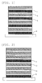
- Fig. 1 is a schematic view showing the cross section of a magnetic thin film of the first embodiment of the invention, in which the ratio of first magnetic layer/second magnetic layer is 1/1.
- a first magnetic layer 1 and a second magnetic layer 2 are alternatively laminated via an insulating layer 3 given therebetween.
- the first magnetic layer is so planned as to have a higher anisotropic magnetic field than the second magnetic layer 2, while on the other hand, the second magnetic layer 2 is so planned as to have a higher saturation magnetization than the first magnetic layer 1.
- the magnetic material to be used for the first magnetic layer 1 is preferably a magnetic material having a high anisotropic magnetic field, including, for example, a Co-Sm alloy, a 3d transition metal/rare earth metal alloy such as Co-Y, Co-Ce, Co-Pr, Co-La, Co-Nd, and a regular alloy of Fe-Pt or Co-Pt.
- the magnetic material to be used for the second magnetic layer 2 is preferably Co, Fe, and a 3d transition metal alloy including, for example, an Fe-Co alloy, an Fe-Ni alloy and a Co-Ni alloy.
- the insulating material to be used in the insulating layer 3 includes, for example, SiO 2 , Al 2 O 3 .
- first magnetic layer/second magnetic layer/insulating layer Co-Sm/Co/SiO 2 .
- first magnetic layer 1 having a thickness of 10 nm, using an induction-coupling RF sputtering apparatus under the following condition: (1) The atmosphere gas is Ar; (2) the pressure for film formation is 220 mPa; (3) the back pressure is at most 1.0x10 -5 Pa; and (4) the target is Co-Sm (Sm: 17 atm%).
- an insulating layer 3 having a thickness of 1 nm is formed on the above first magnetic layer 1.
- a second magnetic layer 2 having a thickness of 10 nm is formed on the insulating layer 3.
- an insulating layer 2 having a thickness of 1 nm is formed on the above second magnetic layer 2. This is repeated to fabricate a magnetic thin film laminate.
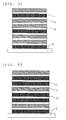
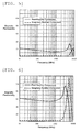
- Fig. 2 to Fig. 4 are modifications of this embodiment.
- three second magnetic layers are laminated on every one first magnetic layer; in the modification of Fig. 3, two second magnetic layers are laminated on every one first magnetic layer; and in the modification of Fig. 4, one second magnetic layer is laminated on every two first magnetic layers.
- These modifications may be produced by suitably forming the necessary constitutive layers each under the same condition as above.
- Fig. 5 to Fig. 8 are graphs showing the magnetic permeability-frequency characteristic of the magnetic thin films of Fig. 1 to Fig. 4, respectively.
- Fig. 5 is a graph of the magnetic thin film of Fig. 1;
- Fig. 6 is a graph of the magnetic thin film of Fig. 2;
- Fig. 7 is a graph of the magnetic thin film of Fig. 3;
- Fig. 8 is a graph of the magnetic thin film of Fig. 4.
- the thickness of the insulating layer 3 is described with reference to the graph of Fig. 9 that shows the relationship between the thickness of an insulating layer and the saturation magnetization and the anisotropic magnetic field of the magnetic thin film having the insulating layer. It is considered that the reduction in the anisotropic magnetic filed in accordance with the increase in the thickness of the insulating layer may be because of the sudden reduction in the exchange interaction between the first magnetic layer 1 and the second magnetic layer 2 in accordance with the increase in the thickness of the insulating layer. In particular, in the region where the thickness of the insulating layer is 1.6 nm or more, the anisotropic magnetic field is almost at a constant value of about 20 Oe or so.
- the value of the anisotropic magnetic field is nearly the same as the anisotropic magnetic field of a magnetic thin film formed of the second magnetic layer alone, and it may be presumed that this would be in a condition where the exchange interaction with the first magnetic layer 1 has almost disappeared. Accordingly, in these samples, it may be considered that the first magnetic layer 1 and the second magnetic layer 2 would almost independently work, and it may be presumed that the magnetization of the first magnetic layer having a high anisotropic magnetic layer would be almost inactive and that the magnetization movement of the second magnetic layer 2 alone may be observed.
- the high saturation magnetization layer and the high anisotropic magnetic field layer in the film must be coupled in a mode of exchange coupling therein, and therefore it is desirable that the thickness of the insulating layer 3 is at most 1 nm. Even when the thickness of the insulating layer 3 is 0, the magnetic film may show an anisotropic magnetic field over 2000 Oe just after its fabrication, but after aging with time or through thermal treatment, the characteristics of the magnetic material in the constitutive layers may worsen. Accordingly, the thickness of the insulating layer 3 is preferably at least 0.2 nm.
- Fig. 10 is a graph showing the relationship between the thickness of the first magnetic layer 1 that is changed to 10 nm, 20 nm, 30 nm, 40 nm, 70 nm and 140 nm, and the imaginary number part of the magnetic permeability of the magnetic thin film having the first magnetic layer.
- the samples are as follows: The first magnetic layers 1 each having the predetermined thickness are alternately laminated with the second magnetic layers 2 each having a thickness of 10 nm, the number of which is determined in accordance with the number of the first magnetic layers 1 so that the ratio of the first magnetic layers 1 to the second magnetic layers 2 could be 1/1, with inserting an insulating layer 3 having a thickness of 0.6 nm between the every two magnetic layers 1 and 2.
- the graph shows that the imaginary number component of the magnetic permeability forms a peak on the higher frequency side in the samples where the first magnetic layer 1 is thinner, but that the peak of the imaginary number component the magnetic permeability of the samples where the first magnetic layer 1 is thick is shifted to the low frequency side.
- the samples where the thickness of the first magnetic layer 1 is 40 nm or more have plural peaks of the imaginary number component of the magnetic permeability thereof. The reason why the samples have such plural peaks may be because of the existence of plural resonance modes inside the magnetic layers therein.
- the existence of such plural modes may be because of the following reasons: When the first magnetic layer 1 is thick, then there may exist a part adjacent to the second magnetic layer 2 and a part not adjacent to the second magnetic layer 2, thereby forming phases having a partially different anisotropic magnetic field, or the thick first magnetic layer 1 may have an anisotropic magnetic field distribution inside it of such that the anisotropic magnetic field of the interface region of the first magnetic layer 1 near to the second magnetic layer 2 differs from that of the inside region of the first magnetic layer 1 remote from the second magnetic layer 2.
- the thickness of the high anisotropic magnetic field layer and the high saturation magnetization layer is defined to be at most 30 nm each which does not cause the appearance of the plural peaks.
- the thickness of the magnetic layer is lower than 3 nm, then the magnetic film may be in an ultraparamagnetic state in which the magnetization of the film may be disturbed by thermal fluctuation and the film could no more show ferromagnetism. Accordingly, the thickness of the magnetic layer is preferably at least 3 nm.
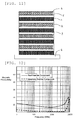
- the second embodiment of the high-frequency magnetic thin film of the invention is described with reference to Fig. 11 and Fig. 12.
- the magnetic thin film of Fig. 11 is a magnetic thin film laminate, in which the first magnetic layer 1 is a magnetic thin film formed of a Co-Sm alloy and the second magnetic layer 2 is a magnetic thin film having a granular structure that comprises magnetic particles 4 of an FeCo alloy enveloped with an insulator 5 of Si0 2 .
- Fig. 12 shows a magnetic permeability-frequency characteristic graph of a sample of the magnetic thin film of the second embodiment, in which the first magnetic layer 1 is a Co-Sm layer having a thickness of 10 nm, the second magnetic layer 2 is an FeCo (Fe: 60 atm%)-SiO 2 granular layer having a thickness of 20 nm, and the insulating layer 3 is an SiO 2 layer having a thickness of 0.5 nm.
- the sample has a magnetic permeability of around 20 and a resonance frequency of about 9 GHz, therefore having excellent high-frequency magnetic characteristics.
- the high saturation magnetization layer is a granular structure layer of an FeCo alloy; and the sample has such excellent magnetic characteristics like the other samples where the high saturation magnetization layer is a Co layer. It is understood that in this sample, the granular structure layer effectively functions as the high saturation magnetization layer therein.
- Fig. 13 shows an electronic device in which a magnetic thin film 7 is formed on a substrate 6 and a conductor 8 to constitute a plane coil is formed on the magnetic thin film 7.
- the magnetic thin film of the invention is used for the magnetic thin film 7, and the electronic device having the constitution is workable in a GHz-level band.
- This embodiment is an electronic device where a magnetic thin film is formed on a wiring board, but apart from it, the invention may also provide an electronic part to be fabricated by forming a magnetic thin film on an insulating substrate and processing it into individual chips.
- the invention can be used in electronic parts comprising a thin film magnetic material such as thin-film inductors, thin-film transformers, etc.
- the invention is utilized in circuit parts of electronic appliances to be used in a GHz-level band.
Landscapes
- Engineering & Computer Science (AREA)
- Chemical & Material Sciences (AREA)
- Crystallography & Structural Chemistry (AREA)
- Power Engineering (AREA)
- Nanotechnology (AREA)
- Composite Materials (AREA)
- Physics & Mathematics (AREA)
- Electromagnetism (AREA)
- Microelectronics & Electronic Packaging (AREA)
- Thin Magnetic Films (AREA)
- Coils Or Transformers For Communication (AREA)
Abstract
Description
- The present invention relates to a magnetic thin film capable of working in a GHz-order frequency band, and to an electronic device comprising it.
- With rapid popularization of mobile communication with typically mobile phones, a demand for communication appliances having a high transmission speed is increasing. A novel standard made for increasing the transmission speed of such mobile communication appliances is toward the increase in the working frequency thereof for avoiding a competition with the already-existing electric wave communications technology, and recently, the working frequency of mobile communication appliances has reached a GHz-order level. Accordingly, workability in a GHz band is one indispensable matter for the material to be used for the devices that meet the recent communication standard.
- The workability in such a high frequency band is required also for other electronic devices comprising a magnetic material, such as inductor, transformer, etc. However, since a magnetic material increases its loss through ferromagnetic resonance, the devices comprising it are difficult to work in a high-frequency band. For realizing the reduction in the loss of magnetic material in a high-frequency band, it is desirable to increase the saturation magnetization of the material and the anisotropic magnetic field around it to thereby increase the resonance frequency of the material. For obtaining a magnetic material having the characteristics, proposed is a magnetic thin film of a thin magnetic layer and a thin insulating layer alternately laminated on each other.
- Patent Reference 1:
JP-A-9-063844 - Patent Reference 2:
JP-A-2003-338409 - It is known that the resonance frequency of a magnetic thin film depends on the product of the saturation magnetization and the anisotropic magnetic field thereof, as in the following formula (1) wherein fr indicates the resonance frequency, Ms indicates the saturation magnetization, and Hk indicates the anisotropic magnetic field.
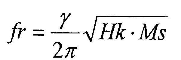
(In this, y indicates a gyro magnetic constant.) - A magnetic material has an almost constant saturation magnetization value, and therefore, it has heretofore been considered that the method of increasing the resonance frequency of the material could be attained by actually increasing the anisotropic magnetic filed to thereby increase the magnetization rotation of the material. For the method of increasing the anisotropic magnetic field of a magnetic material, known are (1) thermal treatment of the material in a magnetic film to thereby impart induced magnetic anisotropy thereto, (2) forming a slit through a magnetic thin film to thereby impart profile magnetic anisotropy thereto, and (3) exchange coupling between a ferromagnetic film and an antiferromagnetic film. However, the above are problematic in that the process (1) is complicated as requiring thermal treatment, the process (2) results in substantial reduction in the magnetic permeability of the slit-formed magnetic thin film since the magnetic permeability of the slit part of the film is lost, and the process (3) results in the reduction in the magnetic permeability of the laminate structure since the antiferromagnetic film is formed and the saturation magnetization of the overall magnetic film laminate is thereby lowered.
- Fig. 14 is a graph showing the change of the saturation magnetization and the anisotropic magnetic field of an FeCo alloy magnetic material, depending on the Fe proportion in the alloy. From this, it is known that the increase in the saturation magnetization tends to the reduction in the anisotropic magnetic field. As in this, the alloy could hardly satisfy both a high saturation magnetization and a high anisotropic magnetic field, and therefore it is difficult for one and the same kind of a magnetic material to satisfy both a high saturation magnetization and a high anisotropic magnetic field, therefore attaining a reduced loss and an increased resonance frequency in a high-frequency band. In particular, it is extremely difficult to realize the characteristics necessary for obtaining electronic devices that may work in a GHz-level band.
- The present invention is to solve the above-mentioned problems and to provide a magnetic thin film having a high saturation magnetization and a high anisotropic magnetic field and to provide an electronic device capable of effectively working in a GHz-level band.
- The invention proposes a high-frequency magnetic thin film comprising a magnetic layer and an insulating layer that are laminated alternately, wherein the magnetic layer includes a first magnetic layer and a second magnetic layer, the first magnetic layer has a higher anisotropic magnetic field than the second magnetic layer, and the second magnetic layer has a higher saturation magnetization than the first magnetic layer.
- According to the invention, a first magnetic layer and a second magnetic layer are laminated whereby the anisotropic magnetic field of the first magnetic layer may be increased up to the extremity and the saturation magnetization of the second magnetic layer may be increased up to the extremity with the result that the saturation magnetization of the second magnetic layer may compensate for that of the first magnetic layer and the anisotropic magnetic field of the first magnetic layer may compensate for that of the second magnetic layer. The respective magnetic layers are separated from each other by the insulating layer put therebetween, and are thus alternately laminated, and accordingly, the magnetic materials of the two layers do not mix and the two layers may fully express their own excellent characteristics. As a result, the resonance frequency of the magnetic thin film may be increased.
- The invention also proposes a high-frequency magnetic thin film wherein the first magnetic layer comprises essentially an alloy of a rare earth metal and a ferromagnetic 3d transition metal; and a high-frequency magnetic thin film wherein the second magnetic layer comprises essentially a ferromagnetic 3d transition metal or its alloy. The invention also proposes a high-frequency magnetic thin film wherein the rare earth metal is Sm; and a high-frequency magnetic thin film wherein the 3d transition metal is Co.
- According to the invention, the first magnetic layer may comprise essentially an alloy of a 3d transition metal (at least one of Fe, Co and Ni) and a rare earth metal (at least one of Sm, Pr, Ce, Y, Nd and La), and therefore the magnetic layer may have a higher anisotropic magnetic field (at least 1000 Oe) than an ordinary anisotropic magnetic field (from 100 to 150 Oe). The second magnetic layer may comprise essentially a ferromagnetic 3d transition metal or its alloy, and therefore the saturation magnetization of the magnetic layer may be high. When the rare earth metal is Sm and the 3d transition metal is Co therein, then the anisotropic magnetic field of the magnetic layer may be the highest.
- The invention also proposes a high-frequency magnetic thin film wherein the first magnetic layer or the second magnetic layer has a granular structure of a magnetic particle enveloped with an insulating material.
- According to the invention, the magnetic layer may have a granular structure as above, whereby the insulation resistance of the magnetic thin film may be increased and the eddy-current loss in the high-frequency magnetic permeability characteristics of the film may be greatly reduced.
- The invention also proposes a high-frequency magnetic thin film wherein the first magnetic layer and the second magnetic layer are coupled in a mode of exchange coupling with each other via the insulating layer given therebetween. The invention also proposes a high-frequency magnetic thin film wherein the first magnetic layer and the second magnetic layer are regularly laminated via the insulating layer given therebetween.
- According to the invention, the first magnetic layer and the second magnetic layer are coupled in a mode of exchange coupling with each other at their interfaces via the insulating layer given therebetween, whereby the anisotropic magnetic field of the respective layers is averaged. In the invention, the first magnetic layer and the second magnetic layer are regularly laminated at a predetermined ratio and therefore, the proportion of the respective layers and the thickness thereof may be controlled. Accordingly, the saturation magnetization and the anisotropic magnetic field of the film of the invention may be change in a broad range, and the magnetic permeability and the resonance frequency thereof may be controlled within a predetermined range. "Exchange coupling" as referred to herein is defined as a condition of exchange interaction between different magnetic layers.
- The invention also proposes a high-frequency electronic device comprising a magnetic thin film and a conductor of a conductive metal, wherein the magnetic thin film comprises an insulating layer and a magnetic layer that are laminated alternately, the magnetic layer includes a first magnetic layer and a second magnetic layer, the first magnetic layer has a higher anisotropic magnetic field than the second magnetic layer, the second magnetic layer has a higher saturation magnetization than the first magnetic layer, and the conductor having a predetermined shape is formed on the magnetic thin film.
- According to the invention, an electronic device with little loss can be obtained that can work in a GHz-level band.
- As in the above, the invention has realized a magnetic thin film having a high saturation magnetization and a high anisotropic magnetic field as compared with conventional magnetic thin films, and having a reduced loss and an increased resonance frequency in a high-frequency zone, and the invention has also realized an electronic device capable of working in a GHz-level band.
-
- Fig. 1 is a schematic view showing the cross section of a magnetic thin film of a first embodiment of the invention.
- Fig. 2 is a schematic view showing the cross section of another magnetic thin film of the first embodiment of the invention.
- Fig. 3 is a schematic view showing the cross section of still another magnetic thin film of the first embodiment of the invention.
- Fig. 4 is a schematic view showing the cross section of still another magnetic thin film of the first embodiment of the invention.
- Fig. 5 is a magnetic permeability-frequency characteristic graph of the magnetic thin film of Fig. 1.
- Fig. 6 is a magnetic permeability-frequency characteristic graph of the magnetic thin film of Fig. 2.
- Fig. 7 is a magnetic permeability-frequency characteristic graph of the magnetic thin film of Fig. 3.
- Fig. 8 is a magnetic permeability-frequency characteristic graph of the magnetic thin film of Fig. 4.
- Fig. 9 is a graph showing the relationship between the thickness of an insulating layer and the saturation magnetization and the anisotropic magnetic field of the magnetic thin film having the insulating layer.
- Fig. 10 is a graph showing the relationship between the thickness of the first magnetic layer and the imaginary number part of the magnetic permeability of the magnetic thin film having the first magnetic layer.
- Fig. 11 is a schematic view showing the cross section of a magnetic thin film of a second embodiment of the invention.
- Fig. 12 is a magnetic permeability-frequency characteristic graph of the magnetic thin film of the second embodiment of the invention.
- Fig. 13 is a perspective view showing an electronic device of the invention.
- Fig. 14 is a graph showing the relationship between the saturation magnetization and the anisotropic magnetic field of an FeCo alloy magnetic material.
- In these drawings, 1 is a first magnetic layer, 2 is a second magnetic layer, 3 is an insulating layer, 4 is a magnetic particle, 5 is an insulator, 6 is a substrate, 7 is a magnetic thin film, 8 is a conductor.
- The first embodiment of the high-frequency magnetic thin film of the invention is described with reference to its drawings. Fig. 1 is a schematic view showing the cross section of a magnetic thin film of the first embodiment of the invention, in which the ratio of first magnetic layer/second magnetic layer is 1/1. In the magnetic thin film, a first
magnetic layer 1 and a secondmagnetic layer 2 are alternatively laminated via aninsulating layer 3 given therebetween. The first magnetic layer is so planned as to have a higher anisotropic magnetic field than the secondmagnetic layer 2, while on the other hand, the secondmagnetic layer 2 is so planned as to have a higher saturation magnetization than the firstmagnetic layer 1. The magnetic material to be used for the firstmagnetic layer 1 is preferably a magnetic material having a high anisotropic magnetic field, including, for example, a Co-Sm alloy, a 3d transition metal/rare earth metal alloy such as Co-Y, Co-Ce, Co-Pr, Co-La, Co-Nd, and a regular alloy of Fe-Pt or Co-Pt. The magnetic material to be used for the secondmagnetic layer 2 is preferably Co, Fe, and a 3d transition metal alloy including, for example, an Fe-Co alloy, an Fe-Ni alloy and a Co-Ni alloy. The insulating material to be used in the insulatinglayer 3 includes, for example, SiO2, Al2O3. - One example of a production method for the magnetic film is described, having a constitution of first magnetic layer/second magnetic layer/insulating layer = Co-Sm/Co/SiO2. For example, on an insulating substrate S such as Si or Al2O3, formed is a first
magnetic layer 1 having a thickness of 10 nm, using an induction-coupling RF sputtering apparatus under the following condition: (1) The atmosphere gas is Ar; (2) the pressure for film formation is 220 mPa; (3) the back pressure is at most 1.0x10⁻⁵ Pa; and (4) the target is Co-Sm (Sm: 17 atm%). Next, under the same condition but changing the target to SiO2, an insulatinglayer 3 having a thickness of 1 nm is formed on the above firstmagnetic layer 1. Next, also under the same condition but changing the target to Co, a secondmagnetic layer 2 having a thickness of 10 nm is formed on the insulatinglayer 3. Further, an insulatinglayer 2 having a thickness of 1 nm is formed on the above secondmagnetic layer 2. This is repeated to fabricate a magnetic thin film laminate. - Fig. 2 to Fig. 4 are modifications of this embodiment. In the modification of Fig. 2, three second magnetic layers are laminated on every one first magnetic layer; in the modification of Fig. 3, two second magnetic layers are laminated on every one first magnetic layer; and in the modification of Fig. 4, one second magnetic layer is laminated on every two first magnetic layers. These modifications may be produced by suitably forming the necessary constitutive layers each under the same condition as above.
- Fig. 5 to Fig. 8 are graphs showing the magnetic permeability-frequency characteristic of the magnetic thin films of Fig. 1 to Fig. 4, respectively. Fig. 5 is a graph of the magnetic thin film of Fig. 1; Fig. 6 is a graph of the magnetic thin film of Fig. 2; Fig. 7 is a graph of the magnetic thin film of Fig. 3; Fig. 8 is a graph of the magnetic thin film of Fig. 4. These show that all the magnetic thin films have a resonance frequency of at least 3 GHz. This means that the saturation magnetization and the anisotropic magnetic field of the films are increased with the result that the product of Hk and Ms in the formula (1) is on the level of a GHz band. Comparing these graphs shows that, when the proportion of the second
magnetic layer 2 is larger, then the magnetic permeability is higher; but on the contrary, when the proportion of the firstmagnetic layer 1 is larger, then the resonance frequency is higher. This means that, when the proportion of the secondmagnetic layer 2 is larger, then the saturation magnetization is increased and the magnetic permeability is thereby increased, and that, when the proportion of the firstmagnetic layer 1 is larger, then the anisotropic magnetic field is increased and the resonance frequency is thereby increased, therefore resulting in that the secondmagnetic layer 2 and the firstmagnetic layer 1 effectively function as a high saturation magnetization layer and a high anisotropic magnetic field layer, respectively. - The thickness of the insulating
layer 3 is described with reference to the graph of Fig. 9 that shows the relationship between the thickness of an insulating layer and the saturation magnetization and the anisotropic magnetic field of the magnetic thin film having the insulating layer. It is considered that the reduction in the anisotropic magnetic filed in accordance with the increase in the thickness of the insulating layer may be because of the sudden reduction in the exchange interaction between the firstmagnetic layer 1 and the secondmagnetic layer 2 in accordance with the increase in the thickness of the insulating layer. In particular, in the region where the thickness of the insulating layer is 1.6 nm or more, the anisotropic magnetic field is almost at a constant value of about 20 Oe or so. The value of the anisotropic magnetic field is nearly the same as the anisotropic magnetic field of a magnetic thin film formed of the second magnetic layer alone, and it may be presumed that this would be in a condition where the exchange interaction with the firstmagnetic layer 1 has almost disappeared. Accordingly, in these samples, it may be considered that the firstmagnetic layer 1 and the secondmagnetic layer 2 would almost independently work, and it may be presumed that the magnetization of the first magnetic layer having a high anisotropic magnetic layer would be almost inactive and that the magnetization movement of the secondmagnetic layer 2 alone may be observed. For obtaining a high anisotropic magnetic field necessary for improving the high-frequency magnetic characteristics of a high-frequency magnetic film, the high saturation magnetization layer and the high anisotropic magnetic field layer in the film must be coupled in a mode of exchange coupling therein, and therefore it is desirable that the thickness of the insulatinglayer 3 is at most 1 nm. Even when the thickness of the insulatinglayer 3 is 0, the magnetic film may show an anisotropic magnetic field over 2000 Oe just after its fabrication, but after aging with time or through thermal treatment, the characteristics of the magnetic material in the constitutive layers may worsen. Accordingly, the thickness of the insulatinglayer 3 is preferably at least 0.2 nm. - The thickness of the magnetic layer is described with reference to Fig. 10. Fig. 10 is a graph showing the relationship between the thickness of the first
magnetic layer 1 that is changed to 10 nm, 20 nm, 30 nm, 40 nm, 70 nm and 140 nm, and the imaginary number part of the magnetic permeability of the magnetic thin film having the first magnetic layer. The samples are as follows: The firstmagnetic layers 1 each having the predetermined thickness are alternately laminated with the secondmagnetic layers 2 each having a thickness of 10 nm, the number of which is determined in accordance with the number of the firstmagnetic layers 1 so that the ratio of the firstmagnetic layers 1 to the secondmagnetic layers 2 could be 1/1, with inserting an insulatinglayer 3 having a thickness of 0.6 nm between the every twomagnetic layers - The graph shows that the imaginary number component of the magnetic permeability forms a peak on the higher frequency side in the samples where the first
magnetic layer 1 is thinner, but that the peak of the imaginary number component the magnetic permeability of the samples where the firstmagnetic layer 1 is thick is shifted to the low frequency side. In particular, it is seen that the samples where the thickness of the firstmagnetic layer 1 is 40 nm or more have plural peaks of the imaginary number component of the magnetic permeability thereof. The reason why the samples have such plural peaks may be because of the existence of plural resonance modes inside the magnetic layers therein. It may be considered that the existence of such plural modes may be because of the following reasons: When the firstmagnetic layer 1 is thick, then there may exist a part adjacent to the secondmagnetic layer 2 and a part not adjacent to the secondmagnetic layer 2, thereby forming phases having a partially different anisotropic magnetic field, or the thick firstmagnetic layer 1 may have an anisotropic magnetic field distribution inside it of such that the anisotropic magnetic field of the interface region of the firstmagnetic layer 1 near to the secondmagnetic layer 2 differs from that of the inside region of the firstmagnetic layer 1 remote from the secondmagnetic layer 2. For effectively increasing the anisotropic magnetic field of the thin magnetic film and for thereby making the film have improved high-frequency magnetic characteristics, it is desirable that the thickness of the high anisotropic magnetic field layer and the high saturation magnetization layer is defined to be at most 30 nm each which does not cause the appearance of the plural peaks. When the thickness of the magnetic layer is lower than 3 nm, then the magnetic film may be in an ultraparamagnetic state in which the magnetization of the film may be disturbed by thermal fluctuation and the film could no more show ferromagnetism. Accordingly, the thickness of the magnetic layer is preferably at least 3 nm. - The second embodiment of the high-frequency magnetic thin film of the invention is described with reference to Fig. 11 and Fig. 12. The magnetic thin film of Fig. 11 is a magnetic thin film laminate, in which the first
magnetic layer 1 is a magnetic thin film formed of a Co-Sm alloy and the secondmagnetic layer 2 is a magnetic thin film having a granular structure that comprisesmagnetic particles 4 of an FeCo alloy enveloped with an insulator 5 of Si02. - Fig. 12 shows a magnetic permeability-frequency characteristic graph of a sample of the magnetic thin film of the second embodiment, in which the first
magnetic layer 1 is a Co-Sm layer having a thickness of 10 nm, the secondmagnetic layer 2 is an FeCo (Fe: 60 atm%)-SiO2 granular layer having a thickness of 20 nm, and the insulatinglayer 3 is an SiO2 layer having a thickness of 0.5 nm. The sample has a magnetic permeability of around 20 and a resonance frequency of about 9 GHz, therefore having excellent high-frequency magnetic characteristics. In this sample, the high saturation magnetization layer is a granular structure layer of an FeCo alloy; and the sample has such excellent magnetic characteristics like the other samples where the high saturation magnetization layer is a Co layer. It is understood that in this sample, the granular structure layer effectively functions as the high saturation magnetization layer therein. - An embodiment of the electronic device of the invention is described with reference to Fig. 13. Fig. 13 shows an electronic device in which a magnetic
thin film 7 is formed on asubstrate 6 and aconductor 8 to constitute a plane coil is formed on the magneticthin film 7. In this device, the magnetic thin film of the invention is used for the magneticthin film 7, and the electronic device having the constitution is workable in a GHz-level band. This embodiment is an electronic device where a magnetic thin film is formed on a wiring board, but apart from it, the invention may also provide an electronic part to be fabricated by forming a magnetic thin film on an insulating substrate and processing it into individual chips. - While the invention has been described in detail and with reference to specific embodiments thereof, it will be apparent to one skilled in the art that the invention should not be limited to the above-mentioned embodiments but various changes and modifications can be made therein without departing from the spirit and scope of the invention.
- The invention can be used in electronic parts comprising a thin film magnetic material such as thin-film inductors, thin-film transformers, etc. In particular, the invention is utilized in circuit parts of electronic appliances to be used in a GHz-level band.
Claims (12)
- A high-frequency magnetic thin film comprising a magnetic layer and an insulating layer that are laminated alternately, wherein the magnetic layer includes a first magnetic layer and a second magnetic layer, the first magnetic layer has a higher anisotropic magnetic field than the second magnetic layer, and the second magnetic layer has a higher saturation magnetization than the first magnetic layer.
- The high-frequency magnetic thin film as claimed in claim 1, wherein the first magnetic layer comprises essentially an alloy of a rare earth metal and a ferromagnetic 3d transition metal.
- The high-frequency magnetic thin film as claimed in claim 1, wherein the second magnetic layer comprises essentially a ferromagnetic 3d transition metal or its alloy.
- The high-frequency magnetic thin film as claimed in claim 1, wherein the first magnetic layer has a granular structure of a magnetic particle enveloped with an insulating material.
- The high-frequency magnetic thin film as claimed in claim 1, wherein the second magnetic layer has a granular structure of a magnetic particle enveloped with an insulating material.
- The high-frequency magnetic thin film as claimed in claim 2, wherein the rare earth metal is Sm.
- The high-frequency magnetic thin film as claimed in claim 2 or 3, wherein the 3d transition metal is Co.
- The high-frequency magnetic thin film as claimed in claim 1, wherein the first magnetic layer and the second magnetic layer are coupled in a mode of exchange coupling with each other via the insulating layer given therebetween.
- The high-frequency magnetic thin film as claimed in claim 1, wherein the first magnetic layer and the second magnetic layer are regularly laminated via the insulating layer given therebetween.
- The high-frequency magnetic thin film as claimed in claim 1, wherein the thickness of the insulating layer is from 0.2 to 1 nm.
- The high-frequency magnetic thin film as claimed in claim 1, wherein the thickness of the magnetic layer is from 3 to 30 nm.
- A high-frequency electronic device comprising a magnetic thin film and a conductor of a conductive metal formed on the magnetic thin film, wherein the magnetic thin film comprises an insulating layer and a magnetic layer that are laminated alternately, the magnetic layer includes a first magnetic layer and a second magnetic layer, the first magnetic layer has a higher anisotropic magnetic field than the second magnetic layer, the second magnetic layer has a higher saturation magnetization than the first magnetic layer, and the conductor having a predetermined shape is formed on the magnetic thin film.
Applications Claiming Priority (1)
| Application Number | Priority Date | Filing Date | Title |
|---|---|---|---|
| JP2006110238A JP4773254B2 (en) | 2006-03-15 | 2006-03-15 | High frequency magnetic thin film and high frequency electronic device |
Publications (1)
| Publication Number | Publication Date |
|---|---|
| EP1835515A1 true EP1835515A1 (en) | 2007-09-19 |
Family
ID=38226458
Family Applications (1)
| Application Number | Title | Priority Date | Filing Date |
|---|---|---|---|
| EP07251075A Withdrawn EP1835515A1 (en) | 2006-03-15 | 2007-03-14 | High-frequency magnetic thin film and high-frequency electronic device |
Country Status (3)
| Country | Link |
|---|---|
| US (1) | US7803470B2 (en) |
| EP (1) | EP1835515A1 (en) |
| JP (1) | JP4773254B2 (en) |
Families Citing this family (13)
| Publication number | Priority date | Publication date | Assignee | Title |
|---|---|---|---|---|
| JP2006086421A (en) * | 2004-09-17 | 2006-03-30 | Taiyo Yuden Co Ltd | Laminate magnetic thin film and its manufacturing method |
| JP2009080413A (en) | 2007-09-27 | 2009-04-16 | Fujinon Corp | Imaging optical system, image pickup apparatus for endoscope |
| JP2014195059A (en) * | 2013-02-27 | 2014-10-09 | Shinko Electric Ind Co Ltd | Electronic apparatus |
| CN108698369B (en) * | 2016-03-04 | 2021-03-09 | 3M创新有限公司 | Magnetic multilayer sheet |
| EP3490358B1 (en) * | 2016-07-22 | 2023-08-09 | Maxell, Ltd. | Electromagnetic absorber |
| CN108022751B (en) | 2016-10-31 | 2022-01-11 | 北京北方华创微电子装备有限公司 | Deposition method of magnetic thin film lamination, magnetic thin film lamination and micro-inductance device |
| US11626228B2 (en) * | 2016-12-22 | 2023-04-11 | Rogers Corporation | Multi-layer magneto-dielectric material |
| CN107146690B (en) | 2017-03-03 | 2019-11-05 | 华为机器有限公司 | Thin film inductor, power conversion circuit and chip |
| JP7181064B2 (en) * | 2018-11-21 | 2022-11-30 | 公益財団法人電磁材料研究所 | FERROMAGNETIC LAMINATED FILM AND MANUFACTURING METHOD THEREOF AND ELECTROMAGNETIC INDUCTIVE ELECTRONIC COMPONENTS |
| CN114286265A (en) * | 2020-09-28 | 2022-04-05 | 青岛海信激光显示股份有限公司 | Sound production screen and projection television |
| US12322695B2 (en) * | 2020-12-01 | 2025-06-03 | Ferric Inc. | Magnetic core with hard ferromagnetic biasing layers and structures containing same |
| US12224091B2 (en) | 2021-07-16 | 2025-02-11 | Ferric Inc. | Ferromagnetic-polymer composite material and structures comprising same |
| US12125713B2 (en) | 2022-03-22 | 2024-10-22 | Ferric Inc. | Method for manufacturing ferromagnetic-dielectric composite material |
Citations (3)
| Publication number | Priority date | Publication date | Assignee | Title |
|---|---|---|---|---|
| US5789069A (en) * | 1992-08-27 | 1998-08-04 | Tdk Corporation | Magnetic multilayer film and magnetoresistance element |
| EP1450378A2 (en) * | 2003-02-24 | 2004-08-25 | TDK Corporation | Soft magnetic member, method for manufacturing thereof and electromagnetic wave controlling sheet |
| US20040209098A1 (en) * | 2001-01-18 | 2004-10-21 | Taiyo Yuden Co., Ltd. | Granular magnetic thin film and method for making the same, multilayered magnetic film, magnetic components and electronic equipment |
Family Cites Families (31)
| Publication number | Priority date | Publication date | Assignee | Title |
|---|---|---|---|---|
| JPH0270085A (en) * | 1988-09-02 | 1990-03-08 | Sony Corp | Production of amorphous soft magnetic film |
| JPH08138228A (en) * | 1994-11-11 | 1996-05-31 | Hitachi Ltd | Magnetic recording medium, method of manufacturing magnetic recording medium, and magnetic recording device |
| JPH0963844A (en) | 1995-08-23 | 1997-03-07 | Toshiba Corp | Laminated magnetic film and thin film magnetic element using the same |
| US5695864A (en) * | 1995-09-28 | 1997-12-09 | International Business Machines Corporation | Electronic device using magnetic components |
| US6313973B1 (en) * | 1998-06-30 | 2001-11-06 | Kabushiki Kaisha Toshiba | Laminated magnetorestrictive element of an exchange coupling film, an antiferromagnetic film and a ferromagnetic film and a magnetic disk drive using same |
| US6455174B1 (en) * | 1998-11-05 | 2002-09-24 | Hitachi Maxell, Ltd. | Magnetic recording medium, recording and reproducing head, and magnetic recording and reproducing method |
| US6731446B2 (en) * | 2000-02-03 | 2004-05-04 | Matsushita Electric Industrial Co., Ltd. | Method for forming a magnetic pattern in a magnetic recording medium, method for producing a magnetic recording medium, magnetic pattern forming device, magnetic recording medium and magnetic recording device |
| EP1156479A3 (en) * | 2000-05-16 | 2007-01-24 | Matsushita Electric Industrial Co., Ltd. | Magnetic recording medium, its production method and magnetic recording apparatus |
| JP2002358616A (en) * | 2000-06-12 | 2002-12-13 | Toshiba Corp | Magnetic recording medium and magnetic recording device |
| JP3665261B2 (en) * | 2000-09-01 | 2005-06-29 | 株式会社日立製作所 | Perpendicular magnetic recording medium and magnetic storage device |
| US6816330B2 (en) * | 2000-12-22 | 2004-11-09 | Matsushita Electric Industrial Co., Ltd. | Method for forming a magnetic pattern in a magnetic recording medium, magnetic recording medium magnetic recording device and photomask |
| US6713195B2 (en) * | 2001-01-05 | 2004-03-30 | Nve Corporation | Magnetic devices using nanocomposite materials |
| JP2002222520A (en) * | 2001-01-24 | 2002-08-09 | Mitsubishi Chemicals Corp | Magnetic pattern forming method, magnetic pattern forming apparatus, magnetic disk and magnetic recording apparatus |
| US6650513B2 (en) * | 2001-01-29 | 2003-11-18 | International Business Machines Corporation | Magnetic devices with a ferromagnetic layer having perpendicular magnetic anisotropy and an antiferromagnetic layer for perpendicularly exchange biasing the ferromagnetic layer |
| JP2003016620A (en) * | 2001-06-29 | 2003-01-17 | Toshiba Corp | Magnetic recording medium, magnetic recording device, and magnetic recording method |
| US6835475B2 (en) * | 2001-07-26 | 2004-12-28 | Hitachi Global Storage Technologies Netherlands B.V. | Dual-layer perpendicular magnetic recording media with laminated underlayer formed with antiferromagnetically coupled films |
| JP2004005874A (en) * | 2001-08-07 | 2004-01-08 | Mitsubishi Chemicals Corp | Method and method for forming magnetic pattern of magnetic recording medium, magnetic pattern forming apparatus, magnetic recording medium, and magnetic recording apparatus |
| JP3793725B2 (en) * | 2002-01-25 | 2006-07-05 | アルプス電気株式会社 | Magnetic detection element, method of manufacturing the same, and magnetic detection apparatus using the magnetic detection element |
| JP3680035B2 (en) * | 2002-03-29 | 2005-08-10 | 株式会社東芝 | Magnetic recording apparatus and magnetic recording method |
| JP2003303456A (en) * | 2002-04-09 | 2003-10-24 | Canon Inc | Magneto-optical recording medium and manufacturing method thereof |
| JP2003317337A (en) * | 2002-04-26 | 2003-11-07 | Canon Inc | Magneto-optical recording medium and recording method |
| JP2003338409A (en) * | 2002-05-22 | 2003-11-28 | Taiyo Yuden Co Ltd | Laminated magnetic thin film |
| JP2004039033A (en) * | 2002-06-28 | 2004-02-05 | Toshiba Corp | Magnetic recording medium and magnetic recording / reproducing device |
| JP2004110917A (en) * | 2002-09-18 | 2004-04-08 | Hitachi Ltd | Magnetic recording medium, magnetic disk device using the same, and method of manufacturing the same |
| JP2004207651A (en) * | 2002-12-26 | 2004-07-22 | Tdk Corp | Magnetic thin film for high frequency, composite magnetic thin film and magnetic element using the same |
| JP2004235355A (en) * | 2003-01-29 | 2004-08-19 | Tdk Corp | Soft magnetic member and magnetic element using the same |
| JP2004259787A (en) * | 2003-02-24 | 2004-09-16 | Tdk Corp | Soft magnetic member, electromagnetic wave control sheet and method for manufacturing soft magnetic member |
| US20080206891A1 (en) | 2003-11-12 | 2008-08-28 | Wang Shan X | Synthetic antiferromagnetic nanoparticles |
| US7199984B2 (en) * | 2004-03-16 | 2007-04-03 | Hitachi Global Storage Technologies Netherlands B.V. | Current-perpendicular-to-plane magnetoresistive sensor with free layer stabilized by in-stack orthogonal magnetic coupling |
| US7230265B2 (en) * | 2005-05-16 | 2007-06-12 | International Business Machines Corporation | Spin-polarization devices using rare earth-transition metal alloys |
| US20070096229A1 (en) * | 2005-10-28 | 2007-05-03 | Masatoshi Yoshikawa | Magnetoresistive element and magnetic memory device |
-
2006
- 2006-03-15 JP JP2006110238A patent/JP4773254B2/en not_active Expired - Fee Related
-
2007
- 2007-03-14 EP EP07251075A patent/EP1835515A1/en not_active Withdrawn
- 2007-03-14 US US11/724,458 patent/US7803470B2/en not_active Expired - Fee Related
Patent Citations (3)
| Publication number | Priority date | Publication date | Assignee | Title |
|---|---|---|---|---|
| US5789069A (en) * | 1992-08-27 | 1998-08-04 | Tdk Corporation | Magnetic multilayer film and magnetoresistance element |
| US20040209098A1 (en) * | 2001-01-18 | 2004-10-21 | Taiyo Yuden Co., Ltd. | Granular magnetic thin film and method for making the same, multilayered magnetic film, magnetic components and electronic equipment |
| EP1450378A2 (en) * | 2003-02-24 | 2004-08-25 | TDK Corporation | Soft magnetic member, method for manufacturing thereof and electromagnetic wave controlling sheet |
Also Published As
| Publication number | Publication date |
|---|---|
| JP4773254B2 (en) | 2011-09-14 |
| US20070218273A1 (en) | 2007-09-20 |
| JP2007251111A (en) | 2007-09-27 |
| US7803470B2 (en) | 2010-09-28 |
Similar Documents
| Publication | Publication Date | Title |
|---|---|---|
| US7803470B2 (en) | High-frequency magnetic thin film and high-frequency electronic device | |
| Ohnuma et al. | Magnetostriction and soft magnetic properties of (Co 1− x Fe x)–Al–O granular films with high electrical resistivity | |
| Ikeda et al. | Multilayer nanogranular magnetic thin films for GHz applications | |
| US6542060B2 (en) | Microcomponent of the microinductor or microtransformer type | |
| EP1473742A1 (en) | High-frequency magnetic thin film, composite magnetic thin film, and magnetic device using same | |
| Luborsky et al. | Potential of amorphous alloys for application in magnetic devices | |
| EP0637038B1 (en) | Magnetic core for pulse transformer and pulse transformer made thereof | |
| JP2001160510A (en) | Coil device | |
| Tumanski | Modern magnetic materials-the review | |
| US5609946A (en) | High frequency, high density, low profile, magnetic circuit components | |
| US20060068228A1 (en) | Laminated magnetic thin film and method of manufacturing the same | |
| EP1450378A2 (en) | Soft magnetic member, method for manufacturing thereof and electromagnetic wave controlling sheet | |
| JP2002158486A (en) | Electromagnetic wave absorbing film | |
| EP0849747B1 (en) | Noise-limiting transformer apparatus | |
| Alves et al. | Soft magnetic materials for electrical engineering: State of the art and recent advances | |
| CN104465017A (en) | Nd-doped CoZr-base high-frequency soft magnetic film and preparation method thereof | |
| KR100742555B1 (en) | Magnetic thin film for high frequency and its production method, and magnetic element | |
| HK1103161A (en) | High-frequency magnetic thin film and high-frequency electronic device | |
| JP4097160B2 (en) | Method for manufacturing electromagnetic interference suppressor | |
| Munakata et al. | Very high electrical resistivity and heteroamorphous structure of soft magnetic (Co/sub 35.6/Fe/sub 50/B/sub 14.4/)-(SiO/sub 2/) thin films | |
| US6529110B2 (en) | Microcomponent of the microinductor or microtransformer type | |
| JPWO2005027154A1 (en) | Magnetic thin film for high frequency, its manufacturing method and magnetic element | |
| JP2000252121A (en) | HIGH-FREQUENCY Co-BASED METALLIC AMORPHOUS MAGNETIC FILM, AND MAGNETIC ELEMENT, INDUCTOR AND TRANSFORMER USING THE SAME | |
| EP1734542A1 (en) | Electromagnetic noise suppressing thin film | |
| Ha et al. | High frequency characteristics and magnetic properties of CoFeN/native-oxide multilayer films |
Legal Events
| Date | Code | Title | Description |
|---|---|---|---|
| PUAI | Public reference made under article 153(3) epc to a published international application that has entered the european phase |
Free format text: ORIGINAL CODE: 0009012 |
|
| AK | Designated contracting states |
Kind code of ref document: A1 Designated state(s): AT BE BG CH CY CZ DE DK EE ES FI FR GB GR HU IE IS IT LI LT LU LV MC MT NL PL PT RO SE SI SK TR |
|
| AX | Request for extension of the european patent |
Extension state: AL BA HR MK YU |
|
| 17P | Request for examination filed |
Effective date: 20070926 |
|
| REG | Reference to a national code |
Ref country code: HK Ref legal event code: DE Ref document number: 1103161 Country of ref document: HK |
|
| 17Q | First examination report despatched |
Effective date: 20071227 |
|
| AKX | Designation fees paid |
Designated state(s): AT BE BG CH CY CZ DE DK EE ES FI FR GB GR HU IE IS IT LI LT LU LV MC MT NL PL PT RO SE SI SK TR |
|
| STAA | Information on the status of an ep patent application or granted ep patent |
Free format text: STATUS: THE APPLICATION IS DEEMED TO BE WITHDRAWN |
|
| 18D | Application deemed to be withdrawn |
Effective date: 20101001 |
|
| REG | Reference to a national code |
Ref country code: HK Ref legal event code: WD Ref document number: 1103161 Country of ref document: HK |