EP1835513A1 - Electronic device and method for manufacturing same - Google Patents
Electronic device and method for manufacturing same Download PDFInfo
- Publication number
- EP1835513A1 EP1835513A1 EP05822381A EP05822381A EP1835513A1 EP 1835513 A1 EP1835513 A1 EP 1835513A1 EP 05822381 A EP05822381 A EP 05822381A EP 05822381 A EP05822381 A EP 05822381A EP 1835513 A1 EP1835513 A1 EP 1835513A1
- Authority
- EP
- European Patent Office
- Prior art keywords
- region
- transparent conductive
- conductive film
- ultraviolet light
- electronic device
- Prior art date
- Legal status (The legal status is an assumption and is not a legal conclusion. Google has not performed a legal analysis and makes no representation as to the accuracy of the status listed.)
- Withdrawn
Links
Images



Classifications
-
- H—ELECTRICITY
- H01—ELECTRIC ELEMENTS
- H01B—CABLES; CONDUCTORS; INSULATORS; SELECTION OF MATERIALS FOR THEIR CONDUCTIVE, INSULATING OR DIELECTRIC PROPERTIES
- H01B13/00—Apparatus or processes specially adapted for manufacturing conductors or cables
-
- G—PHYSICS
- G03—PHOTOGRAPHY; CINEMATOGRAPHY; ANALOGOUS TECHNIQUES USING WAVES OTHER THAN OPTICAL WAVES; ELECTROGRAPHY; HOLOGRAPHY
- G03F—PHOTOMECHANICAL PRODUCTION OF TEXTURED OR PATTERNED SURFACES, e.g. FOR PRINTING, FOR PROCESSING OF SEMICONDUCTOR DEVICES; MATERIALS THEREFOR; ORIGINALS THEREFOR; APPARATUS SPECIALLY ADAPTED THEREFOR
- G03F7/00—Photomechanical, e.g. photolithographic, production of textured or patterned surfaces, e.g. printing surfaces; Materials therefor, e.g. comprising photoresists; Apparatus specially adapted therefor
- G03F7/004—Photosensitive materials
- G03F7/039—Macromolecular compounds which are photodegradable, e.g. positive electron resists
-
- G—PHYSICS
- G03—PHOTOGRAPHY; CINEMATOGRAPHY; ANALOGOUS TECHNIQUES USING WAVES OTHER THAN OPTICAL WAVES; ELECTROGRAPHY; HOLOGRAPHY
- G03F—PHOTOMECHANICAL PRODUCTION OF TEXTURED OR PATTERNED SURFACES, e.g. FOR PRINTING, FOR PROCESSING OF SEMICONDUCTOR DEVICES; MATERIALS THEREFOR; ORIGINALS THEREFOR; APPARATUS SPECIALLY ADAPTED THEREFOR
- G03F7/00—Photomechanical, e.g. photolithographic, production of textured or patterned surfaces, e.g. printing surfaces; Materials therefor, e.g. comprising photoresists; Apparatus specially adapted therefor
- G03F7/004—Photosensitive materials
- G03F7/09—Photosensitive materials characterised by structural details, e.g. supports, auxiliary layers
- G03F7/093—Photosensitive materials characterised by structural details, e.g. supports, auxiliary layers characterised by antistatic means, e.g. for charge depletion
-
- H—ELECTRICITY
- H10—SEMICONDUCTOR DEVICES; ELECTRIC SOLID-STATE DEVICES NOT OTHERWISE PROVIDED FOR
- H10K—ORGANIC ELECTRIC SOLID-STATE DEVICES
- H10K71/00—Manufacture or treatment specially adapted for the organic devices covered by this subclass
- H10K71/20—Changing the shape of the active layer in the devices, e.g. patterning
- H10K71/211—Changing the shape of the active layer in the devices, e.g. patterning by selective transformation of an existing layer
-
- H—ELECTRICITY
- H10—SEMICONDUCTOR DEVICES; ELECTRIC SOLID-STATE DEVICES NOT OTHERWISE PROVIDED FOR
- H10K—ORGANIC ELECTRIC SOLID-STATE DEVICES
- H10K50/00—Organic light-emitting devices
- H10K50/80—Constructional details
- H10K50/805—Electrodes
- H10K50/81—Anodes
-
- H—ELECTRICITY
- H10—SEMICONDUCTOR DEVICES; ELECTRIC SOLID-STATE DEVICES NOT OTHERWISE PROVIDED FOR
- H10K—ORGANIC ELECTRIC SOLID-STATE DEVICES
- H10K59/00—Integrated devices, or assemblies of multiple devices, comprising at least one organic light-emitting element covered by group H10K50/00
- H10K59/80—Constructional details
- H10K59/805—Electrodes
- H10K59/8051—Anodes
- H10K59/80515—Anodes characterised by their shape
Definitions
- the present invention relates to an electronic device such as an organic electroluminescence apparatus (organic EL apparatus) and a touch panel, to a transparent conductive circuit substrate used for the same, and to a device manufacturing method.
- organic EL apparatus organic electroluminescence apparatus
- touch panel a transparent conductive circuit substrate used for the same
- the above-mentioned wiring portion is typically formed by printing a paste in which conductive polymers are dispersed in water onto a substrate by the screen printing or ink jet printing such that the paste is in a predetermined shape (for example, in a linear shape).
- Patent Document 1 Japanese Unexamined Patent Application, First Publication No. 2002-222056
- the wiring portion when the wiring portion is formed by use of conductive polymers, the wiring portion sometimes becomes imperfect in shape. This is because the wiring portion is deformed by the mixture of bubble into the paste, oozing of the paste on the substrate, or repulsion of the paste by the substrate, due to properties (viscosity, etc.) of the paste.
- the present invention has been achieved in view of the above circumstances, and has an object to provide an electronic device that has a transparent conductive film using conductive polymers with favorable conductivity and light transmittance and that is capable of reducing its cost, a transparent conductive circuit substrate used therefor, and an electronic device manufacturing method.
- An electronic device manufacturing method is a manufacturing method for an electronic device provided with a transparent conductive film including conductive polymers on a base material.
- the transparent conductive film has a first region and a second region, adjacent to the first region, having an electrical resistance value higher than that of the first region.
- the method includes a film formation step of forming the transparent conductive film including conductive polymers on the base material; and an ultraviolet light irradiation step of irradiating ultraviolet light onto a part of the transparent conductive film to form the second region from an irradiated portion and form the first region from a non-irradiated portion.
- the ultraviolet light in the ultraviolet light irradiation step including a wavelength that exhibits an absorbance in an absorption spectrum of the conductive polymers two or more times higher than that of a background.
- An electronic device manufacturing method is the above-mentioned electronic device manufacturing method, having a curing step of drying and curing the transparent conductive film prior to the ultraviolet irradiation step.
- An electronic device is provided with a transparent conductive film including conductive polymers and a radical polymerization initiator on a base material.
- the transparent conductive film has a first region and a second region, adjacent to the first region, having an electrical resistance value higher than that of the first region.
- An electronic device is the above-mentioned electronic device, in which the first region is a wiring portion used for a circuit.
- An electronic device is the above-mentioned electronic device, in which an electronic resistance value of the second region is 10 4 or more times that of the first region.
- a transparent conductive circuit substrate is provided with a transparent conductive film including conductive polymers and a radical polymerization initiator on a base material, in which the transparent conductive film has a first region and a second region, adjacent to the first region, having an electrical resistance value higher than that of the first region, and the first region is a wiring portion used for a circuit.
- An electronic device manufacturing method is a manufacturing method for an electronic device provided with a transparent conductive film including conductive polymers and a radical polymerization initiator on a base material.
- the transparent conductive film has a first region and a second region, adjacent to the first region, having an electrical resistance value higher than that of the first region, in which the method includes a film formation step of forming the transparent conductive film including conductive polymers on the base material, and an ultraviolet light irradiation step of irradiating ultraviolet light onto a part of the transparent conductive film to form the second region from an irradiated portion and form the first region from a non-irradiated portion.
- An electronic device manufacturing method is the above-mentioned electronic device manufacturing method, having a curing step of drying and curing the transparent conductive film prior to the ultraviolet irradiation step.
- An electronic device is provided with a transparent conductive film including polythiophene-based conductive polymers on a base material.
- the transparent conductive film has a first region and a second region, adjacent to the first region, having an electrical resistance value higher than that of the first region.
- An electronic device is the above-mentioned electronic device, in which the first region is a wiring portion used for a circuit.
- An electronic device is the above-mentioned electronic device, in which an electronic resistance value of the second region is 10 4 or more times that of the first region.
- a transparent conductive circuit substrate is provided with a transparent conductive film including polythiophene-based conductive polymers on a base material, in which the transparent conductive film has a first region and a second region, adjacent to the first region, having an electrical resistance value higher than that of the first region, and the first region is a wiring portion constituting a circuit.
- An electronic device manufacturing method is a manufacturing method for an electronic device provided with a transparent conductive film including polythiophene-based conductive polymers on a base material.
- the transparent conductive film has a first region and a second region, adjacent to the first region, having an electrical resistance value higher than that of the first region, in which the method includes a film formation step of forming the transparent conductive film including polythiophene-based conductive polymers on the base material, and an ultraviolet light irradiation step of irradiating ultraviolet light onto a part of the transparent conductive film to form the second region from an irradiated portion and form the first region from a non-irradiated portion.
- An electronic device manufacturing method is the above-mentioned device manufacturing method, having a curing step of drying and curing the transparent conductive film prior to the ultraviolet irradiation step.
- the ultraviolet light in the ultraviolet light irradiation step includes a wavelength that exhibits an absorbance in an absorption spectrum of the conductive polymers two or more times higher than that of the background.
- the conductivity of the irradiated portion can be effectively reduced.
- the first region and the second region are allowed to be formed by short-time ultraviolet light irradiation. Therefore, manufacturing efficiency can be improved and manufacturing costs can be reduced.
- the conductivity of the first region as a non-irradiated portion can be prevented from reducing due to ultraviolet light.
- the first region with favorable conductivity can be formed.
- the first region and the second region are formed in the transparent conductive film by an ultraviolet light irradiation.
- formation failure of the wiring portion due to oozing of the paste or the like is less likely to occur compared with the case of the prior-art product in which the wiring portion is formed by printing, thereby allowing formation of the first region with an accurate shape.
- the conductivity of the first region (wiring portion) can be made favorable.
- the transparent conductive film can be thinly formed without reducing the conductivity of the first region.
- the transparent conductive film includes a radical polymerization initiator. Therefore, reactivity of the conductive polymers to ultraviolet light is high, which prompts a reaction of reducing conductivity.
- the first region and the second region are allowed to be formed by short-time ultraviolet light irradiation.
- manufacturing efficiency can be improved and manufacturing costs can be reduced.
- the first region and the second region are allowed to be formed by short-time ultraviolet light irradiation, the first region as the non-irradiated portion can be prevented from deteriorating due to ultraviolet light.
- the conductivity of the first region (wiring portion) can be made favorable.
- the radical polymerization initiator can improve reactivity of the conductive polymers to ultraviolet light, a reaction of reducing conductivity can be prompted even in a deep region of the transparent conductive film.
- the first region can be formed with an accurate shape (for example, a cross sectional rectangular shape).
- the transparent conductive film can be thinly formed without reducing the conductivity of the first region.
- the transparent conductive film is provided with the first region (low-resistance region) and the second region (high-resistance region).
- the first region and the second region are both formed in the transparent conductive film, which leads to a simple configuration. This enables the manufacture thereof to be easy and low in cost.
- the shape of the first region can be formed accurately.
- the transparent conductive film can be thinly formed without reducing the conductivity of the first region.
- 11 base material; 12: transparent conductive film; 13: mask; 14: ultraviolet light; 110: conductive substrate; 111: transparent conductive circuit substrate; 120: wiring portion; 121: first region; 122: second region; 131: non-transmissive portion; 132: transmissive portion; 21: base material; 22: transparent conductive film; 23: mask; 24: ultraviolet light; 210: conductive substrate; 211: transparent conductive circuit substrate; 220: wiring portion; 221: first region; 222: second region; 231: non-transmissive portion; 232: transmissive portion; 31: base material; 32: transparent conductive film; 33: mask; 34: ultraviolet light; 310: conductive substrate; 311: transparent conductive circuit substrate; 320: wiring portion; 321: first region; 322: second region; 331: non-transmissive portion; 332: transmissive portion
- FIG. 1 is a cross-sectional view showing a part of one example of a transparent conductive circuit substrate obtained by an electronic device manufacturing method according to a first embodiment of the present invention.
- the transparent conductive circuit substrate 111 is furnished with a transparent conductive film 12 including conductive polymers on a base material 11.
- the base material 11 is made of a transparent material, for example, polyethylene terephthalate (PET), and is formed in a plate or film shape.
- PET polyethylene terephthalate
- the transparent conductive film 12 is made of conductive polymers with a characteristic in which the electrical resistance value is increased by ultraviolet irradiation.
- the transparent conductive film 12 has a first region 121 and a second region 122 formed adjacent to the first region 121.
- the first region 121 is a low-resistance region with a comparatively low electrical resistance value.
- the first region 121 can have an electrical resistance value (surface resistance) of, for example, 10 3 ⁇ / ⁇ or less.
- the first region 121 is a wiring portion 120 that is used for a transparent conductive circuit.
- the first region 121 is not particularly limited with respect to its shape. It may have a linear shape with a predetermined width.
- the second region 122 is a high-resistance region with an electrical resistance higher than that of the first region 121.
- the second region 122 have an electrical resistance value (surface resistance) 10 4 or more times (preferably 10 5 or more times) than that of the first region 121. Specifically, it can have an electrical resistance value of 10 8 ⁇ / ⁇ or more.
- Making the electrical resistance value of the second region 122 10 4 or more times that of the first region 121 can improve the insulativity between neighboring parts of the wiring portion 120, and make the conductivity of the wiring portion 120 favorable.
- a polythiophene-based conductive polymer is preferable.
- the polythiophene-based conductive polymer for example, one formed with a cation structure by doping an undoped polymer having a principal chain of a polythiophene-based polymer shown in Formula (1) with a halogen such as iodine or other oxidant to partially oxidize the polymer can be used.
- a halogen such as iodine or other oxidant
- groups R 1 and R 2 are independently selectable.
- the following can be exemplified: a hydrogen atom; a halogen atom such as fluorine, chlorine, bromine, or iodine; a cyano group; a straight-chain alkyl group such as methyl, ethyl, propyl, butyl (n-butyl), pentyl (n-pentyl), hexyl, octyl, dodecyl, hexadecyl, or octadecyl; a branched-chain alkyl group such as isopropyl, isobutyl, sec-butyl, tert-butyl, isopentyl, or neopentyl; an alkoxy group with a straight- or branched-chain such as methoxy, ethoxy, propoxy, isopropoxy, butoxy, isobutoxy, sec-butoxy, or tert-chain
- the conductive polymer include a ⁇ -conjugated bond in the principal chain thereof.
- PEDOT 3,4-ethylenedioxythiophene
- PSS polystyrene sulfonate
- a conductive film made of PEDOT-PSS can be produced, for example, as follows:
- Fe(III)tris-p-toluenesulfonate solution and 1-butanol solution of imidazole are added to 3,4-ethylenedioxythiophene monomer.
- the mixture is coated on a base material. After the base material is heated and dried, the base material is rinsed in methanol to remove Fe(II)bis-p-toluenesulfonate.
- Baytron P manufactured by H.C. Starck-V TECH Ltd.
- Denatron #5002LA manufactured by Nagase & Co. Ltd.
- Orgacon S300 manufactured by Agfa-Gevaert Group
- a transparent conductive film 123 with a substantially uniform thickness is formed on a base material 11 by coating raw material liquid including conductive polymers over the entirety of the base material 11 or by other methods to obtain a conductive substrate 110 (film formation step).
- Coating of the raw material liquid can be performed also by dip coating, spin coating, bar coating, or the like.
- the transparent conductive film 123 may be formed by a method other than coating.
- FIG. 3 shows one example of an ultraviolet absorption spectrum of a conductive polymer usable for the transparent conductive film 123.
- the absorbance of the conductive polymer is maximum (local maximum) at a wavelength of about 240 nm, and is substantially the steady-state value (background) in the range of 500 nm or higher.
- ultraviolet light 14 is irradiated onto the transparent conductive film 123.
- a mask 13 with a non-transmissive portion 131 and a transmissive portion 132 is applied to the transparent conductive film 123, and the ultraviolet light 14 is irradiated through the mask 13 (ultraviolet irradiation step).
- the ultraviolet light 14 one that includes a wavelength showing an absorbance in its absorption spectrum two or more times (preferably 2.5 or more times) higher than that of a background is used.
- the absorbance of the background is 0.18. Therefore, the absorbance corresponding to twice that of the background is 0.36.
- the lower limit value ⁇ 1 of the wavelength that shows the absorbance corresponding to 0.36 or more is 225 nm and the upper limit value ⁇ 2 thereof is 300 nm.
- the ultraviolet light 14 one including a wavelength of 225 to 300 nm is used. Moreover, a wavelength that exhibits an absorbance 2.5 or more times higher than that of the background is 230 to 280 nm.
- the intensity of the ultraviolet light 14 is preferably 100 mW or more, and the irradiation time thereof is preferably 30 seconds or more.
- the portion irradiated with the ultraviolet light 14 through the transmissive portion 132 undergoes a decrease in conductivity to form the second region 122 as the high-resistance region.
- the portion shielded from the ultraviolet light 14 by the non-transmissive portion 131 (non-irradiated portion) does not undergo a decrease in conductivity and thus forms the first region 121, which is the low-resistance region.
- the regions 121 and 122 are substantially rectangular in cross-section.
- the transparent conductive circuit substrate 111 shown in FIG. 1 is obtained.
- the ultraviolet light 14 irradiated onto the transparent conductive film 123 in the ultraviolet light irradiation step includes a wavelength that shows the above-mentioned absorbance two or more times higher than that of the background. Therefore, the conductivity of the irradiated portion can be efficiently reduced.
- the first region 121 and the second region 122 are allowed to be formed by short-time ultraviolet light irradiation.
- manufacturing efficiency can be improved and manufacturing costs can be reduced.
- the conductivity of the first region 121 as the non-irradiated portion can be prevented from deteriorating due to ultraviolet light 14. Therefore, the conductivity of the wiring portion 120 can be made favorable.
- the first region 121 and the second region 122 are formed in the transparent conductive film 12 by ultraviolet light irradiation.
- formation failure of the wiring portion due to oozing of the paste or the like is less likely to occur compared with the case of the prior-art product in which the wiring portion is formed by printing, thereby allowing formation of the first region 121 with an accurate shape.
- the conductivity of the wiring portion 120 can be made favorable. Moreover, the wiring portion 120 with a narrow width can be formed with ease.
- the transparent conductive film 12 can be thinly formed without reducing the conductivity of the first region 121.
- the bond energy in the molecule is in the energy range of ultraviolet light. Therefore, the bond is radically cleaved by the irradiation of ultraviolet light. As a result, the conductivity is decreased.
- the ultraviolet light that satisfies the aforementioned condition comes to have a comparatively short wavelength. Therefore, the ultraviolet light is highly likely to travel in a straight line and does not spread when irradiated through the mask. As a result, the wiring portion 120 with an accurate shape (for example, cross-sectional rectangular shape) can be formed.
- the maximum ultraviolet absorption wavelength of the conductive polymer be 220 nm or more.
- ultraviolet light is likely to reach a deep portion of the transparent conductive film.
- a curing step of drying and curing the transparent conductive film 123 be performed prior to the ultraviolet irradiation step.
- the temperature condition in this step can be set to, for example, from 50 to 130 ° C.
- the treatment time is preferably from 1 to 10 minutes.
- Curing the transparent conductive film 123 allows the mask 13 to abut the transparent conductive film 12 in the ultraviolet irradiation step.
- the regions 121 and 122 corresponding accurately to the shapes of the non-transmissive portion 131 and the transmissive portion 132 can be formed.
- a display apparatus such as an organic EL apparatus can be listed in which a light-emission element (not shown) is provided on the transparent conductive circuit substrate 111.
- the thickness of the transparent conductive film 12 can be made uniform, thereby making the light transmittance of the transparent conductive film 12 uniform.
- the transparent conductive circuit substrate 111 is used for a display apparatus such as an organic EL apparatus, the display properties thereof can be improved.
- a touch panel can be listed in which a conductive layer (not shown) is provided above the transparent conductive circuit substrate 111 spaced apart such that the conductive layer is brought into contact with the wiring portion 120 by depression from above.
- a transparent conductive film 123 made of transparent conductive ink was formed including polythiophene-based conductive polymers (Denatron #5002LA manufactured by Nagase & Co. Ltd.) by dip coating to obtain a conductive substrate 110.
- the transparent conductive film 123 was dried at a temperature of 80°C for two minutes to be cured.
- the conductive polymer one that shows the ultraviolet absorption spectrum shown in FIG. 3 was used.
- Ultraviolet light 14 was irradiated onto the transparent conductive film 123 through a mask 13 having a non-transmissive portion 131 with a width of 10 mm to obtain a transparent conductive circuit substrate 111 having a first region 121 (wiring portion 120) with a width of 10 mm and a second region 122.
- the ultraviolet light 14 was irradiated in a condition that light with up to a predetermined wavelength was cut off by use of a cut filter.
- the irradiation intensity of the ultraviolet light 14 was 500 mW/cm 2 .
- the surface resistances of the first region 121 for all the examples were 800 ⁇ / ⁇ .
- a transparent conductive circuit substrate 111 was manufactured in a similar manner to Example 1-1 with the exception being that a cut filter with a different cutoff wavelength was used.
- the surface resistance of the first region 121 was 800 ⁇ / ⁇ .
- Table 1 Example 1-1
- Example 1-2 Example 1-3 Comp. Ex. 1-1 Wavelength of light cut off by cut filter 220 nm or less 260 nm or less 290 nm or less 330 nm or less Surface resistance ( ⁇ / ⁇ )
- 800 800 800 800 after 10 min. 1.0 ⁇ 10 8 ⁇ 1.0 ⁇ 10 8 ⁇ 7.0 ⁇ 10 5 1.0 ⁇ 10 5 after 15 min.
- 1.0 ⁇ 10 8 ⁇ 1.0 ⁇ 10 8 ⁇
- 1.0 ⁇ 10 8 ⁇ 1.0 ⁇ 10 8 ⁇
- 1.0 ⁇ 10 8 ⁇ 1.0 ⁇ 10 8 ⁇
- 1.0 ⁇ 10 8 ⁇ 1.0 ⁇ 10 8 ⁇
- Table 1 shows that the resistance value in the irradiated region rose in a short period of time in Example 1-1 using ultraviolet light with a wavelength over 220 nm, Example 1-2 using ultraviolet light with a wavelength over 260 nm, and Example 1-3 using ultraviolet light with a wavelength over 290 nm.
- FIG. 4 is a cross-sectional view showing a part of one example of a transparent conductive circuit substrate according to a second embodiment of the present invention.
- the transparent conductive circuit substrate 211 is furnished with a transparent conductive film 22 including conductive polymers on a base material 21.
- the base material 21 is made of a transparent material, for example, polyethylene terephthalate (PET), and is formed in a plate or film shape.
- PET polyethylene terephthalate
- the transparent conductive film 22 has a first region 221 and a second region 222 formed adjacent to the first region 221.
- the transparent conductive film 22 is made of conductive polymers with a characteristic in which the electrical resistance value is increased by irradiation of ultraviolet light.
- the first region 221 is a low-resistance region with a comparatively low electrical resistance value.
- the first region 221 may have an electrical resistance value (surface resistance) of, for example, 10 3 ⁇ / ⁇ or less.
- the first region 221 is a wiring portion 220 that is used for a transparent conductive circuit.
- the first region 221 is not particularly limited with respect to its shape. It may have a linear shape with a predetermined width.
- the second region 222 is a high-resistance region with an electrical resistance higher than that of the first region 221.
- the second region 222 have an electrical resistance value (surface resistance) 10 4 or more times (preferably 10 5 or more times) than that of the first region 221. Specifically, it can have an electrical resistance value of 10 8 ⁇ / ⁇ or more.
- Making the electrical resistance value of the second region 222 10 4 or more times that of the first region 221 can improve the insulativity between neighboring parts of the wiring portion 220, and make the conductivity of the wiring portion 220 favorable.
- a polythiophene-based conductive polymer is preferable.
- the polythiophene-based conductive polymer for example, one formed with a cation structure by doping an undoped polymer having a principal chain of a polythiophene-based polymer shown in Formula (1) with a halogen such as iodine or other oxidant to partially oxidize the polymer can be used.
- a halogen such as iodine or other oxidant
- groups R 1 and R 2 are independently selectable.
- the following can be exemplified: a hydrogen atom; a halogen atom such as fluorine, chlorine, bromine, or iodine; a cyano group; a straight-chain alkyl group such as methyl, ethyl, propyl, butyl (n-butyl), pentyl (n-pentyl), hexyl, octyl, dodecyl, hexadecyl, or octadecyl; a branched-chain alkyl group such as isopropyl, isobutyl, sec-butyl, tert-butyl, isopentyl, or neopentyl; an alkoxy group with a straight- or branched-chain such as methoxy, ethoxy, propoxy, isopropoxy, butoxy, isobutoxy, sec-butoxy, or tert-chain
- the conductive polymer include a ⁇ -conjugated bond in the principal chain thereof.
- PEDOT 3,4-ethylenedioxythiophene
- PSS polystyrene sulfonate
- a conductive film made of PEDOT-PSS can be produced, for example, as follows:
- Fe(III)tris-p-toluenesulfonate solution and 1-butanol solution of imidazole are added to 3,4-ethylenedioxythiophene monomer.
- the mixture is coated on a base material. After the base material is heated and dried, the base material is rinsed in methanol to remove Fe(II)bis-p-toluenesulfonate.
- Baytron P manufactured by H.C. Starck-V TECH Ltd.
- Denatron #5002LA manufactured by Nagase & Co. Ltd.
- Orgacon S300 manufactured by Agfa-Gevaert Group
- a radical polymerization initiator is added to the transparent conductive film 22.
- Radical polymerization initiators are generally used to start radical polymerization. They have a function to generate energy such as light to start radical polymerization.
- an azo compound As for a radical polymerization initiator, an azo compound, an organic peroxide, and an inorganic peroxide can be listed.
- an azo compound an azoamide-based compound, azobisisobutyronitrile (AIBN), diazoaminobenezene, and the like can be listed.
- benzoyl peroxide (BPO), diisopropyl peroxydicarbonate, and the like can be listed.
- peroxide persulfate, perchlorate, and the like can be listed.
- an azoamide-based compound with high water solubility be used.
- the amount of the radical polymerization initiator added be 0.1% by mass or more. Limiting the amount to be added within this range can increase the reaction rate at which the conductivity of the transparent conductive film 2 is reduced by ultraviolet light.
- the amount to be added is preferably 0.5% by mass or more, and more preferably 1% by mass or more.
- the amount to be added be 10% by mass or less.
- a transparent conductive film 223 with a substantially uniform thickness is formed on a base material 21 by coating raw material liquid including conductive polymers over the entirety of the base material 21 or by other methods to obtain a conductive substrate 210 (film formation step).
- Coating of the raw material liquid can be performed also by dip coating, spin coating, bar coating, or the like.
- the transparent conductive film 223 may be formed by a method other than coating.
- ultraviolet light 24 is irradiated onto the transparent conductive film 223.
- a mask 23 with a non-transmissive portion 231 and a transmissive portion 232 is applied to the transparent conductive film 223, and the ultraviolet light 24 is irradiated through the mask 23 (ultraviolet irradiation step).
- the ultraviolet light 24 has a wavelength of, for example, from 230 to 280 nm.
- the intensity of the ultraviolet light 24 is preferably 100 mW or more, and the irradiation time thereof is preferably, for example, 30 seconds or more.
- the transparent conductive film 22 includes a radical polymerization initiator. Therefore, it has a high reactivity of the conductive polymers to the ultraviolet light, thus prompting the reaction of reducing conductivity.
- the first region 221 and the second region 222 are allowed to be formed by a short-time ultraviolet irradiation.
- manufacturing efficiency can be improved and manufacturing costs can be reduced.
- the first region 221 and the second region 222 are allowed to be formed by a short-time ultraviolet irradiation, the first region 221 as the non-irradiated portion can be prevented from degrading due to ultraviolet light.
- the conductivity of the first region 221 (wiring portion 220) can be made favorable.
- the portion shielded from the ultraviolet light 24 by the non-transmissive portion 231 does not undergo a decrease in conductivity and thus forms to the first region 221, which is the low-resistance region.
- the regions 221 and 222 are substantially rectangular in cross-section.
- the transparent conductive circuit substrate 211 shown in FIG. 4 is obtained.
- the radical polymerization initiator can improve reactivity of the conductive polymers to ultraviolet light in the above transparent conductive circuit substrate 211, a reaction of reducing conductivity can be prompted even in a deep region of the transparent conductive film 22.
- the first region 221 with an accurate shape (for example, a cross sectional rectangular shape) can be formed.
- the transparent conductive film 22 can be thinly formed without reducing the conductivity of the first region 221.
- the ultraviolet light 24 is irradiated onto a portion of the transparent conductive film 223 to form the second region 222 from the irradiated region and form the first region 221 from the non-irradiated region. Therefore, the first region 221 and the second region 222 can be formed by easy operations.
- a dry process can be adopted to the above film formation step and ultraviolet irradiation step. Therefore, the yield can be increased. Furthermore, the amount of emission of waste fluid can be suppressed, which is preferable also from the viewpoint of environmental conservation.
- the bond energy in the molecule is in the energy range of ultraviolet light. Therefore, the bond is radically cleaved by the irradiation of ultraviolet light. As a result, the conductivity is decreased.
- Radicals generated from the radical polymerization initiator by ultraviolet irradiation increase the reaction rate at which the conductivity of the conductive polymers is decreased.
- a plurality of transparent conductive films may be provided. That is, a transparent conductive circuit substrate provided with two or more transparent conductive films on the base material is included in the scope of the invention.
- the present invention can increase reactivity of conductive polymers to ultraviolet light by use of a radical polymerization initiator. Therefore, when a plurality of transparent conductive films are provided, a first region with an accurate shape can be formed even in transparent conductive film on the bottom layer side.
- a curing step of drying and curing the transparent conductive film 223 be performed prior to the ultraviolet irradiation step.
- the temperature condition in this step can be set to, for example, from 50 to 130°C.
- the treatment time is preferably from 1 to 10 minutes.
- Curing the transparent conductive film 223 allows the mask 23 to abut the transparent conductive film 22 in the ultraviolet irradiation step.
- the regions 221 and 222 corresponding accurately to the shapes of the non-transmissive portion 231 and the transmissive portion 232 can be formed.
- a display apparatus such as an organic EL apparatus can be listed in which a light-emission element (not shown) is provided on the transparent conductive circuit substrate 211.
- the thickness of the transparent conductive film 22 can be made uniform, thereby making the light transmittance of the transparent conductive film 22 uniform.
- the transparent conductive circuit substrate 211 is used for a display apparatus such as an organic EL apparatus, the display properties thereof can be improved.
- a touch panel can be listed in which a conductive layer (not shown) is provided above the transparent conductive circuit substrate 211 spaced apart such that the conductive layer is brought into contact with the wiring portion 220 by depression from above.
- a raw material liquid was prepared by adding a radical polymerization initiator (V-086 manufactured by Wako Pure Chemical Industries, Ltd.) to transparent conductive ink (Denatron #5002LA manufactured by Nagase & Co. Ltd.) including polythiophene-based conductive polymers.
- the raw material liquid was coated by dip coating on a base material 1 made of a PET film (Lumirror S10 manufactured by Toray Industries, Inc.) with a length of 15 cm, a width of 15 cm, and a thickness of 188 ⁇ m to form a transparent conductive film 223, thereby obtaining a conductive substrate 210.
- the transparent conductive film 223 was dried at a temperature of 80°C for two minutes to be cured.
- Ultraviolet light 24 was irradiated onto the transparent conductive film 223 through a chrome mask 23 having a non-transmissive portion with a width of 10 mm to obtain a transparent conductive circuit substrate 211 having a first region 221 (wiring portion 220) with a width of 10 mm and a second region 222.
- the irradiation intensity of the ultraviolet light 24 was 500 mW/cm 2 .
- Table 2 and Table 3 show that addition of the radical polymerization initiator increased the resistance value in a short period of time.
- Table 2 shows that by the addition of the radical polymerization initiator, high resistance values were allowed to be obtained even in the case of thick transparent conductive films.
- FIG. 6 is a cross-sectional view showing a part of one example of a transparent conductive circuit substrate according to a third embodiment of the present invention.
- the transparent conductive circuit substrate 311 is furnished with a transparent conductive film 32 including conductive polymers on a base material 31.
- the base material 31 is made of a transparent material, for example, polyethylene terephthalate (PET), and is formed in a plate or film shape.
- PET polyethylene terephthalate
- the transparent conductive film 32 is made of polythiophene-based conductive polymers with a characteristic in which the electrical resistance value is increased by irradiation of ultraviolet light.
- the transparent conductive film 32 has a first region 321 and a second region formed adjacent to the first region 321.
- the first region 321 is a low-resistance region with a comparatively low electrical resistance value.
- the first region 321 can have an electrical resistance value (surface resistance) of, for example, 10 3 ⁇ / ⁇ or less.
- the first region 321 is a wiring portion 320 that is used for a transparent conductive circuit.
- the first region 321 is not particularly limited with respect to its shape. It may have a linear shape with a predetermined width.
- the second region 322 is a high-resistance region with an electrical resistance higher than that of the first region 321.
- the second region 322 have an electrical resistance value (surface resistance) 10 4 or more times (preferably 10 5 or more times) than that of the first region 321. Specifically, it can have an electrical resistance value of 10 8 ⁇ / ⁇ or more.
- Making the electrical resistance value of the second region 322 10 4 or more times that of the first region 321 can improve the insulativity between neighboring parts of the wiring portion 320, and make the conductivity of the wiring portion 320 favorable.
- the polythiophene-based conductive polymer for example, one formed with a cation structure by doping an undoped polymer having a principal chain of a polythiophene-based polymer shown in Formula (1) with a halogen such as iodine or other oxidant to partially oxidize the polymer can be used.
- a halogen such as iodine or other oxidant
- groups R 1 and R 2 are independently selectable.
- the following can be exemplified: a hydrogen atom; a halogen atom such as fluorine, chlorine, bromine, or iodine; a cyano group; a straight-chain alkyl group such as methyl, ethyl, propyl, butyl (n-butyl), pentyl (n-pentyl), hexyl, octyl, dodecyl, hexadecyl, or octadecyl; a branched-chain alkyl group such as isopropyl, isobutyl, sec-butyl, tert-butyl, isopentyl, or neopentyl; an alkoxy group with a straight- or branched-chain such as methoxy, ethoxy, propoxy, isopropoxy, butoxy, isobutoxy, sec-butoxy, or tert-chain
- the conductive polymer include a ⁇ -conjugated bond in the principal chain thereof.
- PEDOT 3,4-ethylenedioxythiophene
- PSS polystyrene sulfonate
- a conductive film made of PEDOT-PSS can be produced, for example, as follows:
- Fe(III)tris-p-toluenesulfonate solution and 1-butanol solution of imidazole are added to 3,4-ethylenedioxythiophene monomer.
- the mixture is coated on a base material. After the base material is heated and dried, the base material is rinsed in methanol to remove Fe(II)bis-p-toluenesulfonate.
- Baytron P manufactured by H.C. Starck-V TECH Ltd.
- Denatron #5002LA manufactured by Nagase & Co. Ltd.
- Orgacon S300 manufactured by Agfa-Gevaert Group
- a transparent conductive film 323 with a substantially uniform thickness is formed on a base material 31 by coating raw material liquid including conductive polymers over the entirety of the base material 31 or by other methods to obtain a conductive substrate 310 (film formation step).
- Coating of the raw material liquid can be performed also by dip coating, spin coating, bar coating, or the like.
- the transparent conductive film 323 may be formed by a method other than coating.
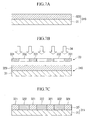
- ultraviolet light 34 is irradiated onto the transparent conductive film 323.
- a mask 33 with a non-transmissive portion 331 and a transmissive portion 332 is applied to the transparent conductive film 323, and the ultraviolet light 34 is irradiated through the mask 33 (ultraviolet irradiation step).
- the ultraviolet light 34 has a wavelength of, for example, 230 to 280 nm.
- the intensity of the ultraviolet light 34 is preferably 100 mW or more, and the irradiation time thereof is preferably one minute or more.
- the portion irradiated with the ultraviolet light 34 through the transmissive portion 332 undergoes a decrease in conductivity to form the second region 322 as the high-resistance region.
- the portion shielded from the ultraviolet light 34 by the non-transmissive portion 331 does not undergo a decrease in conductivity and thus form the first region 321, which is the low-resistance region.
- FIG. 8 shows one example of chronological change in surface resistance value of the irradiated portion and the non-irradiated portion. As shown in the figure, the non-irradiated portion has a small change in resistance value, while the resistance value of the irradiated portion rises gradually due to irradiation of the ultraviolet light 34.
- the regions 321 and 322 are substantially rectangular in cross-section.
- the transparent conductive circuit substrate 311 shown in FIG. 6 is obtained.
- a transparent conductive film 32 is provided with the first region 321 (low-resistance region) as the wiring portion 320 and the second region 322 (high-resistance region).
- the conductivity of the wiring portion 320 can be made favorable. Furthermore, the wiring portion 320 with a narrow width can be formed with ease.
- the first region 321 and the second region 322 are both formed in the transparent conductive film 32, which leads to a simple configuration. This enables the manufacture thereof to be easy and low in cost.
- the shape of the first region 321 can be formed accurately.
- the transparent conductive film 32 can be thinly formed without reducing the conductivity of the first region 321.
- the first region 321 and the second region 322 are both formed in the transparent conductive film 32, thereby making the surface of the transparent conductive circuit substrate 311 flat. This makes lamination of the wiring portion 320 easy compared with the case of the prior-art product in which the wiring portion is formed by printing.
- the ultraviolet light 34 is irradiated onto a portion of the transparent conductive film 323 to form the second region 322 from the irradiated region and form the first region 321 from the non-irradiated region. Therefore, the first region 321 and the second region 322 can be formed by easy operations.
- a dry process can be adopted to the above film formation step and ultraviolet irradiation step. Therefore, the yield can be increased. Furthermore, the amount of emission of waste fluid can be suppressed, which is preferable also from the viewpoint of environmental conservation.
- the bond energy in the molecule is in the energy range of ultraviolet light. Therefore, the bond is radically cleaved by the irradiation of ultraviolet light. As a result, the conductivity is decreased.
- a curing step of drying and curing the transparent conductive film 323 be performed prior to the ultraviolet irradiation step.
- the temperature condition in this step can be set to, for example, from 50 to 130°C.
- the treatment time is preferably from 1 to 10 minutes.
- Curing the transparent conductive film 323 allows the mask 33 to abut the transparent conductive film 32 in the ultraviolet irradiation step.
- the regions 321 and 322 corresponding accurately to the shapes of the non-transmissive portion 331 and the transmissive portion 332 can be formed.
- a display apparatus such as an organic EL apparatus can be listed in which a light-emission element (not shown) is provided on the transparent conductive circuit substrate 311.
- the thickness of the transparent conductive film 32 can be made uniform, thereby making the light transmittance of the transparent conductive film 32 uniform.
- the transparent conductive circuit substrate 311 is used for a display apparatus such as an organic EL apparatus, the display properties thereof can be improved.
- a touch panel can be listed in which a conductive layer (not shown) is provided above the transparent conductive circuit substrate 311 spaced apart such that the conductive layer is brought into contact with the wiring portion 320 by depression from above.
- a transparent conductive film 323 made of transparent conductive ink was formed including polythiophene-based conductive polymers (Denatron #5002LA manufactured by Nagase & Co. Ltd.) by dip coating to obtain a conductive substrate 310.
- the transparent conductive film 323 was dried at a temperature of 80°C for two minutes to be cured.
- Ultraviolet light 34 was irradiated onto the transparent conductive film 323 through a chrome mask 33 having a non-transmissive portion 331 with a width of 10 mm to obtain a transparent conductive circuit substrate 311 having a first region 321 (wiring portion 320) with a width of 10 mm and a second region 322.
- the irradiation intensity of the ultraviolet light 14 was 500 mW/cm 2 .
- the irradiation time thereof was 15 minutes.
- the transparent conductive circuit substrate 311 was evaluated for its appearance, surface resistance, and light transmittance. The evaluation results are shown in Table 1.
- a paste including polythiophene-based polymers was used to form a wiring portion on a base material by screen printing to obtain a transparent conductive circuit substrate.
- Other conditions were in conformance with those of Example 3-1.
- the transparent conductive circuit substrate was evaluated for its appearance, surface resistance, and light transmittance. The evaluation results are shown in Table 4.
- Table 4 Example 3-1 Comparative Ex. 3-1 Base material PET film PET film Conductive substance Polythiophene-based conductive polymer Polythiophene-based conductive polymer Method for forming wiring portion Ultraviolet irradiation Screen printing Appearance of wiring portion Continuous Discontinuous due to bubbles Surface resistance 800 ⁇ / ⁇ 5 ⁇ 10 3 ⁇ / ⁇ Light transmittance 75% 62% Width of wiring portion 10 mm 10mm
- Example 3-1 in which the first region 321 and the second region 322 were formed in the transparent conductive film 32 and the first region 321 was used as the wiring portion 320, experienced less shape deformation in the wiring portion 320 and consequently favorable conductivity compared with Comparative Example 3-1, in which the wiring portion was formed by the printing method.
- Example 3-1 was capable of obtaining a result superior to that of Comparative Example 3-1 also in terms of light transmittance.
- a conductive substrate 310 was manufactured in the similar manner as that of Example 3-1.
- Ultraviolet light 34 was irradiated through a chrome mask 33 having a non-transmissive portion 331 with a width of 5 mm and a transmissive portion 332 with a width of 5 mm to obtain a transparent conductive circuit substrate 311 having a first region 321 (wiring portion 320) with a width of 5 mm and a second region 322 with a width of 5 mm.
- the irradiation intensity of the ultraviolet light 34 was 500 mW/cm 2 .
- the irradiation time thereof was 15 minutes. Other conditions were in conformance with those of Example 3-1.
- the first region 321 as the non-irradiated region and the second region 322 as the irradiated region were evaluated for their appearance, surface resistance, and insulativity between neighboring parts of the wiring portion 320.
- the evaluation results are shown in Table 2.
- a transparent conductive circuit substrate 311 was manufactured in a similar manner to Example 3-2, the exception being that the time for the ultraviolet irradiation was set to three minutes, five minutes, or ten minutes.
- the evaluation results are shown in Table 5.
- Table 5 Example 3-2 Comparative Example 3-2 Comparative Example 3-3 Comparative Example 3-4 Base material PET film PET film PET film PET film Conductive substance Polythiophene-based conductive polymer Polythiophene-based conductive polymer Polythiophene-based conductive polymer Polythiophene-based conductive polymer Polythiophene-based conductive polymer Method for forming wiring portion Ultraviolet irradiation Ultraviolet irradiation Ultraviolet irradiation Ultraviolet irradiation Irradiation time 15 min. 3 min. 5 min. 10 min.
- Table 5 shows that the longer the irradiation time is, the higher the resistance value of the irradiated portion is and that a transparent conductive circuit substrate with a sufficient insulation between parts of the wiring portion was obtained by 15 minutes of irradiation.
- the electronic device manufacturing method of the present invention can provide the transparent conductive film with favorable conductivity. Therefore, it is applicable to precise electronic devices such as organic EL apparatuses, touch panels, and integrated circuits.
Landscapes
- Physics & Mathematics (AREA)
- Engineering & Computer Science (AREA)
- General Physics & Mathematics (AREA)
- Manufacturing & Machinery (AREA)
- Spectroscopy & Molecular Physics (AREA)
- Architecture (AREA)
- Structural Engineering (AREA)
- Non-Insulated Conductors (AREA)
- Manufacturing Of Electric Cables (AREA)
- Parts Printed On Printed Circuit Boards (AREA)
Abstract
Description
- The present invention relates to an electronic device such as an organic electroluminescence apparatus (organic EL apparatus) and a touch panel, to a transparent conductive circuit substrate used for the same, and to a device manufacturing method.
- Priority is claimed on
Japanese Patent Application No. 2004-376275 Japanese Patent Application No. 2004-376276 Japanese Patent Application No. 2004-376277, filed on December 27, 2004 - Conventionally, electronic devices using a transparent conductive circuit substrate furnished with a wiring portion made of a transparent conductive film including conductive polymers are in wide use (see, for example, Patent Document 1).
- The above-mentioned wiring portion is typically formed by printing a paste in which conductive polymers are dispersed in water onto a substrate by the screen printing or ink jet printing such that the paste is in a predetermined shape (for example, in a linear shape).
Patent Document 1:Japanese Unexamined Patent Application, First Publication No. 2002-222056 - However, when the wiring portion is formed by use of conductive polymers, the wiring portion sometimes becomes imperfect in shape. This is because the wiring portion is deformed by the mixture of bubble into the paste, oozing of the paste on the substrate, or repulsion of the paste by the substrate, due to properties (viscosity, etc.) of the paste.
- When the wiring portion has become imperfect in shape, the electrical resistance value of the wiring portion sometimes becomes unstable.
- It is possible to adjust the shape of the wiring portion by stackingly coating a paste on top of the coated paste. In this case, however, the wiring portion becomes thick, thereby reducing its transparency. Moreover, this has posed a problem that it is disadvantageous in terms of cost because more manufacturing steps are required.
- The present invention has been achieved in view of the above circumstances, and has an object to provide an electronic device that has a transparent conductive film using conductive polymers with favorable conductivity and light transmittance and that is capable of reducing its cost, a transparent conductive circuit substrate used therefor, and an electronic device manufacturing method.
- An electronic device manufacturing method according to a first aspect of the present invention is a manufacturing method for an electronic device provided with a transparent conductive film including conductive polymers on a base material. The transparent conductive film has a first region and a second region, adjacent to the first region, having an electrical resistance value higher than that of the first region. The method includes a film formation step of forming the transparent conductive film including conductive polymers on the base material; and an ultraviolet light irradiation step of irradiating ultraviolet light onto a part of the transparent conductive film to form the second region from an irradiated portion and form the first region from a non-irradiated portion. The ultraviolet light in the ultraviolet light irradiation step including a wavelength that exhibits an absorbance in an absorption spectrum of the conductive polymers two or more times higher than that of a background.
- An electronic device manufacturing method according to a second aspect of the present invention is the above-mentioned electronic device manufacturing method, having a curing step of drying and curing the transparent conductive film prior to the ultraviolet irradiation step.
- An electronic device according to a third aspect of the present invention is provided with a transparent conductive film including conductive polymers and a radical polymerization initiator on a base material. The transparent conductive film has a first region and a second region, adjacent to the first region, having an electrical resistance value higher than that of the first region.
- An electronic device according to a fourth aspect of the present invention is the above-mentioned electronic device, in which the first region is a wiring portion used for a circuit.
- An electronic device according to a fifth aspect of the present invention is the above-mentioned electronic device, in which an electronic resistance value of the second region is 104 or more times that of the first region.
- A transparent conductive circuit substrate according to a sixth aspect of the present invention is provided with a transparent conductive film including conductive polymers and a radical polymerization initiator on a base material, in which the transparent conductive film has a first region and a second region, adjacent to the first region, having an electrical resistance value higher than that of the first region, and the first region is a wiring portion used for a circuit.
- An electronic device manufacturing method according to a seventh aspect of the present invention is a manufacturing method for an electronic device provided with a transparent conductive film including conductive polymers and a radical polymerization initiator on a base material. The transparent conductive film has a first region and a second region, adjacent to the first region, having an electrical resistance value higher than that of the first region, in which the method includes a film formation step of forming the transparent conductive film including conductive polymers on the base material, and an ultraviolet light irradiation step of irradiating ultraviolet light onto a part of the transparent conductive film to form the second region from an irradiated portion and form the first region from a non-irradiated portion.
- An electronic device manufacturing method according to an eighth aspect of the present invention is the above-mentioned electronic device manufacturing method, having a curing step of drying and curing the transparent conductive film prior to the ultraviolet irradiation step.
- An electronic device according to a ninth aspect of the present invention is provided with a transparent conductive film including polythiophene-based conductive polymers on a base material. The transparent conductive film has a first region and a second region, adjacent to the first region, having an electrical resistance value higher than that of the first region.
- An electronic device according to a tenth aspect of the present invention is the above-mentioned electronic device, in which the first region is a wiring portion used for a circuit.
- An electronic device according to an eleventh aspect of the present invention is the above-mentioned electronic device, in which an electronic resistance value of the second region is 104 or more times that of the first region.
- A transparent conductive circuit substrate according to a twelfth aspect of the present invention is provided with a transparent conductive film including polythiophene-based conductive polymers on a base material, in which the transparent conductive film has a first region and a second region, adjacent to the first region, having an electrical resistance value higher than that of the first region, and the first region is a wiring portion constituting a circuit.
- An electronic device manufacturing method according to a thirteenth aspect of the present invention is a manufacturing method for an electronic device provided with a transparent conductive film including polythiophene-based conductive polymers on a base material. The transparent conductive film has a first region and a second region, adjacent to the first region, having an electrical resistance value higher than that of the first region, in which the method includes a film formation step of forming the transparent conductive film including polythiophene-based conductive polymers on the base material, and an ultraviolet light irradiation step of irradiating ultraviolet light onto a part of the transparent conductive film to form the second region from an irradiated portion and form the first region from a non-irradiated portion.
- An electronic device manufacturing method according to a fourteenth aspect of the present invention is the above-mentioned device manufacturing method, having a curing step of drying and curing the transparent conductive film prior to the ultraviolet irradiation step.
- According to the first and second aspects of the present invention, the ultraviolet light in the ultraviolet light irradiation step includes a wavelength that exhibits an absorbance in an absorption spectrum of the conductive polymers two or more times higher than that of the background. Thus, the conductivity of the irradiated portion can be effectively reduced.
- As a result, the first region and the second region are allowed to be formed by short-time ultraviolet light irradiation. Therefore, manufacturing efficiency can be improved and manufacturing costs can be reduced.
- Furthermore, since the first region and the second region are allowed to be formed by short-time ultraviolet light irradiation, the conductivity of the first region as a non-irradiated portion can be prevented from reducing due to ultraviolet light.
- Therefore, the first region with favorable conductivity can be formed.
- Moreover, the first region and the second region are formed in the transparent conductive film by an ultraviolet light irradiation. Thus, formation failure of the wiring portion due to oozing of the paste or the like is less likely to occur compared with the case of the prior-art product in which the wiring portion is formed by printing, thereby allowing formation of the first region with an accurate shape.
- Therefore, the conductivity of the first region (wiring portion) can be made favorable.
- Furthermore, since the shape of the first region can be formed accurately, the transparent conductive film can be thinly formed without reducing the conductivity of the first region.
- Therefore, light transmittance of the transparent conductive film can be increased.
- According to the third to eighth aspects of the present invention, the transparent conductive film includes a radical polymerization initiator. Therefore, reactivity of the conductive polymers to ultraviolet light is high, which prompts a reaction of reducing conductivity.
- As a result, the first region and the second region are allowed to be formed by short-time ultraviolet light irradiation. Thus, manufacturing efficiency can be improved and manufacturing costs can be reduced.
- Moreover, since the first region and the second region are allowed to be formed by short-time ultraviolet light irradiation, the first region as the non-irradiated portion can be prevented from deteriorating due to ultraviolet light.
- Therefore, the conductivity of the first region (wiring portion) can be made favorable.
- Furthermore, since the radical polymerization initiator can improve reactivity of the conductive polymers to ultraviolet light, a reaction of reducing conductivity can be prompted even in a deep region of the transparent conductive film.
- As a result, even when the transparent conductive film is thickly formed, the first region can be formed with an accurate shape (for example, a cross sectional rectangular shape).
- Moreover, formation failure of the wiring portion due to oozing of the paste or the like is less likely to occur compared with the case of the prior-art product in which the wiring portion is formed by printing, thereby allowing formation of the first region with an accurate shape.
- As a result, the transparent conductive film can be thinly formed without reducing the conductivity of the first region.
- Therefore, light transmittance of the transparent conductive film can be increased.
- According to the ninth to fourteenth aspects of the present invention, the transparent conductive film is provided with the first region (low-resistance region) and the second region (high-resistance region). Thus, formation failure of the wiring portion due to oozing of the paste or the like is less likely to occur compared with the case of the prior-art product in which the wiring portion is formed by printing, thereby allowing formation of the first region with an accurate shape. Therefore, the conductivity of the first region (wiring portion) can be made favorable.
- Moreover, the first region and the second region are both formed in the transparent conductive film, which leads to a simple configuration. This enables the manufacture thereof to be easy and low in cost.
- Furthermore, the shape of the first region can be formed accurately. Thus, the transparent conductive film can be thinly formed without reducing the conductivity of the first region.
- Therefore, light transmittance of the transparent conductive film can be increased.
-
- FIG. 1 is a schematic block diagram showing a transparent conductive circuit substrate obtained by an electronic device manufacturing method according to a first embodiment of the present invention.
- FIG. 2A is a drawing illustrating a manufacturing method for the transparent conductive circuit substrate shown in FIG. 1 step-by-step.
- FIG. 2B is a drawing illustrating a manufacturing method for the transparent conductive circuit substrate shown in FIG. 1 step-by-step.
- FIG. 2C is a drawing illustrating a manufacturing method for the transparent conductive circuit substrate shown in FIG. 1 step-by-step.
- FIG. 3 is a graph showing an ultraviolet absorption spectrum of the transparent conductive film.
- FIG. 4 is a schematic block diagram showing a transparent conductive circuit substrate usable in an electronic device according to a second embodiment of the present invention.
- FIG. 5A is a drawing illustrating a manufacturing method for the transparent conductive circuit substrate shown in FIG. 4 step-by-step.
- FIG. 5B is a drawing illustrating a manufacturing method for the transparent conductive circuit substrate shown in FIG. 4 step-by-step.
- FIG. 5C is a drawing illustrating a manufacturing method for the transparent conductive circuit substrate shown in FIG. 4 step-by-step.
- FIG. 6 is a schematic block diagram showing a transparent conductive circuit substrate usable in an electronic device according to a third embodiment of the present invention.
- FIG. 7A is a drawing illustrating a manufacturing method for the transparent conductive circuit substrate shown in FIG. 6 step-by-step.
- FIG. 7B is a drawing illustrating a manufacturing method for the transparent conductive circuit substrate shown in FIG. 6 step-by-step.
- FIG. 7C is a drawing illustrating a manufacturing method for the transparent conductive circuit substrate shown in FIG. 6 step-by-step.
- FIG. 8 is a graph showing the change in resistance value of the transparent conductive film by ultraviolet irradiation.
- 11: base material; 12: transparent conductive film; 13: mask; 14: ultraviolet light; 110: conductive substrate; 111: transparent conductive circuit substrate; 120: wiring portion; 121: first region; 122: second region; 131: non-transmissive portion; 132: transmissive portion; 21: base material; 22: transparent conductive film; 23: mask; 24: ultraviolet light; 210: conductive substrate; 211: transparent conductive circuit substrate; 220: wiring portion; 221: first region; 222: second region; 231: non-transmissive portion; 232: transmissive portion; 31: base material; 32: transparent conductive film; 33: mask; 34: ultraviolet light; 310: conductive substrate; 311: transparent conductive circuit substrate; 320: wiring portion; 321: first region; 322: second region; 331: non-transmissive portion; 332: transmissive portion
- FIG. 1 is a cross-sectional view showing a part of one example of a transparent conductive circuit substrate obtained by an electronic device manufacturing method according to a first embodiment of the present invention.
- The transparent
conductive circuit substrate 111 is furnished with a transparentconductive film 12 including conductive polymers on abase material 11. - The
base material 11 is made of a transparent material, for example, polyethylene terephthalate (PET), and is formed in a plate or film shape. - The transparent
conductive film 12 is made of conductive polymers with a characteristic in which the electrical resistance value is increased by ultraviolet irradiation. - The transparent
conductive film 12 has afirst region 121 and asecond region 122 formed adjacent to thefirst region 121. - The
first region 121 is a low-resistance region with a comparatively low electrical resistance value. Thefirst region 121 can have an electrical resistance value (surface resistance) of, for example, 103 Ω/□ or less. - The
first region 121 is awiring portion 120 that is used for a transparent conductive circuit. - The
first region 121 is not particularly limited with respect to its shape. It may have a linear shape with a predetermined width. - The
second region 122 is a high-resistance region with an electrical resistance higher than that of thefirst region 121. - It is preferable that the
second region 122 have an electrical resistance value (surface resistance) 104 or more times (preferably 105 or more times) than that of thefirst region 121. Specifically, it can have an electrical resistance value of 108Ω/□ or more. - Making the electrical resistance value of the
second region 122 104 or more times that of thefirst region 121 can improve the insulativity between neighboring parts of thewiring portion 120, and make the conductivity of thewiring portion 120 favorable. - As for the conductive polymer, a polythiophene-based conductive polymer is preferable.
- As for the polythiophene-based conductive polymer, for example, one formed with a cation structure by doping an undoped polymer having a principal chain of a polythiophene-based polymer shown in Formula (1) with a halogen such as iodine or other oxidant to partially oxidize the polymer can be used.

- In Formula (1), groups R1 and R2 are independently selectable. The following can be exemplified: a hydrogen atom; a halogen atom such as fluorine, chlorine, bromine, or iodine; a cyano group; a straight-chain alkyl group such as methyl, ethyl, propyl, butyl (n-butyl), pentyl (n-pentyl), hexyl, octyl, dodecyl, hexadecyl, or octadecyl; a branched-chain alkyl group such as isopropyl, isobutyl, sec-butyl, tert-butyl, isopentyl, or neopentyl; an alkoxy group with a straight- or branched-chain such as methoxy, ethoxy, propoxy, isopropoxy, butoxy, isobutoxy, sec-butoxy, or tert-butoxy; an alkenyl group such as vinyl, propenyl, allyl, butenyl, or oleyl; an alkynyl group such as ethynyl, propynyl, or butynyl; an alkoxyalkyl group such as methoxymethyl, 2-methoxyethyl, 2-ethoxyethyl, and 3-ethoxypropyl; a polyether group such as C2H5O(CH2CH2O)mCH2CH2 group (m is an integer equal to or more than one) or CH3O(CH2CH2O)mCH2CH2 group (m is an integer equal to or more than one); and a halogen-substituted derivative, such as a fluoromethyl group, in which the above substituent is substituted with fluorine or the like.
- It is preferable that the conductive polymer include a π-conjugated bond in the principal chain thereof.
- As for the polythiophene-based polymer, 3,4-ethylenedioxythiophene) (PEDOT) is preferable. Especially, PEDOT-PSS, which is PEDOT doped with polystyrene sulfonate (PSS), is preferable.
- A conductive film made of PEDOT-PSS can be produced, for example, as follows:
- Fe(III)tris-p-toluenesulfonate solution and 1-butanol solution of imidazole are added to 3,4-ethylenedioxythiophene monomer. The mixture is coated on a base material. After the base material is heated and dried, the base material is rinsed in methanol to remove Fe(II)bis-p-toluenesulfonate.
- As for commercially available products usable as polythiophene-based polymers, Baytron P manufactured by H.C. Starck-V TECH Ltd., Denatron #5002LA manufactured by Nagase & Co. Ltd., and Orgacon S300 manufactured by Agfa-Gevaert Group can be listed.
- Next, a manufacturing method for the transparent
conductive circuit substrate 111 according to the first embodiment of the present invention will be described. - As shown in FIG. 2A, a transparent
conductive film 123 with a substantially uniform thickness is formed on abase material 11 by coating raw material liquid including conductive polymers over the entirety of thebase material 11 or by other methods to obtain a conductive substrate 110 (film formation step). - Coating of the raw material liquid can be performed also by dip coating, spin coating, bar coating, or the like. Note that the transparent
conductive film 123 may be formed by a method other than coating. - FIG. 3 shows one example of an ultraviolet absorption spectrum of a conductive polymer usable for the transparent
conductive film 123. As shown in the figure, the absorbance of the conductive polymer is maximum (local maximum) at a wavelength of about 240 nm, and is substantially the steady-state value (background) in the range of 500 nm or higher. - As shown in FIG. 2B,
ultraviolet light 14 is irradiated onto the transparentconductive film 123. - At this time, a
mask 13 with anon-transmissive portion 131 and atransmissive portion 132 is applied to the transparentconductive film 123, and theultraviolet light 14 is irradiated through the mask 13 (ultraviolet irradiation step). - As for the
ultraviolet light 14, one that includes a wavelength showing an absorbance in its absorption spectrum two or more times (preferably 2.5 or more times) higher than that of a background is used. - In the example shown in FIG. 3, the absorbance of the background is 0.18. Therefore, the absorbance corresponding to twice that of the background is 0.36. The lower limit value λ1 of the wavelength that shows the absorbance corresponding to 0.36 or more is 225 nm and the upper limit value λ2 thereof is 300 nm.
- That is, as for the
ultraviolet light 14, one including a wavelength of 225 to 300 nm is used. Moreover, a wavelength that exhibits an absorbance 2.5 or more times higher than that of the background is 230 to 280 nm. - The intensity of the
ultraviolet light 14 is preferably 100 mW or more, and the irradiation time thereof is preferably 30 seconds or more. - As shown in FIG. 2C, the portion irradiated with the
ultraviolet light 14 through the transmissive portion 132 (irradiated portion) undergoes a decrease in conductivity to form thesecond region 122 as the high-resistance region. - The portion shielded from the
ultraviolet light 14 by the non-transmissive portion 131 (non-irradiated portion) does not undergo a decrease in conductivity and thus forms thefirst region 121, which is the low-resistance region. - When the irradiation direction of the
ultraviolet light 14 is substantially perpendicular to the transparentconductive film 123, theregions - By the above operations, the transparent
conductive circuit substrate 111 shown in FIG. 1 is obtained. - In the above manufacturing method, the
ultraviolet light 14 irradiated onto the transparentconductive film 123 in the ultraviolet light irradiation step includes a wavelength that shows the above-mentioned absorbance two or more times higher than that of the background. Therefore, the conductivity of the irradiated portion can be efficiently reduced. - As a result, the
first region 121 and thesecond region 122 are allowed to be formed by short-time ultraviolet light irradiation. Thus, manufacturing efficiency can be improved and manufacturing costs can be reduced. - Moreover, since the
first region 121 and thesecond region 122 are allowed to be formed by a short-time irradiation of ultraviolet light, the conductivity of thefirst region 121 as the non-irradiated portion can be prevented from deteriorating due toultraviolet light 14. Therefore, the conductivity of thewiring portion 120 can be made favorable. - Moreover, the
first region 121 and thesecond region 122 are formed in the transparentconductive film 12 by ultraviolet light irradiation. Thus, formation failure of the wiring portion due to oozing of the paste or the like is less likely to occur compared with the case of the prior-art product in which the wiring portion is formed by printing, thereby allowing formation of thefirst region 121 with an accurate shape. - Therefore, the conductivity of the
wiring portion 120 can be made favorable. Moreover, thewiring portion 120 with a narrow width can be formed with ease. - Furthermore, since the shape of the
first region 121 can be formed accurately, the transparentconductive film 12 can be thinly formed without reducing the conductivity of thefirst region 121. - Therefore, light transmittance of the transparent
conductive film 12 can be increased. - The reason why the transparent
conductive film 123 undergoes reduction in conductivity in the region irradiated with theultraviolet light 14 is not clear. However, it is possible to presume the following: - In the above conductive polymer, the bond energy in the molecule is in the energy range of ultraviolet light. Therefore, the bond is radically cleaved by the irradiation of ultraviolet light. As a result, the conductivity is decreased.
- As for the above polymer, one having a maximum ultraviolet absorption wavelength of 380 nm or less, preferably 330 nm or less is preferable.
- When a conductive polymer with the maximum absorption wavelength within this range is used, the ultraviolet light that satisfies the aforementioned condition comes to have a comparatively short wavelength. Therefore, the ultraviolet light is highly likely to travel in a straight line and does not spread when irradiated through the mask. As a result, the
wiring portion 120 with an accurate shape (for example, cross-sectional rectangular shape) can be formed. - It is preferable that the maximum ultraviolet absorption wavelength of the conductive polymer be 220 nm or more.
- When a conductive polymer with the maximum absorption wavelength within this range is used, ultraviolet light is likely to reach a deep portion of the transparent conductive film.
- In the present invention, it is preferable that prior to the ultraviolet irradiation step, a curing step of drying and curing the transparent
conductive film 123 be performed. - The temperature condition in this step can be set to, for example, from 50 to 130 ° C. The treatment time is preferably from 1 to 10 minutes.
- Curing the transparent
conductive film 123 allows themask 13 to abut the transparentconductive film 12 in the ultraviolet irradiation step. - Therefore, the
regions non-transmissive portion 131 and thetransmissive portion 132 can be formed. - As for an electronic device to which the transparent
conductive circuit substrate 111 is applied, a display apparatus such as an organic EL apparatus can be listed in which a light-emission element (not shown) is provided on the transparentconductive circuit substrate 111. - In the transparent
conductive circuit substrate 111, the thickness of the transparentconductive film 12 can be made uniform, thereby making the light transmittance of the transparentconductive film 12 uniform. - Therefore, when the transparent
conductive circuit substrate 111 is used for a display apparatus such as an organic EL apparatus, the display properties thereof can be improved. - As another example of an electronic device, a touch panel can be listed in which a conductive layer (not shown) is provided above the transparent
conductive circuit substrate 111 spaced apart such that the conductive layer is brought into contact with thewiring portion 120 by depression from above. - On a
base material 11 made of a PET film (Lumirror S10 manufactured by Toray Industries, Inc.) with a length of 15 cm, a width of 15 cm, and a thickness of 188 µm, a transparentconductive film 123 made of transparent conductive ink was formed including polythiophene-based conductive polymers (Denatron #5002LA manufactured by Nagase & Co. Ltd.) by dip coating to obtain aconductive substrate 110. The transparentconductive film 123 was dried at a temperature of 80°C for two minutes to be cured. - As for the conductive polymer, one that shows the ultraviolet absorption spectrum shown in FIG. 3 was used.
-
Ultraviolet light 14 was irradiated onto the transparentconductive film 123 through amask 13 having anon-transmissive portion 131 with a width of 10 mm to obtain a transparentconductive circuit substrate 111 having a first region 121 (wiring portion 120) with a width of 10 mm and asecond region 122. - The
ultraviolet light 14 was irradiated in a condition that light with up to a predetermined wavelength was cut off by use of a cut filter. The irradiation intensity of theultraviolet light 14 was 500 mW/cm2. - The results of the chronological measurements of the surface resistance of the portions irradiated with the
ultraviolet light 14 are shown in Table 1. - The surface resistances of the
first region 121 for all the examples were 800 Ω/□. - A transparent
conductive circuit substrate 111 was manufactured in a similar manner to Example 1-1 with the exception being that a cut filter with a different cutoff wavelength was used. - The results of the chronological measurements of the surface resistance of the portion irradiated with the
ultraviolet light 14 are shown in Table 1. - The surface resistance of the
first region 121 was 800 Ω/□.Table 1 Example 1-1 Example 1-2 Example 1-3 Comp. Ex. 1-1 Wavelength of light cut off by cut filter 220 nm or less 260 nm or less 290 nm or less 330 nm or less Surface resistance (Ω/□) At start of irradiation 800 800 800 800 after 10 min. 1.0×10⁸↑ 1.0×10⁸↑ 7.0×10⁵ 1.0×10⁵ after 15 min. 1.0×10⁸↑ 1.0×10⁸↑ 5.0×10⁶ 1.0×10⁶ after 20 min. 1.0×10⁸↑ 1.0×10⁸↑ 1.0×10⁸↑ 1.0×10⁸↑ ("1.0×10⁸↑ Ω/□" means that the measured value exceeded a measurement limit value of 1.0×10⁸ Ω/□.) - Table 1 shows that the resistance value in the irradiated region rose in a short period of time in Example 1-1 using ultraviolet light with a wavelength over 220 nm, Example 1-2 using ultraviolet light with a wavelength over 260 nm, and Example 1-3 using ultraviolet light with a wavelength over 290 nm.
- In contrast to this, it took a comparatively long time for the resistance value to rise in Comparative Example using ultraviolet light with a wavelength over 330 nm.
- These results reveal that irradiation of ultraviolet light with a wavelength (225 to 300 nm) that shows absorbance two or more times higher than that of the background can form the
first region 121 and thesecond region 122 in a short period of time. - FIG. 4 is a cross-sectional view showing a part of one example of a transparent conductive circuit substrate according to a second embodiment of the present invention.
- The transparent
conductive circuit substrate 211 is furnished with a transparentconductive film 22 including conductive polymers on abase material 21. - The
base material 21 is made of a transparent material, for example, polyethylene terephthalate (PET), and is formed in a plate or film shape. - The transparent
conductive film 22 has afirst region 221 and asecond region 222 formed adjacent to thefirst region 221. - The transparent
conductive film 22 is made of conductive polymers with a characteristic in which the electrical resistance value is increased by irradiation of ultraviolet light. - The
first region 221 is a low-resistance region with a comparatively low electrical resistance value. Thefirst region 221 may have an electrical resistance value (surface resistance) of, for example, 103 Ω/□ or less. - The
first region 221 is awiring portion 220 that is used for a transparent conductive circuit. - The
first region 221 is not particularly limited with respect to its shape. It may have a linear shape with a predetermined width. - The
second region 222 is a high-resistance region with an electrical resistance higher than that of thefirst region 221. - It is preferable that the
second region 222 have an electrical resistance value (surface resistance) 104 or more times (preferably 105 or more times) than that of thefirst region 221. Specifically, it can have an electrical resistance value of 108 Ω/□ or more. - Making the electrical resistance value of the
second region 222 104 or more times that of thefirst region 221 can improve the insulativity between neighboring parts of thewiring portion 220, and make the conductivity of thewiring portion 220 favorable. - As for the conductive polymer, a polythiophene-based conductive polymer is preferable.
- As for the polythiophene-based conductive polymer, for example, one formed with a cation structure by doping an undoped polymer having a principal chain of a polythiophene-based polymer shown in Formula (1) with a halogen such as iodine or other oxidant to partially oxidize the polymer can be used.

- In Formula (1), groups R1 and R2 are independently selectable. The following can be exemplified: a hydrogen atom; a halogen atom such as fluorine, chlorine, bromine, or iodine; a cyano group; a straight-chain alkyl group such as methyl, ethyl, propyl, butyl (n-butyl), pentyl (n-pentyl), hexyl, octyl, dodecyl, hexadecyl, or octadecyl; a branched-chain alkyl group such as isopropyl, isobutyl, sec-butyl, tert-butyl, isopentyl, or neopentyl; an alkoxy group with a straight- or branched-chain such as methoxy, ethoxy, propoxy, isopropoxy, butoxy, isobutoxy, sec-butoxy, or tert-butoxy; an alkenyl group such as vinyl, propenyl, allyl, butenyl, or oleyl; an alkynyl group such as ethynyl, propynyl, or butynyl; an alkoxyalkyl group such as methoxymethyl, 2-methoxyethyl, 2-ethoxyethyl, and 3-ethoxypropyl; a polyether group such as C2H5O(CH2CH2O)mCH2CH2 group (m is an integer equal to or more than one) or CH3O(CH2CH2O)mCH2CH2 group (m is an integer equal to or more than one); and a halogen-substituted derivative, such as a fluoromethyl group, in which the above substituent is substituted with fluorine or the like.
- It is preferable that the conductive polymer include a π-conjugated bond in the principal chain thereof.
- As for the polythiophene-based polymer, 3,4-ethylenedioxythiophene) (PEDOT) is preferable. Especially, PEDOT-PSS, which is PEDOT doped with polystyrene sulfonate (PSS), is preferable.
- A conductive film made of PEDOT-PSS can be produced, for example, as follows:
- Fe(III)tris-p-toluenesulfonate solution and 1-butanol solution of imidazole are added to 3,4-ethylenedioxythiophene monomer. The mixture is coated on a base material. After the base material is heated and dried, the base material is rinsed in methanol to remove Fe(II)bis-p-toluenesulfonate.
- As for commercially available products usable as polythiophene-based polymers, Baytron P manufactured by H.C. Starck-V TECH Ltd., Denatron #5002LA manufactured by Nagase & Co. Ltd., and Orgacon S300 manufactured by Agfa-Gevaert Group can be listed.
- A radical polymerization initiator is added to the transparent
conductive film 22. - Radical polymerization initiators are generally used to start radical polymerization. They have a function to generate energy such as light to start radical polymerization.
- As for a radical polymerization initiator, an azo compound, an organic peroxide, and an inorganic peroxide can be listed.
- As for an azo compound, an azoamide-based compound, azobisisobutyronitrile (AIBN), diazoaminobenezene, and the like can be listed.
- As for an organic peroxide, benzoyl peroxide (BPO), diisopropyl peroxydicarbonate, and the like can be listed.
- As for an inorganic peroxide, persulfate, perchlorate, and the like can be listed.
- It is especially preferable that an azoamide-based compound with high water solubility be used.
- It is preferable that the amount of the radical polymerization initiator added be 0.1% by mass or more. Limiting the amount to be added within this range can increase the reaction rate at which the conductivity of the transparent conductive film 2 is reduced by ultraviolet light. The amount to be added is preferably 0.5% by mass or more, and more preferably 1% by mass or more.
- There is a possibility that too large amount of the radical polymerization initiator added will make it unlikely to cause the above-mentioned reaction of reducing conductivity. Therefore, it is preferable that the amount to be added be 10% by mass or less.
- Next, a manufacturing method for the transparent
conductive circuit substrate 211 according to the second embodiment of the present invention will be described. - As shown in FIG. 5A, a transparent
conductive film 223 with a substantially uniform thickness is formed on abase material 21 by coating raw material liquid including conductive polymers over the entirety of thebase material 21 or by other methods to obtain a conductive substrate 210 (film formation step). - Coating of the raw material liquid can be performed also by dip coating, spin coating, bar coating, or the like. Note that the transparent
conductive film 223 may be formed by a method other than coating. - As shown in FIG. 5B,
ultraviolet light 24 is irradiated onto the transparentconductive film 223. - At this time, a
mask 23 with anon-transmissive portion 231 and atransmissive portion 232 is applied to the transparentconductive film 223, and theultraviolet light 24 is irradiated through the mask 23 (ultraviolet irradiation step). - The
ultraviolet light 24 has a wavelength of, for example, from 230 to 280 nm. - The intensity of the
ultraviolet light 24 is preferably 100 mW or more, and the irradiation time thereof is preferably, for example, 30 seconds or more. - As shown in FIG. 5C, the portion irradiated with the
ultraviolet light 24 through the transmissive portion 232 (irradiated portion) undergoes a decrease in conductivity to form thesecond region 222 as the high-resistance region. - The transparent
conductive film 22 includes a radical polymerization initiator. Therefore, it has a high reactivity of the conductive polymers to the ultraviolet light, thus prompting the reaction of reducing conductivity. - As a result, the
first region 221 and thesecond region 222 are allowed to be formed by a short-time ultraviolet irradiation. Thus, manufacturing efficiency can be improved and manufacturing costs can be reduced. - Moreover, since the
first region 221 and thesecond region 222 are allowed to be formed by a short-time ultraviolet irradiation, thefirst region 221 as the non-irradiated portion can be prevented from degrading due to ultraviolet light. - Therefore, the conductivity of the first region 221 (wiring portion 220) can be made favorable.
- The portion shielded from the
ultraviolet light 24 by the non-transmissive portion 231 (non-irradiated portion) does not undergo a decrease in conductivity and thus forms to thefirst region 221, which is the low-resistance region. - When the irradiation direction of the
ultraviolet light 24 is substantially perpendicular to the transparentconductive film 23, theregions - By the above operations, the transparent
conductive circuit substrate 211 shown in FIG. 4 is obtained. - Since the radical polymerization initiator can improve reactivity of the conductive polymers to ultraviolet light in the above transparent
conductive circuit substrate 211, a reaction of reducing conductivity can be prompted even in a deep region of the transparentconductive film 22. - As a result, even when the transparent
conductive film 22 is thickly formed, thefirst region 221 with an accurate shape (for example, a cross sectional rectangular shape) can be formed. - Moreover, formation failure of the wiring portion due to oozing of the paste or the like is less likely to occur compared with the case of the prior-art product in which the wiring portion is formed by printing, thereby allowing formation of the
first region 221 with an accurate shape. - As a result, the transparent
conductive film 22 can be thinly formed without reducing the conductivity of thefirst region 221. - Therefore, light transmittance of the transparent
conductive film 22 can be increased. - In the above manufacturing method, the
ultraviolet light 24 is irradiated onto a portion of the transparentconductive film 223 to form thesecond region 222 from the irradiated region and form thefirst region 221 from the non-irradiated region. Therefore, thefirst region 221 and thesecond region 222 can be formed by easy operations. - A dry process can be adopted to the above film formation step and ultraviolet irradiation step. Therefore, the yield can be increased. Furthermore, the amount of emission of waste fluid can be suppressed, which is preferable also from the viewpoint of environmental conservation.
- The reason why the transparent
conductive film 223 undergoes reduction in conductivity in the region irradiated with theultraviolet light 24 is not clear. However, it is possible to presume the following: - In the above conductive polymer, the bond energy in the molecule is in the energy range of ultraviolet light. Therefore, the bond is radically cleaved by the irradiation of ultraviolet light. As a result, the conductivity is decreased.
- The reason why the reaction of decrease in conductivity can be prompted by use of the radical polymerization initiator can be presumed as follows:
- Radicals generated from the radical polymerization initiator by ultraviolet irradiation increase the reaction rate at which the conductivity of the conductive polymers is decreased.
- In the present invention, a plurality of transparent conductive films may be provided. That is, a transparent conductive circuit substrate provided with two or more transparent conductive films on the base material is included in the scope of the invention.
- The present invention can increase reactivity of conductive polymers to ultraviolet light by use of a radical polymerization initiator. Therefore, when a plurality of transparent conductive films are provided, a first region with an accurate shape can be formed even in transparent conductive film on the bottom layer side.
- In the present invention, it is preferable that prior to the ultraviolet irradiation step, a curing step of drying and curing the transparent
conductive film 223 be performed. - The temperature condition in this step can be set to, for example, from 50 to 130°C. The treatment time is preferably from 1 to 10 minutes.
- Curing the transparent
conductive film 223 allows themask 23 to abut the transparentconductive film 22 in the ultraviolet irradiation step. - Therefore, the
regions non-transmissive portion 231 and thetransmissive portion 232 can be formed. - As for an electronic device to which the transparent
conductive circuit substrate 211 is applied, a display apparatus such as an organic EL apparatus can be listed in which a light-emission element (not shown) is provided on the transparentconductive circuit substrate 211. - In the transparent
conductive circuit substrate 211, the thickness of the transparentconductive film 22 can be made uniform, thereby making the light transmittance of the transparentconductive film 22 uniform. - Therefore, when the transparent
conductive circuit substrate 211 is used for a display apparatus such as an organic EL apparatus, the display properties thereof can be improved. - As another example of an electronic device, a touch panel can be listed in which a conductive layer (not shown) is provided above the transparent
conductive circuit substrate 211 spaced apart such that the conductive layer is brought into contact with thewiring portion 220 by depression from above. - A raw material liquid was prepared by adding a radical polymerization initiator (V-086 manufactured by Wako Pure Chemical Industries, Ltd.) to transparent conductive ink (Denatron #5002LA manufactured by Nagase & Co. Ltd.) including polythiophene-based conductive polymers.
- The raw material liquid was coated by dip coating on a
base material 1 made of a PET film (Lumirror S10 manufactured by Toray Industries, Inc.) with a length of 15 cm, a width of 15 cm, and a thickness of 188 µm to form a transparentconductive film 223, thereby obtaining aconductive substrate 210. The transparentconductive film 223 was dried at a temperature of 80°C for two minutes to be cured. -
Ultraviolet light 24 was irradiated onto the transparentconductive film 223 through achrome mask 23 having a non-transmissive portion with a width of 10 mm to obtain a transparentconductive circuit substrate 211 having a first region 221 (wiring portion 220) with a width of 10 mm and asecond region 222. The irradiation intensity of theultraviolet light 24 was 500 mW/cm2. - The results of the chronological measurements of the surface resistance of the portions irradiated with the
ultraviolet light 24 are shown in Table 3 and Table 4. - The surface resistances of the portions not irradiated with the ultraviolet light were the same in value as those at the start of the irradiation.
Table 2 Example 2-1 Example 2-2 Example 2-3 Example 2-4 Transparent conductive film thickness (µm) 0.4 0.4 0.4 0.4 Amount to be added of polymerization initiator (% by mass) 1 0 0.1 0.5 Surface resistance (Ω/□) At start of irradiation 1200 700 760 900 after 5 min. 3.0×10⁶ 1.0×10³ 7.0×10³ 2.0×10⁵ after 10 min. 1.0×10⁸↑ 1.0×10⁵ 2.0×10⁵ 5.0×10⁶ after 15 min. 1.0×10⁸↑ 3.0×10⁶ 8.0×10⁶ 8.0x×106 ("1.0×10⁸↑ Ω/□" means that the measured value exceeded a measurement limit value of 1.0× 10⁸ Ω/□.) Table 3 Example 2-5 Example 2-6 Example 2-7 Example 2-8 Transparent conductive film thickness (µm) 0.1 0.1 0.1 0.1 Amount to be added of polymerization initiator (% by mass) 1 0 0.1 0.5 Surface resistance (Ω/□) At start of irradiation 2800 2000 2100 2500 after 5 min. 1.0×10⁷ 3.0×10⁴ 7.0×10⁴ 1.0×10⁶ after 10 min. 1.0×10⁸↑ 1.0×x106 8.0×10⁶ 1.0×10⁸↑ after 15 min. 1.0×10⁸↑ 1.0×10⁸↑ 1.0×10⁸↑ 1.0×10⁸↑ ("1 .0×108↑ Ω/□" means that the measured value exceeded a measurement limit value of 1.0×10⁸ Ω/□.) - Table 2 and Table 3 show that addition of the radical polymerization initiator increased the resistance value in a short period of time.
- Furthermore, Table 2 shows that by the addition of the radical polymerization initiator, high resistance values were allowed to be obtained even in the case of thick transparent conductive films.
- These results reveal that using a radical polymerization initiator can form a
first region 221 andsecond region 222 whose ratio of resistance value is high. - FIG. 6 is a cross-sectional view showing a part of one example of a transparent conductive circuit substrate according to a third embodiment of the present invention.
- The transparent
conductive circuit substrate 311 is furnished with a transparentconductive film 32 including conductive polymers on abase material 31. - The
base material 31 is made of a transparent material, for example, polyethylene terephthalate (PET), and is formed in a plate or film shape. - The transparent
conductive film 32 is made of polythiophene-based conductive polymers with a characteristic in which the electrical resistance value is increased by irradiation of ultraviolet light. - The transparent
conductive film 32 has afirst region 321 and a second region formed adjacent to thefirst region 321. - The
first region 321 is a low-resistance region with a comparatively low electrical resistance value. Thefirst region 321 can have an electrical resistance value (surface resistance) of, for example, 103 Ω/□ or less. - The
first region 321 is awiring portion 320 that is used for a transparent conductive circuit. - The
first region 321 is not particularly limited with respect to its shape. It may have a linear shape with a predetermined width. - The
second region 322 is a high-resistance region with an electrical resistance higher than that of thefirst region 321. - It is preferable that the
second region 322 have an electrical resistance value (surface resistance) 104 or more times (preferably 105 or more times) than that of thefirst region 321. Specifically, it can have an electrical resistance value of 108 Ω/□ or more. - Making the electrical resistance value of the
second region 322 104 or more times that of thefirst region 321 can improve the insulativity between neighboring parts of thewiring portion 320, and make the conductivity of thewiring portion 320 favorable. - As for the polythiophene-based conductive polymer, for example, one formed with a cation structure by doping an undoped polymer having a principal chain of a polythiophene-based polymer shown in Formula (1) with a halogen such as iodine or other oxidant to partially oxidize the polymer can be used.

- In Formula (1), groups R1 and R2 are independently selectable. The following can be exemplified: a hydrogen atom; a halogen atom such as fluorine, chlorine, bromine, or iodine; a cyano group; a straight-chain alkyl group such as methyl, ethyl, propyl, butyl (n-butyl), pentyl (n-pentyl), hexyl, octyl, dodecyl, hexadecyl, or octadecyl; a branched-chain alkyl group such as isopropyl, isobutyl, sec-butyl, tert-butyl, isopentyl, or neopentyl; an alkoxy group with a straight- or branched-chain such as methoxy, ethoxy, propoxy, isopropoxy, butoxy, isobutoxy, sec-butoxy, or tert-butoxy; an alkenyl group such as vinyl, propenyl, allyl, butenyl, or oleyl; an alkynyl group such as ethynyl, propynyl, or butynyl; an alkoxyalkyl group such as methoxymethyl, 2-methoxyethyl, 2-ethoxyethyl, and 3-ethoxypropyl; a polyether group such as C2H5O(CH2CH2O)mCH2CH2 group (m is an integer equal to or more than one) or CH3O(CH2CH2O)mCH2CH2 group (m is an integer equal to or more than one a halogen-substituted derivative, such as a fluoromethyl group, in which the above substituent is substituted with fluorine or the like.
- It is preferable that the conductive polymer include a π-conjugated bond in the principal chain thereof.
- As for the polythiophene-based polymer, 3,4-ethylenedioxythiophene) (PEDOT) is preferable. Especially, PEDOT-PSS, which is PEDOT doped with polystyrene sulfonate (PSS), is preferable.
- A conductive film made of PEDOT-PSS can be produced, for example, as follows:
- Fe(III)tris-p-toluenesulfonate solution and 1-butanol solution of imidazole are added to 3,4-ethylenedioxythiophene monomer. The mixture is coated on a base material. After the base material is heated and dried, the base material is rinsed in methanol to remove Fe(II)bis-p-toluenesulfonate.
- As for commercially available products usable as polythiophene-based polymers, Baytron P manufactured by H.C. Starck-V TECH Ltd., Denatron #5002LA manufactured by Nagase & Co. Ltd., and Orgacon S300 manufactured by Agfa-Gevaert Group can be listed.
- Next, a manufacturing method for the transparent
conductive circuit substrate 311 according to the third embodiment of the present invention will be described. - As shown in FIG. 7A, a transparent
conductive film 323 with a substantially uniform thickness is formed on abase material 31 by coating raw material liquid including conductive polymers over the entirety of thebase material 31 or by other methods to obtain a conductive substrate 310 (film formation step). - Coating of the raw material liquid can be performed also by dip coating, spin coating, bar coating, or the like. Note that the transparent
conductive film 323 may be formed by a method other than coating. - As shown in FIG. 7B,
ultraviolet light 34 is irradiated onto the transparentconductive film 323. - At this time, a
mask 33 with anon-transmissive portion 331 and atransmissive portion 332 is applied to the transparentconductive film 323, and theultraviolet light 34 is irradiated through the mask 33 (ultraviolet irradiation step). - The
ultraviolet light 34 has a wavelength of, for example, 230 to 280 nm. - The intensity of the
ultraviolet light 34 is preferably 100 mW or more, and the irradiation time thereof is preferably one minute or more. - As shown in FIG. 7C, the portion irradiated with the
ultraviolet light 34 through the transmissive portion 332 (irradiated portion) undergoes a decrease in conductivity to form thesecond region 322 as the high-resistance region. - The portion shielded from the
ultraviolet light 34 by the non-transmissive portion 331 (non-irradiated portion) does not undergo a decrease in conductivity and thus form thefirst region 321, which is the low-resistance region. - FIG. 8 shows one example of chronological change in surface resistance value of the irradiated portion and the non-irradiated portion. As shown in the figure, the non-irradiated portion has a small change in resistance value, while the resistance value of the irradiated portion rises gradually due to irradiation of the
ultraviolet light 34. - When the irradiation direction of the
ultraviolet light 34 is substantially perpendicular to the transparentconductive film 323, theregions - By the above operations, the transparent
conductive circuit substrate 311 shown in FIG. 6 is obtained. - In the transparent
conductive circuit substrate 311, a transparentconductive film 32 is provided with the first region 321 (low-resistance region) as thewiring portion 320 and the second region 322 (high-resistance region). - As a result, formation failure of the wiring portion due to oozing of the paste or the like is less likely to occur compared with the case of the prior-art product in which the wiring portion is formed by printing, thereby allowing formation of the
first region 321 with an accurate shape. - Therefore, the conductivity of the
wiring portion 320 can be made favorable. Furthermore, thewiring portion 320 with a narrow width can be formed with ease. - In the transparent
conductive circuit substrate 311, thefirst region 321 and thesecond region 322 are both formed in the transparentconductive film 32, which leads to a simple configuration. This enables the manufacture thereof to be easy and low in cost. - Furthermore, the shape of the
first region 321 can be formed accurately. Thus, the transparentconductive film 32 can be thinly formed without reducing the conductivity of thefirst region 321. - Therefore, light transmittance of the transparent
conductive film 32 can be increased. - In the transparent
conductive circuit substrate 311, thefirst region 321 and thesecond region 322 are both formed in the transparentconductive film 32, thereby making the surface of the transparentconductive circuit substrate 311 flat. This makes lamination of thewiring portion 320 easy compared with the case of the prior-art product in which the wiring portion is formed by printing. - In the above manufacturing method, the
ultraviolet light 34 is irradiated onto a portion of the transparentconductive film 323 to form thesecond region 322 from the irradiated region and form thefirst region 321 from the non-irradiated region. Therefore, thefirst region 321 and thesecond region 322 can be formed by easy operations. - A dry process can be adopted to the above film formation step and ultraviolet irradiation step. Therefore, the yield can be increased. Furthermore, the amount of emission of waste fluid can be suppressed, which is preferable also from the viewpoint of environmental conservation.
- The reason why the transparent
conductive film 323 undergoes reduction in conductivity in the region irradiated with theultraviolet light 34 is not clear. However, it is possible to presume the following: - In the polythiophene-based polymer, the bond energy in the molecule is in the energy range of ultraviolet light. Therefore, the bond is radically cleaved by the irradiation of ultraviolet light. As a result, the conductivity is decreased.
- In the present invention, it is preferable that prior to the ultraviolet irradiation step, a curing step of drying and curing the transparent
conductive film 323 be performed. - The temperature condition in this step can be set to, for example, from 50 to 130°C. The treatment time is preferably from 1 to 10 minutes.
- Curing the transparent
conductive film 323 allows themask 33 to abut the transparentconductive film 32 in the ultraviolet irradiation step. - Therefore, the
regions non-transmissive portion 331 and thetransmissive portion 332 can be formed. - As for an electronic device to which the transparent
conductive circuit substrate 311 is applied, a display apparatus such as an organic EL apparatus can be listed in which a light-emission element (not shown) is provided on the transparentconductive circuit substrate 311. - In the transparent
conductive circuit substrate 311, the thickness of the transparentconductive film 32 can be made uniform, thereby making the light transmittance of the transparentconductive film 32 uniform. - Therefore, when the transparent
conductive circuit substrate 311 is used for a display apparatus such as an organic EL apparatus, the display properties thereof can be improved. - As another example of an electronic device, a touch panel can be listed in which a conductive layer (not shown) is provided above the transparent
conductive circuit substrate 311 spaced apart such that the conductive layer is brought into contact with thewiring portion 320 by depression from above. - On a
base material 31 made of a PET film (Lumirror S10 manufactured by Toray Industries, Inc.) with a length of 15 cm, a width of 15 cm, and a thickness of 188 µm, a transparentconductive film 323 made of transparent conductive ink was formed including polythiophene-based conductive polymers (Denatron #5002LA manufactured by Nagase & Co. Ltd.) by dip coating to obtain aconductive substrate 310. The transparentconductive film 323 was dried at a temperature of 80°C for two minutes to be cured. -
Ultraviolet light 34 was irradiated onto the transparentconductive film 323 through achrome mask 33 having anon-transmissive portion 331 with a width of 10 mm to obtain a transparentconductive circuit substrate 311 having a first region 321 (wiring portion 320) with a width of 10 mm and asecond region 322. The irradiation intensity of theultraviolet light 14 was 500 mW/cm2. The irradiation time thereof was 15 minutes. - The transparent
conductive circuit substrate 311 was evaluated for its appearance, surface resistance, and light transmittance. The evaluation results are shown in Table 1. - A paste including polythiophene-based polymers was used to form a wiring portion on a base material by screen printing to obtain a transparent conductive circuit substrate. Other conditions were in conformance with those of Example 3-1.
- The transparent conductive circuit substrate was evaluated for its appearance, surface resistance, and light transmittance. The evaluation results are shown in Table 4.
Table 4 Example 3-1 Comparative Ex. 3-1 Base material PET film PET film Conductive substance Polythiophene-based conductive polymer Polythiophene-based conductive polymer Method for forming wiring portion Ultraviolet irradiation Screen printing Appearance of wiring portion Continuous Discontinuous due to bubbles Surface resistance 800 Ω/□ 5×10³ Ω/□ Light transmittance 75% 62% Width of wiring portion 10 mm 10mm - Table 4 shows that Example 3-1, in which the
first region 321 and thesecond region 322 were formed in the transparentconductive film 32 and thefirst region 321 was used as thewiring portion 320, experienced less shape deformation in thewiring portion 320 and consequently favorable conductivity compared with Comparative Example 3-1, in which the wiring portion was formed by the printing method. - Furthermore, Example 3-1 was capable of obtaining a result superior to that of Comparative Example 3-1 also in terms of light transmittance.
- A
conductive substrate 310 was manufactured in the similar manner as that of Example 3-1. -
Ultraviolet light 34 was irradiated through achrome mask 33 having anon-transmissive portion 331 with a width of 5 mm and atransmissive portion 332 with a width of 5 mm to obtain a transparentconductive circuit substrate 311 having a first region 321 (wiring portion 320) with a width of 5 mm and asecond region 322 with a width of 5 mm. The irradiation intensity of theultraviolet light 34 was 500 mW/cm2. The irradiation time thereof was 15 minutes. Other conditions were in conformance with those of Example 3-1. - The
first region 321 as the non-irradiated region and thesecond region 322 as the irradiated region were evaluated for their appearance, surface resistance, and insulativity between neighboring parts of thewiring portion 320. The evaluation results are shown in Table 2. - A transparent
conductive circuit substrate 311 was manufactured in a similar manner to Example 3-2, the exception being that the time for the ultraviolet irradiation was set to three minutes, five minutes, or ten minutes. The evaluation results are shown in Table 5.Table 5 Example 3-2 Comparative Example 3-2 Comparative Example 3-3 Comparative Example 3-4 Base material PET film PET film PET film PET film Conductive substance Polythiophene-based conductive polymer Polythiophene-based conductive polymer Polythiophene-based conductive polymer Polythiophene-based conductive polymer Method for forming wiring portion Ultraviolet irradiation Ultraviolet irradiation Ultraviolet irradiation Ultraviolet irradiation Irradiation time 15 min. 3 min. 5 min. 10 min. Appearance Irradiated portion Non-irradiated portion Irradiated portion Non-irradiated portion Irradiated portion Non-irradiated portion Irradiated portion Non-irradiated portion Surface resistance (Ω/□) 1.0×10⁸↑ 800 1.0×10⁴ 800 1.0×10⁶ 800 1.0×10⁷ 800 Width 5 mm 5 mm 5 mm 5 mm 5 mm 5 mm 5mm 5 mm Insulativity between parts of wiring portion A C C C ("1.0x 10⁸↑ Ω/□" means that the measured value exceeded a measurement limit value of 1.0x10⁸ Ω/□. A = good, C = bad) - Table 5 shows that the longer the irradiation time is, the higher the resistance value of the irradiated portion is and that a transparent conductive circuit substrate with a sufficient insulation between parts of the wiring portion was obtained by 15 minutes of irradiation.
- The electronic device manufacturing method of the present invention can provide the transparent conductive film with favorable conductivity. Therefore, it is applicable to precise electronic devices such as organic EL apparatuses, touch panels, and integrated circuits.
Claims (14)
- A manufacturing method for an electronic device provided with a transparent conductive film including conductive polymers on a base material, the transparent conductive film having a first region and a second region, adjacent to the first region, having an electrical resistance value higher than that of the first region, the method comprising:a film formation step of forming the transparent conductive film including conductive polymers on the base material; andan ultraviolet light irradiation step of irradiating ultraviolet light onto a part of the transparent conductive film to form the second region from an irradiated portion and form the first region from a non-irradiated portion,the ultraviolet light in the ultraviolet light irradiation step including a wavelength that exhibits an absorbance in an absorption spectrum of the conductive polymers two or more times higher than that of a background.
- The electronic device manufacturing method according to claim 1, further comprising a curing step of drying and curing the transparent conductive film prior to the ultraviolet irradiation step.
- An electronic device comprising:a transparent conductive film including conductive polymers and a radical polymerization initiator on a base material, whereinthe transparent conductive film has a first region and a second region, adjacent to the first region, having an electrical resistance value higher than that of the first region.
- The electronic device according to claim 3, wherein the first region is a wiring portion used for a circuit.
- The electronic device according to according to claim 3, wherein an electronic resistance value of the second region is 104 or more times that of the first region.
- A transparent conductive circuit substrate comprising a transparent conductive film including conductive polymers and a radical polymerization initiator on a base material, wherein
the transparent conductive film has a first region and a second region, adjacent to the first region, having an electrical resistance value higher than that of the first region, and the first region is a wiring portion used for a circuit. - A manufacturing method for an electronic device provided with a transparent conductive film including conductive polymers and a radical polymerization initiator on a base material, the transparent conductive film having a first region and a second region, adjacent to the first region, having an electrical resistance value higher than that of the first region, the method comprising:a film formation step of forming the transparent conductive film including conductive polymers on the base material; andan ultraviolet light irradiation step of irradiating ultraviolet light onto a part of the transparent conductive film to form the second region from an irradiated portion and form the first region from a non-irradiated portion.
- The electronic device manufacturing method according to claim 7, further comprising a curing step of drying and curing the transparent conductive film prior to the ultraviolet irradiation step.
- An electronic device comprising:a transparent conductive film including polythiophene-based conductive polymers on a base material, whereinthe transparent conductive film has a first region and a second region, adjacent to the first region, having an electrical resistance value higher than that of the first region.
- The electronic device according to claim 9, wherein the first region is a wiring portion used for a circuit.
- The electronic device according to claim 9, wherein an electronic resistance value of the second region is 104 or more times that of the first region.
- A transparent conductive circuit substrate comprising:a transparent conductive film including polythiophene-based conductive polymers on a base material, whereinthe transparent conductive film has a first region and a second region, adjacent to the first region, having an electrical resistance value higher than that of the first region, and the first region is a wiring portion constituting a circuit.
- A manufacturing method for an electronic device provided with a transparent conductive film including polythiophene-based conductive polymers on a base material, the transparent conductive film having a first region and a second region, adjacent to the first region, having an electrical resistance value higher than that of the first region, the method comprising:a film formation step of forming the transparent conductive film including polythiophene-based conductive polymers on the base material; andan ultraviolet light irradiation step of irradiating ultraviolet light onto a part of the transparent conductive film to form the second region from an irradiated portion and form the first region from a non-irradiated portion.
- An electronic device manufacturing method according to claim 13, further comprising a curing step of drying and curing the transparent conductive film prior to the ultraviolet irradiation step.
Applications Claiming Priority (4)
| Application Number | Priority Date | Filing Date | Title |
|---|---|---|---|
| JP2004376275A JP2006185673A (en) | 2004-12-27 | 2004-12-27 | Manufacturing method of electronic device |
| JP2004376277A JP2006185675A (en) | 2004-12-27 | 2004-12-27 | Electronic device and manufacturing method thereof |
| JP2004376276A JP4583917B2 (en) | 2004-12-27 | 2004-12-27 | Method for manufacturing electronic device and method for manufacturing transparent conductive circuit board |
| PCT/JP2005/023898 WO2006070801A1 (en) | 2004-12-27 | 2005-12-27 | Electronic device and method for manufacturing same |
Publications (2)
| Publication Number | Publication Date |
|---|---|
| EP1835513A1 true EP1835513A1 (en) | 2007-09-19 |
| EP1835513A4 EP1835513A4 (en) | 2011-11-09 |
Family
ID=36614913
Family Applications (1)
| Application Number | Title | Priority Date | Filing Date |
|---|---|---|---|
| EP05822381A Withdrawn EP1835513A4 (en) | 2004-12-27 | 2005-12-27 | ELECTRONIC DEVICE AND METHOD FOR MANUFACTURING THE SAME |
Country Status (5)
| Country | Link |
|---|---|
| US (2) | US8018146B2 (en) |
| EP (1) | EP1835513A4 (en) |
| KR (1) | KR101177087B1 (en) |
| CA (1) | CA2592277A1 (en) |
| WO (1) | WO2006070801A1 (en) |
Cited By (7)
| Publication number | Priority date | Publication date | Assignee | Title |
|---|---|---|---|---|
| WO2009003776A1 (en) * | 2007-06-29 | 2009-01-08 | Evonik Degussa Gmbh | Method for producing a memory structure comprising conductive polymers |
| WO2010112381A1 (en) | 2009-03-30 | 2010-10-07 | Osram Opto Semiconductors Gmbh | Organic optoelectronic component and method for producing an organic optoelectronic component |
| US8350238B2 (en) | 2004-12-30 | 2013-01-08 | E.I. Du Pont De Nemours And Company | Device patterning using irradiation |
| WO2013007362A1 (en) * | 2011-07-08 | 2013-01-17 | Heraeus Precious Metals Gmbh & Co. Kg | Process for the production of a layered body and layered bodies obtainable therefrom |
| WO2015055720A1 (en) * | 2013-10-15 | 2015-04-23 | Heraeus Precious Metals Gmbh & Co. Kg | Security feature based on a polymer layer comprising a first area and a further area |
| EP2873520A1 (en) * | 2013-10-15 | 2015-05-20 | Heraeus Precious Metals GmbH & Co. KG | Security feature based on a polymer layer comprising a first area and a further area |
| WO2016142430A1 (en) * | 2015-03-12 | 2016-09-15 | Osram Oled Gmbh | Method for producing electrically conductive structures and organic light-emitting diode |
Families Citing this family (12)
| Publication number | Priority date | Publication date | Assignee | Title |
|---|---|---|---|---|
| JP5250981B2 (en) * | 2007-02-21 | 2013-07-31 | セイコーエプソン株式会社 | Organic device manufacturing method and electronic device |
| JP5063500B2 (en) | 2008-02-08 | 2012-10-31 | 富士通コンポーネント株式会社 | Panel-type input device, method for manufacturing panel-type input device, and electronic apparatus including panel-type input device |
| US8257830B2 (en) * | 2008-07-31 | 2012-09-04 | Ppg Industries Ohio, Inc. | Electrically conductive protective liner and method of manufacture |
| US20100028684A1 (en) * | 2008-07-31 | 2010-02-04 | Jose Mariscal | Conductive multilayer stack |
| US9309589B2 (en) | 2011-06-21 | 2016-04-12 | Ppg Industries Ohio, Inc. | Outboard durable transparent conductive coating on aircraft canopy |
| JP2015222457A (en) * | 2012-09-19 | 2015-12-10 | アルプス電気株式会社 | Capacitance sensor |
| US8956730B2 (en) | 2012-09-28 | 2015-02-17 | Ppg Industries Ohio, Inc. | Conductive multilayer stack, coated substrates including the same, and methods of making the same |
| US9546300B2 (en) | 2012-09-28 | 2017-01-17 | Ppg Industries Ohio, Inc. | Coating composition for coated substrates and methods of making the same |
| US9326327B2 (en) | 2013-03-15 | 2016-04-26 | Ppg Industries Ohio, Inc. | Stack including heater layer and drain layer |
| US9545042B2 (en) | 2014-03-14 | 2017-01-10 | Ppg Industries Ohio, Inc. | P-static charge drain layer including carbon nanotubes |
| US10442549B2 (en) | 2015-04-02 | 2019-10-15 | Ppg Industries Ohio, Inc. | Liner-type, antistatic topcoat system for aircraft canopies and windshields |
| DE102019107423B4 (en) * | 2019-03-22 | 2021-04-22 | Pas Deutschland Gmbh | Method for producing a sensor device, sensor device, control panel and household appliance |
Family Cites Families (11)
| Publication number | Priority date | Publication date | Assignee | Title |
|---|---|---|---|---|
| DE59010247D1 (en) * | 1990-02-08 | 1996-05-02 | Bayer Ag | New polythiophene dispersions, their preparation and their use |
| DE69413436T2 (en) * | 1993-03-09 | 1999-05-20 | Koninklijke Philips Electronics N.V., Eindhoven | Manufacturing process of a pattern of an electrically conductive polymer on a substrate surface and metallization of such a pattern |
| JP2000207936A (en) | 1999-01-20 | 2000-07-28 | Hitachi Chem Co Ltd | Resin composition, resin composition laminate using the same, method for manufacturing wiring circuit, method for manufacturing multilayer wiring circuit, wiring circuit, and multilayer wiring circuit |
| JP2002222056A (en) | 2001-01-26 | 2002-08-09 | Fujikura Ltd | Transparent touch panel |
| JP2003234029A (en) * | 2002-02-07 | 2003-08-22 | Matsushita Electric Ind Co Ltd | Method for producing conductive organic thin film |
| TWI223569B (en) * | 2002-03-20 | 2004-11-01 | Sanyo Electric Co | Method for reducing light quantity of organic EL panel and organic EL panel |
| JP2003331662A (en) * | 2002-05-10 | 2003-11-21 | Seiko Epson Corp | Thin film patterning method, organic electroluminescent device, circuit board, and electronic equipment |
| JP2004327829A (en) * | 2003-04-25 | 2004-11-18 | Sharp Corp | Semiconductor device and manufacturing method thereof |
| JPWO2004106404A1 (en) | 2003-05-27 | 2006-07-20 | 富士通株式会社 | Organic conductive polymer composition, transparent conductive film and transparent conductor using the same, input device using the transparent conductor, and manufacturing method thereof |
| US20050048314A1 (en) * | 2003-08-28 | 2005-03-03 | Homer Antoniadis | Light emitting polymer devices with improved efficiency and lifetime |
| JP4621870B2 (en) | 2003-09-11 | 2011-01-26 | ナガセケムテックス株式会社 | Radiation sensitive resin composition |
-
2005
- 2005-12-27 EP EP05822381A patent/EP1835513A4/en not_active Withdrawn
- 2005-12-27 KR KR1020077014330A patent/KR101177087B1/en not_active Expired - Fee Related
- 2005-12-27 CA CA002592277A patent/CA2592277A1/en not_active Abandoned
- 2005-12-27 WO PCT/JP2005/023898 patent/WO2006070801A1/en not_active Ceased
-
2007
- 2007-06-26 US US11/768,399 patent/US8018146B2/en not_active Expired - Fee Related
-
2009
- 2009-08-26 US US12/548,262 patent/US8007335B2/en not_active Expired - Fee Related
Cited By (9)
| Publication number | Priority date | Publication date | Assignee | Title |
|---|---|---|---|---|
| US8350238B2 (en) | 2004-12-30 | 2013-01-08 | E.I. Du Pont De Nemours And Company | Device patterning using irradiation |
| WO2009003776A1 (en) * | 2007-06-29 | 2009-01-08 | Evonik Degussa Gmbh | Method for producing a memory structure comprising conductive polymers |
| WO2010112381A1 (en) | 2009-03-30 | 2010-10-07 | Osram Opto Semiconductors Gmbh | Organic optoelectronic component and method for producing an organic optoelectronic component |
| US9466797B2 (en) | 2009-03-30 | 2016-10-11 | Osram Oled Gmbh | Organic optoelectronic component and method for producing an organic optoelectronic component |
| WO2013007362A1 (en) * | 2011-07-08 | 2013-01-17 | Heraeus Precious Metals Gmbh & Co. Kg | Process for the production of a layered body and layered bodies obtainable therefrom |
| US10671192B2 (en) | 2011-07-08 | 2020-06-02 | Heraeus Deutschland GmbH & Co. KG | Process for the production of a layered body and layered bodies obtainable therefrom |
| WO2015055720A1 (en) * | 2013-10-15 | 2015-04-23 | Heraeus Precious Metals Gmbh & Co. Kg | Security feature based on a polymer layer comprising a first area and a further area |
| EP2873520A1 (en) * | 2013-10-15 | 2015-05-20 | Heraeus Precious Metals GmbH & Co. KG | Security feature based on a polymer layer comprising a first area and a further area |
| WO2016142430A1 (en) * | 2015-03-12 | 2016-09-15 | Osram Oled Gmbh | Method for producing electrically conductive structures and organic light-emitting diode |
Also Published As
| Publication number | Publication date |
|---|---|
| KR20070089822A (en) | 2007-09-03 |
| EP1835513A4 (en) | 2011-11-09 |
| WO2006070801A1 (en) | 2006-07-06 |
| US8007335B2 (en) | 2011-08-30 |
| US20090317563A1 (en) | 2009-12-24 |
| US8018146B2 (en) | 2011-09-13 |
| CA2592277A1 (en) | 2006-07-06 |
| KR101177087B1 (en) | 2012-08-24 |
| US20070249088A1 (en) | 2007-10-25 |
Similar Documents
| Publication | Publication Date | Title |
|---|---|---|
| US8018146B2 (en) | Electronic device and manufacturing method therefor | |
| CN100355103C (en) | Method of producing organic semiconductor device | |
| Kirchmeyer et al. | Scientific importance, properties and growing applications of poly (3, 4-ethylenedioxythiophene) | |
| DE3544957C3 (en) | Process for the production of an electrically conductive composite polymer molded body, Schottky junction or semiconductor diodes and patterned electrodes | |
| Jensen et al. | Direct photopatterning of electrochromic polymers | |
| CN107111233B (en) | Method for fine wire manufacturing | |
| ES2294554T3 (en) | FUNCTIONAL PASTE | |
| KR0164234B1 (en) | Solid electrolytic capacitor and method of manufacturing thereof | |
| KR101630032B1 (en) | Aqueous etching agent compositions containing precursor of oxidant, and methods for forming conductive circuit patternings | |
| WO2012062446A1 (en) | Method for producing layer structures by treatment with organic etchants and layer structures obtainable therefrom | |
| US20200263050A1 (en) | Conductive ink comprising diacetylene diol monomer and conductive polymer, and method for producing micro pattern using the same | |
| CN101084558B (en) | Electronic device and manufacturing method thereof | |
| JP4583917B2 (en) | Method for manufacturing electronic device and method for manufacturing transparent conductive circuit board | |
| EP2729845B1 (en) | Process for the production of a layered body | |
| JP5984054B2 (en) | Organic conductive film | |
| JP2006185675A (en) | Electronic device and manufacturing method thereof | |
| KR101577210B1 (en) | A gas-sensitive material, and a method of manufacturing a gas sensor | |
| WO2016024743A1 (en) | Method for forming transparent electrode and transparent electrode laminate | |
| CN107799198B (en) | Conductive composition and conductive laminate using the same | |
| JP4905038B2 (en) | Conductive pattern substrate and manufacturing method thereof | |
| JP2008098104A (en) | Conductive pattern substrate and manufacturing method thereof | |
| EP1402543B1 (en) | Material and method for making an electroconductive pattern | |
| KR102149165B1 (en) | Resin composition for forming cured film | |
| JP2014175374A (en) | Fine conductive pattern and method for manufacturing the same | |
| JP2014208779A (en) | Ink composition for forming insulating film of organic transistor, cured product thereof, and organic transistor using the same |
Legal Events
| Date | Code | Title | Description |
|---|---|---|---|
| PUAI | Public reference made under article 153(3) epc to a published international application that has entered the european phase |
Free format text: ORIGINAL CODE: 0009012 |
|
| 17P | Request for examination filed |
Effective date: 20070716 |
|
| AK | Designated contracting states |
Kind code of ref document: A1 Designated state(s): DE FR GB |
|
| RBV | Designated contracting states (corrected) |
Designated state(s): DE FR GB |
|
| DAX | Request for extension of the european patent (deleted) | ||
| A4 | Supplementary search report drawn up and despatched |
Effective date: 20111012 |
|
| RIC1 | Information provided on ipc code assigned before grant |
Ipc: H01L 51/00 20060101ALI20111006BHEP Ipc: G03F 7/09 20060101ALI20111006BHEP Ipc: G03F 7/039 20060101ALI20111006BHEP Ipc: H01B 13/00 20060101AFI20111006BHEP |
|
| 17Q | First examination report despatched |
Effective date: 20120809 |
|
| STAA | Information on the status of an ep patent application or granted ep patent |
Free format text: STATUS: THE APPLICATION IS DEEMED TO BE WITHDRAWN |
|
| 18D | Application deemed to be withdrawn |
Effective date: 20121220 |