EP1835332A1 - Liquid crystal display with compensated pixel arrays - Google Patents
Liquid crystal display with compensated pixel arrays Download PDFInfo
- Publication number
- EP1835332A1 EP1835332A1 EP07103994A EP07103994A EP1835332A1 EP 1835332 A1 EP1835332 A1 EP 1835332A1 EP 07103994 A EP07103994 A EP 07103994A EP 07103994 A EP07103994 A EP 07103994A EP 1835332 A1 EP1835332 A1 EP 1835332A1
- Authority
- EP
- European Patent Office
- Prior art keywords
- pixel
- sub
- liquid crystal
- crystal display
- pixels
- Prior art date
- Legal status (The legal status is an assumption and is not a legal conclusion. Google has not performed a legal analysis and makes no representation as to the accuracy of the status listed.)
- Withdrawn
Links
- 239000004973 liquid crystal related substance Substances 0.000 title claims abstract description 57
- 238000003491 array Methods 0.000 title description 2
- 230000007547 defect Effects 0.000 description 4
- 239000013078 crystal Substances 0.000 description 2
- 238000000034 method Methods 0.000 description 2
- 238000010276 construction Methods 0.000 description 1
- 238000012986 modification Methods 0.000 description 1
- 230000004048 modification Effects 0.000 description 1
- 238000002834 transmittance Methods 0.000 description 1
Images



Classifications
-
- G—PHYSICS
- G02—OPTICS
- G02F—OPTICAL DEVICES OR ARRANGEMENTS FOR THE CONTROL OF LIGHT BY MODIFICATION OF THE OPTICAL PROPERTIES OF THE MEDIA OF THE ELEMENTS INVOLVED THEREIN; NON-LINEAR OPTICS; FREQUENCY-CHANGING OF LIGHT; OPTICAL LOGIC ELEMENTS; OPTICAL ANALOGUE/DIGITAL CONVERTERS
- G02F1/00—Devices or arrangements for the control of the intensity, colour, phase, polarisation or direction of light arriving from an independent light source, e.g. switching, gating or modulating; Non-linear optics
- G02F1/01—Devices or arrangements for the control of the intensity, colour, phase, polarisation or direction of light arriving from an independent light source, e.g. switching, gating or modulating; Non-linear optics for the control of the intensity, phase, polarisation or colour
- G02F1/13—Devices or arrangements for the control of the intensity, colour, phase, polarisation or direction of light arriving from an independent light source, e.g. switching, gating or modulating; Non-linear optics for the control of the intensity, phase, polarisation or colour based on liquid crystals, e.g. single liquid crystal display cells
- G02F1/133—Constructional arrangements; Operation of liquid crystal cells; Circuit arrangements
- G02F1/1333—Constructional arrangements; Manufacturing methods
- G02F1/1343—Electrodes
- G02F1/134309—Electrodes characterised by their geometrical arrangement
-
- G—PHYSICS
- G02—OPTICS
- G02F—OPTICAL DEVICES OR ARRANGEMENTS FOR THE CONTROL OF LIGHT BY MODIFICATION OF THE OPTICAL PROPERTIES OF THE MEDIA OF THE ELEMENTS INVOLVED THEREIN; NON-LINEAR OPTICS; FREQUENCY-CHANGING OF LIGHT; OPTICAL LOGIC ELEMENTS; OPTICAL ANALOGUE/DIGITAL CONVERTERS
- G02F1/00—Devices or arrangements for the control of the intensity, colour, phase, polarisation or direction of light arriving from an independent light source, e.g. switching, gating or modulating; Non-linear optics
- G02F1/01—Devices or arrangements for the control of the intensity, colour, phase, polarisation or direction of light arriving from an independent light source, e.g. switching, gating or modulating; Non-linear optics for the control of the intensity, phase, polarisation or colour
- G02F1/13—Devices or arrangements for the control of the intensity, colour, phase, polarisation or direction of light arriving from an independent light source, e.g. switching, gating or modulating; Non-linear optics for the control of the intensity, phase, polarisation or colour based on liquid crystals, e.g. single liquid crystal display cells
- G02F1/133—Constructional arrangements; Operation of liquid crystal cells; Circuit arrangements
- G02F1/1333—Constructional arrangements; Manufacturing methods
- G02F1/1337—Surface-induced orientation of the liquid crystal molecules, e.g. by alignment layers
- G02F1/133753—Surface-induced orientation of the liquid crystal molecules, e.g. by alignment layers with different alignment orientations or pretilt angles on a same surface, e.g. for grey scale or improved viewing angle
-
- G—PHYSICS
- G02—OPTICS
- G02F—OPTICAL DEVICES OR ARRANGEMENTS FOR THE CONTROL OF LIGHT BY MODIFICATION OF THE OPTICAL PROPERTIES OF THE MEDIA OF THE ELEMENTS INVOLVED THEREIN; NON-LINEAR OPTICS; FREQUENCY-CHANGING OF LIGHT; OPTICAL LOGIC ELEMENTS; OPTICAL ANALOGUE/DIGITAL CONVERTERS
- G02F1/00—Devices or arrangements for the control of the intensity, colour, phase, polarisation or direction of light arriving from an independent light source, e.g. switching, gating or modulating; Non-linear optics
- G02F1/01—Devices or arrangements for the control of the intensity, colour, phase, polarisation or direction of light arriving from an independent light source, e.g. switching, gating or modulating; Non-linear optics for the control of the intensity, phase, polarisation or colour
- G02F1/13—Devices or arrangements for the control of the intensity, colour, phase, polarisation or direction of light arriving from an independent light source, e.g. switching, gating or modulating; Non-linear optics for the control of the intensity, phase, polarisation or colour based on liquid crystals, e.g. single liquid crystal display cells
- G02F1/133—Constructional arrangements; Operation of liquid crystal cells; Circuit arrangements
- G02F1/1333—Constructional arrangements; Manufacturing methods
- G02F1/1343—Electrodes
- G02F1/134309—Electrodes characterised by their geometrical arrangement
- G02F1/134345—Subdivided pixels, e.g. for grey scale or redundancy
Definitions
- the present invention relates to a liquid crystal display, and more particularly to a liquid crystal display with compensated pixel arrays.
- a liquid crystal display is a thin and flat display device comprised of a number of pixels arrayed in front of a light source or reflector. Each pixel contains a layer of liquid crystal molecules between two electrodes. The liquid crystal molecules have electric charges on them. Applying biases to the electrodes creates electrostatic forces that twist the molecules. This twists the light passing through the molecules, and allows varying degrees of light to pass (or not to pass) through the filters. An image can therefore be displayed by those rows and columns of pixels.
- FIG. 1 illustrates a conventional pixel array 100, in which each pixel 102 is formed by a first sub-pixel 104 and a second sub-pixel 106 divided by a slit 120 therebetween.
- the first and second sub-pixels 104 and 106 are designed with different threshold voltages, such that the two sub-pixels 104 and 106 would be charged at different saturation voltage levels when they illuminate.
- the different saturation voltage levels of the two sub-pixels 104 and 106 cause the liquid crystal molecules therein to have different orientation directions. Thus, this improves the viewing angle characteristics.
- each sub-pixel 104 is divided into a number of domains, in which the liquid crystal molecules have various orientation directions.
- the sub-pixel 104 is divided by protrusions 108 and 110 into three portions. Due to the geometry of the three portions, the molecules of the upper-left portion have an orientation direction represented by an arrow 112, the molecules of the lower-left portion have an orientation direction represented by an arrow 114, and the molecules of the right portion have one orientation direction represented by an arrow 116 for its upper half and another orientation direction represented by an arrow 118 for its lower half. Each portion of an orientation direction defines a domain.
- the sub-pixel 102 has four domains.
- FIG. 2 illustrates a cross-sectional view 200 of the sub-pixel 104 along line A-A.
- the protrusion 108 causes the molecules at the right to orient along one direction, and the molecules at the left to orient along another direction. This allows the top position 206, upper-right position 208, and upper left position 210 to receive the same amount of light.
- the sub-pixel 104 can be viewed from various angles with relatively uniform light transmittance.
- the protrusions and slits reduce its aperture ratio, which refers to the ratio between the area of a pixel that can transmit light and the actual area of the pixel. It is understood by people skilled in the art that more protrusions and slits lead to a lower aperture ratio.
- the sub-pixels 104 and 106 are divided by a slit 120, and each of them includes two protrusions. This reduces the aperture ratio of the pixel 102.
- FIG. 3 illustrates another conventional pixel array 300, in which each pixel 302 is formed by a first sub-pixel 304 of a lower threshold voltage and a second sub-pixel 306 of a higher threshold voltage. As shown in the drawing, each sub-pixel 304 or 306 only has one protrusion. Thus, the aperture ratio of the pixel 302 is improved.
- One drawback of the conventional pixel array 300 is that its pixel arrangement is often susceptible to the "mura” issue, which refers to the non-uniformity of an image over a large area of pixels.
- the "mura" issue refers to the non-uniformity of an image over a large area of pixels.
- the sub-pixel 306 has a higher threshold voltage, so that it appears to be darker when it illuminates.
- the sub-pixel 304 has a lower threshold voltage, so that it appears to be brighter when it illuminates.
- columns 404 would appear to be darker because they are formed by the high threshold voltage sub-pixels 306, while columns 406 would appear to be brighter because they are formed by low threshold voltage sub-pixels 304. This causes bright and dark stripes interwoven with each other, which is the "mura" defect.
- each pixel includes a first sub-pixel operating at a first threshold voltage, and a second sub-pixel neighboring the first sub-pixel, and operating at a second threshold voltage.
- the first sub-pixel is divided into two separate portions by the second sub-pixel to form at least four domains of liquid crystal molecules illuminating at various gray levels for improving viewing angle characteristics of the liquid crystal display.
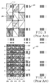
- FIG.1 illustrates a conventional pixel array of a liquid crystal display.
- FIG. 2 illustrates a cross-sectional view of the conventional pixel.
- FIG. 3 illustrates another conventional pixel array of a liquid crystal display.
- FIG. 4 illustrates the conventional pixel array having the "mura" defect when viewing from a certain angle.
- FIG. 5 illustrates a pixel array in accordance with one embodiment of the present invention.
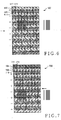
- FIG. 6 illustrates the pixel array when viewing from a first direction in accordance with the embodiment of the present invention.
- FIG. 7 illustrates the pixel array when viewing from a second direction in accordance with the embodiment of the present invention.
- FIG. 8 illustrates another pixel array in accordance with another embodiment of the present invention.
- FIG. 5 illustrates a pixel array 500 in accordance with one embodiment of the present invention.
- the pixel array 500 can be used in various modes of liquid crystal displays, such as the vertically-aligned (VA) mode LCD devices and the twisted-nematic (TN) mode LCD devices.
- VA vertically-aligned
- TN twisted-nematic
- the pixel array 500 is comprised of a plurality of pixels in a rectangular shape where each pixel is divided into two sub-pixels. Each pixel is further divided into a number of domains where the crystal molecules are oriented along different directions.
- the pixel 502 is divided into three portions 508, 510 and 512 by slits 514 and 516, wherein the slit 514 extends from a mid-point of one side of the pixel 502 to a corner of an opposite side of the pixel 502, and the slit 516 extends from the mid-point of one side of the pixel to another corner of the opposite side of the pixel 502.
- the portions 508 and 510 are electrically connected to each other, whereas the portion 512 is electrically disconnected from the other portions 508 and 510.
- the portions 508 and 510 form a first sub-pixel
- the portion 512 forms a second sub-pixel.
- the liquid crystal molecules of the portion 508 are oriented along a direction represented by an arrow 518, and the liquid crystal molecules of the portion 510 are oriented along a direction represented by an arrow 520. Due to the geometry of the slits 514 and 516, the liquid crystal molecules of the upper half of the portion 512 are oriented along a direction represented by an arrow 522, and the liquid crystal molecules of the lower half of the portion 512 are oriented along a direction represented by an arrow 524. The area where the liquid crystal molecules have the same orientation direction is defined as a domain. Thus, the pixel 502 has four domains. These domains improve the viewing angle characteristics for the pixel 502. Further, the pixel 502 has only two slits 514 and 516. Compared to the conventional pixel 102 of FIG.1 that has four protrusions and one slit, the aperture ratio of the pixel 502 is significantly improved.
- the portions 508 and 510 are designed to have a lower threshold voltage, and the portion 512 is designed to have a higher threshold voltage.
- Such arrangement of the high and low threshold voltage portions is repeated for all the pixels in the pixel array 500.
- the shaded areas represent the high threshold portions, and the un-shaded areas represent the low threshold portions.
- the pixels with areas shaded by horizontal lines are charged by a positive polarity, and the pixels with areas shaded by vertical lines are charged by a negative polarity.
- the polarity of the charges may be switched in order to extend the life spans of the pixels. Due to the difference of the polarity, the positively charged pixels and the negatively charged pixels may have slightly different gray levels.
- FIG. 6 illustrates the pixel array of FIG. 5 when viewing from its left side.
- the upper domains 604 and 606 appear to be brighter than the lower domains 608 and 610. Since the domains 604 and 610 are disposed in the first sub-pixel, and the domains 606 and 608 are disposed in the second sub-pixel, which are driven by different voltages, the domain 604 has a lower threshold voltage, it is brighter than the domain 606. Likewise, since the domain 610 has a lower threshold voltage, it is brighter than the domain 608. As such, each pixel has four domains of various gray levels. The un-shaded areas represent the brightest domains.
- the areas shaded with horizontal or vertical lines represent the mid-bright domains.
- the areas shaded with checker patterns represent the darkest domains.
- the areas shaded with slashes represent the mid-dark domains.
- the brightest, mid-bright, mid-dark, and darkest domains are mixed over the whole pixel array 600.
- the pixel array 600 would not have the interwoven bright and dark stripes as shown in FIG. 4.
- the "mura" phenomenon is eliminated.
- FIG. 7 illustrates the pixel array of FIG. 5 when viewing from its right side.
- the upper domains 704 and 706 appear to be darker than the lower domains 708 and 710. Since the domains 704 and 710 are disposed in the first sub-pixel, and the domains 706 and 708 are disposed in the second sub-pixel, which are driven by different voltages, the domain 704 has a lower threshold voltage, it is brighter than the domain 706. Likewise, since the domain 710 has a lower threshold voltage, it is brighter than the domain 708. As such, each pixel has four domains of various gray levels. More specifically, the un-shaded areas represent the brightest domains.
- the areas shaded with horizontal or vertical lines represent the mid-bright domains.
- the areas shaded with checker patterns represent the darkest domains.
- the areas shaded with slashes represent the mid-dark domains.
- the brightest, mid-bright, mid-dark, and darkest domains are mixed over the whole pixel array 700.
- the pixel array 700 would not have the interwoven bright and dark stripes as shown in FIG. 4.
- the "mura" phenomenon is eliminated.
- FIG. 8 illustrates a pixel array 800 in accordance with another embodiment of the present invention.
- the pixel array 800 is comprised of a plurality of pixels in a rectangular shape where each pixel is divided into two sub-pixels. Each pixel is further divided into a number of domains where the crystal molecules are oriented along different directions.
- the pixel 802 is divided into three portions 808, 810 and 812 by silts 14 and 816, wherein the slit 814 extends from a mid-point of one side of the pixel 802 to a corner of an opposite side of the pixel 802, and the slit 816 extends from the mid-point of one side of the pixel to another corner of the opposite side of the pixel 802.
- the portions 808 and 810 are electrically connected to each other, whereas the portion 812 is electrically disconnected from the other portions 808 and 810.
- the portions 808 and 810 form a first sub-pixel
- the portion 812 forms a second sub-pixel.
- the liquid crystal molecules of the portion 808 are oriented along a direction represented by an arrow 818
- the liquid crystal molecules of the portion 810 are oriented along a direction represented by an arrow 820.
- Due to the geometry of the slits 814 and 816 the liquid crystal molecules of the upper half of the portion 812 are oriented along a direction represented by an arrow 822
- the liquid crystal molecules of the lower half of the portion 812 are oriented along a direction represented by an arrow 824.
- the area where the liquid crystal molecules have the same orientation direction is defined as a domain.
- the pixel 802 has four domains. These domains improve the viewing angle characteristics for the pixel 802. Further, the pixel 802 has only two slits 814 and 816. Compared to the conventional pixel 102 of FIG.1 that has four protrusions and one slit, the aperture ratio of the pixel 802 is significantly improved.
- the portions 808 and 810 are designed to have a lower threshold voltage, and the portion 812 is designed to have a higher threshold voltage.
- Such arrangement of the high and low threshold voltage portions is repeated for all the pixels in the pixel array 800.
- the shaded areas represent the high threshold portions, and the un-shaded areas represent the low threshold portions.
- the pixels with areas shaded by horizontal lines are charged by a positive polarity, and the pixels with areas shaded by vertical lines are charged by a negative polarity.
- the polarity of the charges may be switched in order to extend the life spans of the pixels. Due to the difference of polarity, the positively charged pixels and the negatively charged pixels may have slightly different gray levels.
- the pixel array 800 of FIG. 8 differs from the pixel array 500 of FIG. 5 in that the arrangement of the high threshold portions and the low threshold portions are reversed for every two neighboring pixels.
- the pixel array 800 is similar to the pixel array 500 in the sense that when the pixel array 800 is viewed from a certain angle, each pixel will have four domains of various gray levels. As such, the pixel array 800 will not have the interwoven bright and dark stripes as shown in FIG. 4, and therefore, the "mura" phenomenon is eliminated.
- the above embodiments are mere examples for purposes of description. Any alternative of the embodiments capable of eliminating the "mura" defect without reducing the aperture ratio is within the spirit of the invention.
- the slits discussed above can be curves instead of straight lines.
- the locations of the high threshold and low threshold portions can be switched.
Landscapes
- Physics & Mathematics (AREA)
- Nonlinear Science (AREA)
- Mathematical Physics (AREA)
- Chemical & Material Sciences (AREA)
- Crystallography & Structural Chemistry (AREA)
- General Physics & Mathematics (AREA)
- Optics & Photonics (AREA)
- Spectroscopy & Molecular Physics (AREA)
- Geometry (AREA)
- Liquid Crystal (AREA)
Abstract
A liquid crystal display having one or more pixels (502), each of which includes a first sub-pixel (508,510) operating at a first threshold voltage, and a second sub-pixel (512) neighboring the first sub-pixel, and operating at a second threshold voltage. The first sub-pixel is divided into two separate portions (508,510) by the second sub-pixel to form at least four domains of liquid crystal molecules illuminating at various gray levels for improving viewing angle characteristics of the liquid crystal display.
Description
- The present application claims the benefits of
U.S. Provisional Patent Application Serial No. 60/ 782,885 , which was filed on March 15, 2006 and entitled "LIQUID CRYSTAL DISPLAY DEVICE." - The present invention relates to a liquid crystal display, and more particularly to a liquid crystal display with compensated pixel arrays.
- A liquid crystal display is a thin and flat display device comprised of a number of pixels arrayed in front of a light source or reflector. Each pixel contains a layer of liquid crystal molecules between two electrodes. The liquid crystal molecules have electric charges on them. Applying biases to the electrodes creates electrostatic forces that twist the molecules. This twists the light passing through the molecules, and allows varying degrees of light to pass (or not to pass) through the filters. An image can therefore be displayed by those rows and columns of pixels.
- FIG. 1 illustrates a
conventional pixel array 100, in which eachpixel 102 is formed by a first sub-pixel 104 and asecond sub-pixel 106 divided by aslit 120 therebetween. In order to improve viewing angle characteristics, the first andsecond sub-pixels 104 and 106 are designed with different threshold voltages, such that the twosub-pixels 104 and 106 would be charged at different saturation voltage levels when they illuminate. The different saturation voltage levels of the twosub-pixels 104 and 106 cause the liquid crystal molecules therein to have different orientation directions. Thus, this improves the viewing angle characteristics. - In order to further improve the viewing angle characteristics, each sub-pixel 104 is divided into a number of domains, in which the liquid crystal molecules have various orientation directions. For example, the sub-pixel 104 is divided by
protrusions arrow 112, the molecules of the lower-left portion have an orientation direction represented by an arrow 114, and the molecules of the right portion have one orientation direction represented by anarrow 116 for its upper half and another orientation direction represented by anarrow 118 for its lower half. Each portion of an orientation direction defines a domain. Thus, thesub-pixel 102 has four domains. - These various domains improve the viewing angle characteristics. FIG. 2 illustrates a
cross-sectional view 200 of the sub-pixel 104 along line A-A. When theelectrodes protrusion 108 causes the molecules at the right to orient along one direction, and the molecules at the left to orient along another direction. This allows thetop position 206, upper-right position 208, and upperleft position 210 to receive the same amount of light. In other words, the sub-pixel 104 can be viewed from various angles with relatively uniform light transmittance. - One drawback of the
conventional pixel array 100 is that the protrusions and slits reduce its aperture ratio, which refers to the ratio between the area of a pixel that can transmit light and the actual area of the pixel. It is understood by people skilled in the art that more protrusions and slits lead to a lower aperture ratio. As shown in FIG. 1, thesub-pixels 104 and 106 are divided by aslit 120, and each of them includes two protrusions. This reduces the aperture ratio of thepixel 102. - FIG. 3 illustrates another conventional pixel array 300, in which each pixel 302 is formed by a first sub-pixel 304 of a lower threshold voltage and a
second sub-pixel 306 of a higher threshold voltage. As shown in the drawing, eachsub-pixel 304 or 306 only has one protrusion. Thus, the aperture ratio of the pixel 302 is improved. - One drawback of the conventional pixel array 300 is that its pixel arrangement is often susceptible to the "mura" issue, which refers to the non-uniformity of an image over a large area of pixels. Referring to FIGs. 3 and 4 simultaneously, when viewing from the right side of the conventional pixel array 300, certain rows of
sub-pixels 402 would appear to be darker because of their molecule orientations. Thesub-pixel 306 has a higher threshold voltage, so that it appears to be darker when it illuminates. The sub-pixel 304 has a lower threshold voltage, so that it appears to be brighter when it illuminates. As a result,columns 404 would appear to be darker because they are formed by the highthreshold voltage sub-pixels 306, whilecolumns 406 would appear to be brighter because they are formed by low threshold voltage sub-pixels 304. This causes bright and dark stripes interwoven with each other, which is the "mura" defect. - As such, what is needed is a liquid crystal display with a pixel array that provides a high aperture ratio, while being free from the "mura" defect.
- The present invention discloses a liquid crystal display having one or more pixels. In one embodiment of the present invention, each pixel includes a first sub-pixel operating at a first threshold voltage, and a second sub-pixel neighboring the first sub-pixel, and operating at a second threshold voltage. The first sub-pixel is divided into two separate portions by the second sub-pixel to form at least four domains of liquid crystal molecules illuminating at various gray levels for improving viewing angle characteristics of the liquid crystal display.
- The construction and method of operation of the invention, however, together with additional objectives and advantages thereof will be best understood from the following description of specific embodiments when read in connection with the accompanying drawings.
- FIG.1 illustrates a conventional pixel array of a liquid crystal display.
- FIG. 2 illustrates a cross-sectional view of the conventional pixel.
- FIG. 3 illustrates another conventional pixel array of a liquid crystal display.
- FIG. 4 illustrates the conventional pixel array having the "mura" defect when viewing from a certain angle.
- FIG. 5 illustrates a pixel array in accordance with one embodiment of the present invention.
- FIG. 6 illustrates the pixel array when viewing from a first direction in accordance with the embodiment of the present invention.
- FIG. 7 illustrates the pixel array when viewing from a second direction in accordance with the embodiment of the present invention.
- FIG. 8 illustrates another pixel array in accordance with another embodiment of the present invention.
- FIG. 5 illustrates a
pixel array 500 in accordance with one embodiment of the present invention. Thepixel array 500 can be used in various modes of liquid crystal displays, such as the vertically-aligned (VA) mode LCD devices and the twisted-nematic (TN) mode LCD devices. Thepixel array 500 is comprised of a plurality of pixels in a rectangular shape where each pixel is divided into two sub-pixels. Each pixel is further divided into a number of domains where the crystal molecules are oriented along different directions. For example, thepixel 502 is divided into threeportions slits 514 and 516, wherein theslit 514 extends from a mid-point of one side of thepixel 502 to a corner of an opposite side of thepixel 502, and the slit 516 extends from the mid-point of one side of the pixel to another corner of the opposite side of thepixel 502. Theportions 508 and 510 are electrically connected to each other, whereas theportion 512 is electrically disconnected from theother portions 508 and 510. Thus, theportions 508 and 510 form a first sub-pixel, and theportion 512 forms a second sub-pixel. The liquid crystal molecules of theportion 508 are oriented along a direction represented by anarrow 518, and the liquid crystal molecules of the portion 510 are oriented along a direction represented by an arrow 520. Due to the geometry of theslits 514 and 516, the liquid crystal molecules of the upper half of theportion 512 are oriented along a direction represented by an arrow 522, and the liquid crystal molecules of the lower half of theportion 512 are oriented along a direction represented by anarrow 524. The area where the liquid crystal molecules have the same orientation direction is defined as a domain. Thus, thepixel 502 has four domains. These domains improve the viewing angle characteristics for thepixel 502. Further, thepixel 502 has only twoslits 514 and 516. Compared to theconventional pixel 102 of FIG.1 that has four protrusions and one slit, the aperture ratio of thepixel 502 is significantly improved. - The
portions 508 and 510 are designed to have a lower threshold voltage, and theportion 512 is designed to have a higher threshold voltage. Such arrangement of the high and low threshold voltage portions is repeated for all the pixels in thepixel array 500. As shown in FIG. 5, the shaded areas represent the high threshold portions, and the un-shaded areas represent the low threshold portions. The pixels with areas shaded by horizontal lines are charged by a positive polarity, and the pixels with areas shaded by vertical lines are charged by a negative polarity. The polarity of the charges may be switched in order to extend the life spans of the pixels. Due to the difference of the polarity, the positively charged pixels and the negatively charged pixels may have slightly different gray levels. - FIG. 6 illustrates the pixel array of FIG. 5 when viewing from its left side. For each pixel 602, due to the orientations of the liquid crystal molecules, the upper domains 604 and 606 appear to be brighter than the
lower domains domains 604 and 610 are disposed in the first sub-pixel, and thedomains 606 and 608 are disposed in the second sub-pixel, which are driven by different voltages, the domain 604 has a lower threshold voltage, it is brighter than the domain 606. Likewise, since thedomain 610 has a lower threshold voltage, it is brighter than thedomain 608. As such, each pixel has four domains of various gray levels. The un-shaded areas represent the brightest domains. The areas shaded with horizontal or vertical lines represent the mid-bright domains. The areas shaded with checker patterns represent the darkest domains. The areas shaded with slashes represent the mid-dark domains. As shown in FIG. 6, the brightest, mid-bright, mid-dark, and darkest domains are mixed over thewhole pixel array 600. Thus, thepixel array 600 would not have the interwoven bright and dark stripes as shown in FIG. 4. As a result, the "mura" phenomenon is eliminated. - FIG. 7 illustrates the pixel array of FIG. 5 when viewing from its right side. For each
pixel 702, due to the orientations of the liquid crystal molecules, theupper domains 704 and 706 appear to be darker than thelower domains 708 and 710. Since thedomains domain 704 has a lower threshold voltage, it is brighter than the domain 706. Likewise, since thedomain 710 has a lower threshold voltage, it is brighter than the domain 708. As such, each pixel has four domains of various gray levels. More specifically, the un-shaded areas represent the brightest domains. The areas shaded with horizontal or vertical lines represent the mid-bright domains. The areas shaded with checker patterns represent the darkest domains. The areas shaded with slashes represent the mid-dark domains. As shown in FIG. 7, the brightest, mid-bright, mid-dark, and darkest domains are mixed over the whole pixel array 700. Thus, the pixel array 700 would not have the interwoven bright and dark stripes as shown in FIG. 4. As a result, the "mura" phenomenon is eliminated. - FIG. 8 illustrates a
pixel array 800 in accordance with another embodiment of the present invention. Thepixel array 800 is comprised of a plurality of pixels in a rectangular shape where each pixel is divided into two sub-pixels. Each pixel is further divided into a number of domains where the crystal molecules are oriented along different directions. For example, thepixel 802 is divided into threeportions silts 14 and 816, wherein theslit 814 extends from a mid-point of one side of thepixel 802 to a corner of an opposite side of thepixel 802, and theslit 816 extends from the mid-point of one side of the pixel to another corner of the opposite side of thepixel 802. Theportions 808 and 810 are electrically connected to each other, whereas theportion 812 is electrically disconnected from theother portions 808 and 810. Thus, theportions 808 and 810 form a first sub-pixel, and theportion 812 forms a second sub-pixel. The liquid crystal molecules of theportion 808 are oriented along a direction represented by anarrow 818, and the liquid crystal molecules of the portion 810 are oriented along a direction represented by an arrow 820. Due to the geometry of theslits portion 812 are oriented along a direction represented by an arrow 822, and the liquid crystal molecules of the lower half of theportion 812 are oriented along a direction represented by anarrow 824. The area where the liquid crystal molecules have the same orientation direction is defined as a domain. Thus, thepixel 802 has four domains. These domains improve the viewing angle characteristics for thepixel 802. Further, thepixel 802 has only twoslits conventional pixel 102 of FIG.1 that has four protrusions and one slit, the aperture ratio of thepixel 802 is significantly improved. - The
portions 808 and 810 are designed to have a lower threshold voltage, and theportion 812 is designed to have a higher threshold voltage. Such arrangement of the high and low threshold voltage portions is repeated for all the pixels in thepixel array 800. As shown in FIG. 8, the shaded areas represent the high threshold portions, and the un-shaded areas represent the low threshold portions. The pixels with areas shaded by horizontal lines are charged by a positive polarity, and the pixels with areas shaded by vertical lines are charged by a negative polarity. The polarity of the charges may be switched in order to extend the life spans of the pixels. Due to the difference of polarity, the positively charged pixels and the negatively charged pixels may have slightly different gray levels. - The
pixel array 800 of FIG. 8 differs from thepixel array 500 of FIG. 5 in that the arrangement of the high threshold portions and the low threshold portions are reversed for every two neighboring pixels. Thepixel array 800 is similar to thepixel array 500 in the sense that when thepixel array 800 is viewed from a certain angle, each pixel will have four domains of various gray levels. As such, thepixel array 800 will not have the interwoven bright and dark stripes as shown in FIG. 4, and therefore, the "mura" phenomenon is eliminated. - It is noted that the above embodiments are mere examples for purposes of description. Any alternative of the embodiments capable of eliminating the "mura" defect without reducing the aperture ratio is within the spirit of the invention. For example, the slits discussed above can be curves instead of straight lines. As another example, the locations of the high threshold and low threshold portions can be switched.
- The above illustration provides many different embodiments or embodiments for implementing different features of the invention. Specific embodiments of components and processes are described to help clarify the invention. These are, of course, merely embodiments and are not intended to limit the invention from that described in the claims.
- Although the invention is illustrated and described herein as embodied in one or more specific examples, it is nevertheless not intended to be limited to the details shown, since various modifications and structural changes may be made therein without departing from the spirit of the invention and within the scope and range of equivalents of the claims. Accordingly, it is appropriate that the appended claims be construed broadly and in a manner consistent with the scope of the invention, as set forth in the following claims.
Claims (19)
- A liquid crystal display having one or more pixels, each pixel comprising:a first sub-pixel operating at a first threshold voltage; anda second sub-pixel adjacent to the first sub-pixel, and operating at a second threshold voltage,wherein the first sub-pixel is divided into two portions by the second sub-pixel to form at least four domains of liquid crystal molecules illuminating at various gray levels for improving viewing angle characteristics of the liquid crystal display.
- The liquid crystal display of claim 1 wherein the pixel comprises a first slit dividing one portion of the first sub-pixel from the second sub-pixel.
- The liquid crystal display of claim 2 wherein the pixel comprises a second slit dividing the other portion of the first sub-pixel from the second sub-pixel.
- The liquid crystal display of claim 3 wherein the pixel has a rectangular shape.
- The liquid crystal display of claim 4 wherein the first slit extends from a mid-point of one side of the pixel to a corner of an opposite side of the pixel, and the second slit extends from the mid-point of one side of the pixel to another corner of the opposite side of the pixel.
- The liquid crystal display according to any one of claims 1 to 5 wherein the first and second slits are straight lines or curves.
- The liquid crystal display according to any one of claims 1 to 6 wherein the first and second sub-pixels comprise four domains, in which liquid crystal molecules are oriented along four different directions.
- A liquid crystal display having one or more pixels, each pixel comprising:a first sub-pixel operating at a first threshold voltage; anda second sub-pixel neighboring the first sub-pixel, and operating at a second threshold voltage, the first and second sub-pixels being divided to form at least four domains of liquid crystal molecules illuminating at various gray levels for improving viewing angle characteristics of the liquid crystal display,wherein any horizontal cross section of the pixel includes at least one segment of the first sub-pixel and at least one segment of the second sub-pixel, and any vertical cross section of the pixel also includes at least one segment of the first sub-pixel and at least one segment of the second sub-pixel.
- The liquid crystal display of claim 8 wherein the pixel comprises a first slit dividing one portion of the first sub-pixel from the second sub-pixel.
- The liquid crystal display of claim 9 wherein the pixel comprises a second slit dividing another portion of the first sub-pixel from the second sub-pixel.
- The liquid crystal display of claim 10 wherein the pixel has a rectangular shape.
- The liquid crystal display of claim 11 wherein the first slit extends from a mid-point of one side of the pixel to a corner of an opposite side of the pixel, and the second slit extends from the mid-point of one side of the pixel to another corner of the opposite side of the pixel.
- The liquid crystal display according to any one of claims 8 to 12 wherein the first and second sub-pixels comprise four domains, in which liquid crystal molecules are oriented along four different directions.
- A liquid crystal display having a pixel array, which comprises:a first pixel having a first sub-pixel, and a second sub-pixel neighboring the first sub-pixel, wherein the first sub-pixel is divided into first and second portions by the second sub-pixel; anda second pixel adjacent to the first pixel, having a third sub-pixel, and a fourth sub-pixel neighboring the third sub-pixel, wherein the third sub-pixel is divided into third and fourth portions by the fourth sub-pixel,wherein the second and fourth sub-pixels operate at a first threshold voltage and the first and third sub-pixels operate at a second threshold voltage, or the second and third sub-pixels operate at the first threshold voltage and the first and fourth sub-pixels operate at the second threshold voltage.
- The liquid crystal display of claim 14 wherein the first pixel comprises a first slit dividing the first portion of the first sub-pixel from the second sub-pixel, and a second slit dividing the second portion of the first sub-pixel from the second sub-pixel.
- The liquid crystal display of claim 14 wherein the second pixel comprises a third slit dividing the third portion of the third sub-pixel from the fourth sub-pixel, and a fourth slit dividing the fourth portion of the third sub-pixel from the fourth sub-pixel.
- The liquid crystal display according to any one of claims 14 to 16 wherein the first and second pixels are in a rectangular shape.
- The liquid crystal display of claim 17 wherein the first, second, third and fourth sub-pixels are in triangular shapes.
- The liquid crystal display according to any one of claims 14 to 18 wherein the first or second pixel comprise four domains, in which liquid crystal molecules are oriented along four different directions.
Applications Claiming Priority (2)
| Application Number | Priority Date | Filing Date | Title |
|---|---|---|---|
| US78288506P | 2006-03-15 | 2006-03-15 | |
| US11/644,353 US7710524B2 (en) | 2006-03-15 | 2006-12-21 | Liquid crystal display with compensated pixel arrays |
Publications (1)
| Publication Number | Publication Date |
|---|---|
| EP1835332A1 true EP1835332A1 (en) | 2007-09-19 |
Family
ID=37944085
Family Applications (1)
| Application Number | Title | Priority Date | Filing Date |
|---|---|---|---|
| EP07103994A Withdrawn EP1835332A1 (en) | 2006-03-15 | 2007-03-13 | Liquid crystal display with compensated pixel arrays |
Country Status (4)
| Country | Link |
|---|---|
| US (1) | US7710524B2 (en) |
| EP (1) | EP1835332A1 (en) |
| JP (1) | JP4700021B2 (en) |
| TW (1) | TWI353470B (en) |
Families Citing this family (2)
| Publication number | Priority date | Publication date | Assignee | Title |
|---|---|---|---|---|
| JP5348473B2 (en) * | 2009-01-20 | 2013-11-20 | ソニー株式会社 | Liquid crystal display device and electronic device |
| US8786813B2 (en) * | 2010-07-29 | 2014-07-22 | Shenzhen China Star Optoelectronics Technology Co., Ltd. | Liquid crystal display and pixel units thereof |
Citations (2)
| Publication number | Priority date | Publication date | Assignee | Title |
|---|---|---|---|---|
| US20050253797A1 (en) * | 2004-04-30 | 2005-11-17 | Fujitsu Display Technologies Corporation | Liquid crystal display device with improved viewing angle characteristics |
| US20060158576A1 (en) * | 2005-01-14 | 2006-07-20 | Samsung Electronics Co., Ltd. | Thin film transistor panel |
Family Cites Families (10)
| Publication number | Priority date | Publication date | Assignee | Title |
|---|---|---|---|---|
| US5253797A (en) | 1992-07-21 | 1993-10-19 | The United States Of America As Represented By The Secretary Of The Navy | Method of bonding molybdenum to steel |
| JP3966614B2 (en) * | 1997-05-29 | 2007-08-29 | 三星電子株式会社 | Wide viewing angle LCD |
| US6158576A (en) | 1998-10-15 | 2000-12-12 | Albany International Corp. | Endless belt or fabric for use in process control loop |
| KR100898784B1 (en) * | 2002-10-14 | 2009-05-20 | 엘지디스플레이 주식회사 | LCD and its driving method |
| EP1445645A1 (en) * | 2003-02-07 | 2004-08-11 | ZBD Displays Ltd, | Liquid crystal device |
| KR100928487B1 (en) * | 2003-03-28 | 2009-11-26 | 엘지디스플레이 주식회사 | Liquid crystal display |
| JP4464078B2 (en) * | 2003-06-20 | 2010-05-19 | 株式会社 日立ディスプレイズ | Image display device |
| JP4379081B2 (en) | 2003-10-30 | 2009-12-09 | セイコーエプソン株式会社 | Liquid crystal display device and electronic device |
| KR101112539B1 (en) * | 2004-07-27 | 2012-02-15 | 삼성전자주식회사 | Multi-domain liquid crystal display and display panel used therefor |
| JP4460465B2 (en) * | 2005-01-19 | 2010-05-12 | シャープ株式会社 | Liquid crystal display |
-
2006
- 2006-12-21 US US11/644,353 patent/US7710524B2/en active Active
-
2007
- 2007-03-08 TW TW096108001A patent/TWI353470B/en not_active IP Right Cessation
- 2007-03-12 JP JP2007062623A patent/JP4700021B2/en not_active Expired - Fee Related
- 2007-03-13 EP EP07103994A patent/EP1835332A1/en not_active Withdrawn
Patent Citations (2)
| Publication number | Priority date | Publication date | Assignee | Title |
|---|---|---|---|---|
| US20050253797A1 (en) * | 2004-04-30 | 2005-11-17 | Fujitsu Display Technologies Corporation | Liquid crystal display device with improved viewing angle characteristics |
| US20060158576A1 (en) * | 2005-01-14 | 2006-07-20 | Samsung Electronics Co., Ltd. | Thin film transistor panel |
Non-Patent Citations (1)
| Title |
|---|
| SUNATA T ET AL: "A wide-viewing-angle 10-inch-diagonal full-colour active-matrix LCD using a halftone-grayscale method", PROCEEDINGS OF THE INTERNATIONAL DISPLAY RESEARCH CONFERENCE. SAN DIEGO, OCT. 15 - 17, 1991, NEW YORK, IEEE, US, vol. CONF. 11, 15 October 1991 (1991-10-15), pages 255 - 257, XP010053779, ISBN: 0-7803-0213-3 * |
Also Published As
| Publication number | Publication date |
|---|---|
| US20070216844A1 (en) | 2007-09-20 |
| JP4700021B2 (en) | 2011-06-15 |
| US7710524B2 (en) | 2010-05-04 |
| JP2007249203A (en) | 2007-09-27 |
| TW200734742A (en) | 2007-09-16 |
| TWI353470B (en) | 2011-12-01 |
Similar Documents
| Publication | Publication Date | Title |
|---|---|---|
| CN100495136C (en) | Liquid crystal display device and method of driving the same | |
| US6958791B2 (en) | Liquid crystal display | |
| US7429981B2 (en) | Liquid crystal display | |
| EP2669882B1 (en) | Display device and driving method thereof | |
| JP5193511B2 (en) | Liquid crystal display panel, driving method thereof, and liquid crystal display device | |
| US20110050683A1 (en) | Three-dimensional display device | |
| KR101366459B1 (en) | Liquid crystal display device | |
| US8212950B2 (en) | Liquid crystal display panel and liquid crystal display | |
| CN103257480A (en) | Alignment method for liquid crystal VA model | |
| US7876410B2 (en) | Multi-domain vertically aligned liquid crystal display having a plurality of jagged and non-jagged slits | |
| US10788721B2 (en) | Liquid crystal display | |
| CN100523929C (en) | Liquid crystal display device with a light guide plate | |
| EP1873748A3 (en) | Triangular arrangement of subpixels on both sides of a common data line in an active matrix LCD | |
| JP5589018B2 (en) | Liquid crystal display | |
| US7710524B2 (en) | Liquid crystal display with compensated pixel arrays | |
| CN102483545A (en) | Liquid crystal display | |
| CN115343871B (en) | Display panel and display device | |
| CN111258130A (en) | Liquid crystal display panel | |
| CN209911724U (en) | Pixel electrode, pixel assembly and display panel | |
| GB2425641A (en) | Multi-domain vertical alignment liquid crystal display with slits to pixel electrode |
Legal Events
| Date | Code | Title | Description |
|---|---|---|---|
| PUAI | Public reference made under article 153(3) epc to a published international application that has entered the european phase |
Free format text: ORIGINAL CODE: 0009012 |
|
| AK | Designated contracting states |
Kind code of ref document: A1 Designated state(s): AT BE BG CH CY CZ DE DK EE ES FI FR GB GR HU IE IS IT LI LT LU LV MC MT NL PL PT RO SE SI SK TR |
|
| AX | Request for extension of the european patent |
Extension state: AL BA HR MK YU |
|
| AKX | Designation fees paid | ||
| STAA | Information on the status of an ep patent application or granted ep patent |
Free format text: STATUS: THE APPLICATION IS DEEMED TO BE WITHDRAWN |
|
| 18D | Application deemed to be withdrawn |
Effective date: 20080320 |
|
| REG | Reference to a national code |
Ref country code: DE Ref legal event code: 8566 |