EP1835312A2 - Illumination device for a microlithographic projection apparatus having an element made of uniaxial crystal and having a plurality of refractive or diffractive structures extending along an axis being parallel or perpendicular to the crystal axis - Google Patents
Illumination device for a microlithographic projection apparatus having an element made of uniaxial crystal and having a plurality of refractive or diffractive structures extending along an axis being parallel or perpendicular to the crystal axis Download PDFInfo
- Publication number
- EP1835312A2 EP1835312A2 EP07103867A EP07103867A EP1835312A2 EP 1835312 A2 EP1835312 A2 EP 1835312A2 EP 07103867 A EP07103867 A EP 07103867A EP 07103867 A EP07103867 A EP 07103867A EP 1835312 A2 EP1835312 A2 EP 1835312A2
- Authority
- EP
- European Patent Office
- Prior art keywords
- optical system
- light
- conductance
- anyone
- crystal material
- Prior art date
- Legal status (The legal status is an assumption and is not a legal conclusion. Google has not performed a legal analysis and makes no representation as to the accuracy of the status listed.)
- Granted
Links
Images




Classifications
-
- G—PHYSICS
- G03—PHOTOGRAPHY; CINEMATOGRAPHY; ANALOGOUS TECHNIQUES USING WAVES OTHER THAN OPTICAL WAVES; ELECTROGRAPHY; HOLOGRAPHY
- G03F—PHOTOMECHANICAL PRODUCTION OF TEXTURED OR PATTERNED SURFACES, e.g. FOR PRINTING, FOR PROCESSING OF SEMICONDUCTOR DEVICES; MATERIALS THEREFOR; ORIGINALS THEREFOR; APPARATUS SPECIALLY ADAPTED THEREFOR
- G03F7/00—Photomechanical, e.g. photolithographic, production of textured or patterned surfaces, e.g. printing surfaces; Materials therefor, e.g. comprising photoresists; Apparatus specially adapted therefor
- G03F7/70—Microphotolithographic exposure; Apparatus therefor
- G03F7/70058—Mask illumination systems
- G03F7/70075—Homogenization of illumination intensity in the mask plane by using an integrator, e.g. fly's eye lens, facet mirror or glass rod, by using a diffusing optical element or by beam deflection
-
- G—PHYSICS
- G02—OPTICS
- G02B—OPTICAL ELEMENTS, SYSTEMS OR APPARATUS
- G02B1/00—Optical elements characterised by the material of which they are made; Optical coatings for optical elements
- G02B1/02—Optical elements characterised by the material of which they are made; Optical coatings for optical elements made of crystals, e.g. rock-salt, semi-conductors
-
- G—PHYSICS
- G02—OPTICS
- G02B—OPTICAL ELEMENTS, SYSTEMS OR APPARATUS
- G02B1/00—Optical elements characterised by the material of which they are made; Optical coatings for optical elements
- G02B1/08—Optical elements characterised by the material of which they are made; Optical coatings for optical elements made of polarising materials
-
- G—PHYSICS
- G02—OPTICS
- G02B—OPTICAL ELEMENTS, SYSTEMS OR APPARATUS
- G02B3/00—Simple or compound lenses
- G02B3/0006—Arrays
- G02B3/0037—Arrays characterized by the distribution or form of lenses
- G02B3/005—Arrays characterized by the distribution or form of lenses arranged along a single direction only, e.g. lenticular sheets
-
- G—PHYSICS
- G02—OPTICS
- G02B—OPTICAL ELEMENTS, SYSTEMS OR APPARATUS
- G02B3/00—Simple or compound lenses
- G02B3/0006—Arrays
- G02B3/0037—Arrays characterized by the distribution or form of lenses
- G02B3/0062—Stacked lens arrays, i.e. refractive surfaces arranged in at least two planes, without structurally separate optical elements in-between
- G02B3/0068—Stacked lens arrays, i.e. refractive surfaces arranged in at least two planes, without structurally separate optical elements in-between arranged in a single integral body or plate, e.g. laminates or hybrid structures with other optical elements
-
- G—PHYSICS
- G02—OPTICS
- G02B—OPTICAL ELEMENTS, SYSTEMS OR APPARATUS
- G02B5/00—Optical elements other than lenses
- G02B5/18—Diffraction gratings
- G02B5/1814—Diffraction gratings structurally combined with one or more further optical elements, e.g. lenses, mirrors, prisms or other diffraction gratings
- G02B5/1819—Plural gratings positioned on the same surface, e.g. array of gratings
- G02B5/1823—Plural gratings positioned on the same surface, e.g. array of gratings in an overlapping or superposed manner
-
- G—PHYSICS
- G02—OPTICS
- G02B—OPTICAL ELEMENTS, SYSTEMS OR APPARATUS
- G02B5/00—Optical elements other than lenses
- G02B5/18—Diffraction gratings
- G02B5/1833—Diffraction gratings comprising birefringent materials
-
- G—PHYSICS
- G02—OPTICS
- G02B—OPTICAL ELEMENTS, SYSTEMS OR APPARATUS
- G02B5/00—Optical elements other than lenses
- G02B5/18—Diffraction gratings
- G02B5/1838—Diffraction gratings for use with ultraviolet radiation or X-rays
-
- G—PHYSICS
- G02—OPTICS
- G02B—OPTICAL ELEMENTS, SYSTEMS OR APPARATUS
- G02B5/00—Optical elements other than lenses
- G02B5/18—Diffraction gratings
- G02B5/1866—Transmission gratings characterised by their structure, e.g. step profile, contours of substrate or grooves, pitch variations, materials
-
- G—PHYSICS
- G03—PHOTOGRAPHY; CINEMATOGRAPHY; ANALOGOUS TECHNIQUES USING WAVES OTHER THAN OPTICAL WAVES; ELECTROGRAPHY; HOLOGRAPHY
- G03B—APPARATUS OR ARRANGEMENTS FOR TAKING PHOTOGRAPHS OR FOR PROJECTING OR VIEWING THEM; APPARATUS OR ARRANGEMENTS EMPLOYING ANALOGOUS TECHNIQUES USING WAVES OTHER THAN OPTICAL WAVES; ACCESSORIES THEREFOR
- G03B27/00—Photographic printing apparatus
- G03B27/72—Controlling or varying light intensity, spectral composition, or exposure time in photographic printing apparatus
-
- G—PHYSICS
- G03—PHOTOGRAPHY; CINEMATOGRAPHY; ANALOGOUS TECHNIQUES USING WAVES OTHER THAN OPTICAL WAVES; ELECTROGRAPHY; HOLOGRAPHY
- G03F—PHOTOMECHANICAL PRODUCTION OF TEXTURED OR PATTERNED SURFACES, e.g. FOR PRINTING, FOR PROCESSING OF SEMICONDUCTOR DEVICES; MATERIALS THEREFOR; ORIGINALS THEREFOR; APPARATUS SPECIALLY ADAPTED THEREFOR
- G03F7/00—Photomechanical, e.g. photolithographic, production of textured or patterned surfaces, e.g. printing surfaces; Materials therefor, e.g. comprising photoresists; Apparatus specially adapted therefor
- G03F7/70—Microphotolithographic exposure; Apparatus therefor
- G03F7/70058—Mask illumination systems
- G03F7/7015—Details of optical elements
- G03F7/70158—Diffractive optical elements
-
- G—PHYSICS
- G03—PHOTOGRAPHY; CINEMATOGRAPHY; ANALOGOUS TECHNIQUES USING WAVES OTHER THAN OPTICAL WAVES; ELECTROGRAPHY; HOLOGRAPHY
- G03F—PHOTOMECHANICAL PRODUCTION OF TEXTURED OR PATTERNED SURFACES, e.g. FOR PRINTING, FOR PROCESSING OF SEMICONDUCTOR DEVICES; MATERIALS THEREFOR; ORIGINALS THEREFOR; APPARATUS SPECIALLY ADAPTED THEREFOR
- G03F7/00—Photomechanical, e.g. photolithographic, production of textured or patterned surfaces, e.g. printing surfaces; Materials therefor, e.g. comprising photoresists; Apparatus specially adapted therefor
- G03F7/70—Microphotolithographic exposure; Apparatus therefor
- G03F7/70483—Information management; Active and passive control; Testing; Wafer monitoring, e.g. pattern monitoring
- G03F7/7055—Exposure light control in all parts of the microlithographic apparatus, e.g. pulse length control or light interruption
- G03F7/70566—Polarisation control
-
- G—PHYSICS
- G03—PHOTOGRAPHY; CINEMATOGRAPHY; ANALOGOUS TECHNIQUES USING WAVES OTHER THAN OPTICAL WAVES; ELECTROGRAPHY; HOLOGRAPHY
- G03F—PHOTOMECHANICAL PRODUCTION OF TEXTURED OR PATTERNED SURFACES, e.g. FOR PRINTING, FOR PROCESSING OF SEMICONDUCTOR DEVICES; MATERIALS THEREFOR; ORIGINALS THEREFOR; APPARATUS SPECIALLY ADAPTED THEREFOR
- G03F7/00—Photomechanical, e.g. photolithographic, production of textured or patterned surfaces, e.g. printing surfaces; Materials therefor, e.g. comprising photoresists; Apparatus specially adapted therefor
- G03F7/70—Microphotolithographic exposure; Apparatus therefor
- G03F7/708—Construction of apparatus, e.g. environment aspects, hygiene aspects or materials
- G03F7/7095—Materials, e.g. materials for housing, stage or other support having particular properties, e.g. weight, strength, conductivity, thermal expansion coefficient
- G03F7/70958—Optical materials or coatings, e.g. with particular transmittance, reflectance or anti-reflection properties
-
- G—PHYSICS
- G03—PHOTOGRAPHY; CINEMATOGRAPHY; ANALOGOUS TECHNIQUES USING WAVES OTHER THAN OPTICAL WAVES; ELECTROGRAPHY; HOLOGRAPHY
- G03F—PHOTOMECHANICAL PRODUCTION OF TEXTURED OR PATTERNED SURFACES, e.g. FOR PRINTING, FOR PROCESSING OF SEMICONDUCTOR DEVICES; MATERIALS THEREFOR; ORIGINALS THEREFOR; APPARATUS SPECIALLY ADAPTED THEREFOR
- G03F7/00—Photomechanical, e.g. photolithographic, production of textured or patterned surfaces, e.g. printing surfaces; Materials therefor, e.g. comprising photoresists; Apparatus specially adapted therefor
- G03F7/70—Microphotolithographic exposure; Apparatus therefor
- G03F7/708—Construction of apparatus, e.g. environment aspects, hygiene aspects or materials
- G03F7/7095—Materials, e.g. materials for housing, stage or other support having particular properties, e.g. weight, strength, conductivity, thermal expansion coefficient
- G03F7/70958—Optical materials or coatings, e.g. with particular transmittance, reflectance or anti-reflection properties
- G03F7/70966—Birefringence
Definitions
- the invention relates to an optical system of an illumination device of a microlithographic projection exposure apparatus, comprising at least one light-conductance-increasing element, in which a generation of light conductance is made possible whilst maintaining the polarization state.
- DOEs diffractive optical elements
- a desired intensity distribution e.g. dipole or quadrupole distribution
- an angular emission characteristic of the DOE that is defined by the respective diffracting surface structure, e.g. in a pupil plane.
- the material of the DOE When used in ranges of high energy density of the laser beam, the material of the DOE is subjected to very great loading.
- the short-wave laser light leads to so-called compacting, i.e. local density changes and local anisotropies in the material.
- a further nondeterministic birefringence distribution is finally established also owing to absorption and the associated heat input and the resultant strains of the material, and destroys the polarization state of the laser light, which can then only be avoided by exchanging the DOE.
- a destruction of the polarization state of the laser light can also result when the DOE is formed from isotropic crystal material, owing to crystal structural defects, stress-induced and/or intrinsic birefringence.
- An optical system has at least one first light-conductance-increasing element having a plurality of diffractively or refractively beam-deflecting structures extending in a common first preferred direction, the light-conductance-increasing element having an optically uniaxial crystal material in such a way that the optical crystal axis of said crystal material is substantially parallel or substantially perpendicular to the first preferred direction.
- the "light conductance” is also referred to "etendue”.
- the birefringent material is preferably used such that it is irradiated with characteristic states with regard to the polarization, and the deflecting (diffractive or refractive) structures are arranged parallel or perpendicular to the characteristic states. What is thereby achieved is that the induced birefringence effects play no or only a secondary part with regard to polarization.
- the beam-deflecting structures are formed on a substrate composed of optically uniaxial crystal material, the optical crystal axis of said crystal material being oriented substantially parallel to the substrate surface.
- the plurality of beam-deflecting structures of the first light-conductance-increasing element is formed by an arrangement of cylindrical lenses. According to a further embodiment, the plurality of beam-deflecting structures of the first light-conductance-increasing element can be formed by a diffractive optical element (DOE).
- DOE diffractive optical element
- the diffractive optical element can be a Computer Generated Hologram (CGH).
- This Computer Generated Hologram can comprise an array of facet areas. Each of said facet areas can comprise a structure which may be calculated by computer in order to achieve the desired beam-deflecting effect, or angular-spread, respectively.
- the Computer Generated Hologram also comprises a substrate being made of a birefringent, optically uniaxial material.
- the diffractive optical element in particular a Computer Generated Hologram (CGH) may generate a desired two-dimensional intensity distribution (which may in particular have a n-fold symmetry, as given for example in dipole or quadrupole distribution) by way of an angle radiation characteristic defined by the respective beam-deflecting structure.
- DOE Computer Generated Hologram
- this preferred direction can be defined, in the case of a Computer Generated Hologram (CGH), as the direction being oriented from the optical system axis of the illumination device towards an extremum of said two-dimensional intensity distribution.
- the preferred direction may also be defined, if applied to a Computer Generated Hologram (CGH), not on the basis of the specific surface structure of the CGH, but on the basis of the beam deflecting effect which is achieved due to this surface structure.
- CGH Computer Generated Hologram
- the optical crystal axis of said crystal material of the substrate is either substantially parallel or substantially perpendicular to said preferred direction.
- said array of facet areas can be formed such that said structures of said Computer Generated Hologram (CGH) comprise no discontinuity across a border between adjacent facet areas, as disclosed e.g. in US 5,850,300 and with the advantages described therein.
- the structures provided in the individual facet areas of the Computer Generated Hologram (CGH) behave substantially continuous across borders between adjacent facet areas.
- discontinuities e.g. edges, breaks or the like
- a continuous transition of the phase function can be provided at the borders between the adjacent facet areas, thereby eliminating intensity variations to occur at such borders.
- said array of facet areas can be formed such that said structures of said Computer Generated Hologram (CGH) comprise a discontinuity across a border between adjacent facet areas, which may e.g. be useful in providing a greater freedom of design.
- CGH Computer Generated Hologram
- said array of facet areas is formed such that said structures of said Computer Generated Hologram (CGH) are replicated in no one of said facet areas, which may be useful in order to avoid repeated undesired intensity variations by interaction of structures belonging to different facet areas.
- CGH Computer Generated Hologram
- said array of facet areas can be formed such that said structures of said Computer Generated Hologram (CGH) are replicated in at least one facet area of said facet areas.
- CGH Computer Generated Hologram
- said facet areas have a polygonal shape and are arranged pairwise adjacent to each other.
- This polygonal shape can particularly be selected from the group consisting of triangle, rectangle, square and hexagon.
- facet areas being adjacent to each other have different cross-sections, which may be useful in order to avoid repeated undesired intensity variations by interaction of structures belonging to different facet areas.
- facet areas being adjacent to each other are alike with regard to their cross-section.
- the diffractive optical element (DOE) is formed in such a way that the blaze effect is greater for one of two mutually perpendicular polarization states than for the other of said polarization states.
- said two mutually perpendicular polarization states are s-polarization and p-polarization.
- the s-polarized component of light impinging on the diffractive optical element (DOE) is predominantly directed into the ⁇ 1st order of diffraction and the p-polarized component of light impinging on the diffractive optical element (DOE) is predominantly directed into the zeroth order of diffraction.
- the optically uniaxial crystal material is a non-optically-active material.
- the optically uniaxial crystal material is an optically active material which is present both in a levorotatory and in a dextrorotatory form.
- the optically uniaxial crystal material has a fluoride compound.
- the optically uniaxial crystal material has a nitride compound.
- the optically uniaxial crystal material has an oxide compound.
- the optically uniaxial crystal material may be selected, in particular, from the group containing crystalline quartz (SiO 2 ), magnesium fluoride (MgF 2 ), lanthanum fluoride (LaF 3 ) and sapphire (Al 2 O 3 ).
- a second light-conductance-increasing element is disposed downstream of the first light-conductance-increasing element in the light propagation direction, and has a plurality of diffractively or refractively beam-deflecting structures extending in a second preferred direction, the second preferred direction being different from the first preferred direction.
- the second preferred direction is substantially perpendicular to the first preferred direction.
- the second light-conductance-increasing element is produced from an optically isotropic material at least in the region of the beam-deflecting structures.
- the beam-deflecting structures e.g. cylindrical lenses
- the beam-deflecting structures may be produced from an optically isotropic material.
- the isotropic material may be selected, in particular, from the group containing calcium fluoride (CaF 2 ), strontium fluoride (SrF 2 ), magnesium oxide (MgO) and YAG.
- the isotropic material may furthermore also be an amorphous material, in particular quartz glass.
- the beam-deflecting structures of the second light-conductance-increasing element are formed on a substrate composed of optically uniaxial crystal material.
- the optical crystal axis of said crystal material is preferably oriented substantially parallel to the substrate surface.
- the optical crystal axis of the crystal material of the second light-conductance-increasing element is substantially parallel or substantially perpendicular to the second preferred direction.
- the plurality of beam-deflecting structures of the second light-conductance-increasing element may be formed both by an arrangement of cylindrical lenses and by a diffractive optical element.
- a first light mixing device is arranged between the first light-conductance-increasing element and the second light-conductance-increasing element.
- the first light mixing device is an integrator rod.
- the first light-conductance-increasing element can be arranged at a light entrance surface of the integrator rod.
- At least one second light mixing device is arranged on that side of the second light-conductance-increasing element which is remote from the first light-conductance-increasing element.
- the second light mixing device is an integrator rod.
- the second light mixing device comprises a plurality of integrator rods which are arranged successively in the light propagation direction and between which a light-conductance-increasing element is in each case arranged.
- At least one integrator rod of the first integrator rod, the second integrator rod and the further integrator rods is produced from a birefringent material, in particular quartz (SiO 2 ), magnesium fluoride (MgF 2 ), lanthanum fluoride (LaF 3 ) or sapphire (Al 2 O 3 ).
- a birefringent material in particular quartz (SiO 2 ), magnesium fluoride (MgF 2 ), lanthanum fluoride (LaF 3 ) or sapphire (Al 2 O 3 ).
- the invention also relates to a diffractive optical element comprising at least one first blaze grating and a second blaze grating, the second blaze grating being superimposed on a light exit surface of the first blaze grating and having a substantially ribbed arrangement of substructures which are smaller than an operating wavelength for which the diffractive optical element (DOE) is designed, characterized in that the diffractive optical element has an optically uniaxial crystal material, the optical crystal axis of said crystal material being substantially parallel or substantially perpendicular to grating structures of the first and/or the second blaze grating.
- DOE diffractive optical element
- the optically uniaxial crystal material has a fluoride compound.
- the optically uniaxial crystal material has a nitride compound.
- the optically uniaxial crystal material has a non-semiconducting oxide compound.
- the optically uniaxial crystal material has a refractive index n of at least 1.6 at an operating wavelength for which the optical system is designed.
- the invention also relates to a diffractive optical element, a microlithographic projection exposure apparatus, a method for the microlithographic production of microstructured components, and a microstructured component.
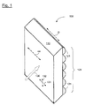
- Fig. 1 shows a light-conductance-increasing element 100 in accordance with a first embodiment of the present invention.
- the element 100 in accordance with Fig. 1 is formed from a carrier plate 110 composed of optically uniaxial, birefringent crystal material, which is magnesium fluoride (MgF 2 ) in accordance with the exemplary embodiment.
- a carrier plate 110 composed of optically uniaxial, birefringent crystal material, which is magnesium fluoride (MgF 2 ) in accordance with the exemplary embodiment.
- a plurality of beam-deflecting structures 120 which, in accordance with the exemplary embodiment, is formed by an arrangement of cylindrical lenses 121, in such a way that the direction (designated by "D” in Fig. 1) of the longitudinal axes of said cylindrical lenses 121 is parallel to one another and also parallel to the optical crystal axis - designated by "oa" - of the optically uniaxial crystal material of the carrier plate 110.
- the cylindrical lenses 121 of the element 100 are likewise produced on an optically uniaxial crystal material, namely composed of magnesium fluoride (MgF 2 ) in accordance with the exemplary embodiment.
- MgF 2 magnesium fluoride
- the optical activity must be taken into consideration when using crystalline quartz. If the crystal axis is oriented in the plate or substrate plane and illumination is effected in a collimated manner perpendicular to the plate or substrate plane, there is no effect. In all other cases, the harmful effect can also be prevented by combination of levorotatory and dextrorotatory quartz.
- the carrier plate 110 and the cylindrical lenses 121 may comprise the same crystal material or else different crystal materials. Furthermore, the cylindrical lenses 121 may also have a planoconcave form instead of the planoconvex form shown in Fig. 1, and may furthermore also be arranged alternatively at the light entrance surface of the carrier plate 110.
- the element 100 in accordance with Fig. 1 serves for use in an optical system, in particular in an illumination device of a microlithographic projection exposure apparatus (not illustrated in Fig. 1), a light propagation direction of the light impinging on the element 100 being indicated on the basis of the arrow 130 in Fig. 1.
- the arrow 131 is used to designate the preferred direction of polarization of said light, i.e. in the case of linearly polarized light the direction of vibration of the electric field vector E.
- said preferred direction of polarization runs parallel to the optical crystal axis "oa".
- the direction of polarization may also be oriented perpendicular to the optical crystal axis "oa".
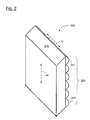
- a light-conductance-increasing optical element 200 illustrated in Fig. 2 corresponds to the element 100 illustrated in Fig. 1, corresponding elements having been designed by reference numerals increased by 100.
- the element 200 differs from the element 100 only by virtue of the fact that the optical crystal axis "oa" of the material of the carrier plate 210 runs perpendicular to the direction - designated by "D" - of the longitudinal axes of the cylindrical lenses 221.
- an optical system 300 in accordance with a further preferred embodiment of the invention comprises, in addition to a first light-conductance-increasing element 300a (the construction of which in the exemplary embodiment corresponds to that from Fig. 1), a second light-conductance-increasing element 300b.
- the first element 300a has, at the light exit surface of a carrier plate 310, a plurality of cylindrical lenses 321 whose longitudinal axis (designed by "D1" in Fig. 3), as in Fig. 1, is parallel to the optical crystal axis "oa-1" of the crystal material of the carrier plate 310.
- the second light-conductance-increasing element 300b comprises a carrier plate 330 composed of optically uniaxial crystalline material (for example MgF 2 ) whose optical crystal axis "oa-2" is parallel to the optical crystal axis "oa-1" of the crystal material of the first carrier plate 310.
- a carrier plate 330 composed of optically uniaxial crystalline material (for example MgF 2 ) whose optical crystal axis "oa-2" is parallel to the optical crystal axis "oa-1" of the crystal material of the first carrier plate 310.
- an arrangement 340 of cylindrical lenses 341 Situated at the light exit surface of the carrier plate 330 of the second element 300b is an arrangement 340 of cylindrical lenses 341, the orientation (designated by "D2" in Fig. 3) of the longitudinal axes of said cylindrical lenses 341 being perpendicular to the orientation "D1" of the cylindrical lenses 321.
- the optical system 300 comprises, in particular, mutually crossed arrangements 320 and 340 of cylindrical lenses 321 and 341, respectively, by means of which, as likewise indicated in Fig. 3, light conductance is increased in two mutually perpendicular spatial directions (in the x-direction and in the y-direction in accordance with the system of coordinates indicated in the figure).
- the cylindrical lenses 341 of the arrangement 340 do not comprise optically uniaxial crystal material, but rather are composed of optically isotropic material, in particular cubically crystalline material.
- said optically isotropic material is calcium fluoride (CaF 2 ), but it is also possible to use another material transparent at the operating wavelength, for example strontium fluoride (SrF 2 ), magnesium oxide (MgO) or YAG.
- an amorphous material, in particular quartz glass may also be used as the optically isotropic material.
- the arrangements 320 and 340 of the cylindrical lenses 321 and 341, respectively, may alternatively also be provided at the light entrance surface of the respective carrier plate 310 and 330.
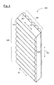
- crossed cylindrical lens arrangements 420 and 430 having cylindrical lenses 421 and 431, respectively, may also be formed on a common carrier plate 410.
- the material of the carrier plate 410 is once again an optically uniaxial crystal material (for example MgF 2 ), the optical crystal axis "oa" in the exemplary embodiment being parallel to the orientation "D1" of the longitudinal axes of the cylindrical lenses 421 and perpendicular to the orientation "D2" of the longitudinal axes of the cylindrical lenses 431.
- the cylindrical lenses 421 of the first arrangement 420 are produced from optically uniaxial crystal material
- the cylindrical lenses 431 forming the second arrangement 430 are produced from optically isotropic material.
- a first light-conductance-increasing element 500a is arranged at the light entrance surface of an integrator rod 520
- a second light-conductance-increasing element 500b is arranged at the light exit surface of the integrator rod 520.
- the construction of the first and second light-conductance-increasing elements 500a and 500b, respectively, corresponds to that of the first and second light-conductance-increasing elements 300a and 300b, respectively, from Fig. 3, and so a detailed description is dispensed with here.
- the integrator rod 520 is in turn produced from an optically uniaxial crystal material, for example MgF 2 .
- the first light-conductance-increasing element 500a brings about an increase in the light conductance in a first spatial direction, namely in the positive and negative y-direction in accordance with the system of coordinates indicated.
- the integrator rod 520 By means of the integrator rod 520, light mixing is likewise effected in the y-direction, with the result that only two of the lateral surfaces of the integrator rod 520 (the upper and lower surfaces in Fig. 5) have to be machined in optically plane-parallel fashion.
- the second light-conductance-increasing element 500b brings about an increase in the light conductance and also intermixing of the light emerging from the integrator rod 520 in a second spatial direction (in the positive and negative x-direction in accordance with Fig. 5) perpendicular to the first spatial direction.
- further light-conductance-increasing elements may be disposed downstream of the light-conductance-increasing element 500b shown in Fig. 5, which further light-conductance-increasing elements bring about a further intermixing of the light emerging from the second element 500b.
- a first light-conductance-increasing element 610 is arranged at the light entrance surface of a first integrator rod 620, and a second light-conductance-increasing element 630 is arranged at the light exit surface of the integrator rod 620.
- the first light-conductance-increasing element 610 results in an expansion perpendicular to the plane of the drawing (in the positive and negative x-direction in accordance with the system of coordinates indicated in the figure), and the second light-conductance-increasing element 630 results in aperture generation in the plane of the drawing (i.e. in the positive and negative y-direction).
- a third light-conductance-increasing element 640, a second integrator rod 650, a fourth light-conductance-increasing element 670 and a third integrator rod 660 are arranged successively downstream of the second light-conductance-increasing element 630 in the light propagation direction (x-direction).
- the light mixing device disposed downstream of the second light-conductance-increasing element 620 comprises a plurality of integrator rods 650, 660 ... which are arranged successively in the light propagation direction and between which a further light-conductance-increasing element 670, ... is in each case arranged.
- a further light-conductance-increasing element 670, ... is in each case arranged.
- the integrator rod 620 is once again preferably produced from an optically uniaxial crystal material, e.g. MgF 2 , the optical crystal axis "oa", analogously to the embodiment of Fig. 5, once again being parallel to the preferred direction of the beam-deflecting structures of the first light-conductance-increasing element 610 and perpendicular to the preferred direction of the beam-deflecting structures of the second light-conductance-increasing element 630 (or visa versa).
- the light-conductance-increasing element 610, 630, 640 and 670 in accordance with Fig. 6 are formed as diffractive optical elements (DOEs), so that the respective preferred direction of the beam-deflecting structures in each case corresponds to the extending direction of the linear structures present on said DOEs.
- DOEs diffractive optical elements
- the integrator rods 650 and 660 are formed from optically isotropic material, MgAl 2 O 4 in the exemplary embodiment.
- optically isotropic material MgAl 2 O 4 in the exemplary embodiment.
- another cubically crystalline material or else an amorphous material e.g. quartz glass
- the optical system 600 shown in Fig. 6 is preferably arranged upstream of the input of a REMA objective present in an illumination device of a microlithographic projection apparatus.
- DOEs may also be arranged, and vice versa.
- a corresponding arrangement 710 comprising a first DOE 712 arranged on a first carrier 711 and a second DOE 714 arranged on a second carrier 713, said second DOE being disposed downstream in the light propagation direction, the DOEs 712 and 714 in each case bringing about light conductance increases in mutually perpendicular spatial directions.
- the DOE may be formed in a known manner by the formation of light-opaque structures on a carrier or in the form of light-transmissive structures in specific regions with a varying refractive index and/or varying geometrical thickness. These structures of a DOE may be performed for example by corresponding material removal in a carrier plate composed of optically uniaxial crystal material.
- an amorphous layer composed of quartz glass may also be vapor-deposited onto a carrier plate composed of optically uniaxial crystal material, into which layer the patterning is subsequently introduced by etching.
- the latter embodiment has the advantage that a more uniform formation of the edges present in the structures is possible in the case of patterning of the amorphous layer than in the case of direct patterning of the crystalline carrier plate.
- the carrier 711 (and thus, in the case of integral formation with the DOE, also the structures of the DOE 712) is produced from optically uniaxial crystal material, e.g. MgF 2 .
- the carrier 713 is preferably produced, analogously to the embodiment of Fig. 3, from an optically isotropic material, i.e. either a cubically crystalline material or an amorphous material (e.g. quartz glass).
- the second carrier 713 is produced from optically uniaxial crystal material in the same way as the first carrier, and the DOE 714 is produced by vapor deposition and subsequent etching of an amorphous layer, in particular composed of quartz glass.
- DOEs 712, 714 may also be arranged on the respective light entrance surface of the carrier 711 and 713.
- DOEs 722 and 723 also to be arranged on a common carrier 721.
- the carrier 721 is produced from an optically uniaxial crystal material, e.g. MgF 2 , and the DOE 723 arranged at the light exit surface of the carrier 721 is formed, as described above, by vapor deposition and etching of an amorphous layer composed of e.g. quartz glass.
- the DOE 722 arranged at the light entrance surface of the carrier 721 may optionally be formed from optically uniaxial crystal material (that is say in particular integrally with the carrier 721 by means of corresponding material removal) or likewise by means of vapor deposition and etching of an amorphous layer composed of e.g. quartz glass.
- a more complex DOE structure 732 with deflection in arbitrary spatial directions on a carrier 731 (once again composed of optically uniaxial crystal material), which structure is once again produced by vapor deposition and etching of an amorphous layer composed of e.g. quartz glass.
- the diffractive optical elements (DOEs) used according to the invention which have an optically uniaxial crystal material as explained above may also be equipped with a blaze effect in order to direct radiation intensity into a desired order of diffraction, in particular for instance the first order of diffraction, in a targeted manner.
- the respective DOE may be formed with a typically sawtooth or stepped profile with corresponding periodic structures 801, 802, 803, ..., as shown in an exemplary schematic arrangement 800 with reference to Fig. 8a.
- a DOE according to the invention which has an optically uniaxial crystal material as explained above is formed in polarization-selective fashion in such a way that the blaze effect is greater for one of two mutually perpendicular polarization states (in particular s-polarization and p-polarization) than for the other of said polarization states.
- the DOE may be formed in such a way that the s-polarized component of light impinging on the DOE is predominantly directed into the ⁇ 1st order of diffraction and the p-polarized component of light impinging on the DOE is predominantly directed into the zeroth order of diffraction.
- a diffractive optical element has a first blaze grating 810 and a second blaze grating 820, the second blaze grating 820 being superimposed on the light exit surface of the first blaze grating 810.
- the filling ratio decreases along the extending direction "D" of said blaze grating 820 from left to right.
- the "filling ratio” is to be understood as the ratio of the dimension of the substructures 820a-820e in extending direction "D" relative to the period "g" of the blaze grating 820 having the sub wavelength structuring, with the result that the width of the substructures 820a-820e within each period of the first diffraction grating 810 decreases in the extending direction "D" from left to right in order, given corresponding optimization, to achieve the effect that the s-polarized component of light impinging on the DOE is predominately directed into the first order of diffraction and the p-polarized component of light impinging on the DOE is predominately directed into the zeroth order of diffraction.
- the formation of a DOE with a blaze effect in conjunction with a polarization-selective effect with the aim of optimizing the blaze effect only for one of two mutually perpendicular polarization states is not restricted to the arrangement 850 illustrated schematically in Fig. 8b.
- the substructures 820a-820e can also be formed uniformly (i.e. with constant width and length) over the period of the second blaze grating 820 in a manner known per se, in order, given corresponding optimization, to obtain a deflection for instance of the s-polarized component into the ( ⁇ 1) st order of diffraction.
- the substructures 820a-820e may also be formed with constant width and variable length (i.e. variable extent perpendicular to the extending direction "D" of the blaze grating 820), e.g. with a length that decreases within each period of the first diffraction grating 810 in the extending direction "D" from left to right.
- Fig. 8c by way of example, as illustrated on the basis of a partial region 860 of a DOE, typical DOE structures 861, 862 and 863 are formed by corresponding material removal in a crystalline substrate material composed of e.g. quartz or sapphire (Al 2 O 3 ).
- Fig. 8d shows, on the basis of a partial region 870 of a further DOE, DOE structures 872, 873 and 874 which are applied on a substrate 871 composed of e.g. crystalline quartz or sapphire (Al 2 O 3 ) and which comprise a multilayer composed of layers each comprising an oxide or fluoride compound (e.g. MgF 2 or Al 2 O 3 ).
- FIG. 8e shows, on the basis of a partial region 880 of a further DOE, integral DOE structures 882, 883 and 884 which are applied on a substrate 881 composed of e.g. crystalline quartz or sapphire (Al 2 O 3 ) and which in each case comprise an oxide or fluoride compound, e.g. calcium fluoride (CaF 2 ).
- a substrate 881 composed of e.g. crystalline quartz or sapphire (Al 2 O 3 ) and which in each case comprise an oxide or fluoride compound, e.g. calcium fluoride (CaF 2 ).
- the optical crystal axis of the optically uniaxial crystal material respectively used, in particular in the substrate is parallel to the substrate surface.
- the optical crystal axis of the optically uniaxial crystal material respectively used in the substrate is, moreover, parallel or perpendicular to the preferred direction of the beam-deflecting structures, and furthermore parallel or perpendicular to the preferred direction of polarization of light impinging on the light-conductance-increasing element.
- the substrate preferably has a thickness which is an integral multiple of the operating wavelength used (e.g. 193 nm or 157 nm).
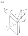
- Fig. 9 shows a schematic illustration for elucidating a light-conductance-increasing element according to the invention embodied as a Computer Generated Hologram (CGH) 900.
- the CGH 900 comprises on its light exit side 901 an array of facet areas (not illustrated), each of which comprising a structure which may be calculated by computer in order to achieve the desired beam-deflecting effect, or angular-spread, respectively.
- the CGH 900 generates for incoming light 910 a desired two-dimensional intensity distribution, which is according to Fig. 9 a quadrupole distribution 920, by way of an angle radiation characteristic defined by the respective beam-deflecting structure.
- the Computer Generated Hologram also comprises a substrate 902 being made of a birefringent, optically uniaxial material e.g. crystalline quartz (SiO 2 ), magnesium fluoride (MgF 2 ), lanthanum fluoride (LaF 3 ) or sapphire (Al 2 O 3 ).
- a birefringent, optically uniaxial material e.g. crystalline quartz (SiO 2 ), magnesium fluoride (MgF 2 ), lanthanum fluoride (LaF 3 ) or sapphire (Al 2 O 3 ).
- the preferred direction of the light-conductance-increasing element if realized as the CGH 900, said preferred direction can be defined here as the direction being oriented from the optical system axis (which is running in Fig. 9 through the center of CGH 900 and along the z-direction) of the illumination device towards an extremum of said two-dimensional intensity distribution (i.e. in the example of Fig.
- the optical crystal axis of said crystal material of the substrate 902 is either substantially parallel or substantially perpendicular to said preferred direction.
- a possible orientation of the optical crystal axis oa in the optically uniaxial material of the substrate 902 is illustrated in Fig. 9 by the broken arrow.
- a further possible direction is perpendicular to said illustrated direction in the x-y-plane.
- said array of facet areas can be formed such that said structures of said Computer Generated Hologram (CGH) comprise no discontinuity across a border between adjacent facet areas.
- the structures provided in the individual facet areas of the Computer Generated Hologram (CGH) behave substantially continuous across borders between adjacent facet areas.
- discontinuities e.g. edges, breaks or the like
- said array of facet areas can be formed such that said structures of said Computer Generated Hologram (CGH) comprise a discontinuity across a border between adjacent facet areas, which may be useful in providing a greater freedom of design.
- the array of facet areas can be formed such that said structures of said Computer Generated Hologram (CGH) are replicated in no one of said facet areas, which may be useful in order to avoid repeated undesired intensity variations by interaction of structures belonging to different facet areas.
- the array of facet areas can be formed such that said structures of said Computer Generated Hologram (CGH) are replicated in at least one facet area of said facet areas.
- Fig. 10 shows, in a schematic illustration, a microlithography projection exposure apparatus 133 comprising a light source unit 135, an illumination device 139, a structure-carrying mask 153, a projection objective 155 and a substrate 159 to be exposed.
- the light source unit 135 may comprise, as light source, for example an ArF laser for an operating wavelength of 193 nm and also a beam shaping optic that generates a parallel light bundle.
- the parallel light bundle firstly impinges on a light-conductance-increasing element 137, which generates a desired intensity distribution, e.g. dipole or quadrupole distribution, by means of the respective diffractively or refractively beam-deflecting structure in a pupil plane 145 and which may be configured as described in the embodiments illustrated above.
- a zoom objective 140 is situated downstream of the light-conductance-increasing element 137 in the light propagation direction, and generates a parallel light bundle with a variable diameter.
- the parallel light bundle is directed onto an optical unit 142 by means of a deflection mirror 141, said optical unit having an axicon 143.
- the optical unit 142 comprises, downstream of the axicon 143, a light mixing system 148 arranged in the region of the pupil plane 145, which light mixing system in this case has, in a manner known per se, an arrangement of micro-optical elements (represented by the elements 146 and 147 in Fig. 10) suitable for obtaining light mixing.
- the light mixing system 148 may alternatively also be a fly's eye condenser or a rod integrator composed of material transparent to light having the operating wavelength, such as e.g.
- the optical unit 142 is followed by a reticle masking system (REMA) 149, which is imaged onto the structure-carrying mask (reticle) 153 by means of a REMA objective 151 and thereby delimits the illuminated region on the reticle 153.
- the structure carrying mask 153 is imaged onto a light-sensitive substrate 159 by means of a projection objective 155.
- an immersion liquid 161 having a different refractive index from that of air is situated between a last optical element 157 of the projection objective 155 and the light-sensitive substrate 159.
Landscapes
- Physics & Mathematics (AREA)
- General Physics & Mathematics (AREA)
- Optics & Photonics (AREA)
- Health & Medical Sciences (AREA)
- Public Health (AREA)
- Epidemiology (AREA)
- Environmental & Geological Engineering (AREA)
- Engineering & Computer Science (AREA)
- Toxicology (AREA)
- Chemical & Material Sciences (AREA)
- Crystallography & Structural Chemistry (AREA)
- Spectroscopy & Molecular Physics (AREA)
- Exposure And Positioning Against Photoresist Photosensitive Materials (AREA)
- Holo Graphy (AREA)
- Exposure Of Semiconductors, Excluding Electron Or Ion Beam Exposure (AREA)
- Optical Elements Other Than Lenses (AREA)
Abstract
Description
- The invention relates to an optical system of an illumination device of a microlithographic projection exposure apparatus, comprising at least one light-conductance-increasing element, in which a generation of light conductance is made possible whilst maintaining the polarization state.
- In an illumination device of a microlithographic projection exposure apparatus, diffractive optical elements (DOEs) are often used particularly at the entrance in order to produce a desired intensity distribution (e.g. dipole or quadrupole distribution) by means of an angular emission characteristic of the DOE that is defined by the respective diffracting surface structure, e.g. in a pupil plane.
- When used in ranges of high energy density of the laser beam, the material of the DOE is subjected to very great loading. With the use of a DOE composed of quartz glass, the short-wave laser light leads to so-called compacting, i.e. local density changes and local anisotropies in the material. A further nondeterministic birefringence distribution is finally established also owing to absorption and the associated heat input and the resultant strains of the material, and destroys the polarization state of the laser light, which can then only be avoided by exchanging the DOE.
- A destruction of the polarization state of the laser light can also result when the DOE is formed from isotropic crystal material, owing to crystal structural defects, stress-induced and/or intrinsic birefringence.
- It is an object of the present invention to provide an optical system of an illumination device of a microlithographic projection exposure apparatus, which enables a generation of light conductance without destroying the polarization state.
- An optical system according to the invention has at least one first light-conductance-increasing element having a plurality of diffractively or refractively beam-deflecting structures extending in a common first preferred direction, the light-conductance-increasing element having an optically uniaxial crystal material in such a way that the optical crystal axis of said crystal material is substantially parallel or substantially perpendicular to the first preferred direction.
- The "light conductance" is also referred to "etendue".
- Owing to the use of crystalline material, what is achieved first of all is that (unlike for instance when using quartz glass) no instances of compacting or strains arise on account of the forces acting between the ions situated at predetermined lattice sites, with the result that no compacting-dictated destruction of the polarization state takes place even in the event of high irradiation loadings. Furthermore the use of optically uniaxial crystal material has the consequence that the permanent birefringence tensor provided by such a crystal material is considerably greater (typically by at least a factor of 102 to 103) than the birefringence tensor generated e.g. by crystal structural defects, with the result that the polarization state is practically no longer disturbed by anisotropies such as crystal structural defects, intrinsic or stress-induced birefringence.
- In particular, according to the invention, the birefringent material is preferably used such that it is irradiated with characteristic states with regard to the polarization, and the deflecting (diffractive or refractive) structures are arranged parallel or perpendicular to the characteristic states. What is thereby achieved is that the induced birefringence effects play no or only a secondary part with regard to polarization.
- The formulation "substantially parallel" or "substantially perpendicular" should be understood in the sense of the present application to mean that, according to the invention, slight deviations from the exact parallel or perpendicular positioning (e.g. deviations of a few degree, more preferably in the order of 1°) are also still possible and are encompassed by the present application.
- Preferably, the beam-deflecting structures are formed on a substrate composed of optically uniaxial crystal material, the optical crystal axis of said crystal material being oriented substantially parallel to the substrate surface.
- According to an embodiment, the plurality of beam-deflecting structures of the first light-conductance-increasing element is formed by an arrangement of cylindrical lenses. According to a further embodiment, the plurality of beam-deflecting structures of the first light-conductance-increasing element can be formed by a diffractive optical element (DOE).
- In particular, the diffractive optical element (DOE) can be a Computer Generated Hologram (CGH). This Computer Generated Hologram (CGH) can comprise an array of facet areas. Each of said facet areas can comprise a structure which may be calculated by computer in order to achieve the desired beam-deflecting effect, or angular-spread, respectively. The Computer Generated Hologram (CGH) also comprises a substrate being made of a birefringent, optically uniaxial material.
- The diffractive optical element (DOE), in particular a Computer Generated Hologram (CGH), may generate a desired two-dimensional intensity distribution (which may in particular have a n-fold symmetry, as given for example in dipole or quadrupole distribution) by way of an angle radiation characteristic defined by the respective beam-deflecting structure. As to the preferred direction of the light-conductance-increasing element chosen according to the present invention, this preferred direction can be defined, in the case of a Computer Generated Hologram (CGH), as the direction being oriented from the optical system axis of the illumination device towards an extremum of said two-dimensional intensity distribution. With other words, the preferred direction may also be defined, if applied to a Computer Generated Hologram (CGH), not on the basis of the specific surface structure of the CGH, but on the basis of the beam deflecting effect which is achieved due to this surface structure. Accordingly, the optical crystal axis of said crystal material of the substrate is either substantially parallel or substantially perpendicular to said preferred direction.
- According to an embodiment, said array of facet areas can be formed such that said structures of said Computer Generated Hologram (CGH) comprise no discontinuity across a border between adjacent facet areas, as disclosed e.g. in
US 5,850,300 and with the advantages described therein. With other words, the structures provided in the individual facet areas of the Computer Generated Hologram (CGH) behave substantially continuous across borders between adjacent facet areas. By avoiding discontinuities (e.g. edges, breaks or the like) between adjacent facet areas, a continuous transition of the phase function can be provided at the borders between the adjacent facet areas, thereby eliminating intensity variations to occur at such borders. - According to a further embodiment, said array of facet areas can be formed such that said structures of said Computer Generated Hologram (CGH) comprise a discontinuity across a border between adjacent facet areas, which may e.g. be useful in providing a greater freedom of design.
- According to an embodiment, said array of facet areas is formed such that said structures of said Computer Generated Hologram (CGH) are replicated in no one of said facet areas, which may be useful in order to avoid repeated undesired intensity variations by interaction of structures belonging to different facet areas.
- According to a further embodiment, said array of facet areas can be formed such that said structures of said Computer Generated Hologram (CGH) are replicated in at least one facet area of said facet areas.
- According to an embodiment, said facet areas have a polygonal shape and are arranged pairwise adjacent to each other. This polygonal shape can particularly be selected from the group consisting of triangle, rectangle, square and hexagon.
- According to an embodiment, facet areas being adjacent to each other have different cross-sections, which may be useful in order to avoid repeated undesired intensity variations by interaction of structures belonging to different facet areas.
- According to a further embodiment, facet areas being adjacent to each other are alike with regard to their cross-section.
- According to an embodiment, the diffractive optical element (DOE) is formed in such a way that the blaze effect is greater for one of two mutually perpendicular polarization states than for the other of said polarization states. According to an embodiment, said two mutually perpendicular polarization states are s-polarization and p-polarization. According to an embodiment, the s-polarized component of light impinging on the diffractive optical element (DOE) is predominantly directed into the ± 1st order of diffraction and the p-polarized component of light impinging on the diffractive optical element (DOE) is predominantly directed into the zeroth order of diffraction.
- According to an embodiment, the optically uniaxial crystal material is a non-optically-active material.
- According to an embodiment, the optically uniaxial crystal material is an optically active material which is present both in a levorotatory and in a dextrorotatory form.
- According to an embodiment, the optically uniaxial crystal material has a fluoride compound.
- According to an embodiment, the optically uniaxial crystal material has a nitride compound.
- According to an embodiment, the optically uniaxial crystal material has an oxide compound.
- The optically uniaxial crystal material may be selected, in particular, from the group containing crystalline quartz (SiO2), magnesium fluoride (MgF2), lanthanum fluoride (LaF3) and sapphire (Al2O3).
- In accordance with one preferred embodiment, a second light-conductance-increasing element is disposed downstream of the first light-conductance-increasing element in the light propagation direction, and has a plurality of diffractively or refractively beam-deflecting structures extending in a second preferred direction, the second preferred direction being different from the first preferred direction.
- In this case, the second preferred direction is substantially perpendicular to the first preferred direction.
- According to an embodiment, the second light-conductance-increasing element is produced from an optically isotropic material at least in the region of the beam-deflecting structures. In particular, the beam-deflecting structures (e.g. cylindrical lenses) may be produced from an optically isotropic material.
- The isotropic material may be selected, in particular, from the group containing calcium fluoride (CaF2), strontium fluoride (SrF2), magnesium oxide (MgO) and YAG. The isotropic material may furthermore also be an amorphous material, in particular quartz glass.
- In accordance with one preferred embodiment, the beam-deflecting structures of the second light-conductance-increasing element are formed on a substrate composed of optically uniaxial crystal material. In this case, the optical crystal axis of said crystal material is preferably oriented substantially parallel to the substrate surface.
- Preferably, the optical crystal axis of the crystal material of the second light-conductance-increasing element is substantially parallel or substantially perpendicular to the second preferred direction.
- The plurality of beam-deflecting structures of the second light-conductance-increasing element may be formed both by an arrangement of cylindrical lenses and by a diffractive optical element.
- According to an embodiment, a first light mixing device is arranged between the first light-conductance-increasing element and the second light-conductance-increasing element.
- According to an embodiment, the first light mixing device is an integrator rod.
- According to an embodiment, the first light-conductance-increasing element can be arranged at a light entrance surface of the integrator rod.
- According to an embodiment, at least one second light mixing device is arranged on that side of the second light-conductance-increasing element which is remote from the first light-conductance-increasing element.
- According to an embodiment, the second light mixing device is an integrator rod.
- According to an embodiment, the second light mixing device comprises a plurality of integrator rods which are arranged successively in the light propagation direction and between which a light-conductance-increasing element is in each case arranged.
- According to an embodiment at least one integrator rod of the first integrator rod, the second integrator rod and the further integrator rods is produced from a birefringent material, in particular quartz (SiO2), magnesium fluoride (MgF2), lanthanum fluoride (LaF3) or sapphire (Al2O3).
- The invention also relates to a diffractive optical element comprising at least one first blaze grating and a second blaze grating, the second blaze grating being superimposed on a light exit surface of the first blaze grating and having a substantially ribbed arrangement of substructures which are smaller than an operating wavelength for which the diffractive optical element (DOE) is designed, characterized in that the diffractive optical element has an optically uniaxial crystal material, the optical crystal axis of said crystal material being substantially parallel or substantially perpendicular to grating structures of the first and/or the second blaze grating.
- According to an embodiment the optically uniaxial crystal material has a fluoride compound.
- According to an embodiment the optically uniaxial crystal material has a nitride compound.
- According to an embodiment the optically uniaxial crystal material has a non-semiconducting oxide compound.
- According to an embodiment the optically uniaxial crystal material has a refractive index n of at least 1.6 at an operating wavelength for which the optical system is designed.
- The invention also relates to a diffractive optical element, a microlithographic projection exposure apparatus, a method for the microlithographic production of microstructured components, and a microstructured component.
- Further configurations of the invention can be gathered from the description and from the subclaims.
- The invention is explained in more detail below on the basis of exemplary embodiments illustrated in the accompanying figures.
- In the drawings:
- Figure 1
- shows a light-conductance-increasing element in accordance with a first embodiment of the invention;
- Figure 2
- shows a light-conductance-increasing element in accordance with a further embodiment of the invention;
- Figure 3
- shows an arrangement according to the invention comprising a first and a second light-conductance-increasing element in accordance with one preferred embodiment;
- Figure 4
- shows a further embodiment, in which a first and a second light-conductive-increasing element are arranged on a common carrier;
- Figure 5
- shows an optical system according to the invention with an integrator rod arranged between a first and second light-conductance-increasing element;
- Figure 6
- shows a further embodiment with a plurality of successively arranged light-conductance-increasing elements and integrator rods;
- Figure 7a-c
- show schematic illustrations for elucidating preferred embodiments of an optical system according to the invention with the use of DOEs;
- Figure 8a-e
- show schematic illustrations for elucidating possible configurations of DOEs used according to the invention;
- Figure 9
- shows a schematic illustration for elucidating a light-conductance-increasing element according to the invention embodied as a CGH; and
- Figure 10
- shows the construction of a microlithography projection exposure apparatus in which an optical system according to the invention is used.
- Fig. 1 shows a light-conductance-increasing
element 100 in accordance with a first embodiment of the present invention. - The
element 100 in accordance with Fig. 1 is formed from acarrier plate 110 composed of optically uniaxial, birefringent crystal material, which is magnesium fluoride (MgF2) in accordance with the exemplary embodiment. - Situated on the light exit surface of the
carrier plate 110 is a plurality of beam-deflectingstructures 120, which, in accordance with the exemplary embodiment, is formed by an arrangement ofcylindrical lenses 121, in such a way that the direction (designated by "D" in Fig. 1) of the longitudinal axes of saidcylindrical lenses 121 is parallel to one another and also parallel to the optical crystal axis - designated by "oa" - of the optically uniaxial crystal material of thecarrier plate 110. - The
cylindrical lenses 121 of theelement 100 are likewise produced on an optically uniaxial crystal material, namely composed of magnesium fluoride (MgF2) in accordance with the exemplary embodiment. Instead of the MgF2 used, it is also possible to use another suitable optically uniaxial crystal material as material for thecarrier plate 110 or thecylindrical lenses 121, for example crystalline quartz (SiO2), lanthanum fluoride (LaF3) and sapphire (Al2O3). The optical activity must be taken into consideration when using crystalline quartz. If the crystal axis is oriented in the plate or substrate plane and illumination is effected in a collimated manner perpendicular to the plate or substrate plane, there is no effect. In all other cases, the harmful effect can also be prevented by combination of levorotatory and dextrorotatory quartz. - The
carrier plate 110 and thecylindrical lenses 121 may comprise the same crystal material or else different crystal materials. Furthermore, thecylindrical lenses 121 may also have a planoconcave form instead of the planoconvex form shown in Fig. 1, and may furthermore also be arranged alternatively at the light entrance surface of thecarrier plate 110. - The
element 100 in accordance with Fig. 1 serves for use in an optical system, in particular in an illumination device of a microlithographic projection exposure apparatus (not illustrated in Fig. 1), a light propagation direction of the light impinging on theelement 100 being indicated on the basis of thearrow 130 in Fig. 1. Furthermore, thearrow 131 is used to designate the preferred direction of polarization of said light, i.e. in the case of linearly polarized light the direction of vibration of the electric field vector E. In the exemplary embodiment, said preferred direction of polarization runs parallel to the optical crystal axis "oa". In accordance with an equally preferred embodiment, as is indicated by the dashedarrow 132, the direction of polarization may also be oriented perpendicular to the optical crystal axis "oa". - A light-conductance-increasing
optical element 200 illustrated in Fig. 2 corresponds to theelement 100 illustrated in Fig. 1, corresponding elements having been designed by reference numerals increased by 100. Theelement 200 differs from theelement 100 only by virtue of the fact that the optical crystal axis "oa" of the material of thecarrier plate 210 runs perpendicular to the direction - designated by "D" - of the longitudinal axes of thecylindrical lenses 221. - In accordance with Fig. 3, an
optical system 300 in accordance with a further preferred embodiment of the invention comprises, in addition to a first light-conductance-increasingelement 300a (the construction of which in the exemplary embodiment corresponds to that from Fig. 1), a second light-conductance-increasingelement 300b. Thefirst element 300a has, at the light exit surface of acarrier plate 310, a plurality ofcylindrical lenses 321 whose longitudinal axis (designed by "D1" in Fig. 3), as in Fig. 1, is parallel to the optical crystal axis "oa-1" of the crystal material of thecarrier plate 310. Like the first light-conductance-increasingelement 300a, the second light-conductance-increasingelement 300b comprises acarrier plate 330 composed of optically uniaxial crystalline material (for example MgF2) whose optical crystal axis "oa-2" is parallel to the optical crystal axis "oa-1" of the crystal material of thefirst carrier plate 310. Situated at the light exit surface of thecarrier plate 330 of thesecond element 300b is anarrangement 340 ofcylindrical lenses 341, the orientation (designated by "D2" in Fig. 3) of the longitudinal axes of saidcylindrical lenses 341 being perpendicular to the orientation "D1" of thecylindrical lenses 321. Consequently, theoptical system 300 comprises, in particular, mutually crossedarrangements cylindrical lenses - In contrast to the
cylindrical lenses 321 of thearrangement 320, however, thecylindrical lenses 341 of thearrangement 340 do not comprise optically uniaxial crystal material, but rather are composed of optically isotropic material, in particular cubically crystalline material. In accordance with the exemplary embodiment, said optically isotropic material is calcium fluoride (CaF2), but it is also possible to use another material transparent at the operating wavelength, for example strontium fluoride (SrF2), magnesium oxide (MgO) or YAG. Furthermore, in an alternative embodiment, an amorphous material, in particular quartz glass, may also be used as the optically isotropic material. - It goes without saying that the
arrangements cylindrical lenses respective carrier plate - In a further exemplary embodiment illustrated in Fig. 4, crossed
cylindrical lens arrangements cylindrical lenses common carrier plate 410. The material of thecarrier plate 410 is once again an optically uniaxial crystal material (for example MgF2), the optical crystal axis "oa" in the exemplary embodiment being parallel to the orientation "D1" of the longitudinal axes of thecylindrical lenses 421 and perpendicular to the orientation "D2" of the longitudinal axes of thecylindrical lenses 431. Analogously to Fig. 3, thecylindrical lenses 421 of thefirst arrangement 420 are produced from optically uniaxial crystal material, whereas thecylindrical lenses 431 forming thesecond arrangement 430 are produced from optically isotropic material. - In accordance with Fig. 5, in a further embodiment of an
optical system 500 according to the invention, a first light-conductance-increasingelement 500a is arranged at the light entrance surface of anintegrator rod 520, and a second light-conductance-increasingelement 500b is arranged at the light exit surface of theintegrator rod 520. The construction of the first and second light-conductance-increasingelements elements - The
integrator rod 520 is in turn produced from an optically uniaxial crystal material, for example MgF2. - In the arrangement in accordance with Fig. 5, the first light-conductance-increasing
element 500a brings about an increase in the light conductance in a first spatial direction, namely in the positive and negative y-direction in accordance with the system of coordinates indicated. By means of theintegrator rod 520, light mixing is likewise effected in the y-direction, with the result that only two of the lateral surfaces of the integrator rod 520 (the upper and lower surfaces in Fig. 5) have to be machined in optically plane-parallel fashion. The second light-conductance-increasingelement 500b brings about an increase in the light conductance and also intermixing of the light emerging from theintegrator rod 520 in a second spatial direction (in the positive and negative x-direction in accordance with Fig. 5) perpendicular to the first spatial direction. - In accordance with further exemplary embodiments (not illustrated), further light-conductance-increasing elements may be disposed downstream of the light-conductance-increasing
element 500b shown in Fig. 5, which further light-conductance-increasing elements bring about a further intermixing of the light emerging from thesecond element 500b. - In accordance with Fig. 6, in a further embodiment of an
optical system 600 according to the invention, a first light-conductance-increasingelement 610 is arranged at the light entrance surface of afirst integrator rod 620, and a second light-conductance-increasingelement 630 is arranged at the light exit surface of theintegrator rod 620. The first light-conductance-increasingelement 610 results in an expansion perpendicular to the plane of the drawing (in the positive and negative x-direction in accordance with the system of coordinates indicated in the figure), and the second light-conductance-increasingelement 630 results in aperture generation in the plane of the drawing (i.e. in the positive and negative y-direction). A third light-conductance-increasingelement 640, asecond integrator rod 650, a fourth light-conductance-increasingelement 670 and athird integrator rod 660 are arranged successively downstream of the second light-conductance-increasingelement 630 in the light propagation direction (x-direction). In a generalization of the arrangement of Fig. 6, the light mixing device disposed downstream of the second light-conductance-increasingelement 620 comprises a plurality ofintegrator rods element 670, ... is in each case arranged. In the arrangement of Fig. 6, theintegrator rod 620 is once again preferably produced from an optically uniaxial crystal material, e.g. MgF2, the optical crystal axis "oa", analogously to the embodiment of Fig. 5, once again being parallel to the preferred direction of the beam-deflecting structures of the first light-conductance-increasingelement 610 and perpendicular to the preferred direction of the beam-deflecting structures of the second light-conductance-increasing element 630 (or visa versa). However, unlike in the embodiments described previously, the light-conductance-increasingelement - In contrast to the
integrator rod 620, theintegrator rods - The
optical system 600 shown in Fig. 6 is preferably arranged upstream of the input of a REMA objective present in an illumination device of a microlithographic projection apparatus. - In the embodiments described above, where cylindrical lens arrangements are provided as light-conductance-increasing elements, as an alternative DOEs may also be arranged, and vice versa.
- In accordance with Fig. 7a, it is possible, for instance analogously to the exemplary embodiment shown in Fig. 3, to provide a
corresponding arrangement 710 comprising afirst DOE 712 arranged on afirst carrier 711 and asecond DOE 714 arranged on asecond carrier 713, said second DOE being disposed downstream in the light propagation direction, theDOEs - The DOE may be formed in a known manner by the formation of light-opaque structures on a carrier or in the form of light-transmissive structures in specific regions with a varying refractive index and/or varying geometrical thickness. These structures of a DOE may be performed for example by corresponding material removal in a carrier plate composed of optically uniaxial crystal material. In a further exemplary embodiment, an amorphous layer composed of quartz glass may also be vapor-deposited onto a carrier plate composed of optically uniaxial crystal material, into which layer the patterning is subsequently introduced by etching. The latter embodiment has the advantage that a more uniform formation of the edges present in the structures is possible in the case of patterning of the amorphous layer than in the case of direct patterning of the crystalline carrier plate.
- In the
arrangement 710 of Fig. 7a, the carrier 711 (and thus, in the case of integral formation with the DOE, also the structures of the DOE 712) is produced from optically uniaxial crystal material, e.g. MgF2. In the case of an integral formation of the second light-conductance-increasing element (by forming theDOE 714 by means of material removal in the carrier 713), thecarrier 713 is preferably produced, analogously to the embodiment of Fig. 3, from an optically isotropic material, i.e. either a cubically crystalline material or an amorphous material (e.g. quartz glass). In one preferred embodiment, however thesecond carrier 713 is produced from optically uniaxial crystal material in the same way as the first carrier, and theDOE 714 is produced by vapor deposition and subsequent etching of an amorphous layer, in particular composed of quartz glass. - It goes without saying that the
DOEs carrier - In accordance with Fig. 7b, it is furthermore possible for
DOEs common carrier 721. In thisarrangement 720, thecarrier 721 is produced from an optically uniaxial crystal material, e.g. MgF2, and theDOE 723 arranged at the light exit surface of thecarrier 721 is formed, as described above, by vapor deposition and etching of an amorphous layer composed of e.g. quartz glass. TheDOE 722 arranged at the light entrance surface of thecarrier 721 may optionally be formed from optically uniaxial crystal material (that is say in particular integrally with thecarrier 721 by means of corresponding material removal) or likewise by means of vapor deposition and etching of an amorphous layer composed of e.g. quartz glass. - Furthermore, it is also possible, as indicated in Fig. 7c, to form a more
complex DOE structure 732 with deflection in arbitrary spatial directions on a carrier 731 (once again composed of optically uniaxial crystal material), which structure is once again produced by vapor deposition and etching of an amorphous layer composed of e.g. quartz glass. - In further preferred embodiments, the diffractive optical elements (DOEs) used according to the invention which have an optically uniaxial crystal material as explained above may also be equipped with a blaze effect in order to direct radiation intensity into a desired order of diffraction, in particular for instance the first order of diffraction, in a targeted manner. For this purpose, in a manner known per se, the respective DOE may be formed with a typically sawtooth or stepped profile with corresponding
periodic structures schematic arrangement 800 with reference to Fig. 8a. - In a further preferred embodiment, a DOE according to the invention which has an optically uniaxial crystal material as explained above is formed in polarization-selective fashion in such a way that the blaze effect is greater for one of two mutually perpendicular polarization states (in particular s-polarization and p-polarization) than for the other of said polarization states. By way of example, the DOE may be formed in such a way that the s-polarized component of light impinging on the DOE is predominantly directed into the ± 1st order of diffraction and the p-polarized component of light impinging on the DOE is predominantly directed into the zeroth order of diffraction.
- In accordance with Fig. 8b, a diffractive optical element has a first blaze grating 810 and a second blaze grating 820, the second blaze grating 820 being superimposed on the light exit surface of the first blaze grating 810. In this case, the second blaze grating 820 has an arrangement of
substructures 820a-820e, which can be described as comb-shaped or ribbed, theindividual substructures 820a-820e (which are only illustrated schematically and are typically present in a significantly greater number) being smaller than the operating wavelength (of λ = 193 nm for example) for which the DOE is designed. - In accordance with the exemplary embodiment of Fig. 8b, in the blaze grating 820 having the sub wavelength structuring of
substructures 820a-820e, the filling ratio decreases along the extending direction "D" of said blaze grating 820 from left to right. In this case, the "filling ratio" is to be understood as the ratio of the dimension of thesubstructures 820a-820e in extending direction "D" relative to the period "g" of the blaze grating 820 having the sub wavelength structuring, with the result that the width of thesubstructures 820a-820e within each period of thefirst diffraction grating 810 decreases in the extending direction "D" from left to right in order, given corresponding optimization, to achieve the effect that the s-polarized component of light impinging on the DOE is predominately directed into the first order of diffraction and the p-polarized component of light impinging on the DOE is predominately directed into the zeroth order of diffraction. - The formation of a DOE with a blaze effect in conjunction with a polarization-selective effect with the aim of optimizing the blaze effect only for one of two mutually perpendicular polarization states is not restricted to the
arrangement 850 illustrated schematically in Fig. 8b. Thus, thesubstructures 820a-820e can also be formed uniformly (i.e. with constant width and length) over the period of the second blaze grating 820 in a manner known per se, in order, given corresponding optimization, to obtain a deflection for instance of the s-polarized component into the (±1) st order of diffraction. Furthermore, in a modification of the arrangement shown in Fig. 8b, thesubstructures 820a-820e may also be formed with constant width and variable length (i.e. variable extent perpendicular to the extending direction "D" of the blaze grating 820), e.g. with a length that decreases within each period of thefirst diffraction grating 810 in the extending direction "D" from left to right. - The construction of further possible embodiments of DOEs according to the present invention is illustrated schematically in Fig. 8c-e.
- In accordance with Fig. 8c, by way of example, as illustrated on the basis of a
partial region 860 of a DOE,typical DOE structures partial region 870 of a further DOE,DOE structures substrate 871 composed of e.g. crystalline quartz or sapphire (Al2O3) and which comprise a multilayer composed of layers each comprising an oxide or fluoride compound (e.g. MgF2 or Al2O3). Fig. 8e shows, on the basis of apartial region 880 of a further DOE,integral DOE structures substrate 881 composed of e.g. crystalline quartz or sapphire (Al2O3) and which in each case comprise an oxide or fluoride compound, e.g. calcium fluoride (CaF2). - The optical crystal axis of the optically uniaxial crystal material respectively used, in particular in the substrate (that is to say for example the crystalline quartz), is parallel to the substrate surface. Preferably, the optical crystal axis of the optically uniaxial crystal material respectively used in the substrate is, moreover, parallel or perpendicular to the preferred direction of the beam-deflecting structures, and furthermore parallel or perpendicular to the preferred direction of polarization of light impinging on the light-conductance-increasing element. Furthermore, the substrate preferably has a thickness which is an integral multiple of the operating wavelength used (e.g. 193 nm or 157 nm).
- Fig. 9 shows a schematic illustration for elucidating a light-conductance-increasing element according to the invention embodied as a Computer Generated Hologram (CGH) 900. The
CGH 900 comprises on itslight exit side 901 an array of facet areas (not illustrated), each of which comprising a structure which may be calculated by computer in order to achieve the desired beam-deflecting effect, or angular-spread, respectively. - The
CGH 900 generates for incoming light 910 a desired two-dimensional intensity distribution, which is according to Fig. 9 aquadrupole distribution 920, by way of an angle radiation characteristic defined by the respective beam-deflecting structure. - The Computer Generated Hologram (CGH) also comprises a
substrate 902 being made of a birefringent, optically uniaxial material e.g. crystalline quartz (SiO2), magnesium fluoride (MgF2), lanthanum fluoride (LaF3) or sapphire (Al2O3). As to the preferred direction of the light-conductance-increasing element if realized as theCGH 900, said preferred direction can be defined here as the direction being oriented from the optical system axis (which is running in Fig. 9 through the center ofCGH 900 and along the z-direction) of the illumination device towards an extremum of said two-dimensional intensity distribution (i.e. in the example of Fig. 9 from the center of thequadrupole distribution 920 to one of the four poles of the quadrupole distribution 920), i.e. along a diagonal line in the square defined by saidquadrupole distribution 920. The optical crystal axis of said crystal material of thesubstrate 902 is either substantially parallel or substantially perpendicular to said preferred direction. A possible orientation of the optical crystal axis oa in the optically uniaxial material of thesubstrate 902 is illustrated in Fig. 9 by the broken arrow. A further possible direction is perpendicular to said illustrated direction in the x-y-plane. - According to an embodiment, said array of facet areas can be formed such that said structures of said Computer Generated Hologram (CGH) comprise no discontinuity across a border between adjacent facet areas. With other words, the structures provided in the individual facet areas of the Computer Generated Hologram (CGH) behave substantially continuous across borders between adjacent facet areas. By avoiding discontinuities (e.g. edges, breaks or the like) between adjacent facet areas, a continuous transition of the phase function can be provided at the borders between the adjacent facet areas, thereby eliminating intensity variations to occur at such borders. According to a further embodiment, said array of facet areas can be formed such that said structures of said Computer Generated Hologram (CGH) comprise a discontinuity across a border between adjacent facet areas, which may be useful in providing a greater freedom of design.
- Furthermore, the array of facet areas can be formed such that said structures of said Computer Generated Hologram (CGH) are replicated in no one of said facet areas, which may be useful in order to avoid repeated undesired intensity variations by interaction of structures belonging to different facet areas. Alternatively, the array of facet areas can be formed such that said structures of said Computer Generated Hologram (CGH) are replicated in at least one facet area of said facet areas.
- Fig. 10 shows, in a schematic illustration, a microlithography
projection exposure apparatus 133 comprising alight source unit 135, anillumination device 139, a structure-carryingmask 153, aprojection objective 155 and asubstrate 159 to be exposed. Thelight source unit 135 may comprise, as light source, for example an ArF laser for an operating wavelength of 193 nm and also a beam shaping optic that generates a parallel light bundle. - In accordance with the exemplary embodiment, the parallel light bundle firstly impinges on a light-conductance-increasing
element 137, which generates a desired intensity distribution, e.g. dipole or quadrupole distribution, by means of the respective diffractively or refractively beam-deflecting structure in apupil plane 145 and which may be configured as described in the embodiments illustrated above. Azoom objective 140 is situated downstream of the light-conductance-increasingelement 137 in the light propagation direction, and generates a parallel light bundle with a variable diameter. The parallel light bundle is directed onto anoptical unit 142 by means of adeflection mirror 141, said optical unit having anaxicon 143. By means of thezoom objective 140 in conjunction with the upstream light-conductance-increasingelement 137 and theaxicon 143, different illumination configurations are generated in thepupil plane 145 depending on zoom setting and position of the axicon elements. Theoptical unit 142 comprises, downstream of theaxicon 143, alight mixing system 148 arranged in the region of thepupil plane 145, which light mixing system in this case has, in a manner known per se, an arrangement of micro-optical elements (represented by theelements light mixing system 148 may alternatively also be a fly's eye condenser or a rod integrator composed of material transparent to light having the operating wavelength, such as e.g. quartz glass or else crystalline calcium fluoride. Theoptical unit 142 is followed by a reticle masking system (REMA) 149, which is imaged onto the structure-carrying mask (reticle) 153 by means of aREMA objective 151 and thereby delimits the illuminated region on thereticle 153. Thestructure carrying mask 153 is imaged onto a light-sensitive substrate 159 by means of aprojection objective 155. In the exemplary embodiment illustrated, animmersion liquid 161 having a different refractive index from that of air is situated between a lastoptical element 157 of theprojection objective 155 and the light-sensitive substrate 159. - Even though the invention has been described on the basis of specific embodiments, numerous variations and alternative embodiments can be deduced by the person skilled in the art, e.g. by combination and/or exchange of features of individual embodiments. Accordingly, it goes without saying for the person skilled in the art that such variations and alternative embodiments are also encompassed by the present invention, and the scope of the invention is only restricted within the meaning of the accompanying patent claims and the equivalents thereof.
Claims (44)
- An optical system of an illumination device of a microlithographic projection exposure apparatus, comprising:• at least one first light-conductance-increasing element (100, 200, 300a, 400, 500a, 900) having a plurality of diffractively or refractively beam-deflecting structures extending in a common first preferred direction (D1);• the light-conductance-increasing element having an optically uniaxial crystal material in such a way that the optical crystal axis of said crystal material is substantially parallel or substantially perpendicular to the first preferred direction (D1).
- The optical system according to Claim 1, characterized in that the light-conductance-increasing element is arranged in such a way that the optical crystal axis is substantially parallel or substantially perpendicular to the preferred direction of polarization of light impinging on the light-conductance-increasing element.
- The optical system according to Claim 1 or 2, characterized in that the beam-deflecting structures are formed on a substrate composed of optically uniaxial crystal material, the optical crystal axis of said crystal material being oriented substantially parallel to the substrate surface.
- The optical system according to anyone of the Claims 1 to 3, characterized in that the plurality of beam-deflecting structures of the first light-conductance-increasing element is formed by an arrangement of cylindrical lenses (121, 221, 321, 421, 511).
- The optical system according to anyone of the Claims 1 to 3, characterized in that the plurality of beam-deflecting structures of the first light-conductance-increasing element is formed by a diffractive optical element (DOE).
- The optical system according to Claim 5, characterized in that said diffractive optical element (DOE) is a Computer Generated Hologram (CGH).
- The optical system according to Claim 6, characterized in that said Computer Generated Hologram (CGH) comprises an array of facet areas.
- The optical system according to Claim 7, characterized in that said array of facet areas is formed such that said beam-deflecting structures of said Computer Generated Hologram (CGH) comprise a discontinuity across a border between adjacent facet areas.
- The optical system according to Claim 7, characterized in that said array of facet areas is formed such that said beam-deflecting structures of said Computer Generated Hologram (CGH) comprise no discontinuity across a border between adjacent facet areas.
- The optical system according to anyone of the Claims 7 to 9, characterized in that said array of facet areas is formed such that said beam-deflecting structures of said Computer Generated Hologram (CGH) are replicated in at least one facet area of said facet areas.
- The optical system according to anyone of the Claims 7 to 9, characterized in that said array of facet areas is formed such that said beam-deflecting structures of said Computer Generated Hologram (CGH) are replicated in no one of said facet areas.
- The optical system according to anyone of the Claims 7 to 11, characterized in that said facet areas have a polygonal shape and are arranged pairwise adjacent to each other.
- The optical system according to Claim 12, characterized in that said polygonal shape is selected from the group consisting of triangle, rectangle, square and hexagon.
- The optical system according to anyone of the Claims 7 to 13, characterized in that facet areas being adjacent to each other are alike with regard to their cross-section.
- The optical system according to anyone of the Claims 7 to 13, characterized in that facet areas being adjacent to each other have different cross-sections.
- The optical system according to Claim 5, characterized in that said diffractive optical element (DOE) has at least one blaze grating.
- The optical system according to Claim 16, characterized in that said diffractive optical element (DOE) is formed in such a way that the blaze effect is greater for one of two mutually perpendicular polarization states than for the other of said polarization states.
- The optical system according to Claim 16 or 17, characterized in that the diffractive optical element (DOE) has a first blaze grating (810) and at least one second blaze grating (820), grating structures of at least one of said blaze gratings being smaller than an operating wavelength for which the diffractive optical element (DOE) is designed.
- The optical system according to Claim 18, characterized in that the grating structures of the second blaze grating (820) are formed on the first blaze grating (810).
- The optical system according to Claim 19, characterized in that the second blaze grating (820) is superimposed on a light exit surface of the first blaze grating (810).
- The optical system according to anyone of the Claims 18 to 20, characterized in that at least one of said blaze gratings (820) has a substantially ribbed structure.
- The optical system according to anyone of the Claims 18 to 21, characterized in that the first blaze grating (810) has a substantially stepped or a substantially sawtooth-shaped geometry.
- The optical system according to anyone of the Claims 18 to 22, characterized in that the second blaze grating (820) is formed from substructures (820a-820e) which are arranged alongside one another along an extending direction (D) and are smaller than an operating wavelength for which the diffractive optical element (DOE) is designed.
- The optical system according to Claim 23, characterized in that said substructures (820a-820e) are formed on the substantially stepped or substantially sawtooth-shaped sections of the first blaze grating (810).
- The optical system according to Claim 23 or 24, characterized in that the arrangement of said substructures (820a-820e) varies in said extending direction (D).
- The optical system according to anyone of the Claims 23 to 25, characterized in that the arrangement of said substructures (820a-820e) varies perpendicular to the extending direction (D).
- The optical system according to anyone of the Claims 23 to 26, characterized in that the filling ratio of said substructures (820a-820e) is constant along the extending direction (D).
- The optical system according to anyone of the preceding claims, characterized in that a second light-conductance-increasing element (300b, 500b) is disposed downstream of the first light-conductance-increasing element (300a, 500a) in the light propagation direction, and has a plurality of diffractively or refractively beam-deflecting structures extending in a second preferred direction (D2), the second preferred direction (D2) being different from the first preferred direction (D1).
- The optical system according to Claim 28, characterized in that the second preferred direction (D2) is substantially perpendicular to the first preferred direction (D1).
- The optical system according to Claim 28 or 29, characterized in that the second light-conductance-increasing element (300b, 500b) is produced from an optically isotropic material at least in the region of the beam-deflecting structures.
- The optical system according to anyone of the Claims 28 to 30, characterized in that the beam-deflecting structures of the second light-conductance-increasing element (300b, 500b) are formed on a substrate composed of optically uniaxial crystal material (530).
- The optical system according to anyone of the Claims 28 to 31, characterized in that the optical crystal axis of a crystal material of the second light-conductance-increasing element is substantially parallel or substantially perpendicular to the second preferred direction.
- The optical system according to anyone of the Claims 28 to 32, characterized in that a first light mixing device is arranged between the first light-conductance-increasing element (500a) and the second light-conductance-increasing element (500b).
- The optical system according to Claim 33, characterized in that at least one second light mixing device is arranged on that side of the second light-conductance-increasing element which is remote from the first light-conductance-increasing element.
- The optical system according to anyone of the preceding claims, characterized in that an operating wavelength for which the optical system is designed is less than 250 nm, preferably less than 200 nm, and even more preferably less than 160 nm.
- The optical system according to anyone of the preceding claims, characterized in that at least one light-conductance-increasing element has a substrate composed of an optically uniaxial crystal material having a thickness that is an integral multiple of the operating wavelength used.
- A diffractive optical element comprising at least one first blaze grating (810) and a second blaze grating (820), the second blaze grating (820) being superimposed on a light exit surface of the first blaze grating (810) and having a substantially ribbed arrangement of substructures (820a, 820e) which are smaller than an operating wavelength for which the diffractive optical element (DOE) is designed, characterized in that the diffractive optical element has an optically uniaxial crystal material, the optical crystal axis of said crystal material being substantially parallel or substantially perpendicular to grating structures of the first and/or the second blaze grating.
- The diffractive optical element according to Claim 37, characterized in that the optically uniaxial crystal material has a refractive index n of at least 1.6 at an operating wavelength for which the optical system is designed.
- A diffractive optical element comprising at least one first blaze grating (810) and a second blaze grating (820), the second blaze grating (820) being superimposed on a light exit surface of the first blaze grating (810) and having a substantially ribbed arrangement of substructures (820a-820e) which are smaller than an operating wavelength for which the diffractive optical element (DOE) is designed, characterized in that the diffractive optical element has an optically uniaxial crystal material which is selected from the group containing magnesium fluoride (MgF2), lanthanum fluoride (LaF3) and sapphire (Al2O3).
- A diffractive optical element comprising at least one first blaze grating (810) and a second blaze grating (820), the second blaze grating (820) being superimposed on a light exit surface of the first blaze grating (810) and having a substantially ribbed arrangement of substructures (820a-820e) which are smaller than an operating wavelength for which the diffractive optical element (DOE) is designed, characterized in that the diffractive optical element has a naturally birefringent, non-optically active crystal material.
- An illumination device of a microlithographic projection exposure apparatus, characterized in that it has an optical system according to anyone of the Claims 1 to 36 and/or a diffractive optical element according to anyone of the Claims 37 to 40.
- A microlithographic projection exposure apparatus (133), having an illumination device (139) according to Claim 41.
- A method for the microlithographic production of microstructured components, having the following steps:• providing a substrate (159), to which a layer composed of a light-sensitive material is at least partially applied;• providing a mask (153) having structures to be imaged;• providing a projection exposure apparatus (133) according to Claim 42;• projecting at least one part of the mask (153) onto a region of the layer with the aid of the projection exposure apparatus (133).
- A microstructured component produced by a method according to Claim 43.
Applications Claiming Priority (2)
| Application Number | Priority Date | Filing Date | Title |
|---|---|---|---|
| US78208906P | 2006-03-14 | 2006-03-14 | |
| DE102006012034A DE102006012034A1 (en) | 2006-03-14 | 2006-03-14 | Optical system e.g. lighting device, for use in microlithographic projection lighting system, has light-conductance-increasing unit with set of diffractive or refractive beam deflecting structures extending in common direction |
Publications (3)
| Publication Number | Publication Date |
|---|---|
| EP1835312A2 true EP1835312A2 (en) | 2007-09-19 |
| EP1835312A3 EP1835312A3 (en) | 2007-10-10 |
| EP1835312B1 EP1835312B1 (en) | 2011-05-04 |
Family
ID=38374829
Family Applications (1)
| Application Number | Title | Priority Date | Filing Date |
|---|---|---|---|
| EP07103867A Ceased EP1835312B1 (en) | 2006-03-14 | 2007-03-09 | Illumination device for a microlithographic projection apparatus having an element made of uniaxial crystal and having a plurality of refractive or diffractive structures extending along an axis being parallel or perpendicular to the crystal axis |
Country Status (4)
| Country | Link |
|---|---|
| US (1) | US8068279B2 (en) |
| EP (1) | EP1835312B1 (en) |
| JP (1) | JP5179077B2 (en) |
| DE (2) | DE102006012034A1 (en) |
Cited By (3)
| Publication number | Priority date | Publication date | Assignee | Title |
|---|---|---|---|---|
| DE102009016608A1 (en) | 2008-05-21 | 2009-11-26 | Carl Zeiss Smt Ag | Illumination optic for a microlithography projection exposure system for illuminating an object field with illumination light of a radiation source, comprises an optical beam forming element, and a group of beam formation sections |
| CN106647179A (en) * | 2016-11-25 | 2017-05-10 | 天津津芯微电子科技有限公司 | Compound-eye light homogenization system, optical engine and light source optimization device |
| WO2022048502A1 (en) * | 2020-09-04 | 2022-03-10 | 宁波舜宇光电信息有限公司 | Optical waveguide apparatus for ar device and method for manufacturing optical waveguide apparatus, and ar device |
Families Citing this family (18)
| Publication number | Priority date | Publication date | Assignee | Title |
|---|---|---|---|---|
| TWI456267B (en) | 2006-02-17 | 2014-10-11 | 卡爾蔡司Smt有限公司 | Lighting system for lithographic projection exposure equipment |
| ATE525679T1 (en) * | 2006-02-17 | 2011-10-15 | Zeiss Carl Smt Gmbh | OPTICAL INTEGRATOR FOR AN ILLUMINATION SYSTEM OF A MICROLITHOGRAPHY PROJECTION EXPOSURE DEVICE |
| JP5078765B2 (en) * | 2008-06-10 | 2012-11-21 | キヤノン株式会社 | Computer generated hologram, exposure apparatus and device manufacturing method |
| JP5078764B2 (en) * | 2008-06-10 | 2012-11-21 | キヤノン株式会社 | Computer generated hologram, exposure apparatus and device manufacturing method |
| JP2011133640A (en) * | 2009-12-24 | 2011-07-07 | Dainippon Printing Co Ltd | Method for producing transmissive hologram |
| WO2012018017A1 (en) * | 2010-08-06 | 2012-02-09 | 旭硝子株式会社 | Diffractive optical element and measurement device |
| US8902485B2 (en) | 2012-11-29 | 2014-12-02 | Christie Digital Systems Usa, Inc. | Contrast enhancing system |
| EP2754524B1 (en) | 2013-01-15 | 2015-11-25 | Corning Laser Technologies GmbH | Method of and apparatus for laser based processing of flat substrates being wafer or glass element using a laser beam line |
| EP2781296B1 (en) | 2013-03-21 | 2020-10-21 | Corning Laser Technologies GmbH | Device and method for cutting out contours from flat substrates using a laser |
| US10293436B2 (en) | 2013-12-17 | 2019-05-21 | Corning Incorporated | Method for rapid laser drilling of holes in glass and products made therefrom |
| US11556039B2 (en) | 2013-12-17 | 2023-01-17 | Corning Incorporated | Electrochromic coated glass articles and methods for laser processing the same |
| KR102445217B1 (en) | 2014-07-08 | 2022-09-20 | 코닝 인코포레이티드 | Method and apparatus for laser processing material |
| LT3169477T (en) * | 2014-07-14 | 2020-05-25 | Corning Incorporated | System for and method of processing transparent materials using laser beam focal lines adjustable in length and diameter |
| WO2016154284A1 (en) | 2015-03-24 | 2016-09-29 | Corning Incorporated | Laser cutting and processing of display glass compositions |
| WO2018064409A1 (en) | 2016-09-30 | 2018-04-05 | Corning Incorporated | Apparatuses and methods for laser processing transparent workpieces using non-axisymmetric beam spots |
| LT3529214T (en) | 2016-10-24 | 2021-02-25 | Corning Incorporated | SUBSTRATE PROCESSING STATION FOR LASER MACHINERY OF SHEET SHAPE GLASS SUBSTRATES |
| WO2020153504A1 (en) * | 2019-01-25 | 2020-07-30 | 大日本印刷株式会社 | Diffractive optical device, illumination apparatus, projection apparatus, projection display apparatus, and method for manufacturing element diffractive optical device |
| DE102024207296A1 (en) * | 2024-08-01 | 2026-02-05 | Carl Zeiss Smt Gmbh | Optical assembly |
Family Cites Families (15)
| Publication number | Priority date | Publication date | Assignee | Title |
|---|---|---|---|---|
| US5610733A (en) | 1994-02-28 | 1997-03-11 | Digital Optics Corporation | Beam-homogenizer |
| US5850300A (en) | 1994-02-28 | 1998-12-15 | Digital Optics Corporation | Diffractive beam homogenizer having free-form fringes |
| JP2000206321A (en) * | 1999-01-19 | 2000-07-28 | Canon Inc | Diffractive optical element, optical system having diffractive optical element, method of manufacturing diffractive optical element, exposure apparatus including optical system having diffractive optical element, and method of manufacturing device using exposure apparatus |
| JP2001343512A (en) * | 2000-05-31 | 2001-12-14 | Canon Inc | Diffractive optical element and optical system having the same |
| DE10124803A1 (en) * | 2001-05-22 | 2002-11-28 | Zeiss Carl | Polarizer and microlithography projection system with polarizer |
| JP4859311B2 (en) * | 2001-09-17 | 2012-01-25 | 株式会社リコー | Laser illumination optical system, exposure apparatus using the optical system, laser processing machine, and projection apparatus |
| JP4310080B2 (en) * | 2002-06-17 | 2009-08-05 | キヤノン株式会社 | Diffractive optical element and optical system and optical apparatus provided with the same |
| JP2005032909A (en) * | 2003-07-10 | 2005-02-03 | Fuji Photo Film Co Ltd | Lighting optical system and aligner using it |
| GB2403815A (en) * | 2003-07-10 | 2005-01-12 | Ocuity Ltd | Birefringent lens array structure |
| DE10344010A1 (en) * | 2003-09-15 | 2005-04-07 | Carl Zeiss Smt Ag | Honeycomb condenser and lighting system with it |
| US20070019179A1 (en) | 2004-01-16 | 2007-01-25 | Damian Fiolka | Polarization-modulating optical element |
| JP4497968B2 (en) * | 2004-03-18 | 2010-07-07 | キヤノン株式会社 | Illumination apparatus, exposure apparatus, and device manufacturing method |
| EP1754111A1 (en) * | 2004-06-10 | 2007-02-21 | Carl Zeiss SMT AG | Lighting unit of a microlithographic projection exposure system |
| DE102005030543A1 (en) * | 2004-07-08 | 2006-02-02 | Carl Zeiss Smt Ag | Polarizer device for illumination system, has interference device converting light beam with angular distribution to another beam, and decoupling device receiving latter beam and emitting beam with another angular distribution |
| DE102005039519A1 (en) | 2005-08-20 | 2007-02-22 | Carl Zeiss Smt Ag | Projection illumination equipment for manufacturing semiconductor component, has cuboid shaped light conducting rod, and crystallographic main axis extending approximately perpendicular or parallel to longitudinal extension of rod |
-
2006
- 2006-03-14 DE DE102006012034A patent/DE102006012034A1/en not_active Withdrawn
-
2007
- 2007-03-09 DE DE602007014285T patent/DE602007014285D1/en active Active
- 2007-03-09 EP EP07103867A patent/EP1835312B1/en not_active Ceased
- 2007-03-13 US US11/685,620 patent/US8068279B2/en active Active
- 2007-03-14 JP JP2007064831A patent/JP5179077B2/en active Active
Cited By (3)
| Publication number | Priority date | Publication date | Assignee | Title |
|---|---|---|---|---|
| DE102009016608A1 (en) | 2008-05-21 | 2009-11-26 | Carl Zeiss Smt Ag | Illumination optic for a microlithography projection exposure system for illuminating an object field with illumination light of a radiation source, comprises an optical beam forming element, and a group of beam formation sections |
| CN106647179A (en) * | 2016-11-25 | 2017-05-10 | 天津津芯微电子科技有限公司 | Compound-eye light homogenization system, optical engine and light source optimization device |
| WO2022048502A1 (en) * | 2020-09-04 | 2022-03-10 | 宁波舜宇光电信息有限公司 | Optical waveguide apparatus for ar device and method for manufacturing optical waveguide apparatus, and ar device |
Also Published As
| Publication number | Publication date |
|---|---|
| JP2007258709A (en) | 2007-10-04 |
| JP5179077B2 (en) | 2013-04-10 |
| DE102006012034A1 (en) | 2007-09-20 |
| US20070217013A1 (en) | 2007-09-20 |
| EP1835312A3 (en) | 2007-10-10 |
| US8068279B2 (en) | 2011-11-29 |
| EP1835312B1 (en) | 2011-05-04 |
| DE602007014285D1 (en) | 2011-06-16 |
Similar Documents
| Publication | Publication Date | Title |
|---|---|---|
| EP1835312B1 (en) | Illumination device for a microlithographic projection apparatus having an element made of uniaxial crystal and having a plurality of refractive or diffractive structures extending along an axis being parallel or perpendicular to the crystal axis | |
| EP2927935B1 (en) | Illumination optical apparatus and projection exposure apparatus | |
| JP4933671B2 (en) | Illumination system for microlithographic projection exposure apparatus | |
| JP5066611B2 (en) | Illumination system for microlithography projection exposure apparatus | |
| JP5935920B2 (en) | Illumination optical system, exposure apparatus, illumination method, exposure method, and device manufacturing method | |
| JP6583741B2 (en) | Illumination optical system, exposure apparatus, and device manufacturing method | |
| TWI293696B (en) | Optical system for spatially controlling ligth polarization and method for manufacturing the same | |
| US8437058B2 (en) | Computer generated hologram and exposure apparatus to suppress an illumination variation and loss in light | |
| JP5566501B2 (en) | In particular, the optical system of a microlithography projection exposure apparatus | |
| JP2016186642A (en) | Polarization-influencing optical arrangement in particular in microlithographic projection exposure apparatus | |
| KR101551991B1 (en) | Illumination system of a microlithographic projection exposure apparatus | |
| JP5369319B2 (en) | Illumination system for microlithography projection exposure apparatus | |
| KR20090006747A (en) | Exposure apparatus, optical element sorting method and device manufacturing method | |
| HK1214033B (en) | Illumination optical apparatus and projection exposure apparatus | |
| WO2007019886A1 (en) | Optical system, namely objective or illumination device of a microlithographic projection exposure system | |
| HK1189426B (en) | Illumination optical apparatus and projection exposure apparatus | |
| HK1189096A (en) | Illumination optical apparatus and projection exposure apparatus |
Legal Events
| Date | Code | Title | Description |
|---|---|---|---|
| PUAI | Public reference made under article 153(3) epc to a published international application that has entered the european phase |
Free format text: ORIGINAL CODE: 0009012 |
|
| PUAL | Search report despatched |
Free format text: ORIGINAL CODE: 0009013 |
|
| AK | Designated contracting states |
Kind code of ref document: A2 Designated state(s): AT BE BG CH CY CZ DE DK EE ES FI FR GB GR HU IE IS IT LI LT LU LV MC MT NL PL PT RO SE SI SK TR |
|
| AX | Request for extension of the european patent |
Extension state: AL BA HR MK YU |
|
| AK | Designated contracting states |
Kind code of ref document: A3 Designated state(s): AT BE BG CH CY CZ DE DK EE ES FI FR GB GR HU IE IS IT LI LT LU LV MC MT NL PL PT RO SE SI SK TR |
|
| AX | Request for extension of the european patent |
Extension state: AL BA HR MK YU |
|
| 17P | Request for examination filed |
Effective date: 20080117 |
|
| 17Q | First examination report despatched |
Effective date: 20080303 |
|
| AKX | Designation fees paid |
Designated state(s): CH DE LI NL |
|
| GRAP | Despatch of communication of intention to grant a patent |
Free format text: ORIGINAL CODE: EPIDOSNIGR1 |
|
| RAP1 | Party data changed (applicant data changed or rights of an application transferred) |
Owner name: CARL ZEISS SMT GMBH |
|
| GRAS | Grant fee paid |
Free format text: ORIGINAL CODE: EPIDOSNIGR3 |
|
| GRAA | (expected) grant |
Free format text: ORIGINAL CODE: 0009210 |
|
| AK | Designated contracting states |
Kind code of ref document: B1 Designated state(s): CH DE LI NL |
|
| REG | Reference to a national code |
Ref country code: CH Ref legal event code: EP |
|
| REG | Reference to a national code |
Ref country code: NL Ref legal event code: T3 |
|
| REF | Corresponds to: |
Ref document number: 602007014285 Country of ref document: DE Date of ref document: 20110616 Kind code of ref document: P |
|
| REG | Reference to a national code |
Ref country code: DE Ref legal event code: R096 Ref document number: 602007014285 Country of ref document: DE Effective date: 20110616 |
|
| PLBE | No opposition filed within time limit |
Free format text: ORIGINAL CODE: 0009261 |
|
| STAA | Information on the status of an ep patent application or granted ep patent |
Free format text: STATUS: NO OPPOSITION FILED WITHIN TIME LIMIT |
|
| 26N | No opposition filed |
Effective date: 20120207 |
|
| REG | Reference to a national code |
Ref country code: DE Ref legal event code: R097 Ref document number: 602007014285 Country of ref document: DE Effective date: 20120207 |
|
| REG | Reference to a national code |
Ref country code: DE Ref legal event code: R082 Ref document number: 602007014285 Country of ref document: DE Representative=s name: BONSMANN - BONSMANN - FRANK PATENTANWAELTE, DE |
|
| REG | Reference to a national code |
Ref country code: CH Ref legal event code: NV Representative=s name: LUCHS AND PARTNER AG PATENTANWAELTE, CH |
|
| PGFP | Annual fee paid to national office [announced via postgrant information from national office to epo] |
Ref country code: CH Payment date: 20170322 Year of fee payment: 11 Ref country code: DE Payment date: 20170322 Year of fee payment: 11 Ref country code: NL Payment date: 20170321 Year of fee payment: 11 |
|
| REG | Reference to a national code |
Ref country code: DE Ref legal event code: R119 Ref document number: 602007014285 Country of ref document: DE |
|
| REG | Reference to a national code |
Ref country code: CH Ref legal event code: PL |
|
| REG | Reference to a national code |
Ref country code: NL Ref legal event code: MM Effective date: 20180401 |
|
| PG25 | Lapsed in a contracting state [announced via postgrant information from national office to epo] |
Ref country code: NL Free format text: LAPSE BECAUSE OF NON-PAYMENT OF DUE FEES Effective date: 20180401 |
|
| PG25 | Lapsed in a contracting state [announced via postgrant information from national office to epo] |
Ref country code: DE Free format text: LAPSE BECAUSE OF NON-PAYMENT OF DUE FEES Effective date: 20181002 |
|
| PG25 | Lapsed in a contracting state [announced via postgrant information from national office to epo] |
Ref country code: CH Free format text: LAPSE BECAUSE OF NON-PAYMENT OF DUE FEES Effective date: 20180331 Ref country code: LI Free format text: LAPSE BECAUSE OF NON-PAYMENT OF DUE FEES Effective date: 20180331 |
|
| P01 | Opt-out of the competence of the unified patent court (upc) registered |
Effective date: 20230525 |