EP1835277B1 - Optical component, optical sensor, surface plasmon sensor and fingerprint recognition device - Google Patents
Optical component, optical sensor, surface plasmon sensor and fingerprint recognition device Download PDFInfo
- Publication number
- EP1835277B1 EP1835277B1 EP07104262.6A EP07104262A EP1835277B1 EP 1835277 B1 EP1835277 B1 EP 1835277B1 EP 07104262 A EP07104262 A EP 07104262A EP 1835277 B1 EP1835277 B1 EP 1835277B1
- Authority
- EP
- European Patent Office
- Prior art keywords
- light
- reflection
- surface plasmon
- reflected
- metal layer
- Prior art date
- Legal status (The legal status is an assumption and is not a legal conclusion. Google has not performed a legal analysis and makes no representation as to the accuracy of the status listed.)
- Not-in-force
Links
Images


























Classifications
-
- G—PHYSICS
- G01—MEASURING; TESTING
- G01N—INVESTIGATING OR ANALYSING MATERIALS BY DETERMINING THEIR CHEMICAL OR PHYSICAL PROPERTIES
- G01N21/00—Investigating or analysing materials by the use of optical means, i.e. using sub-millimetre waves, infrared, visible or ultraviolet light
- G01N21/17—Systems in which incident light is modified in accordance with the properties of the material investigated
- G01N21/55—Specular reflectivity
- G01N21/552—Attenuated total reflection
- G01N21/553—Attenuated total reflection and using surface plasmons
-
- G—PHYSICS
- G06—COMPUTING OR CALCULATING; COUNTING
- G06V—IMAGE OR VIDEO RECOGNITION OR UNDERSTANDING
- G06V40/00—Recognition of biometric, human-related or animal-related patterns in image or video data
- G06V40/10—Human or animal bodies, e.g. vehicle occupants or pedestrians; Body parts, e.g. hands
- G06V40/12—Fingerprints or palmprints
- G06V40/13—Sensors therefor
- G06V40/1318—Sensors therefor using electro-optical elements or layers, e.g. electroluminescent sensing
Definitions
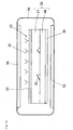
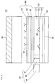
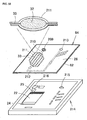
- FIG. 14 shows an exploded sectional view of the structure of a surface plasmon sensor 61 according to an embodiment 2.
- a metal layer 23 is not provided directly on the upper surface of a light guide reflection plate 22, but formed on the upper surface of a relatively thin transparent auxiliary substrate 62, and a surface plasmon resonance layer includes the auxiliary substrate 62 and the metal layer 23.
- the lower surface of the auxiliary substrate 62 is detachably attached to the upper surface of the light guide reflection plate 22 with a matching oil 63 sandwiched between them.
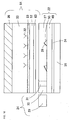
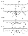
- FIG. 52 shows a sectional view of a variation of the embodiment 13.
- a deflection part 192 is formed by a recession (air layer) having a trapezoidal section in the lower surface of a transparent substrate 48.
- a light emitting unit 24 emits light collimated in the vertical direction only in a fan-like form in a horizontal plane.
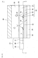
- FIG. 56 shows a sectional view of still another variation of the embodiment 13.
- a plurality of deflection parts 192 having the shape of triangular prism are provided with a transparent resin or cavities having a refractive index smaller than the light guide plate 27 in the surface plasmon sensor shown in FIG. 48 .
- the deflection part 192 is provided in the whole region through which the light passes in this variation also, a light guide reflection plate 22 is prevented from becoming thick by dividing the deflection part 192.
- a light emitting unit 24 emits radiating light in the plane perpendicular to a metal layer 23, it emits hardly spreading light in the plane parallel to the metal layer 23.
Landscapes
- Engineering & Computer Science (AREA)
- General Physics & Mathematics (AREA)
- Physics & Mathematics (AREA)
- Immunology (AREA)
- Health & Medical Sciences (AREA)
- Biochemistry (AREA)
- General Health & Medical Sciences (AREA)
- Chemical & Material Sciences (AREA)
- Life Sciences & Earth Sciences (AREA)
- Pathology (AREA)
- Analytical Chemistry (AREA)
- Human Computer Interaction (AREA)
- Multimedia (AREA)
- Theoretical Computer Science (AREA)
- Investigating Or Analysing Materials By Optical Means (AREA)
- Measurement Of The Respiration, Hearing Ability, Form, And Blood Characteristics Of Living Organisms (AREA)
- Optical Measuring Cells (AREA)
Description
- The present invention relates to an optical component, an optical sensor, a surface plasmon sensor and more particularly, to a surface plasmon sensor for measurement and for fingerprint matching, and an optical component and an optical sensor, etc., used in the above surface plasmon sensor.
- A surface plasmon sensor using a surface plasmon resonance (SPR) has been well known as a sensor that can measure a small amount of antigen , etc with high accuracy in a nondestructive manner. Especially, as human DNA sequence has been completed, a study for using its development has been advancing. Thus, there is a need for a biosensor that can detect protein, DNA, the reaction between an antigen and an antibody at high speed and sensitivity, and thus the surface plasmon sensor has also been used as a biosensor.
- Surface plasmon sensors are described, for example, in
US-A1-2004/090631 ,EP-A2-0 797 090 ,EP-A2-0 965 835 ,WO-A-00/46589 US-A1-2005/179901 ,US 5 822 073 ,EP-A1-0 341 927 , andUS-A1-2005/018194 .US-A1-2004/090631 discloses a surface plasmon resonance sensor having a surface plasmon layer, a light guide reflection plate, and a light source.FIG. 1 shows a sectional view of the structure of a surface plasmon sensor disclosed in Japanese Patent Application Laid-Open No.10-038800 optical housing 12 is detachably put on atransparent substrate housing 11. Thesubstrate housing 11 is provided with alight source unit 13 and a plurality ofphotoelectric detectors 14 arranged in a row. Theoptical housing 12 has a pentagonal or trapezoidal sectional configuration when viewed from the side thereof Aflat mirror 15 and a surfaceplasmon resonance layer 16 comprising an Au thin film, etc is provided on adjacent surfaces of the outer surfaces of theoptical housing 12.Reference numeral 17 designates a spectrum filter. - Thus, according to the surface plasmon sensor, divergent light (polarized light) emitted from the
light source unit 13 upward is reflected by theflat mirror 15 and falls onto the surfaceplasmon resonance layer 16; and the light reflected by the surfaceplasmon resonance layer 16 passes through thespectrum filter 17 and is received by thephotoelectric detector 14. Here, since the divergent light falls on the surfaceplasmon resonance layer 16, eachphotoelectric detector 14 detects the intensity of the light inputted to the surfaceplasmon resonance layer 16 at different incident angles. - This surface plasmon sensor can be used as the biosensor as follows. On the condition that an antibody is fixed to the surface of the surface
plasmon resonance layer 16, when an inspection sample solution containing an antigen that is specifically coupled to the antibody on the surfaceplasmon resonance layer 16 comes in contact with the antibody, the antigen is coupled to the antibody on the surfaceplasmon resonance layer 16. As a result, the refractive index at the interface of the surfaceplasmon resonance layer 16 varies and the intensity of the light received by thephotoelectric detector 14 varies. Thus, when the variation of the light intensity is analyzed, it can be detected whether or not the inspection sample solution contains the antigen that is specifically coupled to the antibody on the surfaceplasmon resonance layer 16, or the density of the antigen can be measured. - Several embodiments of the invention include a small or thin and high accuracy surface plasmon sensor and fingerprint recognition device, and an optical sensor, etc used in the surface plasmon sensor.
- In accordance with one aspect of the present invention, a surface plasmon sensor comprises a light guide reflection plate for guiding light for measurement comprising a plurality of projections disposed on a first surface and a plurality of first reflection surfaces inclined with respect to the first surface and disposed on the plurality of projections, the plurality of projections being positioned so as not to overlap with each other in the emitting direction of the light on a horizontal plane of the first surface, a surface plasmon resonance layer responsive to an object to be measured, positioned on the first surface and comprising a metal layer which is substantially parallel to the first surface of the light guide reflection plate, a light source for emitting the light to said light guide reflection plate, the light source being disposed on an end surface located at an end part of the light guide reflection plate, and a light receiving element disposed on a second surface of the light guide reflection plate opposite the first surface. The light guide reflection plate is transparent to light emitted by the light source. The first reflection surfaces are configured to reflect the light emitted from the light source toward the surface plasmon resonance layer. The metal layer is configured to reflect the light reflected by the first reflection surfaces. The light guide reflection plate is transparent to the light reflected by the metal layer and is configured to emit the light out of the second surface to the light receiving element. The light receiving element is configured to receive the light reflected by the metal layer.
- In accordance with one aspect of the present invention, a flow-type analyzer comprises a surface plasmon sensor as defined in claim 1. The flow-type analyzer further comprises a flow path formed on a surface of the surface plasmon resonance layer opposite to the light guide reflection plate, and a sample supply path and a pump for flowing an inspection sample solutions to the flow path.
- In addition, the components described above can be combined arbitrarily as much as possible.
- Further advantageous embodiments are described in the dependent claims as appended in the claims section.
-
-
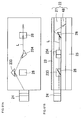
FIG. 1 shows a sectional view of the structure of a conventional surface plasmon sensor; -
FIG. 2 shows an exploded perspective view of a surface plasmon sensor according to an embodiment 1 of the present invention; -
FIG. 3 shows a sectional view of the structure of the surface plasmon sensor according to the embodiment 1 of the present invention; -
FIG. 4 shows a sectional view taken along an X-X line ofFIG. 3 ; -
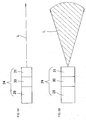
FIG. 5A shows a view of light emitted from a light emitting unit in the embodiment 1 when viewed from a side direction, andFIG. 5B shows a view of the light emitted from the light emitting unit in the embodiment 1 when viewed from above; -
FIG. 6A shows a view of light emitted from another light emitting unit in the embodiment 1 when viewed from a side direction, andFIG. 6B shows a view of the light emitted from another light emitting unit in the embodiment 1 when viewed from above; -
FIG. 7 shows a view of the relation between an inclined angle α of a reflection surface and an incident angle θ of light inputted to a metal layer; -
FIG. 8 shows a view to explain the measurement principle of a general surface plasmon sensor; -
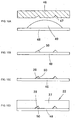
FIGs. 9A to 9D show process charts for explaining exemplary manufacturing steps of a stamper for mass production by 2P (Photo-Polymerization) method; -
FIGs. 10A to 10D show process charts for explaining exemplary mass-producing steps of a light guide reflection plate using the stamper manufactured by the steps shown inFIG. 9 ; -
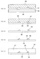
FIGs. 11A to 11E show process charts showing exemplary manufacturing steps of a light guide reflection plate according to several embodiments using an embossing method; -
FIG. 12 shows a sectional view of a possible replacement component of the surface plasmon sensor in the embodiment 1 sealed in a moisture proof case; -
FIG. 13 shows a sectional view of another possible replacement component of the surface plasmon sensor in the embodiment 1 sealed in a moisture proof case; -
FIG. 14 shows an exploded sectional view of the structure of a surface plasmon sensor according to an embodiment 2 of the present invention; -
FIG. 15 shows a sectional view of a replacement component of the surface plasmon sensor of the embodiment 2 sealed in a moisture proof case; -
FIG. 16 shows a partially exploded sectional view of a variation of the embodiment 2; -
FIG. 17 shows a sectional view of a possible replacement component of the variation of the embodiment 2 sealed in a moisture proof case; -
FIG. 18 shows a sectional view of a surface plasmon sensor according to an embodiment 3 of the present invention; -
FIG. 19 shows a sectional view taken along a Y-Y line ofFIG. 18 ; -
FIG. 20 shows a sectional view of a possible variation of the embodiment 3, corresponding to a sectional view taken along the Y-Y line ofFIG. 18 ; -
FIG. 21 shows a sectional view of another possible variation of the embodiment 3; -
FIG. 22 shows a sectional view taken along a Z-Z line ofFIG. 21 ; -
FIG. 23 shows a sectional view of yet another possible variation of the embodiment 3, corresponding to the sectional view taken along the Z-Z line ofFIG. 21 ; -
FIG. 24 shows a sectional view of yet another possible variation of the embodiment 3; -
FIG. 25 shows a sectional view taken along a V-V line ofFIG. 24 ; -
FIG. 26 shows a sectional view of yet another possible variation of the embodiment 3, corresponding to the sectional view taken along the V-V line ofFIG. 24 ; -
FIG. 27 shows a sectional view of the structure of a surface plasmon sensor according to an embodiment 4 of the present invention; -
FIG. 28 shows a sectional view of the structure of a surface plasmon sensor according to an embodiment 5 of the present invention; -
FIG. 29A shows a view of light emitted from a light emitting unit in the embodiment 5 when viewed from a side direction, andFIG. 29B shows a view of the light emitted from the light emitting unit in the embodiment 5 when viewed from above; -
FIG. 30A shows a view of light emitted from another light emitting unit in the embodiment 5 when viewed from a side direction, andFIG. 30B shows a view of the light emitted from another light emitting unit in the embodiment 5 when viewed from above; -
FIG. 31 shows a sectional view of the structure of a surface plasmon sensor according to a possible variation of the embodiment 5; -
FIG. 32 shows a sectional view of the structure of a surface plasmon sensor according to an embodiment 6; -
FIG. 33 shows a schematic view of a reflection point A in a reflection surface, a reflection point B in a metal layer and an incident point C on a light receiving element in the case of the embodiment 1; -
FIG. 34 shows a schematic view of a reflection point A in a reflection surface, reflection point B in a metal layer and an incident point C on a light receiving element in the surface plasmon sensor according to an embodiment 7; -
FIG. 35 shows a view of the planar configurations of a reflection surface and a projection and the configurations of both end surfaces to vary the direction of a reflected light; -
FIG. 36 shows a view of other planar configurations of the reflection surface and the projection and configurations of both end surfaces to vary the direction of a reflected light; -
FIG. 37 shows a view of still other planar configurations of the reflection surface and the projection and configurations of both end surfaces to vary the direction of a reflected light; -
FIG. 38 shows a schematic view of a surface plasmon sensor according to an embodiment 8; -
FIG. 39 shows a schematic view of a variation of the embodiment 8; -
FIG. 40 shows a schematic view of a surface plasmon sensor according to an embodiment 09; -
FIG. 41 shows a schematic view of a surface plasmon sensor according to an embodiment 10; -
FIG. 42 shows a sectional view of the structure of a surface plasmon sensor according to anembodiment 11; -
FIG. 43 shows a schematic view of the surface plasmon sensor according to theembodiment 11; -
FIGs. 44A to 44E show process charts showing one example of manufacturing steps of the surface plasmon sensor in theembodiment 11; -
FIG. 45 shows a sectional view of a surface plasmon sensor according to a variation of theembodiment 11; -
FIGs. 46A to 46D show process charts to explain manufacturing steps of the surface plasmon sensor according to the variation of theembodiment 11; -
FIG. 47 shows a schematic perspective view of a surface plasmon sensor according to anembodiment 12; -
FIG. 48 shows a sectional view of a variation of theembodiment 12; -
FIG. 49 shows a sectional view of a surface plasmon sensor according to anembodiment 13; -
FIGs. 50A to 50D show process charts showing manufacturing steps of a stamper according to theembodiment 13; -
FIGs. 51A to 51D show process charts showing manufacturing steps of a light guide reflection plate in theembodiment 13 using the stamper manufacture inFIG. 50 ; -
FIG. 52 shows a sectional view of a variation of theembodiment 13; -
FIG. 53 shows a sectional view of another variation of theembodiment 13; -
FIGs. 54A to 54E show process charts showing manufacturing steps of the surface plasmon sensor according to another variation of theembodiment 13; -
FIGs. 55A to 55D show process charts showing another manufacturing steps of the surface plasmon sensor according to another variation of theembodiment 13; -
FIG. 56 shows a sectional view of still another variation of theembodiment 13; -
FIG. 57 shows a perspective view of a flow-type analyzer according to anembodiment 14; -
FIG. 58 shows an exploded perspective view of the structure of a surface plasmon sensor incorporated in the above flow-type analyzer shown inFIG 57 ; -
FIG. 59 shows a schematic view of the above flow-type analyzer shown inFIG 57 ; -
FIG. 60 shows a schematic view of a fingerprint recognition device according to anembodiment 15; and -
FIGs. 61A and 61B show schematic views showing a method by which light bypasses a reflection surface and reaches a rear reflection surface in the above fingerprint recognition device according toembodiment 15. - As shown in
FIG. 1 in a conventional surface plasmon sensor, the pentagonal or trapezoidaloptical housing 12 is set on thesubstrate housing 11, the external size becomes large and it is difficult to miniaturize it (an actual product has a size of 41.5 mm in length, 13.5 mm in width and 28.3 mm in height). In addition, according to the above surface plasmon sensor, since the surfaceplasmon resonance layer 16 has a thin strip shape and only one surfaceplasmon resonance layer 16 exists, a plurality of inspections cannot be performed at the same time by fixing the several kinds of the antibodies. If the plurality of inspections are to be performed at the same time, the plurality of surface plasmon resonance layers 16 have to be arranged in the width direction (depth direction of the sheet surface inFIG. 1 ), which further increases the outer size of the surface plasmon sensor. -
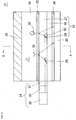
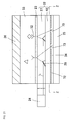
FIG. 2 shows an exploded perspective view of asurface plasmon sensor 21 according to an embodiment 1 of the present invention,FIG. 3 shows a sectional view of the structure of thesurface plasmon sensor 21 according to the embodiment 1, andFIG. 4 shows a sectional view taken along a X-X line ofFIG. 3 . - The
surface plasmon sensor 21 includes a transparent lightguide reflection plate 22 on which a metal layer 23 (surface plasmon resonance layer) is formed, alight emitting unit 24, alight receiving element 25, and achannel cover 26. According to this embodiment, the lightguide reflection plate 22 includes atransparent substrate 48, alight guide plate 27, aprojection 50, and areflection surface 28. Thetransparent substrate 48 includes a transparent glass substrate or a transparent resin substrate and thelight guide plate 27 positioned on thetransparent substrate 48 is formed of a transparent resin such as a polycarbonate resin or a methacrylic resin having the same refractive index as that of thetransparent substrate 48 into the shape of a plate. The plurality ofprojections 50 are sandwiched between thetransparent substrate 48 and thelight guide plate 27, and thereflection surface 28 having a predetermined inclined angle is provided on one inclined surface of theprojection 50 by depositing a metal layer. - Although the plurality of reflection surfaces 28 are positioned in the same horizontal plane, the position of each
reflection surface 28 is not particularly limited. However, it is desirable that light L emitted from thelight emitting unit 24 toward acertain reflection surface 28 is not interrupted by thereflection surface 28 positioned closer to thelight emitting unit 24 than thecertain reflection surface 28. However, even when anotherreflection surface 28 is positioned between thelight emitting unit 24 and thecertain reflection surface 28, since the light emitted toward the direction out of the other reflection surface 28 (the direction in which thereflection surface 28 does not exist) can be guided to thecertain reflection surface 28 by being reflected by a light guiding reflection surface (refer toFIG. 61 ), it is not always that the reflection surfaces 28 must not be overlapped as viewed from thelight emitting unit 24. Particularly, as the density of the reflection surfaces 28 becomes high, since the reflection surfaces 28 are likely to be overlapped, the method using the light guiding reflection surface is effective. - The
light emitting unit 24 is arranged so as to be opposed to the end surface of the lightguide reflection plate 22. Thelight emitting unit 24 includes alight source 29 such as a light emitting diode (LED) or a laser device (LD), apolarizing element 30, and acollimator 31. Thepolarizing element 30 polarizes the light L emitted from thelight source 29 and only passes linearly polarized light in which its polarizing surface is parallel or vertical to the upper surface of the lightguide reflection plate 22. This is because a variation in measurement is to be reduced by using the linearly polarized light in measurement since the reflectance characteristics are different depending on the polarizing direction. In addition, thecollimator 31 is provided for collimating and narrowing a light flux in the direction perpendicular to the upper surface of the lightguide reflection plate 22. While the light L emitted from thelight emitting unit 24 is finely narrowed and collimated light as shown inFIG. 5A when viewed from the side direction of the lightguide reflection plate 22, it spreads out in a fan-like form as shown inFIG. 5B when viewed from the direction perpendicular to the upper surface of the lightguide reflection plate 22. As thecollimator 31 in this case, a slit long in the horizontal direction may be used. Alternatively, it may be such that after the light L from thelight source 29 has been made to be point-like light by passing through a pin hole having a size so as not to diffract, the light is narrowed and collimated by a collimating lens and spreads in the fan-like form in a horizontal plane by for example, a cylindrical lens. - Furthermore, according to another
light emitting unit 24, while the emitted light L is finely narrowed and collimated light as shown inFIG. 6A when viewed from the side direction of the lightguide reflection plate 22, it is emitted toward eachreflection surface 28 discretely as shown inFIG. 6B when viewed from the direction perpendicular to the upper surface of the lightguide reflection plate 22. In this case, thelight source 29 emits pulses of light and after the light L emitted from thelight source 29 has been made to be finely narrowed and collimated light, it is scanned in the horizontal direction with, for example, a small scanner. - The above-described
light emitting unit 24 is set such that its light emitting position may be at the same level as that of thereflection surface 28, so that the light L emitted from thelight emitting unit 24 enters thereflection surface 28 in the horizontal direction. - The
metal layer 23 is formed of Au, Ag, Cu , etc on the whole upper surface of the lightguide reflection plate 22 by vacuum deposition or sputtering. Anantibody 32 is fixed to the upper surface of themetal layer 23 in accordance with an inspection purpose as an element for recognizing a specific molecule and coupling it specifically (referred to as the molecule recognition substance hereinafter). Theantibody 32 is fixed in a region including a position in which the light L reflected from thereflection surface 28 enters themetal layer 23. - The
channel cover 26 having a tunnel-shaped recessed lower surface is bonded to the upper surface of themetal layer 23. Theantibody 32 is covered with thechannel cover 26, and achannel 33 is formed between thechannel cover 26 and themetal layer 23 to pass an inspection sample solution such as blood or body fluid. - The
light receiving element 25 is a two-dimensional light receiving element such as a CCD on which a plurality of small light receivingcells 25a are arranged, and it is detachably adhered to the lower surface of the lightguide reflection plate 22 with a matchingoil 34 for enhancing the optical adherence thereof to prevent the reflection of the light L, sandwiched between them. In addition, the lightguide reflection plate 22 and thelight receiving element 25 are positioned to each other by positioning means using coupling of a projection and a hole and the like. - In this
surface plasmon sensor 21, an inspection can be executed as will be described below. As shown inFIG. 3 , when the light L (polarized light) is emitted from thelight emitting unit 24, the light L collimated in the vertical direction proceeds to in the horizontal direction, spreading in the lightguide reflection plate 22 in the horizontal direction. After the light L has reached thereflection surface 28 and been regularly reflected by thereflection surface 28, it reaches themetal layer 23. Here, when it is assumed that an inclined angle of thereflection surface 28 is α, as shown inFIG. 7 , the light L reflected from thereflection surface 28 enters themetal layer 23 at an incident angle of θ (= 90° - 2α) with respect to a perpendicular line to themetal layer 23. The light L incident themetal layer 23 is totally reflected by the interface between themetal layer 23 and thelight guide plate 27 and then received by thelight receiving cell 25a at a predetermined region in thelight emitting element 25 through thelight guide plate 27 and the matchingoil 34. Since the upper surface and the lower surface of the lightguide reflection plate 22 are parallel and the light L is totally reflected by the upper surface of the lightguide reflection plate 22, when the lower surface of the lightguide reflection plate 22 is in contact with air, it could be totally reflected by the lower surface of the lightguide reflection plate 22. Thus, the matchingoil 34 having a refractive index smaller than those of thetransparent substrate 48 and thelight guide plate 27 is applied to the lower surface of the lightguide reflection plate 22 so that the light L is easily emitted from the lower surface of the lightguide reflection plate 22. - Thus, when the change in light amount in the
light receiving cell 25a is detected, a physical change in a light receiving point of themetal layer 23 is measured. In addition, when the light L reaching the peripheral surface of the lightguide reflection plate 22 is reflected by the peripheral surface of the lightguide reflection plate 22, since this could become noise light or stray light and be detected at thelight receiving element 25 a light absorbing member such as a black plate may be applied to the peripheral surface of the lightguide reflection plate 22. -
FIG. 8 shows a view for explaining the measurement principle of a general surface plasmon sensor (biosensor). The broken line inFIG. 8 indicates the relationship between the incident angle and the reflectance of the light L on the metal layer when the antibody and an antigen are not coupled (before reaction), and the solid line therein designates the relation between the incident angle and the reflectance when the antigen is coupled to the antibody (after reaction). The horizontal axis ofFIG. 8 indicates the incident angle θ of the light L to the metal layer on which the antibody is fixed, and the vertical axis thereof indicates a reflectance R of the light L reflected by the metal layer. - When an antigen that will specifically couple to the antibody on the metal layer is contained in the inspection sample solution, the antigen is coupled to the antibody and captured in the region in which evanescent light exists. As a result, the refractive index at the interface of the metal layer varies and the reflectance characteristics of the light L is shifted to the right as shown by the characteristic curve of the solid line in
FIG. 8 after the reaction, and as the amount of the specifically coupled antigen is increased, the amount of shift to the right increases. Therefore, when the incident angle of the light L to the metal layer is fixed and the variation in the reflectance before and after the antigen is coupled is measured, it can be determined whether or not there is an antigen that was specifically coupled to the antibody and the amount of the antigen that was specifically coupled can be measured. According to such principle, it is well known that even a minute amount of antigen can be detected. Furthermore, by observing the variation in the reflectance continuously in terms of time, the temporal variation in the amount of antigen specifically coupled can be found. - Thus, according to the
surface plasmon sensor 21 in the embodiment 1, when the inspection sample solution containing blood or body fluid is supplied to thechannel 33 and the change in the light amount received in the predeterminedlight receiving cell 25a in thelight receiving element 25 is detected, it can be determined whether or not the antigen that was specifically coupled to theantibody 32 exists in the inspection sample solution, the amount of antigen specifically coupled can be measured, and the temporal variation of that amount can be observed. - Furthermore, according to the
surface plasmon sensor 21, the inclined angle of thereflection surface 28 and the kinds of theantibody 32 fixed to themetal layer 23 may be combined whereby various kinds of inspection methods can be implemented. For example, when a plurality of kinds of reflection surfaces 28 having different inclined angles α are provided in the lightguide reflection plate 22 and the same antigen is fixed to a position in which the light L reflected by thereflection surface 28 is incident, the amount of light received at the plurality of incident angles can be measured at the same time, so that measurement precision can be improved. - In addition, by combining the reflection surfaces 28 having the different inclined angles and the
same antibody 32, it can be easily detected whether there is the reaction between the antigen and the antibody. This reason will be described with reference toFIG. 8 . Two kinds of reflection surfaces having different inclined angles are provided so that the light L is inputted, to themetal layer 23 at the incident angles θa and θb sandwiching the minimum value of the characteristic curve before the reaction, and the reflectance of the light L inputted at the incident angle of θa is set smaller than that of the light inputted at the incident angle of θb before the reaction. Since the reflectance of the light L inputted to themetal layer 23 at the incident angle of θa is increased by ΔRa after the reaction, and the reflectance of the light L inputted to themetal layer 23 at the incident angle of θb is decreased by ΔRb after the reaction, after the reaction has been progressed to some extent, the reflectance of the light L inputted at the incident angle of θa becomes higher than the reflectance of the light L inputted to the metal layer at the incident angle of θb. While the amount of the light L at the incident angle of θa received at thelight receiving cell 25a is smaller than the amount of the light L at the incident angle of θb received at thelight receiving cell 25a in thelight receiving element 25 before the reaction, the amount of the light L at the incident angle of θa received at thelight receiving cell 25a is larger than the amount of the light L at the incident angle of θb received at thelight receiving cell 25a in thelight receiving element 25 after the reaction. Thus, the fact that the reaction between the antigen and the antibody is generated can be easily detected when the both light receiving amounts are inverted. In addition, by branching and leading a part of the light L inputted to thelight receiving element 25 to the outside, when the reaction between the antigen and the antibody is produced, since the brightness of the two signals (reflected light) are inverted, the reaction can be easily observed visually. - Furthermore, when the plurality of reflection surfaces 28 having the same inclined angle of α are arranged along the direction in which the inspection sample solution flows in the
channel 33, and the same kind ofantibodies 32 are fixed to theentire metal layer 23, the behavior (temporal variation) of the antigen in which for example the antigen is specifically coupled to theantibody 32 and separated from theantibody 32 and then coupled to theantibody 32 downstream can be observed. - In addition, when the plurality of reflection surfaces 28 having the same inclined angle of α are provided in the light
guide reflection plate 22, anddifferent antibodies 32 are fixed to different positions on themetal layer 23 to which the light L reflected by the reflection surfaces 28 are incident, the plurality of kinds of antigens that are specifically coupled to theantibodies 32 can be inspected at the same time, so that the inspection operation can be more efficiently carried out. - Furthermore, when a plurality of reflection surfaces 28 having the same inclined angle of α are provided in the light
guide reflection plate 22, the same kind ofantibodies 32 are fixed to theentire metal layer 23, and thechannel 33 is divided so that different inspection sample solutions flow in the divided areas, a plurality of kinds of the antigens that are specifically coupled to the antibodies can be inspected at the same time, so that the inspection operation can be more efficiently carried out. - In addition, any of the above-mentioned inspection methods may be combined.
- According to the above
surface plasmon sensor 21, since the plate-shaped lightguide reflection plate 22 and light receivingelement 25 are used, thesurface plasmon sensor 21 can be miniaturized and thinned. Especially, even when the number of reflection surfaces 28 is increased and the inspections are performed at the plurality of positions; its external size is substantially the same. In addition, since thereflection surface 28 may have any inclined angle and it may be set at any position, the channel in which the inspection sample solution flows can be designed in a plane, so that the degree of freedom of the fixed positions of the channel and the antibody is increased and a plurality of kinds of antibodies can be fixed or the antibodies can be fixed to the plurality of positions. Thus, thesurface plasmon sensor 21 can be miniaturized and thinned keeping high inspection efficiency and high inspection accuracy. -
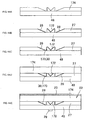
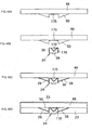
FIGs. 9A to 9D show process charts for explaining exemplary steps for manufacturing the stamper for mass-production by Photo-Polymerization (2P) method, andFIGs. 10A to 10D show process charts for explaining exemplary steps for mass-producing a lightguide reflection plate 22 using the stamper. - A
substrate 41 is prepared and an electron beam resist 42 is applied thereon. Then, as shown inFIG. 9A , the resist 42 is microfabricated by applying the electron beam over amask 43, and as shown inFIG. 9B , amodel 44 of theprojection 50 on which thereflection surface 28 is formed is manufactured with the resist 42 on thesubstrate 41. - After a
matrix 45 having themodel 44 of theprojection 50 has been manufactured, as shown inFIG. 9C , a stamper material such as nickel is deposited on thematrix 45 by an electroforming method, whereby thestamper 46 is manufactured. Then, as shown inFIG. 9D , thestamper 46 is removed from thematrix 45, and thestamper 46 is completed. According to thestamper 46, a recessedpart 47 is formed corresponding to the configuration of themodel 44 of theprojection 50. - After the
stamper 46 has been manufactured, the lightguide reflection plate 22 is mass-produced using thestamper 46 by the 2P method. First, as shown inFIG. 10A , after a UV curedresin 49 has been dropped on atransparent substrate 48 which may be for example a transparent glass substrate or a transparent resin substrate, thestamper 46 is lowered onto the UV curedresin 49 so that the UV curedresin 49 is sandwiched between thetransparent substrate 48 and thestamper 46 and the recessedpart 47 of thestamper 46 is filled with the UV curedresin 49. - Then, the UV cured
resin 49 is irradiated with UV light from the side of thetransparent substrate 48. Thus, the UV curedresin 49 is cured by a light curing reaction. After the UV curedresin 49 has been cured, thestamper 46 is removed from the UV curedresin 49, whereby thetriangular projection 50 including the UV curedresin 49 is formed on thetransparent substrate 48 as shown inFIG. 10B . - One inclined surface of the
projection 50 has a predetermined inclined angle and a metal thin film formed of Ag, Al, Cu , etc is selectively deposited on the inclined surface, whereby thereflection surface 28 is formed on the inclined surface of theprojection 50 as shown inFIG. 10C . The method of selectively depositing the metal thin film includes a lift-off method in which the metal thin film is deposited from above a resist having an opening at one part by sputtering and unnecessary metal thin film is removed together with the resist, a micro-molding method, a screen printing method, and an ink-jetting method. Then, thelight guide plate 27 is formed of a resin having the same refractive index as that of thetransparent substrate 48 on thetransparent substrate 48, to complete the lightguide reflection plate 22 in which theprojection 50 and thereflection surface 28 are buried in thetransparent substrate 48 and thelight guide plate 27. - In addition, according to another method of manufacturing the light
guide reflection plate 22, the lightguide reflection plate 22 may be duplicated using an embossing method.FIGs. 11A to 11E show process charts of step for manufacturing a lightguide reflection plate 22 using the embossing method. According to the steps, as shown inFIG. 11A , after aresin 52 such as an acrylic resin has been spin-coated on thetransparent substrate 48, thestamper 46 manufactured by the steps shown inFIG. 9 is put on thetransparent substrate 48, and theresin 52 is pressed by thestamper 46 as shown inFIG. 11B . - When the
stamper 46 is removed, as shown inFIG. 11C , the same pattern as themodel 44 of theprojection 50 is transferred on thetransparent substrate 48, whereby theprojection 50 is formed. Then, as shown inFIG. 11D , thereflection surface 28 is formed on the inclined surface of theprojection 50 and as shown inFIG. 11E , thelight guide plate 27 is formed on the upper surface of thetransparent substrate 48 from above theprojection 50 and thereflection surface 28, whereby the lightguide reflection plate 22 is manufactured. - According to the conventional example, although it is not suitable for the mass production because it is manufactured by a batch processing, according to the
surface plasmon sensor 21, since it can be duplicated by a duplicating method using the stamper, they can be mass-produced, so that its manufacturing cost can be low. - Next, a description will be made of a method of reusing the above
surface plasmon sensor 21. In the usedsurface plasmon sensor 21, after the inspection sample solution has passed through thechannel 33, the antigen and a biomolecule are attached on theantibody 32 on themetal layer 23. When it is used in a laboratory, this may be cleaned to remove the antigen and the antibody attached on the metal layer from the metal layer and a desired new antibody can be fixed to the metal layer again. However, in the medical field, the above reuse method is not efficient. - Therefore, it may be desired that the
surface plasmon sensor 21 is to be disposable, that is, it is to be abandoned after use. However, since thelight source 29 and thelight receiving element 25 used in thesurface plasmon sensor 21 are expensive, when the wholesurface plasmon sensor 21 is thrown away after use, the cost of thesurface plasmon sensor 21 becomes high. Thus, according to asurface plasmon sensor 21 according to embodiment 1, may be partially disposable. - According one method, the
light emitting unit 24 and thelight receiving element 25 and thechannel cover 26 are to be repetitively used and the lightguide reflection plate 22 on which themetal layer 23 is formed is to be replaced with areplacement component 53 after each use. Thereplacement component 53 is provided by thinly applying the matchingoil 34 on the lower surface of the lightguide reflection plate 22 on which themetal layer 23 has been formed and theantibody 32 is fixed to themetal layer 23. Thereplacement components 53 in which various kinds of antibodies can be fixed in accordance with the purpose are to be prepared. Although a special technique has been needed to fix the antibody to the metal layer and a specialist has fixed the antibody to the metal layer at the scene it is used conventionally, since theantibody 32 has been fixed to themetal layer 23 in thereplacement component 53 previously, it is not necessary to fix theantibody 32 by a user, so that the replacement component can be used without any special technique. In addition, since the lightguide reflection plate 22 is adhered to thelight receiving element 25 with the matchingoil 34 sandwiched between them, when the matchingoil 34 has been thinly applied to the lower surface of thereplacement component 53, a process for applying the matchingoil 34 can be omitted. - The
replacement component 53 is supplied to the market such that it is sealed in amoisture proof case 54 formed of a moisture proof film or plastic as shown inFIG. 12 . Since theantibody 32 and the matchingoil 34 could be dried and especially theantibody 32 has to be moist constantly, thereplacement component 53 is sealed in themoisture proof case 54 so that theantibody 32 and the matchingoil 34 are prevented from being dried. In addition,sponges moisture proof case 54, and thereplacement component 53 is set such that the surface on which the matchingoil 34 is applied is put on thesponge 55 on the bottom. Thesponge 55 contains the matching oil, so that the matchingoil 34 of thereplacement component 53 is prevented from being dried and the matchingoil 34 of thereplacement component 53 is prevented from being absorbed by thesponge 55. Thesponge 56 on the top surface contains water, so that theantibody 32 fixed to themetal layer 23 is prevented from being dried and kept in the moist state. - Thus, in using the
replacement component 53, it is taken out of themoisture proof case 54 and put on thelight receiving element 25 and adhered onto the upper surface of thelight receiving element 25 through the matchingoil 34. In addition, thechannel cover 26 is bonded to themetal layer 23, and thelight emitting unit 24 is positioned and mounted on the end surface of the lightguide reflection plate 22, to inspect the antigen, etc. - After the inspection has been completed, the
channel cover 26, thelight emitting unit 24 and thelight receiving element 25 are removed from thereplacement component 53 and thereplacement component 53 is put back in themoisture proof case 54 and abandoned. - Thus, since the
replacement component 53 is disposable, thesurface plasmon sensor 21 can be easily used without any specialist, and since the expensivelight emitting unit 24 and light receivingelement 25 can be repetitively used, the cost of thesurface plasmon sensor 21 can be lowered. - In addition, as shown in
FIG. 13 , thereplacement component 53 may include thechannel cover 26. In this case, thechannel cover 26 is integrally bonded to the upper surface of themetal layer 23, so that the lightguide reflection plate 22 is sealed in themoisture proof case 54 with thechannel cover 26 attached. In this case, since theantibody 32 is positioned in thechannel 33, when an appropriate moisturizing agent such as a buffer is put in thechannel 33 and both ends of thechannel 33 are blocked withstoppers 57 which may be for example a rubber or flexible plastic as shown inFIG. 13 , theantibody 32 is prevented from drying out. At the time of use, thereplacement component 53 is taken out of themoisture proof case 54 and thestoppers 57 on both ends are removed. In this case, since theantibody 32 is not dried, it is not necessary to prepare thesponge 56 containing water (thesponge 55 containing the matching oil may be eliminated), thereplacement component 53 can be stored in a case having no moisture proofing, so that its handling can be simplified. - In addition, in the case where the light
guide reflection plate 22 is exchanged as thereplacement component 53, although in the very least, thelight receiving cell 25a in thelight receiving element 25 may be provided at the position to which the light L reflected by themetal layer 23 is incident, since the position of thereflection surface 28 could be changed with respect to eachreplacement component 53, the light receivingcells 25a may be provided on the wholelight receiving element 25. - In addition, although the reaction between the antibody and the antigen is used in the embodiment 1, the surface plasmon sensor (biosensor) according to several embodiments of the present invention may be used when various kinds of proteins and DNA are fixed to the substrate and couplings between the proteins and between the DNA and protein are used. In addition, when an appropriate material is selected as the molecule recognition substance is fixed onto the metal layer, the biosensor can be used in measuring an organic or inorganic matter instead of the biological material (the same is true of the following embodiments).
-
FIG. 14 shows an exploded sectional view of the structure of asurface plasmon sensor 61 according to an embodiment 2. According to embodiment 2, ametal layer 23 is not provided directly on the upper surface of a lightguide reflection plate 22, but formed on the upper surface of a relatively thin transparentauxiliary substrate 62, and a surface plasmon resonance layer includes theauxiliary substrate 62 and themetal layer 23. In the surface plasmon resonance layer according to this embodiment, the lower surface of theauxiliary substrate 62 is detachably attached to the upper surface of the lightguide reflection plate 22 with a matchingoil 63 sandwiched between them. Theauxiliary substrate 62 includes a transparent glass substrate, a transparent resin plate, a transparent resin film , etc, and it may have the same refractive index as that of alight guide plate 27 of the lightguide reflection plate 22. Although it is not shown, positioning means including a recession and α projection , etc is provided between the lightguide reflection plate 22 and theauxiliary substrate 62. In addition, according to thesurface plasmon sensor 61 of the embodiment 2, apolarizing element 30 and acollimator 31 that constitute a part of alight emitting unit 24 are incorporated in the lightguide reflection plate 22 and alight source 29 is arranged opposite thepolarizing element 30 buried in the lightguide reflection plate 22. - According to this
surface plasmon sensor 61, areplacement component 64 is provided such that anantibody 32 is fixed onto themetal layer 23 formed on the upper surface of theauxiliary substrate 62 and the matchingoil 63 is thinly applied to the lower surface of theauxiliary substrate 62. Thisreplacement component 64 is kept in amoisture proof case 54 as shown inFIG. 15 . - According to the embodiment 2, since the light
guide reflection plate 22 can be also repeatedly reused, the reusability of thesurface plasmon sensor 61 is more improved as compared with the embodiment 1. In addition, since theauxiliary substrate 62 can be manufactured at lower cost than the lightguide reflection plate 22 incorporating areflection surface 28, thereplacement component 64 can be provided at lower cost than that of the embodiment 1. - In addition, the
reflection surface 28 may be formed by forming a triangular recession on the lower surface of the lightguide reflection plate 22 and forming a metal layer on the surface of the recession. That is, thereflection surface 28 may be formed in the recession provided in the lower surface of thelight guide plate 27 and the lower surface of thelight guide plate 27 becomes the lower surface of the lightguide reflection plate 22 without providing atransparent substrate 48. However, in the case where the lightguide reflection plate 22 is reused like in the embodiment 2, when thereflection surface 28 is sealed in the lightguide reflection plate 22, thereflection surface 28 is not likely to be removed or damaged, so that high durability can be provided. - In addition, whether the
polarizing element 30 and thecollimator 31 are contained in the replacement component or not is determined in view of its measurement precision and cost. When thepolarizing element 30 and thecollimator 31 are contained in the replacement component, although it is not necessary to adjust positions between that optical system and thereflection surface 28, the number of manufacturing steps of the replacement component is increased and its manufacturing cost is also increased. Meanwhile, when they are not contained in the replacement component, although the manufacturing steps of the replacement component can be simplified and its manufacturing cost is reduced, optical adjustment could be necessary between the replacement component and thelight emitting unit 24. -
FIG. 16 shows a sectional view of a variation of the embodiment 2. According to this variation, achannel cover 26 is integrally bonded onto ametal layer 23 of anauxiliary substrate 62 and areplacement component 64 includes theauxiliary substrate 62 for forming ametal layer 23, anantibody 32, a matchingoil 63 and thechannel cover 26. Then, as shown inFIG. 17 , an appropriate moisturizing agent such as a buffer is put in achannel 33 formed between theauxiliary substrate 62 and thechannel cover 26, both ends of thechannel 33 are blocked withstoppers 57, and thereplacement component 64 is kept in amoisture proof case 54. -
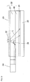
FIG. 18 shows a sectional view of asurface plasmon sensor 71 according to an embodiment 3, andFIG. 19 shows a sectional view of a section (taken along a Y-Y line ofFIG. 18 ) in a horizontal plane areflection surface 28 is arranged. According to thesurface plasmon sensor 71 of the embodiment 3, alight shielding part 72 impenetrable to light L is provided almost entirely between the upper surface of atransparent substrate 48 and the lower surface of alight guide plate 27 so as to almost correspond to a horizontal plane passing the lower end of areflection surface 28. Atransparent hole 73 is provided at a position through which the light L reflected by thereflection surface 28 and ametal layer 23 passes, in thelight shielding part 72. Thelight shielding part 72 is preferably formed of a light-absorbing material such as a black film. Thelight shielding part 72 may be provided on the upper surface of thetransparent substrate 48 by sputtering at the step shown inFIG. 10B or FIG. 10C . In addition, thetransparent hole 73 is formed in thelight shielding part 72 by partial sputtering when thelight shielding part 72 is formed on thetransparent substrate 48, or thetransparent hole 73 is formed by etching or lift-off method after the whole-surface sputtering. Alight emitting unit 24 emits light collimated in the vertical direction only so as to spread it out in a fan-like form in a horizontal plane. - According to the embodiment 3, since the light L except for the light needed in measurement can be prevented from entering a
light receiving element 25 by thelight shielding part 72, unnecessary light such as noise light and stray light reflecting diffusely in the lightguide reflection plate 22 can be prevented from entering thelight receiving element 25, and only the reflected light having a predetermined angle enters thelight receiving element 25, so that measurement precision can be enhanced. - In addition, since the light L entering a
light receiving cell 25a sufficiently apart from alight receiving cell 25a to which the reflected light having the predetermined angle is inputted does not affect the measurement precision, thelight shielding part 72 may be provided only around thetransparent hole 73 as shown inFIG. 20 . - In addition, the
light shielding part 72 may be positioned on any surface. For example, as shown inFIGs. 21 and22 , thelight shielding part 72 is entirely provided on the lower surface of the lightguide reflection plate 22 except for thetransparent hole 73 to prevent the noise light and the stray light from entering thelight receiving element 25. Thelight shielding part 72 may be formed on the lower surface of the lightguide reflection plate 22 by partial sputtering at the manufacturing steps of the lightguide reflection plate 22. In this case also, thelight shielding part 72 may be provided only around thetransparent hole 73 as shown inFIG. 23 . -
FIG. 24 shows a sectional view of a variation of the embodiment 3, andFIG. 25 shows a sectional view taken along a V-V line inFIG. 24 . According to this variation, a light-absorbinglight shielding part 72 is provided on the upper surface of a lightguide reflection plate 22, and atransparent hole 73 is provided at the position in which light L reflected by areflection surface 28 is reflected by themetal layer 23. According to this variation, since noise light and stray light in the lightguide reflection plate 22 are reflected at the position in themetal layer 23 in which the reflected light from thereflection surface 28 is not inputted and can be prevented from entering thelight receiving cell 25a used in measurement, the measurement precision of the surface plasmon sensor can be improved. Thelight shielding part 72 may be formed on the upper surface of the lightguide reflection plate 22 by partial sputtering at the manufacturing step of the lightguide reflection plate 22. In this case also, thelight shielding part 72 may be provided only around thetransparent hole 73 as shown inFIG. 26 . -
FIG. 27 shows a sectional view of the structure of asurface plasmon sensor 81 according to an embodiment 4 of the present invention. According to the embodiment 4, aspectral element 82 for example a diffraction grating is provided between a position in which light L reflected by areflection surface 28 is inputted to ametal layer 23 and alight receiving element 25. For example, as shown inFIG. 27 , thespectral element 82 is provided on the upper surface of thelight receiving element 25. Thus, a lightguide reflection plate 22 is adhered on thespectral element 82 with a matchingoil 34 sandwiched between them. Alight emitting unit 24 emits white light collimated only in the vertical direction in a fan-like form in a horizontal plane. - Thus, according to the above
surface plasmon sensor 81, the white light is emitted from thelight emitting unit 24 and the light L reflected by thereflection surface 28 is inputted to themetal layer 23 at a constant incident angle. The white light reflected by themetal layer 23 is inputted to thespectral element 82 to be dispersed into spectrum with respect to each wavelength and the light L from thespectral element 82 is inputted to differentlight receiving cells 25a. - Even the light L reflected by the
metal layer 23 has the same incident and reflected angle in themetal layer 23, its variation in light intensity (variation in the light amount received by thelight receiving cell 25a) depends on the wavelength of the light L. For example, when there is no reaction between an antibody and a antigen, a yellow component of the reflected light becomes dark because it is absorbed by plasmon resonance. Meanwhile, when there is the reaction between the antibody and the antigen, a green component of the reflected light becomes dark. In addition, although the variation in the color of the reflected light (light frequency) depends on the kind of the antibody, when the white light is emitted from thelight emitting unit 24 and dispersed into spectrum by thespectral element 82, the measurement can be performed using the light L of a specific and any wavelength, so that measurement light of an optimum wavelength can be selected according to the kind of the antibody. That is, when one white light is reflected by themetal layer 23, the same effect provided when monochromatic light is inputted to themetal layer 23 at a plurality of incident angles can be provided, so that the number of surfaces at the region in which the antibody is fixed and the light L is inputted (referred to as the reflection surface region occasionally) can be reduced. Thus, according to thesurface plasmon sensor 81 of the embodiment 4, since the number of reflection surfaces can be reduced, thesurface plasmon sensor 81 can be further miniaturized. -
FIG. 28 shows a sectional view of the structure of asurface plasmon sensor 91 according to an embodiment 5 of the present invention. According to the surface plasmon sensor, a channel for flowing an inspection sample solution is not always necessary, and an inspection sample solution can be dropped from a pipette to a reflection surface region in which an antibody is fixed, for example. Therefore, in the following embodiment, thechannel cover 26 is omitted except for a case where it has to be shown especially. - A
light emitting unit 24 in the embodiment 5 does not comprise a collimator and includes alight source 29 and apolarizing element 30. Therefore, thelight emitting unit 24 emits light L spreading in the vertical direction also. While the light L emitted from thelight emitting unit 24 slightly spreads when viewed from the side direction of a lightguide reflection plate 22 as shown inFIG. 29A , it largely spreads when viewed from the direction perpendicular to the upper surface of the lightguide reflection plate 22 as shown inFIG. 29B . Alternatively, the light L emitted from thelight emitting unit 24 may slightly spread when viewed from the side direction of the lightguide reflection plate 22 as shown inFIG. 30A , and it may be emitted discretely toward eachreflection surface 28 when viewed from the direction perpendicular to the upper surface of the lightguide reflection plate 22 as shown inFIG. 30B . - According to the embodiment 5, since the light L emitted from the
light emitting unit 24 spreads in the plane perpendicular to the upper surface of the lightguide reflection plate 22, the spreading light L can be inputted to the reflection surface region, that is, the light L whose incident angles vary within a certain range can be inputted to themetal layer 23 by the onereflection surface 28. Therefore, the same effect as that in the case of the plurality of reflection surfaces having different inclined angles can be implemented with the onereflection surface 28 and detection can be implemented by the light L having incident angles that vary sequentially in one reflection surface region. As a result, while the same inspection is performed, the number of the surfaces at the reflection surface region can be reduced and thesurface plasmon sensor 91 can be further miniaturized. -
FIG. 31 shows a variation of the embodiment 5. According to this embodiment 5, similar to thelight emitting unit 24 in the embodiment 1, alight emitting unit 24 emits light collimated in the vertical direction only in a fan-like form in a horizontal plane. Meanwhile, since areflection surface 28 is curved like a convex mirror, similar to the embodiment 5, the radiating light L is inputted to the reflection surface region in which theantibody 32 is fixed. Thus, the same effect as that of the embodiment 5 can be provided in this variation also, and the surface plasmon sensor can be miniaturized. -
FIG. 32 shows a sectional view of the structure of asurface plasmon sensor 101 according to an embodiment 6. According to thesurface plasmon sensor 101, light L slightly spreading in a plane perpendicular to ametal layer 23 is emitted from alight emitting unit 24. Meanwhile, areflection surface 28 is curved like a concave mirror. Thisreflection surface 28 is designed such that after the light emitted from thelight emitting unit 24 has been reflected by thereflection surface 28 and themetal layer 23, it is converged to a specificlight receiving cell 25a. - Thus, according to this embodiment, even when the light L from the
light emitting unit 24 spreads, the variation in incident angle of the light L inputted to themetal layer 23 can be reduced by converging the reflected light on thereflection surface 28, so that measurement precision can be improved. - In addition, the light L inputted to a certain reflection surface region at different incident angles and reflected there can be received by a specific
light receiving cell 25a, so that the integration value of the intensity of the light L inputted to a certain reflection surface region at different angles and reflected there can be measured. Thus, in this embodiment also, while the same inspection is performed, the number of the surfaces at the reflection surface region can be reduced and thesurface plasmon sensor 91 can be further miniaturized. -
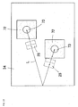
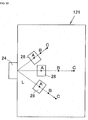
FIG. 33 shows a schematic view of an inputted and reflected point A in thereflection surface 28, an inputted and reflected point B in themetal layer 23, and an inputted point C to thelight receiving element 25 in the case of the embodiment 1. Since the light L emitted from thelight emitting unit 24 radiates and the light L goes straight before and after reflected by thereflection surface 28 when viewed from the direction perpendicular to the upper surface of the lightguide reflection plate 22, the area of thesurface plasmon sensor 21 in the structure according to the embodiment 1 becomes large, so that miniaturization is limited. - Thus, according to a
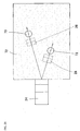
surface plasmon sensor 121 of an embodiment 7, a method for further miniaturizing it is proposed.FIG. 34 shows a schematic view of an inputted and reflected point A in areflection surface 28, an inputted and reflected point B in ametal layer 23, and an inputted point C to alight receiving element 25 in thesurface plasmon sensor 121 of the embodiment 7. According to thesurface plasmon sensor 121 of the embodiment 7, the direction of the light L reflected by thereflection surface 28 is bent so that the reflected point in themetal layer 23 and the inputted point to alight receiving element 25 are converged to the center point when viewed from the direction perpendicular to the upper surface of a lightguide reflection plate 22. - Thus, according to the above
surface plasmon sensor 121, thesurface plasmon sensor 121 is further miniaturized by narrowing the width of thesurface plasmon sensor 121. - In order to change the direction of the light L reflected by the
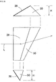
reflection surface 28, the direction of thereflection surface 28 is to be changed.FIG. 35 shows the planar configurations of thereflection surface 28 and theprojection 50 and configurations of the end surfaces on both sides. Although the height H of thereflection surface 28 is constant, the inclined angle of thereflection surface 28 varies along the width direction of thereflection surface 28 inFIG. 35 . Therefore, as shown inFIG. 35 , the light L reflected by thereflection surface 28 is bent in plane view also. According to such structure, since the inclined angle of thereflection surface 28 varies along the width direction of thereflection surface 28, the light L can be reflected at different inclined angles by the onereflection surface 28, so that thesurface plasmon sensor 121 can be miniaturized. -
FIG. 36 shows the planar configurations of thereflection surface 28 and theprojection 50 and configurations of the end surfaces on both sides. Although the vertical sectional configuration of anyprojection 50 is an isosceles triangle, the heights of thereflection surface 28 and theprojection 50 vary along the width direction of thereflection surface 28, that is, the height at one end surface is H1 and the height at the other end surface is H2 (>H1) inFIG. 36 . Therefore, as shown inFIG. 36 , the light L reflected by thereflection surface 28 is bent in plane view also. According to such structure also, since the inclined angle of thereflection surface 28 varies along the width direction of thereflection surface 28, the light L can be reflected at different inclined angles by the onereflection surface 28, so that thesurface plasmon sensor 121 can be miniaturized. - Furthermore, as shown in
FIG. 37 , even when the light emitted from thelight emitting unit 24 is diffused, the direction of the light L reflected by thereflection surface 28 can be bent and the reflected light can be converged by bending thereflection surface 28 and theprojection 50. -
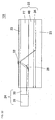
FIG. 38 shows a schematic view of asurface plasmon sensor 141 according to an embodiment 8 of the present invention. According to thesurface plasmon sensor 141, alight emitting unit 24 and eachreflection surface 28 are arranged so that inputted and reflected points B of light L reflected byreflection surfaces 28 may be aligned in a straight line in ametal layer 23. Thus, anarrow channel 33 is formed in achannel cover 26 so that it may pass the inputted and reflected points B of the light L in themetal layer 23. - According to the embodiment 1, since the
channel 33 is formed on the whole upper surface of themetal layer 23, the sectional area of thechannel 33 is large, so that the large amount of the inspection sample solution has to flow in thechannel 33. Furthermore, when the inputted and reflected points B of the light L arranged arbitrarily are to be connected by a narrow channel, the channel could be curved or skewed and become a complicated form, which makes the control of the flow of the inspection sample solution difficult. - Meanwhile, according to the
surface plasmon sensor 141 in the embodiment 8, since the inputted and reflected points B of the light L are aligned, thechannel 33 can be narrowed and the measurement can be implemented by the small amount of the inspection sample solution. In addition, since thechannel 33 for the inspection sample solution can be linear, the flow of the inspection sample solution can be easily controlled. - In addition, as shown in
FIG. 39 , when the plurality ofsurface plasmon sensors 141 are arranged in the same plane, and thechannels 33 of thesurface plasmon sensors 141 are linearly connected, or thosechannels 33 are arranged in parallel and connected to branched channels, thesurface plasmon sensors 141 can be arrayed, so that the same inspection sample solution can be measured using different antibodies in thesurface plasmon sensors 141 at the same time. -
FIG. 40 shows a schematic view of asurface plasmon sensor 151 according to an embodiment 09 of the present invention. According to thesurface plasmon sensor 151, alight emitting unit 24 and areflection surface 28 , etc are arranged such that inputted points C to alight receiving element 25 are aligned in a straight line at almost the same intervals. More specifically, the position and the inclined angle of thereflection surface 28 are adjusted and the direction (direction of the reflection surface 28) of the reflected light from thereflection surface 28 is adjusted so that the inputted points C of the light L to thelight receiving element 25 are aligned and arranged at almost the same intervals. Thus, a one-dimensional photodiode array is provided at each inputted point C as alight receiving cell 25a (photodiode). - According to the
surface plasmon sensor 151, an inexpensive one-dimensional photodiode array such as the photodiode array can be used in thelight receiving element 25 instead of the CCD. - In addition, according to the
surface plasmon sensor 141 shown inFIG. 14 also, since the inputted points C of the light L in thelight receiving element 25 are aligned, the inexpensive one-dimensional light receiving element such as the photodiode array may be used in thelight receiving element 25. In addition, according to thesurface plasmon sensor 151 inFIG. 40 , since the inputted and reflected points B of the light L in themetal layer 23 are not aligned, although the inputted and reflected points B may be connected by a curved narrow channel, the inputted and reflected points B may be connected by alinear channel 33 having a narrow width as much as possible and containing all of the inputted and reflected points B as shown by a phantom line inFIG. 40 . -
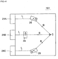
FIG. 41 shows a schematic view of asurface plasmon sensor 161 according to an embodiment 10 of the present invention. According to thesurface plasmon sensor 161, a plurality of light emittingunits guide reflection plate 22. Narrow lights L that are made parallel in a perpendicular plane and a horizontal plane with respect to the upper surface of the lightguide reflection plate 22 are emitted from thelight emitting unit 24. Thus, the position, inclined angle and direction of thereflection surface 28 are adjusted such that light L emitted from eachlight emitting unit 24, reflected by areflection surface 28, and reflected by ametal layer 23 at each reflected angle may be inputted to one inputted point C. At the inputted point C, an inexpensivelight emitting unit 25 such as a photodiode is arranged. - In addition, in order to take different measurement by the light L of each optical path, the reflection surfaces 28 have different inclined angles from each other or different kinds of antibodies are fixed to the inputted and reflected points B of the light L in the
metal layer 23. - Thus, according to the
surface plasmon sensor 161, the light is emitted sequentially from the plurality of light emitting units such that24A 24C, for example and received by the same→ 24B →light emitting unit 25. According to this embodiment, since one element (photodiode, for example) is used for thelight receiving element 25, there are advantages that the cost of thelight receiving element 25 can be inexpensive and since the same element is used, there is no measurement variation or an error in thelight receiving element 25. -
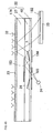
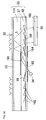
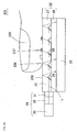
FIG. 42 shows a sectional view of the structure of asurface plasmon sensor 171 according to anembodiment 11 of the present invention, andFIG. 43 shows a schematic view of thesurface plasmon sensor 171. Alight emitting unit 24 of thesurface plasmon sensor 171 includes alight source 29, a cone-shapedreflection plate 172, apolarizing element 30, and a light-absorbinglight shielding plate 173 and arranged in the center of a lightguide reflection plate 22. Thelight source 29 is arranged so as to emit light L (parallel light) upward, and the cone-shaped or polygonal cone-shapedreflection plate 172 having a reflection surface on its lower surface is arranged above thelight source 29. Thepolarizing element 30 is formed in a cylindrical shape or a polygonal cylindrical shape so as to surround the cone-shapedreflection plate 172, and a slit or a small hole extending in the horizontal direction is opened in thelight shielding plate 173 provided on the peripheral surface of thepolarizing element 30. Therefore, when the light L is emitted upward from thelight source 29, the light emitted from thelight source 29 is reflected by the reflection surface of the cone-shapedreflection plate 172 and spreads to the peripheral direction and only straight polarized light in the horizontal direction or the perpendicular direction passes through thepolarizing element 30. Then, when it passes through the slit or hole of thelight shielding plate 173, collimated light that hardly spreads in the perpendicular direction is emitted to the whole direction or the direction in which thereflection surface 28 is arranged in the lightguide reflection plate 22. - The light
guide reflection plate 22 has a structure in which both upper and lower surfaces of alight guide plate 27 in which the plurality of reflection surfaces 28 are formed are sandwiched by an auxiliary substrate 174 (protection layer) and atransparent substrate 48, respectively. Thelight guide plate 27, theauxiliary substrate 174 and thetransparent substrate 48 are all transparent and have the same refractive index. The plurality of reflection surfaces 28 are provided at appropriate positions at almost the same level as the horizontal plane in which the light L is emitted, in the lightguide reflection plate 22. Here, it is to be noted that the reflection surfaces 28 are arranged so as not to overlap with each other in the emitting direction of the light L. - A
metal layer 23 is formed of Au or Ag on the upper surface of the lightguide reflection plate 22, anantibody 32 is fixed to a region to which the light L reflected by thereflection surface 28 is inputted. - In addition, the lower surface of the light
guide reflection plate 22 is closely adhered to the upper surface of thelight receiving element 25 with a matchingoil 34 sandwiched between them. Thelight receiving element 25 includes a two-dimensional light receiving element such as a CCD. - Thus, in the
surface plasmon sensor 171 also, the light emitted from thelight emitting unit 24 and reflected by thereflection surface 28 is reflected by a reflection surface region to which theantibody 32 is fixed and inputted to thelight receiving element 25. Thus, the intensity and variation of the light L is measured. In addition, inFIG. 43 also, reference character A designates an inputted and reflected point of the light L in thereflection surface 28, reference character B designates an inputted and reflected point of the light L in themetal layer 23, and reference character C designates an inputted point of the light L in thelight receiving element 25. - According to the above structure, since the reflection surfaces 28 , etc can be radially arranged centering around the
light emitting unit 24, there is less wasted region in the lightguide reflection plate 22, many reflection surface regions can be set for onelight emitting unit 24, and more reactions between the antibody and antigen can be detected. - A manufacturing method of the
surface plasmon sensor 171 will be described hereinafter.FIGs. 44A to 44E show process charts showing one example of the manufacturing steps of thesurface plasmon sensor 171. First, a UV cured resin is supplied to thetransparent substrate 48, and this is pressed by a stamper (not shown) and cured. Thus, as shown inFIG. 44A , thelight guide plate 27 having a pattern surface for forming the cone-shapedreflection plate 172 and thereflection surface 28 is formed. - Then, as shown in
FIG. 44B , a metal layer film is deposited on the pattern surface for forming the cone-shapedreflection plate 172 and thereflection surface 28 on the surface of thelight guide plate 27 to form the cone-shapedreflection plate 172 and thereflection surface 28. - Then, as shown in
FIG. 44C , the cylindrical or polygonalpolarizing element 30 and thelight shielding plate 173 are provided in the periphery of the cone-shapedreflection plate 172 and then as shown inFIG. 44D , theauxiliary substrate 174 is laminated on thelight guide plate 27. In addition, the space between the cone-shapedreflection plate 172 and theauxiliary substrate 174 and the space between thereflection surface 28 and theauxiliary substrate 174 may be as it is or may be filled with a transparent resin having the same refractive index as those of thelight guide plate 27 and theauxiliary substrate 174 to seal the cone-shapedreflection plate 172 and thereflection surface 28. - Then, as shown in
FIG. 44E , themetal layer 23 is formed on the upper surface of theauxiliary substrate 174 and thelight source 29 is mounted on the center of the lower surface of thetransparent substrate 48. The product manufactured as described above and shown inFIG. 44E have the matchingoil 34 thinly applied to its lower surface and becomes a replacement component of thesurface plasmon sensor 171. - Furthermore, the lower surface of the replacement component is set on the
light receiving element 25 with the matchingoil 34 sandwiched between them, whereby thesurface plasmon sensor 171 is manufactured. According to the above manufacturing method, since the number of steps is reduced and an alignment operation of thereflection surface 28, etc is not needed, thesurface plasmon sensor 171 can be manufactured with high accuracy. -
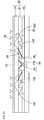
FIG. 45 shows a sectional view of a variation of the disk-shapedsurface plasmon sensor 171 in theembodiment 11. According to this variation, thelight shielding plate 173 is not provided in alight emitting unit 24. Therefore, light L emitted from thelight emitting unit 24 spreads in a plane perpendicular to the upper surface of a lightguide reflection plate 22 and the light L reflected by areflection surface 28 enters the reflection surface region of ametal layer 23 while scattering, and the light L reflected there is received by alight receiving cell 25a in accordance with the reflected angle at the reflection surface region. In addition, alight guide plate 27 having thereflection surface 28 is provided on the lower surface of atransparent substrate 48 in the lightguide reflection plate 22 in this embodiment. - According to this variation, since the divergent light from the
light emitting unit 24 is used, the light L having different reflected angle can be measured at one reflection surface region in themetal layer 23, so that the number of surfaces of the reflection surface region can be reduced. -
FIGs. 46A to 46D show process charts to explain the manufacturing steps of the surface plasmon sensor according to the above variation. As shown inFIG. 46A , aprojection 50 is formed to form thereflection surface 28 on the lower surface of thetransparent substrate 48 by the stamper and arecession 175 is formed to mount thelight emitting unit 24 in the center of the lower surface of thetransparent substrate 48. - Then, as shown in
FIG. 46B , thelight emitting unit 24 is fit in therecession 175. Thelight emitting unit 24 is to be manufactured previously at separate steps by providing a cone-shaped or polygonal cone-shapedreflection plate 172 on the upper surface of a column-shaped or polygonal column-shapedtransparent resin block 176, mounting alight source 29 on the lower surface of thetransparent resin block 176, and providing apolarizing element 30 on the peripheral surface of thetransparent resin block 176. - Then, as shown in
FIG. 46C , thereflection surface 28 is formed by forming a metal film by deposition, etc on the inclined surface of theprojection 50. - Then, as shown in
FIG. 46D , themetal layer 23 including metals such as Au or Ag is formed on the upper surface of thetransparent substrate 48, and thelight guide plate 27 is formed on the lower surface of thetransparent substrate 48 with a transparent resin and thereflection surface 28 is sealed between thelight guide plate 27 and theprojection 50. -
FIG. 47 shows a schematic perspective view of asurface plasmon sensor 181 according to anembodiment 12 of the present invention. According to thesurface plasmon sensor 181, as described in theembodiment 11, a lightguide reflection plate 22 on which ametal layer 23 is formed is rotated by a rotation driving device (not shown) using for example, a motor , etc. Alight receiving element 25 is a one-dimensional light receiving element such as a photodiode array , etc, and it is arranged on the lower surface of the lightguide reflection plate 22 in a resting state along its radius direction. Alight emitting unit 24 used in this case emits radiating light in the plane perpendicular to themetal layer 23, while it emits hardly radiating light in the plane parallel to themetal layer 23. - Thus, according to the
surface plasmon sensor 181, measurement is taken by rotating the lightguide reflection plate 22 on which anantibody 32 is fixed to themetal layer 23. Although only the light L entering from just above thelight receiving element 25 is received by thelight receiving element 25, since the light L for measurement is emitted from the whole lower surface of the lightguide reflection plate 22, the measurement is taken on the whole surface of themetal layer 23 after the lightguide reflection plate 22 is rotated one time. - In addition, a
polarizing element 182 is arranged on thelight receiving element 25 such that only the light L (polarized light) entering from just above thelight receiving element 25 is transmitted. Since polarized direction of the light L entering from the direction other than that from just above thelight receiving element 25 does not coincide with that of thepolarizing element 182, it is not likely to pass through thepolarizing element 182 and not likely to be received by thelight receiving element 25, so that the measurement precision of thepolarizing element 182 is improved. - According to this embodiment, since it is not necessary to provide the
light receiving element 25 so as to correspond to the whole surface of themetal layer 23, thelight receiving element 25 can be inexpensive. Furthermore, since the samelight receiving element 25 andpolarizing element 182 can be used for measurements in the various directions, the measurement is prevented from varying. -
FIG. 48 shows a sectional view of a variation of theembodiment 12. According to this variation, alight shielding plate 184 formed of a light-absorbing material is provided in the center of the lower surface of a lightguide reflection plate 22, and aradiating slit 185 is formed in thelight shielding plate 184. In addition, amirror 183 is provided in the center of the lightguide reflection plate 22. Thus, light L is emitted diagonally upward from thelight emitting unit 24 to the rotating lightguide reflection plate 22. - Thus, when the light L is emitted diagonally upward from the
light emitting unit 24, the light L passes through theslit 185 and inputted to the lightguide reflection plate 22 and it is reflected by themirror 183 and inputted to thereflection surface 28. Then, similar to the case of theembodiment 12, the light L reflected by thereflection surface 28 is inputted to the reflection surface region of themetal layer 23, and the light L reflected by the reflection surface region passes through thepolarizing element 182 and received by thelight receiving element 25. Then, while the lightguide reflection plate 22 on which themetal layer 23 is formed is rotated, the measurement is sequentially performed in the reflection surface regions. - According to the variation, since the light emitted from the
light emitting unit 24 does not spread in the whole direction, but it is emitted only forward like in theembodiment 12, the light L having higher intensity in the center of thelight emitting unit 24 can be effectively used. In addition, as shown inFIG. 48 , when the light L emitted from thelight emitting unit 24 is diverged a little, measurements at different reflected angles in the reflection surface region can be implemented by the light L reflected by the onereflection surface 28 at the same time. In addition, to prevent the light L from being totally reflected by the lower surface of thetransparent substrate 48, a matching oil having a refractive index smaller than thetransparent substrate 48 is applied to the lower surface of thetransparent substrate 48. -
FIG. 49 shows a sectional view of asurface plasmon sensor 191 according to anembodiment 13 of the present invention. According to thesurface plasmon sensor 191, adeflection part 192 in the shape of a triangular prism is provided at the back of areflection surface 28. Thedeflection part 192 is formed of a transparent resin having a refractive index smaller than that of alight guide plate 27 and atransparent substrate 48. Eachdeflection part 192 is arranged such that light L reflected by thereflection surface 28 positioned anterior to it is reflected by ametal layer 23 and then passes through thedeflection part 192, and it is formed such that the angle of the light L after passed through thedeflection part 192, formed with the perpendicular line on the upper surface of thelight receiving element 25 is smaller than that of the light before pass through thedeflection part 192. Alight emitting unit 24 emits the light collimated in the vertical direction only in a fan-like form in a horizontal plane. - Therefore, according to the
surface plasmon sensor 191 of theembodiment 13, since the incident angle of the light L inputting to thelight receiving element 25 can be reduced by means of thedeflection part 192, even when there is no matching oil between a lightguide reflection plate 22 and alight receiving element 25, the light L is prevented from being totally reflected by the lower surface of the lightguide reflection plate 22. As a result, according to this embodiment, it is not necessary to apply the matching oil that is hard to handle, to the lower surface of the lightguide reflection plate 22. -
FIGs. 50A to 50D andFIGs. 51A to 51D show process charts showing one example of the manufacturing steps of the lightguide reflection plate 22 according to theembodiment 13. Although this manufacturing steps are almost the same as those described with reference toFIGs. 9 and10 , according to this embodiment, since amodel 193 of thedeflection part 192 is formed as well as themodel 44 of theprojection 50 in step inFIG. 50B , there is formed arecession 194 for forming thedeflection part 192 as well as arecession 47 for forming the projection in the lower surface of astamper 46 inFIG. 50D . - In addition, since a UV cured
resin 49 having a refractive index smaller than those of thetransparent substrate 48 and thelight guide plate 27 is used inFIG. 51A , thedeflection part 192 having the refractive index smaller than thelight guide plate 27 is formed in the lightguide reflection plate 22 at the steps inFIGs. 51B to 51D . -
FIG. 52 shows a sectional view of a variation of theembodiment 13. According to this variation, adeflection part 192 is formed by a recession (air layer) having a trapezoidal section in the lower surface of atransparent substrate 48. Alight emitting unit 24 emits light collimated in the vertical direction only in a fan-like form in a horizontal plane. -
FIG. 53 shows a sectional view of another variation of theembodiment 13. According to this variation, a matching oil is not needed because adeflection part 192 is provided in the surface plasmon sensor shown inFIG. 45 . However, according to this variation, thedeflection part 192 is formed of a transparent resin having a refractive index higher than that of alight guide plate 27. Alight emitting unit 24 emits light spreading in the vertical direction to whole directions in a horizontal plane. - In addition, when the light emitted from the
light emitting unit 24 is diverged like in this variation or the embodiment shown inFIG. 45 , the light reflected by themetal layer 23 largely spreads. In this case, when the directions of the whole lights are to be bent by onedeflection part 192 having the triangular prism section, thedeflection part 192 becomes thick, which increases the thickness of the surface plasmon sensor. Therefore, according to this variation, thedeflection area 192 is prevented from becoming thick by arranging the plurality ofdeflection parts 192 having the triangular prism sections. - Furthermore,
FIGs. 54A to 54E show process charts showing the manufacturing steps of the surface plasmon sensor according to the variation shown inFIG. 53 . Although the manufacturing steps are almost the same as those shown inFIG. 44 , when thelight guide plate 27 is formed on the upper surface of atransparent substrate 48 in the step inFIG. 54A , arecession 195 for forming thedeflection part 192 in thelight guide plate 27 is formed and thedeflection part 192 is formed by filling therecession 195 with a transparent resin having a refractive index higher than those of thetransparent substrate 48 and thelight guide plate 27 at the step inFIG. 54D . -
FIGs. 55A to 55D show process charts showing other steps for manufacturing the surface plasmon sensor according to the variation shown inFIG. 53 . Although the manufacturing steps are almost the same as those shown inFIG. 46 , thedeflection part 192 is formed, together with theprojection 50, on the lower surface of anauxiliary substrate 174 by a transparent resin having a refractive index higher than those of thetransparent substrate 48, thelight guide plate 27 and theauxiliary substrate 174 at the step inFIG. 55A . In addition, thelight guide plate 27 and thetransparent substrate 48 are formed at the same step. -
FIG. 56 shows a sectional view of still another variation of theembodiment 13. According to this variation, a plurality ofdeflection parts 192 having the shape of triangular prism are provided with a transparent resin or cavities having a refractive index smaller than thelight guide plate 27 in the surface plasmon sensor shown inFIG. 48 . Although thedeflection part 192 is provided in the whole region through which the light passes in this variation also, a lightguide reflection plate 22 is prevented from becoming thick by dividing thedeflection part 192. While alight emitting unit 24 emits radiating light in the plane perpendicular to ametal layer 23, it emits hardly spreading light in the plane parallel to themetal layer 23. -
FIG. 57 shows an outside perspective view of a flow-type analyzer 201 according to the present invention. The flow-type analyzer 201 incorporates asurface plasmon sensor 203 according to the present invention at the upper part of acasing 202 and includes apower supply 204 such as a dry battery at the lower part of thecasing 202, and has anoperation switch 205 for starting an analyzing process, above thepower supply 204. In addition, aliquid crystal display 206 for displaying the guide of an operation method, the progress of the analyzing process, analyzed result , etc is provided above theoperation switch 205. Furthermore, this flow-type analyzer 201 incorporates a small printer and when aprinting switch 207 on the side is pressed, the analyzed result , etc are printed out from aprint result outlet 208 provided beside the switch. -
FIG. 58 shows an exploded perspective view of the structure of thesurface plasmon sensor 203 incorporated in the flow-type analyzer 201. According to thesurface plasmon sensor 203, areplacement component 64 can be detachably set on asensor body 214 and only thesensor body 214 is fixed to thecasing 202. - The
replacement component 64 has a structure in which achannel cover 26 is set on anauxiliary substrate 62 on which ametal layer 23 is formed. A samplesolution supply port 209 for supplying a sample solution is provided in thechannel cover 26, and a samplesolution discharge port 213 for discharging the sample solution after inspected is provided in theauxiliary substrate 62. A supply tube 210 (sample solution supply path),channels 33, a discharge tube 212 (sample solution supply path) are formed between theauxiliary substrate 62 and thechannel cover 26, and one end of thesupply tube 210 is communicated with the samplesolution supply port 209. The other end of thesupply tube 210 is connected to thechannels 33, and the other ends of thechannels 33 are connected to thedischarge tube 212, and the other end of thedischarge tube 212 is connected to the samplesolution discharge port 213. Anantibody holder 211 for positioning and holding anantibody 32 is arranged at a position through which thechannel 33 passes, and thechannel 33 is communicated with theantibody holder 211. Thus, after the sample solution inputted from theupstream channel 33 has spread in theantibody holder 211, it is discharged from thedownstream channel 33. - A
light emitting unit 24, a lightguide reflection plate 22 and alight receiving element 25 are provided in thesensor body 214, and acontroller 216 for controlling the flow-type analyzer 201 is also provided. Furthermore, thesensor body 214 is provided with apump 215 for pumping out the sample solution to the sample solution supply path and thechannels 33, and a collecting tank 217 (refer toFIG. 59 ) for collecting the sample solution after inspected. Thereplacement component 64 is set on thesensor body 214 such that the region on which thechannel 33 and theantibody holder 211 are provided is overlapped on the lightguide reflection plate 22 with a thin matching oil layer sandwiched between them and the samplesolution discharge port 213 is connected to thepump 215. -
FIG. 59 shows a schematic view to explain the operation of the flow-type analyzer 201. Thecontroller 216 includes a light emittingunit driver circuit 218, apump drive circuit 219, adata memory unit 220, and ananalyzer circuit 221. The light emittingunit driver circuit 218 controls thelight emitting unit 24, thepump drive circuit 219 controls thepump 215, and thedata memory unit 220 stores measured data from thelight receiving element 25. - Thus, when the sample solution to be inspected is supplied from the sample
solution supply port 209 and thepump 215 is driven, the sample solution supplied from the samplesolution supply port 209 is suctioned by thepump 215 and flows at a constant flow rate, and the sample solution supplied from thesupply tube 210 to thechannel 33 branches off into eachchannel 33. At this time, when an antigen that is specifically coupled to the antibody fixed to theantibody holder 211 is contained in the sample solution, the antigen is coupled to the antibody. Then, the sample solution that has passed through thechannel 33 is discharged from the samplesolution discharge port 213 through thedischarge tube 212 and discharged into the collectingtank 217 through thepump 215 in thesensor body 214. At this time, thecontroller 216 turns on thelight emitting unit 24 by the light emittingunit drive circuit 218 to emit light to the lightguide reflection plate 22 and reads the light intensity from thelight receiving cell 25a in thelight receiving element 25 and stores it in thedata memory unit 220. - The
analyzer circuit 221 determines whether there is an object to be measured such as a antigen or not and calculates the coupled amount of the object and a time variation of the coupled amount based on the measured data stored in thedata memory unit 220 and outputs the result to theliquid crystal display 206. In addition, when theprint switch 207 is pressed, the measured result is outputted from theprinter 222 and a printed sheet comes out of theprint result outlet 208. After the measurement, thereplacement component 64 is removed from thesensor body 214 and abandoned. -
FIG. 60 shows a schematic view of afingerprint recognition device 231 according to an embodiment of the present invention. Thefingerprint recognition device 231 is provided such that a lightguide reflection plate 22 is put on alight receiving element 25 including a two-dimensional light receiving element such as a CCD or a photodiode array, and the upper surface of the lightguide reflection plate 22 is afingerprint surface 232. Many fine reflection surfaces 28 are arranged in the lightguide reflection plate 22 such that they form a checkered pattern when viewed from the direction perpendicular to thefingerprint surface 232, and an opening for passing light L is provided between thereflection surface 28 and thereflection surface 28. The inclined angle of thereflection surface 28 is equal. In addition, alight emitting unit 24 emits light collimated in the vertical direction only in a fan-like form in a horizontal plane (refer toFIG. 5 or6 ) and arranged such that light emitting surface is at the same level as that of thereflection surface 28. - In addition, when the reflection surfaces 28 are relatively densely arranged like the
surface plasmon sensor 231, the light L is interrupted by thereflection surface 28 positioned closer to thelight emitting unit 24 and not likely to reach therear reflection surface 28. Thus, according to thefingerprint recognition device 231, as shown inFIG. 61 , light guiding reflection surfaces 233 and 234 are formed by forming cavities in alight guide plate 27. When the light L is reflected by the light guiding reflection surfaces 233 and 234, it diverts thereflection surface 28 positioned closer to thelight emitting unit 24 so that the light L is inputted to therear reflection surface 28 in the front direction. - Thus, when the fingerprint is recognized by the
fingerprint recognition device 231, as shown inFIG. 60 , afinger tip 235 is put on thefingerprint surface 232 of thefingerprint recognition device 231 and then the ball of the finger is pressed closely. When the light is emitted from thelight emitting unit 24 in this state, the light reflected by thereflection surface 28 reaches thefingerprint surface 232. Here, when a convex 236 of the fingerprint is closely attached to thefingerprint surface 232 at the inputted point of the light, the light L is reflected here and received by thelight receiving element 25. In addition, when a concave 237 of the fingerprint is closely attached to thefingerprint surface 232 at the inputted point of the light, the light inputted here reaches the concave 237 through thefingerprint surface 232 and scattered here and absorbed. Thus, the light L is hardly reflected by thelight receiving element 25 at the position of the concave 237. Therefore, in thelight receiving element 25, the light receiving amount varies depending on the contour pattern of the fingerprint and the fingerprint pattern is acquired in detail by the different pattern of the light receiving amount. - The light receiving amount pattern is sent to a determining device (not shown) and the determining device determines whether the fingerprint matches with a previously registered fingerprint or not.
- According to the above
fingerprint recognition device 231, the fingerprint can be illuminated by a fewlight sources 29, so that there can be provided thefingerprint recognition device 231 that is thin and has a few components. - In addition, as described in the embodiment 7, since the direction of the light reflected (reflected direction) by the reflection surface can be adjusted relatively freely by the configuration of the reflection surface, the light guiding
reflection surface 234 of the light guiding reflection surfaces 233 and 234 shown inFIG. 61 can be omitted.
Claims (12)
- A surface plasmon sensor that comprises:a light guide reflection plate (22) for guiding light for measurement comprising:a plurality of projections (50) disposed on a first surface, anda plurality of first reflection surfaces (28) inclined with respect to the first surface and disposed on the plurality of projections (50), the plurality of projections (50) being positioned so as not to overlap with each other in the emitting direction of the light on a horizontalplane of the first surface;a surface plasmon resonance layer (23; 62) responsive to an object to be measured, positioned on the first surface and comprising a metal layer (23) which is substantially parallel to the first surface of the light guide reflection plate (22),a light source (29) for emitting the light to said light guide reflection plate (22), the light source (29) being disposed on an end surface located at an end part of the light guide reflection plate (22),a light receiving element (25) disposed on a second surface of the light guide reflection plate (22) opposite the first surface,wherein the light guide reflection plate (22) is transparent to light emitted by the light source (29),
wherein the plurality of first reflection surfaces (28) are configured to reflect the light emitted from the light source (29) toward the surface plasmon resonance layer (23; 62),
wherein the metal layer (23) is configured to reflect the light reflected by the plurality of first reflection surfaces (28),
wherein the light guide reflection plate (22) is transparent to the light reflected by the metal layer (23) and is configured to emit the light out of the second surface to the light receiving element (25), and
wherein the light receiving element (25) is configured to receive the light reflected by the metal layer (23). - The surface plasmon sensor according to claim 1,
wherein a second reflection surface (112) paired with one of the first reflection surfaces (28) is formed in the light guide reflection plate (22),
the first reflection surface (28) is formed in a state inclined toward the direction in which the light source (29) is positioned,
the second reflection surface (112) is inclined to the direction opposite to the direction in which the light source (29) is positioned, and
the first reflection surface (28) and the second reflection surface (112) are arranged such that the light emitted from the light source (29) is reflected by the first reflection surface (28), reflected by the metal layer (23), reflected by the second reflection surface (112) and received by the light receiving element (25). - The surface plasmon sensor according to claim 1,
wherein the first reflection surfaces (28) are curved. - The surface plasmon sensor according to claim 1,
wherein a spectral device (82) is provided between the second surface opposed to the first surface and the light receiving element (25). - The surface plasmon sensor according to claim 1,
wherein a plurality of light sources (29) capable of emitting light sequentially are arranged, and
the plurality of first reflection surfaces (28) are formed such that the light emitted from each light source (29) is reflected by the different reflection surfaces (28), reflected by the metal layer (23) and inputted to a common inputted point in the light receiving element (25). - The surface plasmon sensor according to claim 1,
wherein a single light source (29) is arranged
emitting radiating light in a plane parallel to the surface plasmon resonance layer, and
the plurality of first reflection surfaces (28) are formed such that inputted positions of the light in the light receiving element (25) after emitted from the light source (29), reflected by the different reflection surfaces (28), reflected by the metal layer are aligned in a straight line. - The surface plasmon sensor according to claim 1,
wherein a deflection part (192) is provided in a light path between the position in which the light emitted from the light source (29) and reflected by the first reflection surfaces (28) is reflected by the metal layer (23), and a position in which the light reflected by the metal layer (23) is inputted to the light receiving element (25), and
the deflection part (192) deflects the light path such that the incident angle of the light inputted to the light receiving element (25) becomes small. - The surface plasmon sensor according to claim 1,
wherein a light shielding plate (173, 184) for shielding the light is provided in the light guide reflection plate (22), and
a hole for transmitting the light for measurement is provided in the light shielding plate (173, 184). - The surface plasmon sensor according to claim 1,
wherein a biomolecular recognition substance is fixed to the surface plasmon resonance layer. - A flow-type analyzer comprising:a surface plasmon sensor (21, 61, 71, 81, 91, 101, 111, 121, 131, 141, 151, 161, 171, 181, 191) according to claim 1, anda flow path (33) formed on a surface of the surface plasmon resonance layer (23; 62) opposite to the light guide reflection plate (22), anda sample supply path and a pump for flowing an inspection sample solutions to the flow path (33).
- The flow-type analyzer according to claim 10,
wherein the positions in which the light for measurement is reflected by the metal layer (23) are formed so as to be aligned on the line corresponding to the flow path (33) on the metal layer (23). - The flow-type analyzer according to claim 10,
wherein the surface plasmon resonance layer (23; 62) is provided by depositing a metal film on a transparent auxiliary substrate, and
the surface plasmon resonance layer (23; 62) and the flow path (33) are detachably mounted on the first surface of the light guide reflection plate (22).
Applications Claiming Priority (1)
| Application Number | Priority Date | Filing Date | Title |
|---|---|---|---|
| JP2006071793A JP4893032B2 (en) | 2006-03-15 | 2006-03-15 | Optical component, optical sensor and surface plasmon sensor |
Publications (2)
| Publication Number | Publication Date |
|---|---|
| EP1835277A1 EP1835277A1 (en) | 2007-09-19 |
| EP1835277B1 true EP1835277B1 (en) | 2016-08-10 |
Family
ID=38109576
Family Applications (1)
| Application Number | Title | Priority Date | Filing Date |
|---|---|---|---|
| EP07104262.6A Not-in-force EP1835277B1 (en) | 2006-03-15 | 2007-03-15 | Optical component, optical sensor, surface plasmon sensor and fingerprint recognition device |
Country Status (3)
| Country | Link |
|---|---|
| US (1) | US7692795B2 (en) |
| EP (1) | EP1835277B1 (en) |
| JP (1) | JP4893032B2 (en) |
Families Citing this family (35)
| Publication number | Priority date | Publication date | Assignee | Title |
|---|---|---|---|---|
| JP5252892B2 (en) * | 2007-11-20 | 2013-07-31 | オリンパス株式会社 | Optical unit |
| WO2009090985A1 (en) * | 2008-01-16 | 2009-07-23 | Nippon Telegraph And Telephone Corporation | Flow speed measuring device, antigen concentration measuring device, flow cell, flow speed measuring method, and antigen concentration measuring method |
| WO2009122590A1 (en) * | 2008-04-04 | 2009-10-08 | 国立大学法人琉球大学 | Kit for detecting viral antigen and viral antibody including support storable at room temperature and having viral antigen and viral antibody immobilized thereon, and method for detecting viral antigen and viral antibody |
| JPWO2009122591A1 (en) * | 2008-04-04 | 2011-07-28 | 国立大学法人 琉球大学 | Virus antigen and virus antibody detection kit capable of detecting virus antigen and virus antibody at one time, and virus antigen and virus antibody detection method |
| WO2010024202A1 (en) * | 2008-09-01 | 2010-03-04 | 日立化成工業株式会社 | Spr sensor |
| JP2010236868A (en) * | 2009-03-30 | 2010-10-21 | Sumitomo Electric Ind Ltd | Biological sample fixing sheet and method for producing the same |
| EP3723034B1 (en) * | 2009-10-26 | 2025-04-02 | NEC Corporation | Fake finger determination apparatus and fake finger determination method |
| US8696991B1 (en) | 2010-01-04 | 2014-04-15 | Harold W. Howe | Field deployable surface plasmon resonance based biosensor |
| JPWO2011142118A1 (en) * | 2010-05-12 | 2013-07-22 | パナソニック株式会社 | Plasmon sensor and method of using and manufacturing the same |
| US20140170024A1 (en) * | 2011-07-15 | 2014-06-19 | National Institute Of Advanced Industrial Science And Technology | Target substance detection chip, target substance detection plate, target substance detection device and target substance detection method |
| FR2993987B1 (en) * | 2012-07-26 | 2016-12-09 | Centre Nat Rech Scient | OPTICAL METHODS FOR SAMPLE OBSERVATION AND FOR THE DETECTION OR DETERMINATION OF CHEMICAL OR BIOLOGICAL SPECIES. |
| EP2899532B1 (en) * | 2012-09-19 | 2018-10-24 | Konica Minolta, Inc. | Sensor chip and method for storing sensor chip |
| CN104518835B (en) * | 2013-10-08 | 2019-07-23 | 中兴通讯股份有限公司 | A receiving device of a visible light communication MIMO system |
| US9423345B2 (en) | 2014-06-24 | 2016-08-23 | International Business Machines Corporation | Chemical sensors based on plasmon resonance in graphene |
| US9470632B2 (en) | 2014-07-29 | 2016-10-18 | International Business Machines Corporation | Plasmonic structure with enhanced bandwidth |
| JP2016038395A (en) * | 2014-08-05 | 2016-03-22 | 日東電工株式会社 | Method of light incident upon optical waveguide |
| JP6356563B2 (en) * | 2014-09-29 | 2018-07-11 | 京セラ株式会社 | Optical sensor module |
| US9829614B2 (en) | 2015-02-02 | 2017-11-28 | Synaptics Incorporated | Optical sensor using collimator |
| US9934418B2 (en) | 2015-12-03 | 2018-04-03 | Synaptics Incorporated | Display integrated optical fingerprint sensor with angle limiting reflector |
| US10169630B2 (en) | 2015-12-03 | 2019-01-01 | Synaptics Incorporated | Optical sensor for integration over a display backplane |
| US10176355B2 (en) | 2015-12-03 | 2019-01-08 | Synaptics Incorporated | Optical sensor for integration in a display |
| KR102693504B1 (en) * | 2016-09-26 | 2024-08-12 | 삼성디스플레이 주식회사 | Display device and driving method thereof |
| CN106506741B (en) * | 2016-11-21 | 2020-01-03 | 深圳睿思科信息技术有限公司 | Fingerprint identification module, working method thereof and mobile terminal |
| KR102890456B1 (en) | 2017-02-24 | 2025-11-24 | 삼성전자 주식회사 | Method and electronic device for identifying position of sensor using pixels of display |
| EP3593529B1 (en) * | 2017-03-06 | 2022-07-06 | Gelsight, Inc. | Surface topography measurement systems |
| WO2018190358A1 (en) * | 2017-04-14 | 2018-10-18 | 国立研究開発法人産業技術総合研究所 | Desired-substance detection chip, desired-substance detection device, and desired-substance detection method |
| JP7097563B2 (en) * | 2017-07-13 | 2022-07-08 | 国立研究開発法人産業技術総合研究所 | Target substance detection device and target substance detection method |
| EP3396355A1 (en) * | 2017-04-27 | 2018-10-31 | Pharmafluidics NV | Lateral detection of fluid properties |
| JP6954626B2 (en) * | 2018-04-04 | 2021-10-27 | 国立大学法人 東京大学 | SPR sensor chip, SPR sensor, and sample analysis method |
| US10735634B2 (en) | 2018-06-14 | 2020-08-04 | Gingy Technology Inc. | Image capture apparatus |
| TWI704685B (en) * | 2018-06-14 | 2020-09-11 | 金佶科技股份有限公司 | Image capture apparatus |
| CN109738982B (en) * | 2019-01-31 | 2020-06-23 | 昆山市诚泰电气股份有限公司 | Light guide plate and preparation method thereof |
| CN113161432A (en) * | 2020-01-23 | 2021-07-23 | 群创光电股份有限公司 | Electronic device |
| CN111325192A (en) * | 2020-04-10 | 2020-06-23 | Oppo广东移动通信有限公司 | Backlight module, display screen and electronic equipment |
| JP2024135227A (en) * | 2023-03-22 | 2024-10-04 | 株式会社リコー | Measurement device, surface plasmon resonance sensor, wearable sensor, and manufacturing method. |
Family Cites Families (24)
| Publication number | Priority date | Publication date | Assignee | Title |
|---|---|---|---|---|
| JPS63265142A (en) * | 1986-12-04 | 1988-11-01 | Ricoh Co Ltd | Liquid physical property measurement device |
| DE68907519T2 (en) | 1988-05-10 | 1993-10-21 | Amersham Int Plc | Biosensors. |
| JPH05322747A (en) * | 1992-03-16 | 1993-12-07 | Nippon Telegr & Teleph Corp <Ntt> | Total reflection absorption measuring device |
| US5815278A (en) * | 1995-10-25 | 1998-09-29 | University Of Washington | Surface plasmon resonance light pipe sensing probe and related interface optics |
| EP0797091A1 (en) | 1996-03-19 | 1997-09-24 | Texas Instruments Incorporated | Surface plasmon resonance sensor with interchangable optical element |
| EP0797090A3 (en) | 1996-03-19 | 1997-10-01 | Texas Instruments Incorporated | Integrally formed surface plasmon resonance sensor |
| JPH10300667A (en) * | 1997-04-23 | 1998-11-13 | Shimadzu Corp | Plate and device for measuring molecular interaction |
| JP3380744B2 (en) | 1998-05-19 | 2003-02-24 | 株式会社日立製作所 | Sensor and measuring device using the same |
| JP3465875B2 (en) * | 1998-12-28 | 2003-11-10 | セントラル硝子株式会社 | Raindrop / condensation detector |
| KR20010110428A (en) | 1999-02-01 | 2001-12-13 | 비르 에이/에스 | A surface plasmon resonance sensor |
| JP2001337036A (en) * | 2000-05-25 | 2001-12-07 | Masao Karube | Differential SPR sensor and measuring method using the same |
| CA2407721A1 (en) * | 2000-07-21 | 2002-01-31 | Vir A/S | Coupling elements for surface plasmon resonance sensors |
| JP3576093B2 (en) * | 2000-11-22 | 2004-10-13 | 日本電信電話株式会社 | Optical waveguide type SPR phenomenon measuring device |
| US6862398B2 (en) * | 2001-03-30 | 2005-03-01 | Texas Instruments Incorporated | System for directed molecular interaction in surface plasmon resonance analysis |
| JP2003075337A (en) * | 2001-09-03 | 2003-03-12 | Mitsubishi Heavy Ind Ltd | Integrated surface plasmon resonance sensor |
| DE10151312C2 (en) | 2001-10-17 | 2003-08-28 | Vir As Taastrup | Surface plasmon resonance sensor |
| JP2003262585A (en) * | 2002-03-08 | 2003-09-19 | Stanley Electric Co Ltd | Manufacturing method of surface plasmon resonance sensor |
| EP1509760A1 (en) | 2002-05-31 | 2005-03-02 | Gyros AB | Detector arrangement based on surface plasmon resonance |
| JP2004357721A (en) * | 2003-04-11 | 2004-12-24 | Toshiba Corp | Optical waveguide type invasive device, invasive guidance device and optical waveguide type invasive system |
| DE10324973B4 (en) * | 2003-05-27 | 2006-04-13 | Fraunhofer-Gesellschaft zur Förderung der angewandten Forschung e.V. | Arrangement and method for the optical detection of chemical, biochemical molecules and / or particles contained in samples |
| JP2005049297A (en) * | 2003-07-31 | 2005-02-24 | National Institute Of Advanced Industrial & Technology | Bioelement for photodetection and biodetection method |
| WO2005054826A1 (en) * | 2003-12-08 | 2005-06-16 | Omron Corporation | Optical analyzing unit and optical analyzing device |
| JP4234609B2 (en) * | 2004-01-07 | 2009-03-04 | ローム株式会社 | Surface plasmon resonance sensor |
| JP4777623B2 (en) * | 2004-08-04 | 2011-09-21 | 日本電信電話株式会社 | Biosensor and measurement method |
-
2006
- 2006-03-15 JP JP2006071793A patent/JP4893032B2/en not_active Expired - Fee Related
-
2007
- 2007-03-15 EP EP07104262.6A patent/EP1835277B1/en not_active Not-in-force
- 2007-03-15 US US11/724,681 patent/US7692795B2/en active Active
Also Published As
| Publication number | Publication date |
|---|---|
| US20070222998A1 (en) | 2007-09-27 |
| EP1835277A1 (en) | 2007-09-19 |
| JP4893032B2 (en) | 2012-03-07 |
| US7692795B2 (en) | 2010-04-06 |
| JP2007248253A (en) | 2007-09-27 |
Similar Documents
| Publication | Publication Date | Title |
|---|---|---|
| US7692795B2 (en) | Optical component, optical sensor, surface plasmon sensor and fingerprint recognition device | |
| EP0869351B1 (en) | Measuring chip for optical analyzer | |
| CN108449968B (en) | Handheld field portable surface plasmon resonance device and its application in the detection of chemical and biological reagents | |
| US7342663B2 (en) | Optical analyzing unit and optical analyzing device | |
| JP3064313B2 (en) | Optical interface means | |
| JP5146311B2 (en) | Chip for surface plasmon resonance sensor and surface plasmon resonance sensor | |
| US7879598B2 (en) | Multianalyte determination system and methods | |
| US5764356A (en) | Trace liquid detecting and analyzing device | |
| JP2003524178A (en) | SPR sensor system | |
| JPH05504626A (en) | Sample cell used for chemical or biochemical tests | |
| US7002688B2 (en) | Multilens optical assembly for a diagnostic device | |
| CN103430011B (en) | Measuring device for quantitative optical evaluation of chemical reactions | |
| EP1324019B1 (en) | Sensor utilizing evanescent wave | |
| US20050200853A1 (en) | Analysis method and apparatus and analysis unit | |
| KR20010110428A (en) | A surface plasmon resonance sensor | |
| EP1643254A2 (en) | Sample supplying method and device | |
| US7535570B2 (en) | One dimensional measuring unit having a dielectric block | |
| JPH09196739A (en) | Liquid detection method and device | |
| US7271885B2 (en) | Plasmon resonance measuring method and apparatus | |
| US7218401B2 (en) | Surface plasmon sensor, surface plasmon resonance measurement device, and detection chip | |
| CN102128809A (en) | Surface plasma resonance sensor chip assembly and cylindrical prism chip | |
| CN109612944B (en) | Spectral detection system and spectral detection and analysis method | |
| JP4064169B2 (en) | Sensors using specific substance recovery methods and total reflection attenuation | |
| US8354073B2 (en) | Inspection chip equipped with a light amplifier element | |
| KR20220078703A (en) | Multiplexed Surface Plasmon Resonance Detection of Analytes in Liquid Samples |
Legal Events
| Date | Code | Title | Description |
|---|---|---|---|
| PUAI | Public reference made under article 153(3) epc to a published international application that has entered the european phase |
Free format text: ORIGINAL CODE: 0009012 |
|
| AK | Designated contracting states |
Kind code of ref document: A1 Designated state(s): AT BE BG CH CY CZ DE DK EE ES FI FR GB GR HU IE IS IT LI LT LU LV MC MT NL PL PT RO SE SI SK TR |
|
| AX | Request for extension of the european patent |
Extension state: AL BA HR MK YU |
|
| 17P | Request for examination filed |
Effective date: 20080318 |
|
| 17Q | First examination report despatched |
Effective date: 20080415 |
|
| AKX | Designation fees paid |
Designated state(s): AT BE BG CH CY CZ DE DK EE ES FI FR GB GR HU IE IS IT LI LT LU LV MC MT NL PL PT RO SE SI SK TR |
|
| REG | Reference to a national code |
Ref country code: DE Ref legal event code: R079 Ref document number: 602007047332 Country of ref document: DE Free format text: PREVIOUS MAIN CLASS: G01N0021550000 Ipc: G01N0021552000 |
|
| GRAP | Despatch of communication of intention to grant a patent |
Free format text: ORIGINAL CODE: EPIDOSNIGR1 |
|
| RIC1 | Information provided on ipc code assigned before grant |
Ipc: G06K 9/00 20060101ALI20160215BHEP Ipc: G01N 21/552 20140101AFI20160215BHEP |
|
| INTG | Intention to grant announced |
Effective date: 20160302 |
|
| GRAS | Grant fee paid |
Free format text: ORIGINAL CODE: EPIDOSNIGR3 |
|
| GRAA | (expected) grant |
Free format text: ORIGINAL CODE: 0009210 |
|
| AK | Designated contracting states |
Kind code of ref document: B1 Designated state(s): AT BE BG CH CY CZ DE DK EE ES FI FR GB GR HU IE IS IT LI LT LU LV MC MT NL PL PT RO SE SI SK TR |
|
| REG | Reference to a national code |
Ref country code: GB Ref legal event code: FG4D |
|
| REG | Reference to a national code |
Ref country code: CH Ref legal event code: EP Ref country code: AT Ref legal event code: REF Ref document number: 819504 Country of ref document: AT Kind code of ref document: T Effective date: 20160815 |
|
| REG | Reference to a national code |
Ref country code: IE Ref legal event code: FG4D |
|
| REG | Reference to a national code |
Ref country code: DE Ref legal event code: R096 Ref document number: 602007047332 Country of ref document: DE |
|
| REG | Reference to a national code |
Ref country code: LT Ref legal event code: MG4D |
|
| REG | Reference to a national code |
Ref country code: NL Ref legal event code: MP Effective date: 20160810 |
|
| REG | Reference to a national code |
Ref country code: AT Ref legal event code: MK05 Ref document number: 819504 Country of ref document: AT Kind code of ref document: T Effective date: 20160810 |
|
| PG25 | Lapsed in a contracting state [announced via postgrant information from national office to epo] |
Ref country code: IT Free format text: LAPSE BECAUSE OF FAILURE TO SUBMIT A TRANSLATION OF THE DESCRIPTION OR TO PAY THE FEE WITHIN THE PRESCRIBED TIME-LIMIT Effective date: 20160810 Ref country code: FI Free format text: LAPSE BECAUSE OF FAILURE TO SUBMIT A TRANSLATION OF THE DESCRIPTION OR TO PAY THE FEE WITHIN THE PRESCRIBED TIME-LIMIT Effective date: 20160810 Ref country code: LT Free format text: LAPSE BECAUSE OF FAILURE TO SUBMIT A TRANSLATION OF THE DESCRIPTION OR TO PAY THE FEE WITHIN THE PRESCRIBED TIME-LIMIT Effective date: 20160810 Ref country code: IS Free format text: LAPSE BECAUSE OF FAILURE TO SUBMIT A TRANSLATION OF THE DESCRIPTION OR TO PAY THE FEE WITHIN THE PRESCRIBED TIME-LIMIT Effective date: 20161210 Ref country code: NL Free format text: LAPSE BECAUSE OF FAILURE TO SUBMIT A TRANSLATION OF THE DESCRIPTION OR TO PAY THE FEE WITHIN THE PRESCRIBED TIME-LIMIT Effective date: 20160810 |
|
| PG25 | Lapsed in a contracting state [announced via postgrant information from national office to epo] |
Ref country code: SE Free format text: LAPSE BECAUSE OF FAILURE TO SUBMIT A TRANSLATION OF THE DESCRIPTION OR TO PAY THE FEE WITHIN THE PRESCRIBED TIME-LIMIT Effective date: 20160810 Ref country code: AT Free format text: LAPSE BECAUSE OF FAILURE TO SUBMIT A TRANSLATION OF THE DESCRIPTION OR TO PAY THE FEE WITHIN THE PRESCRIBED TIME-LIMIT Effective date: 20160810 Ref country code: PT Free format text: LAPSE BECAUSE OF FAILURE TO SUBMIT A TRANSLATION OF THE DESCRIPTION OR TO PAY THE FEE WITHIN THE PRESCRIBED TIME-LIMIT Effective date: 20161212 Ref country code: LV Free format text: LAPSE BECAUSE OF FAILURE TO SUBMIT A TRANSLATION OF THE DESCRIPTION OR TO PAY THE FEE WITHIN THE PRESCRIBED TIME-LIMIT Effective date: 20160810 Ref country code: ES Free format text: LAPSE BECAUSE OF FAILURE TO SUBMIT A TRANSLATION OF THE DESCRIPTION OR TO PAY THE FEE WITHIN THE PRESCRIBED TIME-LIMIT Effective date: 20160810 Ref country code: GR Free format text: LAPSE BECAUSE OF FAILURE TO SUBMIT A TRANSLATION OF THE DESCRIPTION OR TO PAY THE FEE WITHIN THE PRESCRIBED TIME-LIMIT Effective date: 20161111 Ref country code: PL Free format text: LAPSE BECAUSE OF FAILURE TO SUBMIT A TRANSLATION OF THE DESCRIPTION OR TO PAY THE FEE WITHIN THE PRESCRIBED TIME-LIMIT Effective date: 20160810 |
|
| REG | Reference to a national code |
Ref country code: FR Ref legal event code: PLFP Year of fee payment: 11 |
|
| PG25 | Lapsed in a contracting state [announced via postgrant information from national office to epo] |
Ref country code: EE Free format text: LAPSE BECAUSE OF FAILURE TO SUBMIT A TRANSLATION OF THE DESCRIPTION OR TO PAY THE FEE WITHIN THE PRESCRIBED TIME-LIMIT Effective date: 20160810 Ref country code: RO Free format text: LAPSE BECAUSE OF FAILURE TO SUBMIT A TRANSLATION OF THE DESCRIPTION OR TO PAY THE FEE WITHIN THE PRESCRIBED TIME-LIMIT Effective date: 20160810 |
|
| REG | Reference to a national code |
Ref country code: DE Ref legal event code: R097 Ref document number: 602007047332 Country of ref document: DE |
|
| PG25 | Lapsed in a contracting state [announced via postgrant information from national office to epo] |
Ref country code: BE Free format text: LAPSE BECAUSE OF FAILURE TO SUBMIT A TRANSLATION OF THE DESCRIPTION OR TO PAY THE FEE WITHIN THE PRESCRIBED TIME-LIMIT Effective date: 20160810 Ref country code: CZ Free format text: LAPSE BECAUSE OF FAILURE TO SUBMIT A TRANSLATION OF THE DESCRIPTION OR TO PAY THE FEE WITHIN THE PRESCRIBED TIME-LIMIT Effective date: 20160810 Ref country code: DK Free format text: LAPSE BECAUSE OF FAILURE TO SUBMIT A TRANSLATION OF THE DESCRIPTION OR TO PAY THE FEE WITHIN THE PRESCRIBED TIME-LIMIT Effective date: 20160810 Ref country code: BG Free format text: LAPSE BECAUSE OF FAILURE TO SUBMIT A TRANSLATION OF THE DESCRIPTION OR TO PAY THE FEE WITHIN THE PRESCRIBED TIME-LIMIT Effective date: 20161110 Ref country code: SK Free format text: LAPSE BECAUSE OF FAILURE TO SUBMIT A TRANSLATION OF THE DESCRIPTION OR TO PAY THE FEE WITHIN THE PRESCRIBED TIME-LIMIT Effective date: 20160810 |
|
| PLBE | No opposition filed within time limit |
Free format text: ORIGINAL CODE: 0009261 |
|
| STAA | Information on the status of an ep patent application or granted ep patent |
Free format text: STATUS: NO OPPOSITION FILED WITHIN TIME LIMIT |
|
| 26N | No opposition filed |
Effective date: 20170511 |
|
| PG25 | Lapsed in a contracting state [announced via postgrant information from national office to epo] |
Ref country code: SI Free format text: LAPSE BECAUSE OF FAILURE TO SUBMIT A TRANSLATION OF THE DESCRIPTION OR TO PAY THE FEE WITHIN THE PRESCRIBED TIME-LIMIT Effective date: 20160810 |
|
| REG | Reference to a national code |
Ref country code: CH Ref legal event code: PL |
|
| GBPC | Gb: european patent ceased through non-payment of renewal fee |
Effective date: 20170315 |
|
| PG25 | Lapsed in a contracting state [announced via postgrant information from national office to epo] |
Ref country code: MC Free format text: LAPSE BECAUSE OF FAILURE TO SUBMIT A TRANSLATION OF THE DESCRIPTION OR TO PAY THE FEE WITHIN THE PRESCRIBED TIME-LIMIT Effective date: 20160810 |
|
| REG | Reference to a national code |
Ref country code: IE Ref legal event code: MM4A |
|
| PG25 | Lapsed in a contracting state [announced via postgrant information from national office to epo] |
Ref country code: LU Free format text: LAPSE BECAUSE OF NON-PAYMENT OF DUE FEES Effective date: 20170315 |
|
| REG | Reference to a national code |
Ref country code: FR Ref legal event code: PLFP Year of fee payment: 12 |
|
| PG25 | Lapsed in a contracting state [announced via postgrant information from national office to epo] |
Ref country code: CH Free format text: LAPSE BECAUSE OF NON-PAYMENT OF DUE FEES Effective date: 20170331 Ref country code: LI Free format text: LAPSE BECAUSE OF NON-PAYMENT OF DUE FEES Effective date: 20170331 Ref country code: IE Free format text: LAPSE BECAUSE OF NON-PAYMENT OF DUE FEES Effective date: 20170315 Ref country code: GB Free format text: LAPSE BECAUSE OF NON-PAYMENT OF DUE FEES Effective date: 20170315 |
|
| PG25 | Lapsed in a contracting state [announced via postgrant information from national office to epo] |
Ref country code: MT Free format text: LAPSE BECAUSE OF NON-PAYMENT OF DUE FEES Effective date: 20170315 |
|
| REG | Reference to a national code |
Ref country code: DE Ref legal event code: R082 Ref document number: 602007047332 Country of ref document: DE Representative=s name: DOMPATENT VON KREISLER SELTING WERNER - PARTNE, DE |
|
| PG25 | Lapsed in a contracting state [announced via postgrant information from national office to epo] |
Ref country code: HU Free format text: LAPSE BECAUSE OF FAILURE TO SUBMIT A TRANSLATION OF THE DESCRIPTION OR TO PAY THE FEE WITHIN THE PRESCRIBED TIME-LIMIT; INVALID AB INITIO Effective date: 20070315 |
|
| PG25 | Lapsed in a contracting state [announced via postgrant information from national office to epo] |
Ref country code: CY Free format text: LAPSE BECAUSE OF NON-PAYMENT OF DUE FEES Effective date: 20160810 |
|
| PG25 | Lapsed in a contracting state [announced via postgrant information from national office to epo] |
Ref country code: TR Free format text: LAPSE BECAUSE OF FAILURE TO SUBMIT A TRANSLATION OF THE DESCRIPTION OR TO PAY THE FEE WITHIN THE PRESCRIBED TIME-LIMIT Effective date: 20160810 |
|
| PGFP | Annual fee paid to national office [announced via postgrant information from national office to epo] |
Ref country code: DE Payment date: 20220203 Year of fee payment: 16 |
|
| PGFP | Annual fee paid to national office [announced via postgrant information from national office to epo] |
Ref country code: FR Payment date: 20220209 Year of fee payment: 16 |
|
| REG | Reference to a national code |
Ref country code: DE Ref legal event code: R119 Ref document number: 602007047332 Country of ref document: DE |
|
| PG25 | Lapsed in a contracting state [announced via postgrant information from national office to epo] |
Ref country code: FR Free format text: LAPSE BECAUSE OF NON-PAYMENT OF DUE FEES Effective date: 20230331 Ref country code: DE Free format text: LAPSE BECAUSE OF NON-PAYMENT OF DUE FEES Effective date: 20231003 |