EP1834407B1 - Digital to analogue conversion - Google Patents
Digital to analogue conversion Download PDFInfo
- Publication number
- EP1834407B1 EP1834407B1 EP05820670A EP05820670A EP1834407B1 EP 1834407 B1 EP1834407 B1 EP 1834407B1 EP 05820670 A EP05820670 A EP 05820670A EP 05820670 A EP05820670 A EP 05820670A EP 1834407 B1 EP1834407 B1 EP 1834407B1
- Authority
- EP
- European Patent Office
- Prior art keywords
- current
- output
- discharge
- signal
- transistor
- Prior art date
- Legal status (The legal status is an assumption and is not a legal conclusion. Google has not performed a legal analysis and makes no representation as to the accuracy of the status listed.)
- Expired - Lifetime
Links
Images


Classifications
-
- H—ELECTRICITY
- H03—ELECTRONIC CIRCUITRY
- H03M—CODING; DECODING; CODE CONVERSION IN GENERAL
- H03M1/00—Analogue/digital conversion; Digital/analogue conversion
- H03M1/66—Digital/analogue converters
- H03M1/74—Simultaneous conversion
-
- H—ELECTRICITY
- H03—ELECTRONIC CIRCUITRY
- H03M—CODING; DECODING; CODE CONVERSION IN GENERAL
- H03M3/00—Conversion of analogue values to or from differential modulation
- H03M3/30—Delta-sigma modulation
- H03M3/322—Continuously compensating for, or preventing, undesired influence of physical parameters
- H03M3/368—Continuously compensating for, or preventing, undesired influence of physical parameters of noise other than the quantisation noise already being shaped inherently by delta-sigma modulators
- H03M3/37—Compensation or reduction of delay or phase error
- H03M3/372—Jitter reduction
-
- H—ELECTRICITY
- H03—ELECTRONIC CIRCUITRY
- H03M—CODING; DECODING; CODE CONVERSION IN GENERAL
- H03M1/00—Analogue/digital conversion; Digital/analogue conversion
- H03M1/06—Continuously compensating for, or preventing, undesired influence of physical parameters
- H03M1/08—Continuously compensating for, or preventing, undesired influence of physical parameters of noise
- H03M1/0836—Continuously compensating for, or preventing, undesired influence of physical parameters of noise of phase error, e.g. jitter
-
- H—ELECTRICITY
- H03—ELECTRONIC CIRCUITRY
- H03M—CODING; DECODING; CODE CONVERSION IN GENERAL
- H03M1/00—Analogue/digital conversion; Digital/analogue conversion
- H03M1/06—Continuously compensating for, or preventing, undesired influence of physical parameters
- H03M1/08—Continuously compensating for, or preventing, undesired influence of physical parameters of noise
-
- H—ELECTRICITY
- H03—ELECTRONIC CIRCUITRY
- H03M—CODING; DECODING; CODE CONVERSION IN GENERAL
- H03M3/00—Conversion of analogue values to or from differential modulation
-
- H—ELECTRICITY
- H03—ELECTRONIC CIRCUITRY
- H03M—CODING; DECODING; CODE CONVERSION IN GENERAL
- H03M3/00—Conversion of analogue values to or from differential modulation
- H03M3/30—Delta-sigma modulation
- H03M3/458—Analogue/digital converters using delta-sigma modulation as an intermediate step
- H03M3/464—Details of the digital/analogue conversion in the feedback path
-
- H—ELECTRICITY
- H03—ELECTRONIC CIRCUITRY
- H03M—CODING; DECODING; CODE CONVERSION IN GENERAL
- H03M3/00—Conversion of analogue values to or from differential modulation
- H03M3/30—Delta-sigma modulation
- H03M3/50—Digital/analogue converters using delta-sigma modulation as an intermediate step
- H03M3/502—Details of the final digital/analogue conversion following the digital delta-sigma modulation
Definitions
- This invention relates generally to circuits and processes for digital to analogue conversion.
- the present invention has particular application to Delta-Sigma converters and to class D amplifiers.
- DS Delta Sigma
- ADCs Analogue to Digital Converters
- DACs Digital to Analogue Converters
- SC modulators switches
- CT Continuous-Time
- SC modulators are widely used in commercial applications as they can be more efficiently realized in the standard CMOS technology and provide a highly controllable design as well as being highly insensitive to clock jitter problems.
- SC modulators are theoretically well understood and studied.
- SC realizations suffer from some problems.
- One of the biggest drawbacks of them is their relatively high power-consumption which arises from their nature, namely that of a switching capacitor.
- the other main problem of SC DS converters is their relatively low-speed nature arising from the fact that the required bandwidth for their op-amps is at least more than five times bigger than the sampling frequency.
- a SC converter needs an anti-aliasing filter at the input of the modulator to prevent aliasing.
- FIG. 1 a general scheme of a CT DS modulator (converter) is shown comprising a loop-filter 111, an n-bit ADC 112 (also called an n-bit quantizer) and an n-bit DAC 113.
- ADC 112 and DAC 113 are clocked; the sampling operation of the converter is performed at the input to ADC 112.
- CT DS converters perform the sampling operation inside the modulator-loop and so shape the sampling error to be out of the bound of interest. Hence, the bandwidth requirements of the op-amps in the converter are reduced. Moreover, as there is no switching inside the loop-filter, the power consumption of the op-amps and the integrators are substantially decreased.
- CT DS converters are described for example in Schreier, and B. Zhang, "Delta-Sigma Modulators employing Continuous-Time Circuitry,” IEEE Transaction on Circuits and Systems-I, Vol. 43, No. 4, pp. 324-332, April 1996 ; O. Shoaei, and M. Snelgrove, "Optimal (bandpass) Continuous-Time Sigma-Delta Modulator,” IEEE International Symposium on Circuits and Systems, Vol. 5, pp. 489-492, June 1994 ; and Robert H. M.
- Clock-jitter predominantly affects SC DS modulators only at the sampling time of the input signal and hence because of the oversampling nature of the modulator its effect is attenuated in the band of interest at the modulator's output by the factor of the OverSampling Ratio (OSR).
- OSR OverSampling Ratio
- clock jitter changes the feedback value by altering the signal pulse-width of the feedback coming to the loop-filter.
- clock jitter in CT DS modulators has in the order of the square of the OSR worse effect than in SC DS modulators and is a severe problem in designing CT DS modulators.
- EP-A-1147609 This problem has been addressed in EP-A-1147609 , which is described below with reference to Figures 2 and 3 .
- the DAC 113 of Figure 1 is replaced by a capacitor that is charged to different reference voltages, depending on the value of the digital signal, and then discharged through a passive or active resistor. Nevertheless further improvements are desirable, particularly in reducing power consumption.
- WO2004/034588 discloses circuits for reducing clock jitter in a CT DS modulator, wherein, for digital to analog conversion, a control voltage is generated by discharging capacitor until the voltage on the capacitor reaches a level determined by a comparator. Problems with this arrangement include excessive power requirements, caused by the waveform of the capacitor, and clock jitter and circuit complexity caused by use of a comparator.
- JP05075468 discloses a circuit for reducing jitter in a DS modulator wherein a capacitor is charged to a reference voltage in a first phase and then exponentially discharged through a transistor in a second phase.
- Class D Amplifiers are also very susceptible to clock jitter (and also power supply variations) because they involve large signal transitions. This is similar to the problem of the feedback DAC in CT DS converters. Suppressing clock jitter is therefore also desired in class D amplifiers to maintain accuracy.
- Class D amplifiers frequently have the load coupled in an H-bridge configuration, where the load output is switched between two reference voltage levels. H-bridges are widely used in hearing-aid devices because of their low-power, low-voltage compatibility. Using one battery cell, the output of the amplifier is switched between the ground and power supply rails. Clock jitter causes an additional noise floor on the output signal as it changes the duration of on and off switches. Also, switching the output load causes variations on the two rails and therefore decreases the dynamic range and precision of the amplifier.
- the present invention addresses the need for suppression or reduction of the effect of clock-jitter in CT DS modulators and class D amplifiers.
- the present invention provides an apparatus for a digital to analogue conversion of an input signal ( D o ) to an output signal ( U d, OUT) including:
- a method for CT DS modulation of an input signal U i includes: receiving the input signal U i and a feedback signal U d by a continuous-time loop-filter and producing an analogue signal U f , sampling and quantizing the loop-filter's output signal U f to produce a DS modulated signal Do, converting the signal Do to the analogue signal U d that includes:
- a method for a digital to analogue conversion of a signal Do includes:
- an apparatus for CT DS modulation includes: a continuous-time loop-filter receiving an input signal U i and a feedback signal U d to produce an analogue signal U f , a quantizer coupled to receive the loop-filter's output signal U f and produce a DS modulated signal D o , a DAC which includes:
- an apparatus for a digital to analogue conversion of an input signal Do includes:
- the size of the capacitor, the reference voltage, the switches and the transistors should be properly set to ensure that clock jitter has a minimal effect on the integral of the analogue output signal U d undertaken at the second phase.
- a CT DS modulator including, a continuous-time loop-filter receiving an input signal U i and a feedback signal U d to produce an analogue signal U f , a quantizer coupled to receive the loop-filter's output signal U f and produce a DS modulated signal Do, a DAC to produce the analogue signal U d which includes:
- a digital to analogue conversion of an input signal D o including:
- a method for driving a class D amplifier (either single-ended or double-ended which its output is switched between two reference levels) of an input signal Do includes:
- an apparatus for driving a class D amplifier (either single-ended or double-ended which its output is switched between two reference levels) of an input signal Do includes:
- a capacitor 214 is charged to one of the two reference voltages (either + V ref or - V ref ) depending on the digital output of the modulator, Do.
- the capacitor 214 discharges to a resistor 216.
- the capacitor should be essentially fully charged before the end of the first phase ( ⁇ 1 ) and essentially fully discharged before the end of the second phase ( ⁇ 2 ). Having this, the mentioned technique reduces the clock-jitter sensitivity of the modulator, since the integral of the DAC's output voltage undertaken at the second phase ( ⁇ 2 ) is highly independent of the clock transition times.
- the present invention benefits from the behavior of a biased-transistor in the saturation and triode regions.
- CMOS technology in the saturation region of a transistor, regardless of the drain-to-source voltage, the drain-to-source current is almost constant.
- the transistor goes to the triode region, it acts as a resistor and its drain-to-source voltage diminishes to zero. Therefore, if a capacitor is discharged through a biased-transistor, one can expect a current shape like a pulse with an exponential shape in its falling edge like the current shape 313 in FIG. 3 .
- a constant amount of charge is stored in a capacitor and then it discharges through a biased-transistor. The output will therefore be a function of the transistor's current.
- the size of the transistors, capacitor, switches and reference voltages should be set properly to ensure that the output signal meets two criteria:
- the output signal should fall to a low enough level before the end of the phase (T n in FIG. 3 ) to ensure that the clock transition time has a minimal effect on the output's integral.
- the clock jitter effect in the CT DS modulator will be suppressed to a similar level in comparison to its SC counterpart.
- Such a technique can be used to drive a class D amplifier (either single-ended or double-ended) which suffers from clock jitter and output-rails variations.
- Clock jitter suppression is the same as for the CT DS modulation mentioned above.
- the effects of output-rail variations on the output load can also be compensated by making the biased-transistor current a function of the difference between the two output rails.
- ADC 112 and DAC 113 in a CT DS modulator shown in FIG. 1 can be multibit or single-bit.
- single-bit version of them is considered.
- the present invention can be used in both single-bit and multibit CT DS modulator.
- the present invention could be realized in BJT, CMOS and other technologies, the embodiments below are implemented in CMOS technology.
- FIG. 4 shows a first embodiment of the invention that can be used to replace the DAC 113 of the CT DS modulator in FIG. 1 .
- a switched-current DAC has been preferred in the realization as it is largely used in CT DS modulators.
- a control block 410 provides a control current I ref2 for controlling a switched-current block 421.
- Block 410 includes a capacitor 414, coupling switches 412, 413, NMOS transistors 416, 417, 418, 419 and a current source 415.
- the sampling clock of the CT DS modulator in FIG. 1 has two phases ⁇ 1 and ⁇ 2 .
- ⁇ 1 the capacitor 414 is charged to a reference signal V ref via the switch 412 which is controlled as a function of ⁇ 1 .
- the size of the switch 412 and the capacitor 414 should be chosen such that the capacitor 414 is charged to a level beyond which clock jitter will not decrease the desired SNDR of the modulator.
- the capacitor 414 is discharged through a transistor 417 which is cascoded by a transistor 416.
- This cascode tail 420 in parallel with a tail of two diode-connected transistors 418 and 419 and a current-source 415 constitute a cascode current-mirror.
- the transistors 416 and 417 are biased such that in saturation region, their drain-to-source currents I ref1 is a multiple of the current ( I ref0 ) of the current-source 415.
- the transistors 416 and 417 are in saturation region and remain in this mode until the voltage across the capacitor, which is linearly decreasing, meets the saturation voltage of the tail 420. After that, the cascode tail 420 will go to the triode region and exponentially discharge the capacitor 414.
- a switched-current block 421 is used.
- a transistor 422 is used in which its gate is coupled to the source of the transistor 416.
- the transistor 422 acts as a mirror transistor of the transistors 417 or 419.
- the transistor 422's current (Iref2) is a multiple of the Iref0 or Iref1.
- Iref2 is used as a reference current for the switched-current block 421.
- the realization of the switched-current block 421 could be different.
- FIG. 4 a simple single-ended version of a switched-current circuit is realized. Having the transistor 422 as the current reference, the output analogue signals (I+ and I-) are produced as a function of the digital signal Do using switches 424 and 425 which are working as a function of Do. In the case of a CT DS modulator, the output analogue signals (I+ and I-) of the present embodiment feed to the loop-filter 111 as the signal Ud in FIG. 1 .
- FIG. 5 shows a second embodiment of the invention. Similar parts to those of Figure 4 are denoted by the same reference numeral.
- a fully differential switched-current block 441 is employed, which is commonly, used in CT DS modulators. Via a tail consisting of the transistors 430,431 and 432, the current Iref2 is mirrored to a transistor 433 which is the differential pair of the transistor 422. Having the transistors 422 and 433 as the current references, the output analogue signals (I+ and I-) are produced as a function of the digital signal Do using switches 424,425,426 and 427 which are working as a function of Do. In the case of CT DS modulator, the output analogue signals (I+ and I-) of the present embodiment feed to the loop-filter 111 as the signal Ud in FIG. 1 .
- the embodiment's output analogue-current 313 is a pulse shape as expected.
- the pulse amplitude of this analogue current (I n ) is slightly bigger than I t from the ordinary switched-current DAC since the integral of them undertaken at the second phase should be the same.
- the size of the capacitor 414, the analogue reference voltage V ref , the current reference 415, the cascode current mirror's transistors (416, 417, 418, 419) and the switches 412, 413 should be set properly to ensure that the output current 313 falls sufficiently before the clock transition so that the variation of the clock transition (clock jitter) has a minimal effect on the integral of the analogue output current I ref2 undertaken at the second phase.
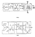
- FIG. 6 shows a block diagram of a third embodiment of the invention including a class D amplifier.
- the block 410 in Figure 6 is similar to block 410 of Figures 4,5 .
- the only difference between the block 410 in FIG. 6 with the one in FIG. 5 is that here the reference current I ref0 is not constant and comes from the feedback made directly proportional to the difference between the two output rails of the class D amplifier (either single-ended or double-ended).
- the output of block 410 and the digital input signal Do enter to the interface block 612 which drives the class D amplifier, 613.
- the output of block 613 is switched between the two reference voltages.
- the output rails are the power supply and the ground terminals.
- these two rails are Vdd and Vss . Because of switching the output load between these two rails, Vdd and Vss are contaminated with some unwanted variations. As the output power is directly proportional to the difference between these two rails, these deviations decrease the accuracy and precision of the amplifier. To reduce these affects and more importantly bring the nonlinear system to its linear region, the feedback block diagram 611 is located to produce the reference current I ref0 as a function of the difference between Vdd and Vss . This current is fed to the block 410 to be used as the reference current.
- FIG. 7 shows a further block diagram of the third embodiment of the invention including a class D amplifier, showing exemplary circuit implementations, and similar parts to those of Figure 6 are denoted by the same reference numeral.
- the block 410 in Figure 7 is similar to block 410 of Figures 4,5 and 6 . Similar to block 410 in Fig. 6 , the reference current I ref0 in block 410 in Fig. 7 is not constant and comes from the feedback made directly proportional to the difference between the two output rails V dd , V ss of the class D amplifier using transconductance amplifier 611.
- the analogue output OUT of block 410 enters to the interface block 612 and is digitised by a comparator 712.
- Class D block 613 in Fig. 7 is an H-bridge, a simple exemplary realization of the class D amplifier block 613 in Fig. 6 (other realisations are possible, for example a push-pull arrangement).
- the H-bridge comprises four switches 724, 725, 726 and 727 with the control digital inputs D l and D h coming from block 612.
- the output load of this H-bridge, 613 is switched between the two reference voltages (here Vdd and Vss). Similar to Fig.
- transconductance amplifier 611 is arranged to produce the reference current I ref0 as a function of the difference between Vdd and Vss . This current is fed to the block 410 to be used as the reference current.
- the Class D amplifier may be double ended, in the sense that it is fully differential and has double output nodes, or single ended, with a single output node.
- the clock signal should at least have two phases.
- first phase and second phase of the clock signal, as used herein, does not imply that the clock signal of the circuit must have only two phases.
Landscapes
- Engineering & Computer Science (AREA)
- Theoretical Computer Science (AREA)
- Compression, Expansion, Code Conversion, And Decoders (AREA)
- Amplifiers (AREA)
- Analogue/Digital Conversion (AREA)
- Transmission Systems Not Characterized By The Medium Used For Transmission (AREA)
- Stabilization Of Oscillater, Synchronisation, Frequency Synthesizers (AREA)
- Control Of Eletrric Generators (AREA)
- Gyroscopes (AREA)
Abstract
Description
- This invention relates generally to circuits and processes for digital to analogue conversion. The present invention has particular application to Delta-Sigma converters and to class D amplifiers.
- Delta Sigma (DS) Analogue to Digital Converters (ADCs) and Digital to Analogue Converters (DACs) have become very popular converters for high-resolution applications because of their oversampling and noise shaping nature. These characteristics make them more robust to their components' nonlinearities and nonidealities. Indeed, by trading accuracy with speed, DS converters have become more attractive in the context of present CMOS technology evolution.
- DS converters can be realized in either Switched-Capacitor (SC) or Continuous-Time (CT) approach. Nowadays, SC modulators (converters) are widely used in commercial applications as they can be more efficiently realized in the standard CMOS technology and provide a highly controllable design as well as being highly insensitive to clock jitter problems. Indeed, SC modulators are theoretically well understood and studied. However, SC realizations suffer from some problems. One of the biggest drawbacks of them is their relatively high power-consumption which arises from their nature, namely that of a switching capacitor. The other main problem of SC DS converters is their relatively low-speed nature arising from the fact that the required bandwidth for their op-amps is at least more than five times bigger than the sampling frequency. Also, a SC converter needs an anti-aliasing filter at the input of the modulator to prevent aliasing.
- Referring to
FIG. 1 , a general scheme of a CT DS modulator (converter) is shown comprising a loop-filter 111, an n-bit ADC 112 (also called an n-bit quantizer) and an n-bit DAC 113. ADC 112 andDAC 113 are clocked; the sampling operation of the converter is performed at the input toADC 112. In contrast to SC DS converters, CT DS converters perform the sampling operation inside the modulator-loop and so shape the sampling error to be out of the bound of interest. Hence, the bandwidth requirements of the op-amps in the converter are reduced. Moreover, as there is no switching inside the loop-filter, the power consumption of the op-amps and the integrators are substantially decreased. These characteristics make CT DS converters more suitable for high-speed applications. CT DS converters are described for example in Schreier, and B. Zhang, "Delta-Sigma Modulators employing Continuous-Time Circuitry," IEEE Transaction on Circuits and Systems-I, Vol. 43, No. 4, pp. 324-332, April 1996; O. Shoaei, and M. Snelgrove, "Optimal (bandpass) Continuous-Time Sigma-Delta Modulator," IEEE International Symposium on Circuits and Systems, Vol. 5, pp. 489-492, June 1994; and Robert H. M. van Veldhoven, "A Triple-Mode Continuous-Time Sigma-Delta Modulator With Switched-Capacitor Feedback DAC for a GSM-EDGE/CDMA200/UMTS Receiver," IEEE Journal of Solid-State Circuits, Vol. 38, No. 12, pp. 2069-2076, December 2003. - Besides the advantages of CT circuitry with respect to their higher bandwidth and/or lower power-dissipation, there are some limitations in achieving high Signal-to-Noise-plus-Distortion ratio (SNDR) from them. The asymmetry of falling and rising edges of the feedback signal, sensitivity to feedback-delay and susceptibility to clock jitter are the biggest obstacles in designing CT DS modulators. Yet, the first two problems have been studied well and some robust techniques and solutions have been proposed to resolve them.
- Clock-jitter predominantly affects SC DS modulators only at the sampling time of the input signal and hence because of the oversampling nature of the modulator its effect is attenuated in the band of interest at the modulator's output by the factor of the OverSampling Ratio (OSR). However, in CT DS modulators, clock jitter changes the feedback value by altering the signal pulse-width of the feedback coming to the loop-filter. Approximately, clock jitter in CT DS modulators has in the order of the square of the OSR worse effect than in SC DS modulators and is a severe problem in designing CT DS modulators.
- This problem has been addressed in
EP-A-1147609 , which is described below with reference toFigures 2 and3 . InEP-A-1147609 , theDAC 113 ofFigure 1 is replaced by a capacitor that is charged to different reference voltages, depending on the value of the digital signal, and then discharged through a passive or active resistor. Nevertheless further improvements are desirable, particularly in reducing power consumption. -
WO2004/034588 discloses circuits for reducing clock jitter in a CT DS modulator, wherein, for digital to analog conversion, a control voltage is generated by discharging capacitor until the voltage on the capacitor reaches a level determined by a comparator. Problems with this arrangement include excessive power requirements, caused by the waveform of the capacitor, and clock jitter and circuit complexity caused by use of a comparator. -
JP05075468 - Class D Amplifiers are also very susceptible to clock jitter (and also power supply variations) because they involve large signal transitions. This is similar to the problem of the feedback DAC in CT DS converters. Suppressing clock jitter is therefore also desired in class D amplifiers to maintain accuracy. Class D amplifiers frequently have the load coupled in an H-bridge configuration, where the load output is switched between two reference voltage levels. H-bridges are widely used in hearing-aid devices because of their low-power, low-voltage compatibility. Using one battery cell, the output of the amplifier is switched between the ground and power supply rails. Clock jitter causes an additional noise floor on the output signal as it changes the duration of on and off switches. Also, switching the output load causes variations on the two rails and therefore decreases the dynamic range and precision of the amplifier.
- Therefore, a need exists to have improved techniques for suppressing clock-jitter in CT DS modulators and also in class D amplifiers.
- The present invention addresses the need for suppression or reduction of the effect of clock-jitter in CT DS modulators and class D amplifiers.
- The present invention provides an apparatus for a digital to analogue conversion of an input signal (Do) to an output signal (Ud, OUT) including:
- capacitance means coupled to a switch means for charging the capacitance means to a reference voltage value (Vref) during a first phase (ϕ1) of a clock signal, and for discharging the capacitance means through a discharge means during a second phase (ϕ2) of the clock signal, said discharge means regulating the discharge of the capacitance means,
- characterized in that said discharge means provides a discharge path including discharge transistor means, wherein the voltage across said capacitance means determines the operating mode of said transistor means such that in said second phase said transistor means operates in a first mode to provide an approximately constant discharge current, and subsequently operates in a second mode for discharging the capacitance means before the end of the second phase; and
- output means coupled to the discharge means for producing said output signal (Ud , OUT) as a function of the discharge current and the input signal (Do ).
- As preferred the transistor means is biased into a saturation mode for providing a constant discharge current, in which case the degree of variation from a constant value will be determined by the characteristics of the saturation mode. The low impedance mode of the transistor means is desirably what is usually known as the triode region of the operating characteristics.
- In the case where the apparatus of the invention is incorporated in a digital to analog converter in a CTDS modulator, the output means may a switched current block, or other means for providing an appropriate signal to a loop filter.
- In the case where the apparatus of the invention is employed in combination with a class D amplifier, the output means may be a Class D amplifier, or a means providing a class D amplifier function
- In accordance with a first specific aspect of the present invention, a method for CT DS modulation of an input signal Ui includes: receiving the input signal Ui and a feedback signal Ud by a continuous-time loop-filter and producing an analogue signal Uf , sampling and quantizing the loop-filter's output signal Uf to produce a DS modulated signal Do, converting the signal Do to the analogue signal Ud that includes:
- a) charging a capacitor to a single analogue reference signal during the first phase of the clock signal (the capacitor should be fully charged during the first phase),
- b) discharging the capacitor through a transistor during the second phase of the clock signal. The transistor is biased to have a desired current Iref1 during its saturation mode,
- c) generating current or voltage sources as a function of the current Iref1 of the transistor,
- d) producing the analogue output Ud as a function of the current or the voltage sources and the DS modulated signal Do and feeding it to the loop-filter as the modulation feedback,
- In accordance with a specific second aspect of the present invention, a method for a digital to analogue conversion of a signal Do includes:
- a) charging a capacitor to a single analogue reference signal during the first phase of the clock signal (the capacitor should be fully charged during the first phase),
- b) discharging the capacitor through a transistor during the second phase of the clock signal. The transistor is biased to have a desired current Iref1 during its saturation mode,
- c) generating current or voltage sources as a function of the current Iref1 of the transistor,
- d) producing an analogue output Ud as a function of the current or the voltage sources and the input signal Do and feeding it to the loop-filter,
- In accordance with a specific third aspect of the present invention, an apparatus for CT DS modulation includes: a continuous-time loop-filter receiving an input signal Ui and a feedback signal Ud to produce an analogue signal Uf , a quantizer coupled to receive the loop-filter's output signal Uf and produce a DS modulated signal Do , a DAC which includes:
- a) a capacitor which one of its two plates is preferably connected to the ground terminal,
- b) a switch coupled to the capacitor charging it to a single analogue reference signal during the first phase of the clock signal,
- c) a switch coupled to the capacitor discharging the capacitor through a transistor during the second phase of the clock signal. The transistor is biased to have a desired current Iref1 during its saturation mode,
- d) current or voltage sources controlled as a function of the transistor current Iref1 ,
- e) a block producing the analogue output Ud as a function of the current or the voltage sources and the DS modulated signal Do and feeding it to the loop-filter as the modulation feedback,
- In accordance with a specific fourth aspect of the present invention, an apparatus for a digital to analogue conversion of an input signal Do includes:
- a) a capacitor which one of its two plates is preferably connected to the ground terminal,
- b) a switch coupled to the capacitor charging it to a single analogue reference signal during the first phase of the clock signal,
- c) a switch coupled to the capacitor discharging the capacitor through a transistor during the second phase of the clock signal. The transistor is biased to have a desired current Iref1 during its saturation mode,
- d) current or voltage sources controlled as a function of the transistor current Iref1.
- e) a block producing an analogue output Ud as a function of the current or the voltage sources and the input signal Do,
- In all of these four aspects, the size of the capacitor, the reference voltage, the switches and the transistors should be properly set to ensure that clock jitter has a minimal effect on the integral of the analogue output signal Ud undertaken at the second phase.
- In accordance with a specific fifth aspect of the present invention, a CT DS modulator is provided including, a continuous-time loop-filter receiving an input signal Ui and a feedback signal Ud to produce an analogue signal Uf , a quantizer coupled to receive the loop-filter's output signal Uf and produce a DS modulated signal Do, a DAC to produce the analogue signal Ud which includes:
- a) means for charging a capacitor to a single analogue reference during the first phase of the clock signal,
- b) means for discharging the capacitor to a biased-transistor during the second phase of the clock signal,
- c) means for generating current or voltage sources controlled as a function of the transistor current,
- d) means for producing the analogue output Ud as a function of the current or the voltage sources and the DS modulated signal Do and feeding it to the loop-filter as the modulation feedback,
- In accordance with a sixth aspect of the present invention, a digital to analogue conversion of an input signal Do is provided including:
- a) means for charging a capacitor to a single analogue reference during the first phase of the clock signal,
- b) means for discharging the capacitor to a biased-transistor during the second phase of the clock signal,
- c) means for generating current or voltage sources controlled as a function of the transistor current Iref1 ,
- d) means for producing an analogue output Ud as a function of the current or the voltage sources and the input signal Do,
- In accordance with a specific seventh aspect of the present invention, a method for driving a class D amplifier (either single-ended or double-ended which its output is switched between two reference levels) of an input signal Do includes:
- a) charging a capacitor to a single analogue reference signal during the first phase of the clock signal (the capacitor should be fully charged during the first phase),
- b) discharging the capacitor through a transistor during the second phase of the clock signal. The transistor is biased to have a current Iref1 during its saturation mode where Iref1 is made directly proportional to the difference between the two output reference levels,
- c) coupling the class D amplifier to the system such that its output signal is a function of the current Iref1 and the input signal Do .
- In accordance with a specific eighth aspect of the present invention, an apparatus for driving a class D amplifier (either single-ended or double-ended which its output is switched between two reference levels) of an input signal Do includes:
- a) means for charging a capacitor to a single analogue reference during the first phase of the clock signal,
- b) means for discharging the capacitor to a biased-transistor during the second phase of the clock signal wherein the biased-transistor's current is made directly proportional to the difference between the two output reference levels,
- c) means for producing an output signal of the coupled class D amplifier as a function of the biased-transistor's current and the input signal Do.
- Preferred embodiments of the invention will now be described with reference to the accompanying drawings, wherein:
- FIG. 1
- shows a prior art CT delta-sigma modulator;
- FIG. 2
- shows a prior art technique for suppressing the clock-jitter in continuous-time delta-sigma modulators;
- FIG. 3
- is a graph comparing the output current of the a priori art switched-current feedback, a prior art technique of suppressing clock-jitter, and the present invention;
- FIG. 4
- shows a circuit diagram of a technique to suppress clock-jitter in a DAC of a CTDS using a switched-current block according to a first embodiment of the present invention;
- FIG. 5
- shows a circuit diagram of a technique to suppress clock-jitter using a fully differential switched-current block according to a second embodiment of the present invention;
- FIG. 6
- shows a block diagram of a technique to suppress clock-jitter and output-rails variations of a class D amplifier according to a third embodiment of the present invention; and
- FIG. 7
- is a further block diagram of the third embodiment of
Figure 6 , showing exemplary circuit implementations. - There is a penalty to pay when deploying a technique to suppress clock-jitter in CT DS modulators. This is, most probably, in the way of some extra power consumption not only in the apparatus circuits but also in the loop-filter of the modulator. Therefore there is a tradeoff between the extra power consumption and the suppression of clock-jitter. In
EP-A-1147609 a technique has been proposed to suppress the sensitivity of CT DS modulators to clock jitter. One of the embodiments of this technique which is a replacement ofDAC 113 inFIG. 1 is shown inFIG. 2 . In this method, the sampling clock has two clock phases Φ1 and Φ2. During the first phase (Φ1), acapacitor 214 is charged to one of the two reference voltages (either + Vref or - Vref ) depending on the digital output of the modulator, Do. During the second phase (Φ2), thecapacitor 214 discharges to aresistor 216. The capacitor should be essentially fully charged before the end of the first phase (Φ1) and essentially fully discharged before the end of the second phase (Φ2). Having this, the mentioned technique reduces the clock-jitter sensitivity of the modulator, since the integral of the DAC's output voltage undertaken at the second phase (Φ2) is highly independent of the clock transition times. - Although this technique suppresses the clock-jitter noise at the output of the modulator, it has some drawbacks. The main problem of this architecture is the increase in the power consumption of the integrator which it feeds. It is essential that the integral of the analogue feedback signal undertaken in each clock period is the same as the integral of the one in the ordinary CT counterpart (for example the switched-current feedback). Hence, due to the exponential shape of the analogue feedback of this technique, and considering the pulsing shape of the switched-current feedback, it can be easily seen by those skilled in the art that the peak of the current feeding to the integrator by the feedback in this technique is much bigger that the one in the switched-current feedback. This phenomenon is demonstrated in
FIG. 3 wherein the current shape in this technique (312) with the peak of Ip is compared to the current shape of a typical switched-current feedback (311) with the amplitude of It. For instance, if at the end of the second phase (Φ2), the feeding current is around one percent of the one in switched-current 311 (It), the peak of the current in this technique (IP ) is more than six times bigger than the one in the switched-current 311 (It). Indeed, this technique uses the SC feedback and requires an integrator with a higher slew-rate and bandwidth than in ordinary CT feedback. - Therefore, a need still exists for a technique for suppressing the clock-jitter in CT DS modulators that is more power efficient.
- The present invention, benefits from the behavior of a biased-transistor in the saturation and triode regions. For example, in CMOS technology, in the saturation region of a transistor, regardless of the drain-to-source voltage, the drain-to-source current is almost constant. When the transistor goes to the triode region, it acts as a resistor and its drain-to-source voltage diminishes to zero. Therefore, if a capacitor is discharged through a biased-transistor, one can expect a current shape like a pulse with an exponential shape in its falling edge like the
current shape 313 inFIG. 3 . As a simple explanation of the present invention, first a constant amount of charge is stored in a capacitor and then it discharges through a biased-transistor. The output will therefore be a function of the transistor's current. The size of the transistors, capacitor, switches and reference voltages should be set properly to ensure that the output signal meets two criteria: - First, the output signal should fall to a low enough level before the end of the phase (Tn in
FIG. 3 ) to ensure that the clock transition time has a minimal effect on the output's integral. By meeting this criterion, the clock jitter effect in the CT DS modulator will be suppressed to a similar level in comparison to its SC counterpart. - ■ Second, the falling edge of the output signal should arrive just before (and not too early) the end of the phase (Tn in
FIG. 3 ). If the output signal goes down too early, although the clock jitter has a minimal effect on the integral of the output signal, the output signal's amplitude (In inFIG. 3 ) should be increased to have the equivalent output signal's integral. The bigger the output signal, the more power consumption in the modulator. - Such a technique can be used to drive a class D amplifier (either single-ended or double-ended) which suffers from clock jitter and output-rails variations. Clock jitter suppression is the same as for the CT DS modulation mentioned above. The effects of output-rail variations on the output load can also be compensated by making the biased-transistor current a function of the difference between the two output rails.
- Some specific embodiments of the present invention are further described to facilitate an understanding of the ways in which the invention may be realized and practiced. The examples can be considered as the preferred embodiments as they are discovered to function well in the practice of the invention. However, it should be appreciated that many changes can be made in the following exemplary embodiments without departing from the invention claimed. Accordingly, the following embodiments should not be considered as limitations on the present invention.
-
ADC 112 andDAC 113 in a CT DS modulator shown inFIG. 1 can be multibit or single-bit. For the sake of simplicity, in the following embodiments single-bit version of them is considered. However, those skilled in the art will appreciate that the present invention can be used in both single-bit and multibit CT DS modulator. Moreover, although the present invention could be realized in BJT, CMOS and other technologies, the embodiments below are implemented in CMOS technology. -
FIG. 4 shows a first embodiment of the invention that can be used to replace theDAC 113 of the CT DS modulator inFIG. 1 . In this embodiment, a switched-current DAC has been preferred in the realization as it is largely used in CT DS modulators. - A
control block 410 provides a control current Iref2 for controlling a switched-current block 421.Block 410 includes acapacitor 414, coupling switches 412, 413,NMOS transistors current source 415. The sampling clock of the CT DS modulator inFIG. 1 has two phases Φ1 and Φ2. During the first phase, Φ1, thecapacitor 414 is charged to a reference signal Vref via theswitch 412 which is controlled as a function of Φ1. The size of theswitch 412 and thecapacitor 414 should be chosen such that thecapacitor 414 is charged to a level beyond which clock jitter will not decrease the desired SNDR of the modulator. - During the second phase, Φ2, via a
switch 413 controlled as a function of Φ2, thecapacitor 414 is discharged through atransistor 417 which is cascoded by atransistor 416. This cascode tail 420 in parallel with a tail of two diode-connectedtransistors source 415 constitute a cascode current-mirror. As it is shown inFIG. 4 , thetransistors source 415. At the start of the discharging of thecapacitor 414 at the second phase, (2, thetransistors capacitor 414. - To produce the output current of the DAC, a switched-
current block 421 is used. To mirror and sense the current of the tail 420, atransistor 422 is used in which its gate is coupled to the source of thetransistor 416. Thetransistor 422 acts as a mirror transistor of thetransistors transistor 422's current (Iref2) is a multiple of the Iref0 or Iref1. When the cascade tail 420 starts to go to its triode region, thetransistor 422 starts to turn off causing its current Iref2 to drop off to zero. The current Iref2 is used as a reference current for the switched-current block 421. The realization of the switched-current block 421 could be different. For the sake of simplicity, inFIG. 4 , a simple single-ended version of a switched-current circuit is realized. Having thetransistor 422 as the current reference, the output analogue signals (I+ and I-) are produced as a function of the digital signal Do usingswitches filter 111 as the signal Ud inFIG. 1 . -
FIG. 5 shows a second embodiment of the invention. Similar parts to those ofFigure 4 are denoted by the same reference numeral. InFigure 5 , a fully differential switched-current block 441 is employed, which is commonly, used in CT DS modulators. Via a tail consisting of the transistors 430,431 and 432, the current Iref2 is mirrored to atransistor 433 which is the differential pair of thetransistor 422. Having thetransistors filter 111 as the signal Ud inFIG. 1 . - As shown in
FIG. 3 , the embodiment's output analogue-current 313 is a pulse shape as expected. The pulse amplitude of this analogue current (In) is slightly bigger than It from the ordinary switched-current DAC since the integral of them undertaken at the second phase should be the same. The size of thecapacitor 414, the analogue reference voltage Vref , thecurrent reference 415, the cascode current mirror's transistors (416, 417, 418, 419) and theswitches -
FIG. 6 shows a block diagram of a third embodiment of the invention including a class D amplifier. Theblock 410 inFigure 6 is similar to block 410 ofFigures 4,5 . The only difference between theblock 410 inFIG. 6 with the one inFIG. 5 is that here the reference current Iref0 is not constant and comes from the feedback made directly proportional to the difference between the two output rails of the class D amplifier (either single-ended or double-ended). The output ofblock 410 and the digital input signal Do enter to theinterface block 612 which drives the class D amplifier, 613. The output ofblock 613 is switched between the two reference voltages. For low-voltage low-power applications like hearing-aid devices, the output rails are the power supply and the ground terminals. InFIG. 6 , these two rails are Vdd and Vss. Because of switching the output load between these two rails, Vdd and Vss are contaminated with some unwanted variations. As the output power is directly proportional to the difference between these two rails, these deviations decrease the accuracy and precision of the amplifier. To reduce these affects and more importantly bring the nonlinear system to its linear region, the feedback block diagram 611 is located to produce the reference current Iref0 as a function of the difference between Vdd and Vss. This current is fed to theblock 410 to be used as the reference current. - Referring to
Fig. 7 , this shows a further block diagram of the third embodiment of the invention including a class D amplifier, showing exemplary circuit implementations, and similar parts to those ofFigure 6 are denoted by the same reference numeral. Theblock 410 inFigure 7 is similar to block 410 ofFigures 4,5 and6 . Similar to block 410 inFig. 6 , the reference current Iref0 inblock 410 inFig. 7 is not constant and comes from the feedback made directly proportional to the difference between the two output rails Vdd, Vss of the class D amplifier usingtransconductance amplifier 611. The analogue output OUT ofblock 410 enters to theinterface block 612 and is digitised by acomparator 712. This digitised signal and the digital input signal D0 generate the class D amplifier's input drives, Dl, Dh using AND andNOT gates Class D block 613 inFig. 7 is an H-bridge, a simple exemplary realization of the classD amplifier block 613 inFig. 6 (other realisations are possible, for example a push-pull arrangement). The H-bridge comprises fourswitches block 612. The output load of this H-bridge, 613, is switched between the two reference voltages (here Vdd and Vss). Similar toFig. 6 , to reduce the effects of supply voltage variations and contaminations,transconductance amplifier 611 is arranged to produce the reference current Iref0 as a function of the difference between Vdd and Vss. This current is fed to theblock 410 to be used as the reference current. - The Class D amplifier may be double ended, in the sense that it is fully differential and has double output nodes, or single ended, with a single output node.
- In the above embodiments, the clock signal should at least have two phases. The terms "first phase" and "second phase" of the clock signal, as used herein, does not imply that the clock signal of the circuit must have only two phases.
Claims (10)
- An apparatus for digital to analogue conversion of an input signal (Do ) to an output signal (Ud , OUT) including:capacitance means (414) coupled to a switch means (412, 413) for charging the capacitance means to a reference voltage value (Vref) during a first phase (ϕ1) of aclock signal, and for discharging the capacitance means through a discharge means (415-420) during a second phase (ϕ2) of the clock signal, said discharge means regulating the discharge of the capacitance means,characterized in that said discharge means provides a discharge path including discharge transistor means (416, 417) wherein the voltage across said capacitance means determines the operating mode of said transistor means such that in said second phase said transistor means operates in a first mode to provide an approximately constant discharge current, and subsequently operates in a second mode for discharging the capacitance means before the end of the second phase; andoutput means (421, 441, 612-3)) coupled to the discharge means for producing said output signal (Ud, OUT) as a function of the discharge current and the input signal (Do).
- Apparatus according to claim 1, wherein said discharge transistor means includes a CMOS transistor, and wherein in said first mode said transistor is in its saturation region with a desired current (Iref1 ,), and in its said second mode is in its triode region.
- Apparatus as claimed in claim 1 or 2, including a bias means (415, 418, 419) coupled to a gate of the discharge transistor means, including a reference source of current (415) coupled to the main current path of a current mirror transistor means (418, 419) that is coupled to bias said discharge transistor means.
- Apparatus as claimed in any of claims 1 to 3, wherein the output means is a switched current means (421, 441), including first and second switches (424, 425) respectively controlled by said input signal D0 and its inverse
D 0 , and including output transistor means (422) coupled to said discharge transistor means in a current mirror configuration, for providing an output current to said first and second switches. - Apparatus as claimed in claim 4, including third and fourth switches (426, 427) respectively controlled by said input signal D0 and its inverse
D 0 , and connected to said first and second switches in a bridge configuration, and including second output transistor means (433) coupled to said discharge transistor means in a current mirror configuration, for providing an output current to said third and fourth switches. - Apparatus as claimed in any of claims 1 to 3, wherein the output means is a Class D amplifier means (612, 613).
- Apparatus as claimed in claim 6, wherein the class D amplifier means includes output means (724-727) for driving an output load, and including first and second reference voltages (Vdd, Vss) for energizing said output means, wherein the difference between the first and second reference voltages is arranged to control a reference source of current (611, 410)), said reference source of current controlling said discharge transistor means.
- Apparatus as claimed in claim 7, wherein the difference between the first and second reference voltages is applied to transconductance amplifier means for providing a reference current (Iref0), said reference current (415) being coupled to bias means for biassing said discharge transistor means.
- Apparatus as claimed in claim 6, wherein said class D amplifier means comprises interface means (612) and output means (613), said interface means being coupled to receive said input signal (Do), and a discharge current signal (OUT410), and including means (712-715) for digitizing and comparing the discharge current signal with said input signal to provide control signals (Dh, Dl) for said output means (613).
- Apparatus as claimed in any of claims 1 to 5, wherein the apparatus forms a digital to analogue converter (113) incorporated in a feed back loop of a Delta Sigma converter, the Delta Sigma converter additionally comprising a filter (111) coupled for receiving an input analog signal (Ui ) and the output (Ud ) of said digital to analogue converter, and the output of said filter being coupled to a quantiser means (112), that provides an output signal Do that constitutes the input to said digital to analogue converter.
Applications Claiming Priority (2)
| Application Number | Priority Date | Filing Date | Title |
|---|---|---|---|
| GBGB0428114.3A GB0428114D0 (en) | 2004-12-22 | 2004-12-22 | Technique and method for suppressing clock-jitter in continuous-time delta-sigma modulators |
| PCT/GB2005/004832 WO2006067382A1 (en) | 2004-12-22 | 2005-12-14 | Digital to analogue conversion |
Publications (2)
| Publication Number | Publication Date |
|---|---|
| EP1834407A1 EP1834407A1 (en) | 2007-09-19 |
| EP1834407B1 true EP1834407B1 (en) | 2010-03-24 |
Family
ID=34113074
Family Applications (1)
| Application Number | Title | Priority Date | Filing Date |
|---|---|---|---|
| EP05820670A Expired - Lifetime EP1834407B1 (en) | 2004-12-22 | 2005-12-14 | Digital to analogue conversion |
Country Status (9)
| Country | Link |
|---|---|
| US (1) | US7561089B2 (en) |
| EP (1) | EP1834407B1 (en) |
| JP (1) | JP4658140B2 (en) |
| KR (1) | KR101229572B1 (en) |
| CN (1) | CN101142745B (en) |
| AT (1) | ATE462230T1 (en) |
| DE (1) | DE602005020189D1 (en) |
| GB (2) | GB0428114D0 (en) |
| WO (1) | WO2006067382A1 (en) |
Families Citing this family (25)
| Publication number | Priority date | Publication date | Assignee | Title |
|---|---|---|---|---|
| US7414557B2 (en) | 2006-12-15 | 2008-08-19 | Telefonaktiebolaget Lm Ericsson (Publ) | Method and apparatus for feedback signal generation in sigma-delta analog-to-digital converters |
| CN101345527B (en) * | 2008-07-09 | 2010-06-02 | 清华大学 | A digital-to-analog converter based on CeRAM unit |
| US7893855B2 (en) * | 2008-09-16 | 2011-02-22 | Mediatek Inc. | Delta-sigma analog-to-digital converter |
| WO2011010443A1 (en) * | 2009-07-24 | 2011-01-27 | 旭化成エレクトロニクス株式会社 | Drive device |
| US8018365B1 (en) * | 2010-03-14 | 2011-09-13 | Mediatek Inc. | Continuous-time delta-sigma ADC with compact structure |
| TWI430565B (en) | 2010-12-10 | 2014-03-11 | Novatek Microelectronics Corp | Adaptive amplification circuit |
| DE102011080141B4 (en) * | 2011-07-29 | 2015-08-27 | Siemens Aktiengesellschaft | Method for adaptive energy transfer to a local coil system |
| EP2592756B1 (en) * | 2011-11-14 | 2014-05-07 | Telefonaktiebolaget L M Ericsson AB (Publ) | Analog-to-digital converter |
| EP2592757B1 (en) * | 2011-11-14 | 2017-04-26 | Telefonaktiebolaget LM Ericsson (publ) | Analog-to-digital converter |
| US9178528B1 (en) * | 2012-09-05 | 2015-11-03 | IQ-Analog Corporation | Current impulse (CI) digital-to-analog converter (DAC) |
| JP5845160B2 (en) * | 2012-09-26 | 2016-01-20 | ルネサスエレクトロニクス株式会社 | Semiconductor device |
| US8842030B1 (en) * | 2013-05-10 | 2014-09-23 | Nvidia Corporation | Sigma-delta analog to digital converter with improved feedback |
| KR20170000542A (en) * | 2015-06-24 | 2017-01-03 | 삼성전자주식회사 | Current mode digital-to-analog converter reducing flicker noise |
| KR102384362B1 (en) * | 2015-07-17 | 2022-04-07 | 삼성전자주식회사 | Delta sigma modulator for shaping noise and audio codec having the same |
| WO2018108260A1 (en) | 2016-12-14 | 2018-06-21 | Widex A/S | A hearing assistive device with a divided power supply voltage as voltage reference |
| EP3340654A1 (en) | 2016-12-20 | 2018-06-27 | Widex A/S | Integrated circuit component for a hearing assistive device |
| US9960780B1 (en) * | 2016-12-30 | 2018-05-01 | Texas Instruments Incorporated | Current source noise cancellation |
| US10455529B2 (en) * | 2017-05-09 | 2019-10-22 | Khalifa University of Science and Technology | Multi-standard transmitter architecture with digital upconvert stage and gallium nitride (GAN) amplifier circuit |
| US9928870B1 (en) * | 2017-09-29 | 2018-03-27 | Nxp B.V. | System and method for providing an output signal without or with reduced jitter based upon an input signal notwithstanding phase changes in a clock signal |
| US10623013B1 (en) * | 2018-10-29 | 2020-04-14 | Texas Instruments Incorporated | Systems with pairs of voltage level shifter switches to couple voltage level shifters to anti-aliasing filters |
| DE102018221184B4 (en) * | 2018-12-07 | 2020-08-13 | Hahn-Schickard-Gesellschaft für angewandte Forschung e.V. | CIRCUIT ARRANGEMENT INCLUDING AT LEAST A DELTA-SIGMA MODULATOR AND A SAMPLE HOLDING MEMBER |
| CN113872605A (en) * | 2021-09-30 | 2021-12-31 | 江苏润石科技有限公司 | Method and circuit for reducing power consumption of Sigma-Delta integrator |
| US11996855B2 (en) | 2022-02-28 | 2024-05-28 | Analog Devices International Unlimited Company | Resistor DAC gain correction |
| CN114627805B (en) * | 2022-05-12 | 2022-08-16 | 镭昱光电科技(苏州)有限公司 | Driving circuit, driving method of LED unit, and display panel |
| CN117411488B (en) * | 2023-12-11 | 2024-03-26 | 杭州晶华微电子股份有限公司 | Digital-to-analog conversion circuit with dual-mode output and digital-to-analog conversion chip |
Family Cites Families (8)
| Publication number | Priority date | Publication date | Assignee | Title |
|---|---|---|---|---|
| US3654487A (en) * | 1969-05-09 | 1972-04-04 | Nippon Denso Co | Digital-analog converter circuit |
| JPS6037653B2 (en) * | 1976-12-27 | 1985-08-27 | 日本電気株式会社 | signal conversion circuit |
| US4291297A (en) * | 1977-06-22 | 1981-09-22 | Hitachi, Ltd. | Single ramp comparison analog to digital converter |
| JPH0575468A (en) * | 1991-09-12 | 1993-03-26 | Yokogawa Electric Corp | Sigmadelta modulator |
| US6184812B1 (en) | 1998-12-14 | 2001-02-06 | Qualcomm Incorporated | Method and apparatus for eliminating clock jitter in continuous-time Delta-Sigma analog-to-digital converters |
| FR2798791B1 (en) * | 1999-09-17 | 2001-12-07 | Thomson Csf | CURRENT DIGITAL-ANALOG CONVERTER |
| DE10247133B4 (en) | 2002-10-09 | 2009-12-31 | Infineon Technologies Ag | Controlled current source, in particular for digital-to-analog converters in continuous-time sigma-delta modulators |
| DE10340365A1 (en) | 2003-09-02 | 2005-03-24 | Khs Maschinen- Und Anlagenbau Ag | Device for changing components arranged on rotating container treatment machines |
-
2004
- 2004-12-22 GB GBGB0428114.3A patent/GB0428114D0/en not_active Ceased
-
2005
- 2005-12-14 US US11/793,583 patent/US7561089B2/en not_active Expired - Fee Related
- 2005-12-14 DE DE602005020189T patent/DE602005020189D1/en not_active Expired - Lifetime
- 2005-12-14 WO PCT/GB2005/004832 patent/WO2006067382A1/en not_active Ceased
- 2005-12-14 AT AT05820670T patent/ATE462230T1/en not_active IP Right Cessation
- 2005-12-14 CN CN2005800483345A patent/CN101142745B/en not_active Expired - Fee Related
- 2005-12-14 KR KR1020077016509A patent/KR101229572B1/en not_active Expired - Fee Related
- 2005-12-14 JP JP2007547613A patent/JP4658140B2/en not_active Expired - Fee Related
- 2005-12-14 EP EP05820670A patent/EP1834407B1/en not_active Expired - Lifetime
-
2007
- 2007-07-23 GB GB0714232A patent/GB2437025A/en not_active Withdrawn
Non-Patent Citations (1)
| Title |
|---|
| 22 January 2005 (2005-01-22), Retrieved from the Internet <URL:www.epo.org> * |
Also Published As
| Publication number | Publication date |
|---|---|
| ATE462230T1 (en) | 2010-04-15 |
| US7561089B2 (en) | 2009-07-14 |
| GB0428114D0 (en) | 2005-01-26 |
| GB2437025A (en) | 2007-10-10 |
| GB0714232D0 (en) | 2007-08-29 |
| JP2008526064A (en) | 2008-07-17 |
| CN101142745A (en) | 2008-03-12 |
| KR101229572B1 (en) | 2013-02-05 |
| WO2006067382A1 (en) | 2006-06-29 |
| JP4658140B2 (en) | 2011-03-23 |
| DE602005020189D1 (en) | 2010-05-06 |
| CN101142745B (en) | 2010-09-01 |
| EP1834407A1 (en) | 2007-09-19 |
| KR20070087157A (en) | 2007-08-27 |
| US20080106447A1 (en) | 2008-05-08 |
Similar Documents
| Publication | Publication Date | Title |
|---|---|---|
| US7561089B2 (en) | Digital to analogue conversion | |
| US11271585B2 (en) | Sigma delta modulator, integrated circuit and method therefor | |
| US10439634B2 (en) | Sigma delta modulator, integrated circuit and method therefor | |
| US7567193B2 (en) | Continuous time delta-sigma modulator and electronic circuit including the same | |
| JP3143567B2 (en) | Delta-sigma modulator | |
| US10439633B2 (en) | Sigma delta modulator, integrated circuit and method therefor | |
| CN114208039B (en) | Current-to-digital converter circuit, optical front-end circuit, computed tomography device and method | |
| US20200169231A1 (en) | Class-d amplifier and method | |
| KR20090109454A (en) | Continuous Time Delta-Sigma Modulator | |
| US8344796B2 (en) | Switched capacitor circuit | |
| JP4567420B2 (en) | Filter circuit and sigma delta A / D converter | |
| US20140368367A1 (en) | Continuous-time sigma-delta modulator and continuous-time sigma-delta modulating method | |
| Tran et al. | A 12-bit 33-mw and 96-mhz discrete-time sigma delta adc in 130 nm cmos technology | |
| US7609189B1 (en) | Interface for hybrid sigma-delta data converter | |
| Wang et al. | A 5.35 mW 10 MHz bandwidth CT third-order ΔΣ modulator with single Opamp achieving 79.6/84.5 dB SNDR/DR in 65 nm CMOS | |
| Zhang et al. | Current-mode multi-path excess loop delay compensation for GHz sampling CT ΣΔ ADCs | |
| US12184238B2 (en) | Amplifier circuit | |
| Wang et al. | Dynamic biasing scheme for high-speed/low-power switched-capacitor stages | |
| Liu et al. | An 11mW continuous time delta-Sigma modulator with 20 MHz bandwidth in 65nm CMOS | |
| Zare-Hoseini et al. | A digital to analogue converter with enhanced immunity to clock jitter | |
| Zhang et al. | A 1-V 42.6-μW 1.5-bit continuous-time Delta-Sigma modulator for audio applications | |
| Maghari et al. | 74dB SNDR multi-loop sturdy-MASH delta-sigma modulator using 35dB opamp gain | |
| Chen et al. | Design of a 3rd-Order Single-Loop 1-Bit Discrete Time∑-ΔModulator | |
| Li et al. | A 14-Bit 5MS/s Continuous-Time Delta-Sigma A/D Modulator | |
| Ge et al. | A low power low voltage class D amp based on sigma-delta and bang-bang control |
Legal Events
| Date | Code | Title | Description |
|---|---|---|---|
| PUAI | Public reference made under article 153(3) epc to a published international application that has entered the european phase |
Free format text: ORIGINAL CODE: 0009012 |
|
| 17P | Request for examination filed |
Effective date: 20070720 |
|
| AK | Designated contracting states |
Kind code of ref document: A1 Designated state(s): AT BE BG CH CY CZ DE DK EE ES FI FR GB GR HU IE IS IT LI LT LU LV MC NL PL PT RO SE SI SK TR |
|
| 17Q | First examination report despatched |
Effective date: 20070928 |
|
| DAX | Request for extension of the european patent (deleted) | ||
| GRAP | Despatch of communication of intention to grant a patent |
Free format text: ORIGINAL CODE: EPIDOSNIGR1 |
|
| GRAJ | Information related to disapproval of communication of intention to grant by the applicant or resumption of examination proceedings by the epo deleted |
Free format text: ORIGINAL CODE: EPIDOSDIGR1 |
|
| GRAP | Despatch of communication of intention to grant a patent |
Free format text: ORIGINAL CODE: EPIDOSNIGR1 |
|
| GRAS | Grant fee paid |
Free format text: ORIGINAL CODE: EPIDOSNIGR3 |
|
| GRAA | (expected) grant |
Free format text: ORIGINAL CODE: 0009210 |
|
| AK | Designated contracting states |
Kind code of ref document: B1 Designated state(s): AT BE BG CH CY CZ DE DK EE ES FI FR GB GR HU IE IS IT LI LT LU LV MC NL PL PT RO SE SI SK TR |
|
| REG | Reference to a national code |
Ref country code: GB Ref legal event code: FG4D |
|
| REG | Reference to a national code |
Ref country code: CH Ref legal event code: EP |
|
| REG | Reference to a national code |
Ref country code: IE Ref legal event code: FG4D |
|
| REF | Corresponds to: |
Ref document number: 602005020189 Country of ref document: DE Date of ref document: 20100506 Kind code of ref document: P |
|
| REG | Reference to a national code |
Ref country code: NL Ref legal event code: VDEP Effective date: 20100324 |
|
| PG25 | Lapsed in a contracting state [announced via postgrant information from national office to epo] |
Ref country code: LT Free format text: LAPSE BECAUSE OF FAILURE TO SUBMIT A TRANSLATION OF THE DESCRIPTION OR TO PAY THE FEE WITHIN THE PRESCRIBED TIME-LIMIT Effective date: 20100324 |
|
| LTIE | Lt: invalidation of european patent or patent extension |
Effective date: 20100324 |
|
| PG25 | Lapsed in a contracting state [announced via postgrant information from national office to epo] |
Ref country code: PL Free format text: LAPSE BECAUSE OF FAILURE TO SUBMIT A TRANSLATION OF THE DESCRIPTION OR TO PAY THE FEE WITHIN THE PRESCRIBED TIME-LIMIT Effective date: 20100324 Ref country code: AT Free format text: LAPSE BECAUSE OF FAILURE TO SUBMIT A TRANSLATION OF THE DESCRIPTION OR TO PAY THE FEE WITHIN THE PRESCRIBED TIME-LIMIT Effective date: 20100324 Ref country code: SI Free format text: LAPSE BECAUSE OF FAILURE TO SUBMIT A TRANSLATION OF THE DESCRIPTION OR TO PAY THE FEE WITHIN THE PRESCRIBED TIME-LIMIT Effective date: 20100324 Ref country code: LV Free format text: LAPSE BECAUSE OF FAILURE TO SUBMIT A TRANSLATION OF THE DESCRIPTION OR TO PAY THE FEE WITHIN THE PRESCRIBED TIME-LIMIT Effective date: 20100324 Ref country code: FI Free format text: LAPSE BECAUSE OF FAILURE TO SUBMIT A TRANSLATION OF THE DESCRIPTION OR TO PAY THE FEE WITHIN THE PRESCRIBED TIME-LIMIT Effective date: 20100324 |
|
| PG25 | Lapsed in a contracting state [announced via postgrant information from national office to epo] |
Ref country code: EE Free format text: LAPSE BECAUSE OF FAILURE TO SUBMIT A TRANSLATION OF THE DESCRIPTION OR TO PAY THE FEE WITHIN THE PRESCRIBED TIME-LIMIT Effective date: 20100324 Ref country code: SE Free format text: LAPSE BECAUSE OF FAILURE TO SUBMIT A TRANSLATION OF THE DESCRIPTION OR TO PAY THE FEE WITHIN THE PRESCRIBED TIME-LIMIT Effective date: 20100324 Ref country code: RO Free format text: LAPSE BECAUSE OF FAILURE TO SUBMIT A TRANSLATION OF THE DESCRIPTION OR TO PAY THE FEE WITHIN THE PRESCRIBED TIME-LIMIT Effective date: 20100324 Ref country code: NL Free format text: LAPSE BECAUSE OF FAILURE TO SUBMIT A TRANSLATION OF THE DESCRIPTION OR TO PAY THE FEE WITHIN THE PRESCRIBED TIME-LIMIT Effective date: 20100324 Ref country code: GR Free format text: LAPSE BECAUSE OF FAILURE TO SUBMIT A TRANSLATION OF THE DESCRIPTION OR TO PAY THE FEE WITHIN THE PRESCRIBED TIME-LIMIT Effective date: 20100625 Ref country code: ES Free format text: LAPSE BECAUSE OF FAILURE TO SUBMIT A TRANSLATION OF THE DESCRIPTION OR TO PAY THE FEE WITHIN THE PRESCRIBED TIME-LIMIT Effective date: 20100705 Ref country code: BE Free format text: LAPSE BECAUSE OF FAILURE TO SUBMIT A TRANSLATION OF THE DESCRIPTION OR TO PAY THE FEE WITHIN THE PRESCRIBED TIME-LIMIT Effective date: 20100324 |
|
| PG25 | Lapsed in a contracting state [announced via postgrant information from national office to epo] |
Ref country code: IS Free format text: LAPSE BECAUSE OF FAILURE TO SUBMIT A TRANSLATION OF THE DESCRIPTION OR TO PAY THE FEE WITHIN THE PRESCRIBED TIME-LIMIT Effective date: 20100724 Ref country code: SK Free format text: LAPSE BECAUSE OF FAILURE TO SUBMIT A TRANSLATION OF THE DESCRIPTION OR TO PAY THE FEE WITHIN THE PRESCRIBED TIME-LIMIT Effective date: 20100324 Ref country code: BG Free format text: LAPSE BECAUSE OF FAILURE TO SUBMIT A TRANSLATION OF THE DESCRIPTION OR TO PAY THE FEE WITHIN THE PRESCRIBED TIME-LIMIT Effective date: 20100624 Ref country code: CZ Free format text: LAPSE BECAUSE OF FAILURE TO SUBMIT A TRANSLATION OF THE DESCRIPTION OR TO PAY THE FEE WITHIN THE PRESCRIBED TIME-LIMIT Effective date: 20100324 |
|
| PLBE | No opposition filed within time limit |
Free format text: ORIGINAL CODE: 0009261 |
|
| STAA | Information on the status of an ep patent application or granted ep patent |
Free format text: STATUS: NO OPPOSITION FILED WITHIN TIME LIMIT |
|
| PG25 | Lapsed in a contracting state [announced via postgrant information from national office to epo] |
Ref country code: PT Free format text: LAPSE BECAUSE OF FAILURE TO SUBMIT A TRANSLATION OF THE DESCRIPTION OR TO PAY THE FEE WITHIN THE PRESCRIBED TIME-LIMIT Effective date: 20100726 Ref country code: DK Free format text: LAPSE BECAUSE OF FAILURE TO SUBMIT A TRANSLATION OF THE DESCRIPTION OR TO PAY THE FEE WITHIN THE PRESCRIBED TIME-LIMIT Effective date: 20100324 |
|
| 26N | No opposition filed |
Effective date: 20101228 |
|
| PG25 | Lapsed in a contracting state [announced via postgrant information from national office to epo] |
Ref country code: MC Free format text: LAPSE BECAUSE OF NON-PAYMENT OF DUE FEES Effective date: 20101231 |
|
| REG | Reference to a national code |
Ref country code: CH Ref legal event code: PL |
|
| PG25 | Lapsed in a contracting state [announced via postgrant information from national office to epo] |
Ref country code: CH Free format text: LAPSE BECAUSE OF NON-PAYMENT OF DUE FEES Effective date: 20101231 Ref country code: LI Free format text: LAPSE BECAUSE OF NON-PAYMENT OF DUE FEES Effective date: 20101231 Ref country code: IE Free format text: LAPSE BECAUSE OF NON-PAYMENT OF DUE FEES Effective date: 20101214 |
|
| PG25 | Lapsed in a contracting state [announced via postgrant information from national office to epo] |
Ref country code: CY Free format text: LAPSE BECAUSE OF FAILURE TO SUBMIT A TRANSLATION OF THE DESCRIPTION OR TO PAY THE FEE WITHIN THE PRESCRIBED TIME-LIMIT Effective date: 20100324 |
|
| PG25 | Lapsed in a contracting state [announced via postgrant information from national office to epo] |
Ref country code: HU Free format text: LAPSE BECAUSE OF FAILURE TO SUBMIT A TRANSLATION OF THE DESCRIPTION OR TO PAY THE FEE WITHIN THE PRESCRIBED TIME-LIMIT Effective date: 20100925 Ref country code: LU Free format text: LAPSE BECAUSE OF NON-PAYMENT OF DUE FEES Effective date: 20101214 |
|
| PG25 | Lapsed in a contracting state [announced via postgrant information from national office to epo] |
Ref country code: TR Free format text: LAPSE BECAUSE OF FAILURE TO SUBMIT A TRANSLATION OF THE DESCRIPTION OR TO PAY THE FEE WITHIN THE PRESCRIBED TIME-LIMIT Effective date: 20100324 |
|
| REG | Reference to a national code |
Ref country code: FR Ref legal event code: PLFP Year of fee payment: 11 |
|
| PGFP | Annual fee paid to national office [announced via postgrant information from national office to epo] |
Ref country code: GB Payment date: 20151215 Year of fee payment: 11 |
|
| PGFP | Annual fee paid to national office [announced via postgrant information from national office to epo] |
Ref country code: FR Payment date: 20151229 Year of fee payment: 11 |
|
| PGFP | Annual fee paid to national office [announced via postgrant information from national office to epo] |
Ref country code: DE Payment date: 20160226 Year of fee payment: 11 Ref country code: IT Payment date: 20151217 Year of fee payment: 11 |
|
| REG | Reference to a national code |
Ref country code: DE Ref legal event code: R119 Ref document number: 602005020189 Country of ref document: DE |
|
| GBPC | Gb: european patent ceased through non-payment of renewal fee |
Effective date: 20161214 |
|
| REG | Reference to a national code |
Ref country code: FR Ref legal event code: ST Effective date: 20170831 |
|
| PG25 | Lapsed in a contracting state [announced via postgrant information from national office to epo] |
Ref country code: IT Free format text: LAPSE BECAUSE OF NON-PAYMENT OF DUE FEES Effective date: 20161214 Ref country code: FR Free format text: LAPSE BECAUSE OF NON-PAYMENT OF DUE FEES Effective date: 20170102 |
|
| PG25 | Lapsed in a contracting state [announced via postgrant information from national office to epo] |
Ref country code: GB Free format text: LAPSE BECAUSE OF NON-PAYMENT OF DUE FEES Effective date: 20161214 Ref country code: DE Free format text: LAPSE BECAUSE OF NON-PAYMENT OF DUE FEES Effective date: 20170701 |