EP1833136A1 - Ic power protection circuit - Google Patents
Ic power protection circuit Download PDFInfo
- Publication number
- EP1833136A1 EP1833136A1 EP07001770A EP07001770A EP1833136A1 EP 1833136 A1 EP1833136 A1 EP 1833136A1 EP 07001770 A EP07001770 A EP 07001770A EP 07001770 A EP07001770 A EP 07001770A EP 1833136 A1 EP1833136 A1 EP 1833136A1
- Authority
- EP
- European Patent Office
- Prior art keywords
- voltage
- integrated circuit
- protection circuit
- power
- power protection
- Prior art date
- Legal status (The legal status is an assumption and is not a legal conclusion. Google has not performed a legal analysis and makes no representation as to the accuracy of the status listed.)
- Granted
Links
- 230000003321 amplification Effects 0.000 claims abstract description 7
- 238000003199 nucleic acid amplification method Methods 0.000 claims abstract description 7
- 238000000034 method Methods 0.000 claims abstract description 3
- 230000000670 limiting effect Effects 0.000 claims description 8
- 230000002441 reversible effect Effects 0.000 abstract description 17
- 230000002829 reductive effect Effects 0.000 abstract description 7
- 230000010354 integration Effects 0.000 description 3
- 230000002265 prevention Effects 0.000 description 3
- 239000003990 capacitor Substances 0.000 description 2
- 230000015556 catabolic process Effects 0.000 description 1
- 230000003247 decreasing effect Effects 0.000 description 1
- 238000005516 engineering process Methods 0.000 description 1
- 230000001681 protective effect Effects 0.000 description 1
Images

Classifications
-
- H—ELECTRICITY
- H02—GENERATION; CONVERSION OR DISTRIBUTION OF ELECTRIC POWER
- H02H—EMERGENCY PROTECTIVE CIRCUIT ARRANGEMENTS
- H02H9/00—Emergency protective circuit arrangements for limiting excess current or voltage without disconnection
- H02H9/04—Emergency protective circuit arrangements for limiting excess current or voltage without disconnection responsive to excess voltage
- H02H9/045—Emergency protective circuit arrangements for limiting excess current or voltage without disconnection responsive to excess voltage adapted to a particular application and not provided for elsewhere
- H02H9/046—Emergency protective circuit arrangements for limiting excess current or voltage without disconnection responsive to excess voltage adapted to a particular application and not provided for elsewhere responsive to excess voltage appearing at terminals of integrated circuits
-
- H—ELECTRICITY
- H02—GENERATION; CONVERSION OR DISTRIBUTION OF ELECTRIC POWER
- H02H—EMERGENCY PROTECTIVE CIRCUIT ARRANGEMENTS
- H02H11/00—Emergency protective circuit arrangements for preventing the switching-on in case an undesired electric working condition might result
- H02H11/002—Emergency protective circuit arrangements for preventing the switching-on in case an undesired electric working condition might result in case of inverted polarity or connection; with switching for obtaining correct connection
-
- H—ELECTRICITY
- H10—SEMICONDUCTOR DEVICES; ELECTRIC SOLID-STATE DEVICES NOT OTHERWISE PROVIDED FOR
- H10D—INORGANIC ELECTRIC SEMICONDUCTOR DEVICES
- H10D89/00—Aspects of integrated devices not covered by groups H10D84/00 - H10D88/00
- H10D89/60—Integrated devices comprising arrangements for electrical or thermal protection, e.g. protection circuits against electrostatic discharge [ESD]
Definitions
- the present invention relates to a power supply circuit, and more particularly to an IC power protection circuit that supplies power to an integrated circuit whose withstand voltage is lower than a supply voltage supplied from the outside.
- JP-A-2005-83221 describes a power supply circuit for a vehicle-mounted electronic control apparatus.
- the power supply circuit described in JP-A-2005-83221 enables a control power supply for the vehicle-mounted electronic control apparatus while a power switch is off.
- Some power supply circuits including the power supply circuit described in JP-A-2005-83221 , receive power supplied from a battery and supply the received power to a CPU (an integrated circuit whose withstand voltage is lower than a supply voltage that is supplied from the outside) via a constant-voltage power supply circuit (regulator).
- a CPU an integrated circuit whose withstand voltage is lower than a supply voltage that is supplied from the outside
- a constant-voltage power supply circuit (regulator).
- the battery voltage of the vehicle is often higher than the withstand voltage of the integrated circuit.
- the battery voltage for automobiles is 12 V or 24 V in most cases, whereas the withstand voltages of highly integrated circuits are not higher than 7 V.
- a regulator or like device has been used to reduce the battery voltage to a voltage at which the integrated circuits operate.
- the withstand voltage is limited to 40 V or so.
- a surge protection circuit and reverse connection protection circuit need to be positioned before the regulator.
- the present invention provides an IC power protection circuit the cost of which can be reduced while offering the same functions as the surge protection circuit and reverse connection protection circuit.
- the IC power protection circuit is a protective circuit for supplying power to an integrated circuit whose withstand voltage is lower than a supply voltage that is supplied from the outside.
- the IC power protection circuit comprises an error amplification circuit that is positioned in an integrated manner within an integrated circuit, and includes a voltage division section for dividing a voltage applied to a power supply terminal of the integrated circuit and an error amplifier for amplifying a difference between an output from the voltage division section and a reference voltage; a voltage control transistor that conducts depending on an output from the error amplifier, adjusts a voltage supplied from an external power source, and supplies the adjusted voltage to the integrated circuit; and an output terminal protection voltage limiting section that limits the voltage applied to an output terminal of the error amplifier to a voltage not higher than the withstand voltage of the integrated circuit.
- the error amplifier which is an element of the regulator and positioned in an integrated manner within the integrated circuit to be protected
- the voltage control transistor which is also an element of the regulator
- the present invention provides an IC power protection circuit the cost of which can be reduced while offering the same functions as the surge protection circuit and reverse connection protection circuit.
- an error amplification circuit 2 which is a part of the IC power protection circuit, is positioned within an integrated circuit 1 and integrated.
- the integrated circuit 1 includes a sensor signal processing circuit 17 that processes a signal output from a sensor 16 and outputs the processed sensor output to an output terminal 18.
- the IC power protection circuit includes a zener diode 9, which is connected to a power supply terminal 7 of the integrated circuit 1 to prevent an overvoltage from being applied to the power supply terminal 7, a capacitor 10, which is connected to the power supply terminal 7 to reduce the power supply impedance of the integrated circuit 1, a battery terminal 15, which receives power from a battery, a ground terminal 19; and a transistor 11, which controls a voltage that is supplied from the battery terminal 15.
- a collector of the transistor 11 is connected to the battery terminal 15 and an emitter of the transistor 11 is connected to the capacitor 10.
- the IC power protection circuit also includes three resistors 12, 13, 14 so that a base voltage of the transistor 11 can be controlled by the error amplification circuit 2.
- the resistor 14 is connected between the collector and base of the transistor 11.
- the resistor 13 is connected between the base of the transistor 11 and an output terminal of the integrated circuit 1.
- the resistor 12 is connected between the ground and a connection point between the resistor 13 and an output terminal 8.
- the error amplification circuit 2 which is positioned within the integrated circuit 1, is a voltage division section for dividing the supply voltage applied to the power supply terminal 7 of the integrated circuit 1. It includes resistors 3, 4, which are connected between the power supply terminal 7 and the ground; a reference voltage source 5, which generates a reference voltage; and an error amplifier 6, which amplifies an output difference between the reference voltage source 5 and voltage division section and outputs the amplified output difference to the output terminal 8.
- a connection point between the resistors 3, 4 is connected to one input terminal of the error amplifier 6, and the reference voltage source 5 is connected to the other input terminal of the error amplifier 6.
- An output signal generated from the error amplifier 6 is used to control the transistor to determine whether the transistor is conducting or not so that the voltage supplied from the battery terminal 15 is adjusted and supplied to the integrated circuit 1.
- the power for the reference voltage source 5 and error amplifier 6 is supplied from a power source that supplies power to the integrated circuit 1.
- the reference voltage source 5 and error amplifier 6, which are included in the IC power protection circuit are positioned in an integrated manner within the integrated circuit 1, and the transistor 11, which is also included in the IC power protection circuit, is furnished as an element that is separate from the integrated circuit 1.
- a first advantage of the first embodiment is that the withstand voltage of the transistor 11 can easily be set to a voltage of 90 V or higher because the transistor 11 is a stand-alone element.
- the transistor 11 can provide surge protection for the battery terminal 15, which is required for a vehicle-mounted electronic device. Consequently, no additional surge protection circuit is needed.
- the withstand voltage of the regulator is limited to 40 V or so because the reference voltage source 5 and error amplifier 6 are also integrated within the regulator. Therefore, if a Class A surge (a battery surge having a voltage of 70 V) is applied to the regulator, the regulator breaks down.
- a Class A surge a battery surge having a voltage of 70 V
- a second advantage of the first embodiment is that the transistor 11 can provide reverse connection protection because it is a stand-alone element. Thus, no additional reverse connection protection circuit is needed.
- a conventional regulator If a conventional regulator is used, it is configured as an integrated circuit because it includes the reference voltage source 5 and error amplifier 6. Therefore, if an inverse voltage is applied to a regulator power source, the regulator breaks down. Thus, it is necessary to furnish a reverse connection protection circuit.
- a third advantage of the first embodiment is that the number of parts can be reduced by integrating the reference voltage source 5 and error amplifier 6, for instance, within the integrated circuit 1, which includes the sensor signal processing circuit 17.
- the reference voltage source 5 and error amplifier 6 can be integrated within an integrated circuit having a low withstand voltage. The size is decreased particularly through miniaturization for integration purposes. Therefore, integration within a miniaturizable, low-withstand-voltage integrated circuit is more advantageous than integration within a regulator that requires a high withstand voltage.
- a power source for the integrated circuit 1 supplies power to the reference voltage source 5 and error amplifier 6.
- a first problem relates to reverse connection protection. More specifically, it is demanded that no breakdown occur even when a reverse battery connection is made.
- the power supply terminal 7 of the integrated circuit 1 is protected by the transistor 11.
- the output terminal 8 of the error amplifier 6 is directly connected to the base terminal of the transistor 11, an overcurrent flows.
- the first embodiment positions the resistor 13 between the output terminal 8 of the error amplifier 6 and the base terminal of the transistor 11 and uses it as a reverse connection protection resistor.
- a second problem relates to surge protection.
- the power supply terminal 7 of the integrated circuit 1 is protected by the transistor 11.
- the output terminal 8 of the error amplifier 6 is directly connected to the base terminal of transistor 11, an overcurrent flows.
- the first embodiment sets up the resistors 12 and 13 as overvoltage application prevention resistors.
- the overvoltage application prevention resistors 12, 13 avoid the application of an overvoltage to the output terminal 8 of the error amplifier 6 by resistively dividing the surge voltage applied to the battery terminal 15.
- a third problem relates to startup reliability. If, in the first embodiment, the transistor 11 is off and unable to supply power to the integrated circuit 1 when the voltage at the battery terminal 15 changes from 0 V to 14 V, the error amplifier 6 to which power is supplied from a power source for the integrated circuit 1 may become inoperative, leaving the transistor 11 off.
- the resistor 14 is positioned as a starting resistor between the base and collector of the transistor 11 to avoid the above problem. Even if the output generated from the error amplifier 6 is zero (0) in a situation where the starting resistor 14 is furnished as described above, a certain supply voltage can be applied to the integrated circuit 1 by turning on the transistor 11. Stable startup is assured by designing the reference voltage source 5 and error amplifier 6 so that they operate on such a supply voltage.
- the first embodiment of the present invention provides a high withstand voltage by positioning the error amplifier 6, which is included in the regulator, and the reference voltage source 5 for the error amplifier 6 in an integrated manner within the integrated circuit 1 to be protected, and by furnishing the voltage control transistor 11, which is included in the regulator, as a stand-alone element.
- the present invention provides an IC power protection circuit the cost of which can be reduced while offering the same functions as the surge protection circuit and reverse connection protection circuit.
- the IC power protection circuit according to the second embodiment is obtained by replacing the overvoltage application prevention resistor 12 according to the first embodiment with a zener diode 20.
- the second embodiment of the present invention provides the same advantages as the first embodiment. Further, the second embodiment uses the zener diode 20 to provide battery surge protection for the output terminal 8 of the error amplifier 6. This makes it possible to provide protection against a higher surge voltage.
- the IC power protection circuit according to the third embodiment is obtained by allowing a zener diode 21, which is connected between the base of the transistor 11 and the ground, to perform the functions of the zener diode 9 and resistor 12 in the first embodiment, and removing the zener diode 9 and resistor 12 from the configuration.
- the third embodiment provides the same advantages as the first embodiment.
- the zener diode 21 provides overvoltage protection for the power source of the integrated circuit 1 and for the output terminal of the error amplifier 6. This makes it possible to reduce the number of parts.
- the zener diode 21 limits the base voltage of the transistor 11 to limit the emitter voltage of the transistor 11, thereby providing overvoltage protection for the integrated circuit 1.
- the zener diode 21 also provides overvoltage protection for the output terminal 8 of the error amplifier 6 by limiting the voltage.
- the IC power protection circuit according to the fourth embodiment is obtained by replacing the reference voltage source 5 in the error amplification circuit 2 for the integrated circuit according to the third embodiment with a resistor 22 and zener diode 23 that are positioned outside the integrated circuit 1.
- the resistor 22 and zener diode 23 are serially connected between the power supply terminal 7 and the ground.
- a connection point between the resistor 22 and zener diode 23 is connected to an input terminal of the error amplifier 6.
- the reference voltage source 5 is removed from the configuration.
- the fourth embodiment provides the same advantages as the first embodiment.
- the reference voltage source 5 is replaced with external elements so that the present invention can be implemented even when the integrated circuit 1 is a CMOS LSI.
- the CMOS LSI can be miniaturized to a great extent; however, it is difficult to integrate the reference voltage source 5. Therefore, the reference voltage source is composed of external elements (resistor 22 and zener diode 23).
- the IC power protection circuit according to the fifth embodiment is obtained by replacing the zener diode 21 in the fourth embodiment with diodes 24, 25 and zener diode 23 (the zener diode 23 doubles as a reference voltage source).
- an anode of the diode 25 is connected to a connection point between the resistor 14 and the base of the transistor 11, and a cathode of the diode 25 is connected to an anode of the diode 24.
- a cathode of the diode 24 is connected to a cathode of the zener diode 23, and an anode of the zener diode 23 is connected to the ground.
- the zener diode 23, which is used for reference voltage generation, and the diodes 24, 25 are used to limit the base voltage of the transistor 11. This provides overvoltage protection for the power supply terminal 7 of the integrated circuit 1 and for the output terminal 8 of the error amplifier 6.
- the fifth embodiment provides the same advantages as the fourth embodiment.
- the cost of parts can be reduced because the zener diode 21 in the fourth embodiment is replaced with the diodes 24, 25.
- the IC power protection circuit according to the sixth embodiment has the same basic configuration as the power supply circuit for the integrated circuit in the third embodiment except that an external sensor voltage supply section is added.
- the external sensor voltage supply section includes a transistor 26, resistors 27, 28, and a zener diode 29.
- the battery terminal 15 is connected to the sensor 16 via a collector and emitter of the transistor 26.
- the collector of the transistor 26 is connected to the ground via the resistor 28 and zener diode 29.
- a connection point between the resistor 28 and zener diode 29 is connected not only to a base of the transistor 26 but also to a sensor signal processing circuit 30 via the resistor 27.
- the sensor signal processing circuit 30 can cause the battery terminal 15 to apply a voltage to the sensor 16.
- the voltage applied to the sensor 16 can be higher than the withstand voltage of the integrated circuit 1.
- the sensor signal processing circuit 30 can control the transistor 26 so that a voltage is directly supplied from the battery terminal 15 to an airflow sensor or other sensor 16 that requires a high voltage and large current.
- the resistor 27 and zener diode 29 provide overvoltage protection and reverse connection protection for a voltage output terminal (the output terminal of the integrated circuit 1) that delivers an output to the base of the transistor 26 from the sensor signal processing circuit 30 for control purposes.
- the sixth embodiment provides the same advantages as the third embodiment.
- the sensor signal processing circuit 30 can control the transistor 26, as described earlier, so that a voltage is directly supplied from the battery terminal 15 to the sensor 16.
- the sixth embodiment assumes that the reference voltage source 5 is positioned inside the integrated circuit 1, and allows the sensor signal processing circuit 30 to control the transistor 26 so that a voltage is directly supplied from the battery terminal 15 to the sensor 16.
- the present invention can also be applied to a case where the reference voltage source 5 is positioned outside the integrated circuit 1 as indicated by the examples shown in Figs. 4 and 5.
Landscapes
- Engineering & Computer Science (AREA)
- Microelectronics & Electronic Packaging (AREA)
- Continuous-Control Power Sources That Use Transistors (AREA)
- Emergency Protection Circuit Devices (AREA)
- Combined Controls Of Internal Combustion Engines (AREA)
- Direct Current Feeding And Distribution (AREA)
Abstract
Description
- The present invention relates to a power supply circuit, and more particularly to an IC power protection circuit that supplies power to an integrated circuit whose withstand voltage is lower than a supply voltage supplied from the outside.
- As a power supply circuit for an integrated circuit,
JP-A-2005-83221 JP-A-2005-83221 - Some power supply circuits, including the power supply circuit described in
JP-A-2005-83221 - When a highly integrated circuit is to be mounted in a vehicle for use, the battery voltage of the vehicle is often higher than the withstand voltage of the integrated circuit. For example, the battery voltage for automobiles is 12 V or 24 V in most cases, whereas the withstand voltages of highly integrated circuits are not higher than 7 V.
- Under the above circumstances, a regulator or like device has been used to reduce the battery voltage to a voltage at which the integrated circuits operate.
- However, it is demanded that electronic devices used in a vehicle have, for instance, surge resistance (to keep them from breaking down even when a battery voltage surges) and reverse connection resistance (to keep them from breaking down even when battery terminal connections are reversed).
- Since a reference voltage source, error amplifier, and other devices are integrated into the regulator, the withstand voltage is limited to 40 V or so. When it is considered that the surge resistance and reverse connection resistance need to be greater than 40 V, a surge protection circuit and reverse connection protection circuit need to be positioned before the regulator.
- As such being the case, when a conventional technology is used, the cost of an IC power protection circuit is raised by the cost of the surge protection circuit and reverse connection protection circuit.
- The present invention provides an IC power protection circuit the cost of which can be reduced while offering the same functions as the surge protection circuit and reverse connection protection circuit.
- The IC power protection circuit according to an embodiment of the present invention is a protective circuit for supplying power to an integrated circuit whose withstand voltage is lower than a supply voltage that is supplied from the outside.
- The IC power protection circuit according to an embodiment of the present invention comprises an error amplification circuit that is positioned in an integrated manner within an integrated circuit, and includes a voltage division section for dividing a voltage applied to a power supply terminal of the integrated circuit and an error amplifier for amplifying a difference between an output from the voltage division section and a reference voltage; a voltage control transistor that conducts depending on an output from the error amplifier, adjusts a voltage supplied from an external power source, and supplies the adjusted voltage to the integrated circuit; and an output terminal protection voltage limiting section that limits the voltage applied to an output terminal of the error amplifier to a voltage not higher than the withstand voltage of the integrated circuit.
- According to an embodiment of the present invention, the error amplifier, which is an element of the regulator and positioned in an integrated manner within the integrated circuit to be protected, and the voltage control transistor, which is also an element of the regulator, are furnished as stand-alone elements to provide a high withstand voltage.
- As a result, it is possible to provide an IC power protection circuit the cost of which can be reduced while offering the same functions as the surge protection circuit and reverse connection protection circuit.
- Thus, the present invention provides an IC power protection circuit the cost of which can be reduced while offering the same functions as the surge protection circuit and reverse connection protection circuit.
- Consequently, it is possible to provide a highly reliable IC power protection circuit that can be used in a vehicle-mounted electronic device.
-
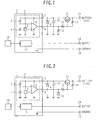
- Fig. 1 illustrates the configuration of an IC power protection circuit according to a first embodiment of the present invention;
- Fig. 2 illustrates the configuration of an IC power protection circuit according to a second embodiment of the present invention;
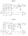
- Fig. 3 illustrates the configuration of an IC power protection circuit according to a third embodiment of the present invention;
- Fig. 4 illustrates the configuration of an IC power protection circuit according to a fourth embodiment of the present invention;
- Fig. 5 illustrates the configuration of an IC power protection circuit according to a fifth embodiment of the present invention; and
- Fig. 6 illustrates the configuration of an IC power protection circuit according to a sixth embodiment of the present invention.
- Embodiments of the present invention will now be described with reference to the accompanying drawings.
- First of all, an IC power protection circuit according to a first embodiment of the present invention will be described below with reference to Fig. 1.
- Referring to Fig. 1, an
error amplification circuit 2, which is a part of the IC power protection circuit, is positioned within an integrated circuit 1 and integrated. The integrated circuit 1 includes a sensorsignal processing circuit 17 that processes a signal output from asensor 16 and outputs the processed sensor output to anoutput terminal 18. - The IC power protection circuit includes a
zener diode 9, which is connected to apower supply terminal 7 of the integrated circuit 1 to prevent an overvoltage from being applied to thepower supply terminal 7, acapacitor 10, which is connected to thepower supply terminal 7 to reduce the power supply impedance of the integrated circuit 1, abattery terminal 15, which receives power from a battery, aground terminal 19; and atransistor 11, which controls a voltage that is supplied from thebattery terminal 15. A collector of thetransistor 11 is connected to thebattery terminal 15 and an emitter of thetransistor 11 is connected to thecapacitor 10. - The IC power protection circuit also includes three
resistors transistor 11 can be controlled by theerror amplification circuit 2. Theresistor 14 is connected between the collector and base of thetransistor 11. Theresistor 13 is connected between the base of thetransistor 11 and an output terminal of the integrated circuit 1. Theresistor 12 is connected between the ground and a connection point between theresistor 13 and anoutput terminal 8. - The
error amplification circuit 2, which is positioned within the integrated circuit 1, is a voltage division section for dividing the supply voltage applied to thepower supply terminal 7 of the integrated circuit 1. It includesresistors power supply terminal 7 and the ground; areference voltage source 5, which generates a reference voltage; and anerror amplifier 6, which amplifies an output difference between thereference voltage source 5 and voltage division section and outputs the amplified output difference to theoutput terminal 8. - A connection point between the
resistors error amplifier 6, and thereference voltage source 5 is connected to the other input terminal of theerror amplifier 6. An output signal generated from theerror amplifier 6 is used to control the transistor to determine whether the transistor is conducting or not so that the voltage supplied from thebattery terminal 15 is adjusted and supplied to the integrated circuit 1. - The power for the
reference voltage source 5 anderror amplifier 6 is supplied from a power source that supplies power to the integrated circuit 1. - In the IC power protection circuit according to the first embodiment of the present invention, the
reference voltage source 5 anderror amplifier 6, which are included in the IC power protection circuit, are positioned in an integrated manner within the integrated circuit 1, and thetransistor 11, which is also included in the IC power protection circuit, is furnished as an element that is separate from the integrated circuit 1. This feature provides the following advantages. - A first advantage of the first embodiment is that the withstand voltage of the
transistor 11 can easily be set to a voltage of 90 V or higher because thetransistor 11 is a stand-alone element. Thus, thetransistor 11 can provide surge protection for thebattery terminal 15, which is required for a vehicle-mounted electronic device. Consequently, no additional surge protection circuit is needed. - If a conventional regulator is used, the withstand voltage of the regulator is limited to 40 V or so because the
reference voltage source 5 anderror amplifier 6 are also integrated within the regulator. Therefore, if a Class A surge (a battery surge having a voltage of 70 V) is applied to the regulator, the regulator breaks down. - In the above case, the use of an additional surge protection circuit is required. If the withstand voltage of the regulator is set to a voltage of 70 V without integrating the regulator, the cost increases considerably.
- A second advantage of the first embodiment is that the
transistor 11 can provide reverse connection protection because it is a stand-alone element. Thus, no additional reverse connection protection circuit is needed. - If a conventional regulator is used, it is configured as an integrated circuit because it includes the
reference voltage source 5 anderror amplifier 6. Therefore, if an inverse voltage is applied to a regulator power source, the regulator breaks down. Thus, it is necessary to furnish a reverse connection protection circuit. - A third advantage of the first embodiment is that the number of parts can be reduced by integrating the
reference voltage source 5 anderror amplifier 6, for instance, within the integrated circuit 1, which includes the sensorsignal processing circuit 17. Thereference voltage source 5 anderror amplifier 6 can be integrated within an integrated circuit having a low withstand voltage. The size is decreased particularly through miniaturization for integration purposes. Therefore, integration within a miniaturizable, low-withstand-voltage integrated circuit is more advantageous than integration within a regulator that requires a high withstand voltage. - To provide the above advantage, a power source for the integrated circuit 1 supplies power to the
reference voltage source 5 anderror amplifier 6. - However, integrating the
error amplifier 6 within a low-withstand-voltage integrated circuit 1 gives rise to some problems. - A first problem relates to reverse connection protection. More specifically, it is demanded that no breakdown occur even when a reverse battery connection is made. In the first embodiment, the
power supply terminal 7 of the integrated circuit 1 is protected by thetransistor 11. However, if theoutput terminal 8 of theerror amplifier 6 is directly connected to the base terminal of thetransistor 11, an overcurrent flows. To avoid such a problem, the first embodiment positions theresistor 13 between theoutput terminal 8 of theerror amplifier 6 and the base terminal of thetransistor 11 and uses it as a reverse connection protection resistor. - A second problem relates to surge protection. In the first embodiment, the
power supply terminal 7 of the integrated circuit 1 is protected by thetransistor 11. However, if theoutput terminal 8 of theerror amplifier 6 is directly connected to the base terminal oftransistor 11, an overcurrent flows. To avoid such a problem, the first embodiment sets up theresistors - The overvoltage
application prevention resistors output terminal 8 of theerror amplifier 6 by resistively dividing the surge voltage applied to thebattery terminal 15. - A third problem relates to startup reliability. If, in the first embodiment, the
transistor 11 is off and unable to supply power to the integrated circuit 1 when the voltage at thebattery terminal 15 changes from 0 V to 14 V, theerror amplifier 6 to which power is supplied from a power source for the integrated circuit 1 may become inoperative, leaving thetransistor 11 off. - The
resistor 14 is positioned as a starting resistor between the base and collector of thetransistor 11 to avoid the above problem. Even if the output generated from theerror amplifier 6 is zero (0) in a situation where the startingresistor 14 is furnished as described above, a certain supply voltage can be applied to the integrated circuit 1 by turning on thetransistor 11. Stable startup is assured by designing thereference voltage source 5 anderror amplifier 6 so that they operate on such a supply voltage. - As described above, the first embodiment of the present invention provides a high withstand voltage by positioning the
error amplifier 6, which is included in the regulator, and thereference voltage source 5 for theerror amplifier 6 in an integrated manner within the integrated circuit 1 to be protected, and by furnishing thevoltage control transistor 11, which is included in the regulator, as a stand-alone element. - Consequently, the present invention provides an IC power protection circuit the cost of which can be reduced while offering the same functions as the surge protection circuit and reverse connection protection circuit.
- An IC power protection circuit according to a second embodiment of the present invention will now be described with reference to Fig. 2.
- The IC power protection circuit according to the second embodiment is obtained by replacing the overvoltage
application prevention resistor 12 according to the first embodiment with azener diode 20. - The second embodiment of the present invention provides the same advantages as the first embodiment. Further, the second embodiment uses the
zener diode 20 to provide battery surge protection for theoutput terminal 8 of theerror amplifier 6. This makes it possible to provide protection against a higher surge voltage. - An IC power protection circuit according to a third embodiment of the present invention will now be described with reference to Fig. 3.
- Referring to Fig. 3, the IC power protection circuit according to the third embodiment is obtained by allowing a
zener diode 21, which is connected between the base of thetransistor 11 and the ground, to perform the functions of thezener diode 9 andresistor 12 in the first embodiment, and removing thezener diode 9 andresistor 12 from the configuration. - The third embodiment provides the same advantages as the first embodiment. However, the
zener diode 21 provides overvoltage protection for the power source of the integrated circuit 1 and for the output terminal of theerror amplifier 6. This makes it possible to reduce the number of parts. - In the third embodiment, the
zener diode 21 limits the base voltage of thetransistor 11 to limit the emitter voltage of thetransistor 11, thereby providing overvoltage protection for the integrated circuit 1. - The
zener diode 21 also provides overvoltage protection for theoutput terminal 8 of theerror amplifier 6 by limiting the voltage. - An IC power protection circuit according to a fourth embodiment of the present invention will now be described with reference to Fig. 4.
- The IC power protection circuit according to the fourth embodiment is obtained by replacing the
reference voltage source 5 in theerror amplification circuit 2 for the integrated circuit according to the third embodiment with aresistor 22 andzener diode 23 that are positioned outside the integrated circuit 1. - More specifically, the
resistor 22 andzener diode 23 are serially connected between thepower supply terminal 7 and the ground. A connection point between theresistor 22 andzener diode 23 is connected to an input terminal of theerror amplifier 6. Thereference voltage source 5 is removed from the configuration. - The fourth embodiment provides the same advantages as the first embodiment. In the fourth embodiment, the
reference voltage source 5 is replaced with external elements so that the present invention can be implemented even when the integrated circuit 1 is a CMOS LSI. - The CMOS LSI can be miniaturized to a great extent; however, it is difficult to integrate the
reference voltage source 5. Therefore, the reference voltage source is composed of external elements (resistor 22 and zener diode 23). - An IC power protection circuit according to a fifth embodiment of the present invent'ion will now be described with reference to Fig. 5.
- The IC power protection circuit according to the fifth embodiment is obtained by replacing the
zener diode 21 in the fourth embodiment withdiodes zener diode 23 doubles as a reference voltage source). - More specifically, an anode of the
diode 25 is connected to a connection point between theresistor 14 and the base of thetransistor 11, and a cathode of thediode 25 is connected to an anode of thediode 24. - A cathode of the
diode 24 is connected to a cathode of thezener diode 23, and an anode of thezener diode 23 is connected to the ground. - In the fifth embodiment, the
zener diode 23, which is used for reference voltage generation, and thediodes transistor 11. This provides overvoltage protection for thepower supply terminal 7 of the integrated circuit 1 and for theoutput terminal 8 of theerror amplifier 6. - The fifth embodiment provides the same advantages as the fourth embodiment. In addition, the cost of parts can be reduced because the
zener diode 21 in the fourth embodiment is replaced with thediodes - An IC power protection circuit according to a sixth embodiment of the present invention will now be described with reference to Fig. 6.
- The IC power protection circuit according to the sixth embodiment has the same basic configuration as the power supply circuit for the integrated circuit in the third embodiment except that an external sensor voltage supply section is added. The external sensor voltage supply section includes a
transistor 26,resistors zener diode 29. - More specifically, the
battery terminal 15 is connected to thesensor 16 via a collector and emitter of thetransistor 26. The collector of thetransistor 26 is connected to the ground via theresistor 28 andzener diode 29. A connection point between theresistor 28 andzener diode 29 is connected not only to a base of thetransistor 26 but also to a sensorsignal processing circuit 30 via theresistor 27. - Since the employed configuration is as described above, the sensor
signal processing circuit 30 can cause thebattery terminal 15 to apply a voltage to thesensor 16. The voltage applied to thesensor 16 can be higher than the withstand voltage of the integrated circuit 1. - In other words, the sensor
signal processing circuit 30 can control thetransistor 26 so that a voltage is directly supplied from thebattery terminal 15 to an airflow sensor orother sensor 16 that requires a high voltage and large current. - As is the case with the
output terminal 8 of theerror amplifier 6, which was explained earlier, theresistor 27 andzener diode 29 provide overvoltage protection and reverse connection protection for a voltage output terminal (the output terminal of the integrated circuit 1) that delivers an output to the base of thetransistor 26 from the sensorsignal processing circuit 30 for control purposes. - The sixth embodiment provides the same advantages as the third embodiment. In addition, the sensor
signal processing circuit 30 can control thetransistor 26, as described earlier, so that a voltage is directly supplied from thebattery terminal 15 to thesensor 16. - The sixth embodiment assumes that the
reference voltage source 5 is positioned inside the integrated circuit 1, and allows the sensorsignal processing circuit 30 to control thetransistor 26 so that a voltage is directly supplied from thebattery terminal 15 to thesensor 16. However, the present invention can also be applied to a case where thereference voltage source 5 is positioned outside the integrated circuit 1 as indicated by the examples shown in Figs. 4 and 5.
Claims (12)
- An IC power protection circuit which supplies power to an integrated circuit whose withstand voltage is lower than a supply voltage supplied from the outside, the IC power protection circuit comprising:an error amplification circuit which is positioned in an integrated manner within the integrated circuit, and includes a voltage division section for dividing a voltage applied to a power supply terminal of the integrated circuit and an error amplifier for amplifying a difference between an output from the voltage division section and a reference voltage;a voltage control transistor which conducts depending on an output from the error amplifier, adjusts a voltage supplied from an external power source, and supplies the adjusted voltage to the integrated circuit; andan output terminal protection voltage limiting section which limits the voltage applied to an output terminal of the error amplifier to a voltage not higher than the withstand voltage of the integrated circuit.
- The IC power protection circuit according to claim 1, wherein a reference voltage source generating the reference voltage is positioned in an integrated manner within the integrated circuit.
- The IC power protection circuit according to claim 1, wherein said output terminal protection voltage limiting section is composed of a plurality of resistive elements.
- The IC power protection circuit according to claim 1, wherein said output terminal protection voltage limiting section is a zener diode.
- The IC power protection circuit according to claim 1, further comprising an input terminal protection voltage limiting section which limits the voltage applied to an input terminal of the integrated circuit to a voltage not higher than the withstand voltage of the integrated circuit.
- The IC power protection circuit according to claim 1, further comprising a base voltage limiting section which limits the voltage applied to a base terminal of said voltage control transistor to a voltage not higher than the withstand voltage of the integrated circuit.
- The IC power protection circuit according to claim 5, wherein the base voltage limiting section is a zener diode.
- The IC power protection circuit according to claim 1, wherein a sensor signal processing circuit is integrated within the integrated circuit to receive a signal supplied from an external sensor, process the received signal, and transfers the processed signal out of the integrated circuit.
- The IC power protection circuit according to claim 8, further comprising an external sensor voltage supply section which controls a supply voltage supplied from the outside in accordance with a control signal from the sensor signal processing circuit and supplies the controlled supply voltage to the external sensor.
- The IC power protection circuit according to claim 1, wherein a starting resistor is connected between a collector and a base of said voltage control transistor.
- The IC power protection circuit according to claim 1, wherein a reference voltage source generating the reference voltage is positioned outside the integrated circuit.
- The IC power protection circuit according to claim 11, wherein the reference voltage source generating the reference voltage is composed of a resistor which is connected to the power supply terminal of the integrated circuit and a zener diode which is connected in series with the resistor.
Applications Claiming Priority (1)
| Application Number | Priority Date | Filing Date | Title |
|---|---|---|---|
| JP2006065654A JP4690915B2 (en) | 2006-03-10 | 2006-03-10 | Integrated circuit power protection circuit |
Publications (2)
| Publication Number | Publication Date |
|---|---|
| EP1833136A1 true EP1833136A1 (en) | 2007-09-12 |
| EP1833136B1 EP1833136B1 (en) | 2010-05-26 |
Family
ID=38267951
Family Applications (1)
| Application Number | Title | Priority Date | Filing Date |
|---|---|---|---|
| EP07001770A Ceased EP1833136B1 (en) | 2006-03-10 | 2007-01-26 | Ic power protection circuit |
Country Status (5)
| Country | Link |
|---|---|
| US (1) | US7656624B2 (en) |
| EP (1) | EP1833136B1 (en) |
| JP (1) | JP4690915B2 (en) |
| CN (1) | CN101034805B (en) |
| DE (1) | DE602007006702D1 (en) |
Cited By (1)
| Publication number | Priority date | Publication date | Assignee | Title |
|---|---|---|---|---|
| ES2342645A1 (en) * | 2008-05-14 | 2010-07-09 | Farsens, S.L. | Tension limiting circuit. (Machine-translation by Google Translate, not legally binding) |
Families Citing this family (11)
| Publication number | Priority date | Publication date | Assignee | Title |
|---|---|---|---|---|
| DE102005011520A1 (en) * | 2005-03-10 | 2006-10-05 | Danfoss Compressors Gmbh | Apparatus and method for providing a DC voltage |
| US20080239603A1 (en) * | 2007-03-27 | 2008-10-02 | Eaglepicher Energy Products Corporation | Battery protection circuit for lithium cabon monofluoride battery |
| JP5513778B2 (en) * | 2008-08-18 | 2014-06-04 | パナソニック株式会社 | Switching power supply circuit |
| JP5287561B2 (en) * | 2009-07-10 | 2013-09-11 | パナソニック株式会社 | Stabilized power circuit |
| CN102201664A (en) * | 2010-03-25 | 2011-09-28 | 鸿富锦精密工业(深圳)有限公司 | Voltage-stabilizing circuit system |
| CN104184103B (en) * | 2013-05-27 | 2017-09-22 | 深圳市海洋王照明工程有限公司 | A kind of output overcurrent protection circuit |
| CN103346546A (en) * | 2013-06-28 | 2013-10-09 | 成都汉康信息产业有限公司 | Lightning protection circuit used for remote measurement terminal |
| JP6229040B2 (en) * | 2014-03-06 | 2017-11-08 | アルプス電気株式会社 | Semiconductor integrated circuit device and sensing module having the same |
| JP6270549B2 (en) * | 2014-03-06 | 2018-01-31 | 株式会社 日立パワーデバイス | Semiconductor device, motor using the same, and air conditioner |
| CN104270410A (en) * | 2014-09-05 | 2015-01-07 | 重庆市汇链信息科技有限公司 | Digital recording and processing device for mass data of audio and video |
| JP6581443B2 (en) * | 2015-09-04 | 2019-09-25 | 日立オートモティブシステムズ株式会社 | Sensor device |
Citations (5)
| Publication number | Priority date | Publication date | Assignee | Title |
|---|---|---|---|---|
| DE19605628C1 (en) * | 1995-11-28 | 1997-05-28 | Lg Semicon Co Ltd | Circuit for avoiding electrostatic discharge and latch-up |
| FR2782581A1 (en) * | 1998-08-18 | 2000-02-25 | St Microelectronics Sa | Protection against electrostatic discharges for integrated circuits used in radio-frequency applications |
| WO2002029950A2 (en) | 2000-10-06 | 2002-04-11 | Qualcomm Incorporated | Electro-static discharge protection circuit |
| US20040150930A1 (en) | 2003-01-21 | 2004-08-05 | Rohm Co., Ltd. | Electronic apparatus |
| JP2005083221A (en) | 2003-09-05 | 2005-03-31 | Mitsubishi Electric Corp | Power circuit of on-vehicle electronic controller |
Family Cites Families (11)
| Publication number | Priority date | Publication date | Assignee | Title |
|---|---|---|---|---|
| US4008418A (en) * | 1976-03-02 | 1977-02-15 | Fairchild Camera And Instrument Corporation | High voltage transient protection circuit for voltage regulators |
| DE2638178C2 (en) * | 1976-08-25 | 1986-01-02 | Robert Bosch Gmbh, 7000 Stuttgart | Protection device for integrated circuits against overvoltages |
| JPS6336405Y2 (en) * | 1980-04-18 | 1988-09-27 | ||
| JPS56156110A (en) | 1980-05-01 | 1981-12-02 | Kongo Kk | Safety apparatus of movable shelf |
| JPH07147727A (en) * | 1993-11-24 | 1995-06-06 | Nippondenso Co Ltd | Surge voltage protective circuit |
| JP3147145B2 (en) * | 1996-08-30 | 2001-03-19 | 日本電気株式会社 | Power supply circuit for low voltage IC |
| JP2000112542A (en) * | 1998-10-01 | 2000-04-21 | Mitsubishi Electric Corp | Constant voltage circuit |
| JP3642699B2 (en) * | 1999-05-10 | 2005-04-27 | シャープ株式会社 | DC stabilized power circuit protection circuit |
| JP2001012542A (en) | 1999-06-24 | 2001-01-16 | Daido Metal Co Ltd | Supporting device for base isolation |
| JP2001337729A (en) * | 2000-05-29 | 2001-12-07 | Fujitsu Ten Ltd | Series regulator |
| JP2004208449A (en) * | 2002-12-26 | 2004-07-22 | Hitachi Ltd | Electronic equipment control device |
-
2006
- 2006-03-10 JP JP2006065654A patent/JP4690915B2/en not_active Expired - Fee Related
- 2006-12-28 CN CN2006101720931A patent/CN101034805B/en not_active Expired - Fee Related
-
2007
- 2007-01-24 US US11/656,994 patent/US7656624B2/en not_active Expired - Fee Related
- 2007-01-26 DE DE602007006702T patent/DE602007006702D1/en active Active
- 2007-01-26 EP EP07001770A patent/EP1833136B1/en not_active Ceased
Patent Citations (5)
| Publication number | Priority date | Publication date | Assignee | Title |
|---|---|---|---|---|
| DE19605628C1 (en) * | 1995-11-28 | 1997-05-28 | Lg Semicon Co Ltd | Circuit for avoiding electrostatic discharge and latch-up |
| FR2782581A1 (en) * | 1998-08-18 | 2000-02-25 | St Microelectronics Sa | Protection against electrostatic discharges for integrated circuits used in radio-frequency applications |
| WO2002029950A2 (en) | 2000-10-06 | 2002-04-11 | Qualcomm Incorporated | Electro-static discharge protection circuit |
| US20040150930A1 (en) | 2003-01-21 | 2004-08-05 | Rohm Co., Ltd. | Electronic apparatus |
| JP2005083221A (en) | 2003-09-05 | 2005-03-31 | Mitsubishi Electric Corp | Power circuit of on-vehicle electronic controller |
Cited By (2)
| Publication number | Priority date | Publication date | Assignee | Title |
|---|---|---|---|---|
| ES2342645A1 (en) * | 2008-05-14 | 2010-07-09 | Farsens, S.L. | Tension limiting circuit. (Machine-translation by Google Translate, not legally binding) |
| ES2342645B1 (en) * | 2008-05-14 | 2011-04-26 | Farsens, S.L. | VOLTAGE LIMITING CIRCUIT. |
Also Published As
| Publication number | Publication date |
|---|---|
| CN101034805B (en) | 2012-11-14 |
| US20070211394A1 (en) | 2007-09-13 |
| EP1833136B1 (en) | 2010-05-26 |
| DE602007006702D1 (en) | 2010-07-08 |
| CN101034805A (en) | 2007-09-12 |
| US7656624B2 (en) | 2010-02-02 |
| JP4690915B2 (en) | 2011-06-01 |
| JP2007244147A (en) | 2007-09-20 |
Similar Documents
| Publication | Publication Date | Title |
|---|---|---|
| US7656624B2 (en) | IC power protection circuit | |
| US7859325B2 (en) | CPU core voltage supply circuit | |
| US8508900B2 (en) | Overvoltage protection circuit and electronic device comprising the same | |
| US20080203982A1 (en) | Power supply system for motherboard | |
| US12013421B2 (en) | Electronic circuit and sensor system | |
| US7791494B2 (en) | Voltage monitoring device | |
| US20100045117A1 (en) | Protection device for a power source and power unit using same | |
| TW201908905A (en) | Switching controller and method for load | |
| KR100778203B1 (en) | Power supply protection circuit for an in-vehicle eletronic device | |
| US20130003236A1 (en) | Power supply circuit | |
| US7408396B2 (en) | High voltage protection circuit | |
| US7924543B2 (en) | Current-limiting circuit with additional current path | |
| JP3848265B2 (en) | Electronic equipment | |
| US8222960B2 (en) | RF power amplifier | |
| US20070096786A1 (en) | Reset circuit | |
| US12109958B2 (en) | In-vehicle semiconductor circuit and semiconductor circuit | |
| US7436157B2 (en) | Device for preparing a supply voltage | |
| US9240683B2 (en) | Over-current regulating system | |
| JP2010220390A (en) | Overvoltage protective circuit | |
| CN112566343B (en) | No-load protection circuit | |
| KR100934249B1 (en) | Current limiting circuit | |
| JP2005242769A (en) | Power supply reset circuit and regulator ic with built-in power supply reset circuit | |
| JP2007156641A (en) | Power supply circuit | |
| KR101228924B1 (en) | VCC circuit of inverter for LCD Backlight | |
| US20100315156A1 (en) | Volatage bandgap reference circuit |
Legal Events
| Date | Code | Title | Description |
|---|---|---|---|
| PUAI | Public reference made under article 153(3) epc to a published international application that has entered the european phase |
Free format text: ORIGINAL CODE: 0009012 |
|
| AK | Designated contracting states |
Kind code of ref document: A1 Designated state(s): AT BE BG CH CY CZ DE DK EE ES FI FR GB GR HU IE IS IT LI LT LU LV MC NL PL PT RO SE SI SK TR |
|
| AX | Request for extension of the european patent |
Extension state: AL BA HR MK YU |
|
| RIN1 | Information on inventor provided before grant (corrected) |
Inventor name: NAKANO, HIROSHI, C/O HITACHI, LTD., INT. PROP. Inventor name: YAMADA, MASAMICHI, C/O HITACHI, LTD., INT. PROP. Inventor name: MATSUMOTO, MASAHIRO, C/O HITACHI, LTD., INT. PROP. Inventor name: HANZAWA KEIJI, C/O HITACHI CAR ENG.CO.LTD. Inventor name: SATO, RYO, C/O HITACHI, LTD., INT. PROP. |
|
| RIN1 | Information on inventor provided before grant (corrected) |
Inventor name: MATSUMOTO, MASAHIROC/O HITACHI, LTD., INTELLECTUAL Inventor name: NAKANO, HIROSHIC/O HITACHI, LTD., INTELLECTUAL PRO Inventor name: HANZAWA KEIJIC/O HITACHI CAR ENGINEERING CO., LTD. Inventor name: SATO, RYOC/O HITACHI, LTD., INTELLECTUAL PROPERTY Inventor name: YAMADA, MASAMICHIC/O HITACHI, LTD., INTELLECTUAL P |
|
| 17P | Request for examination filed |
Effective date: 20080312 |
|
| 17Q | First examination report despatched |
Effective date: 20080410 |
|
| AKX | Designation fees paid |
Designated state(s): DE |
|
| GRAP | Despatch of communication of intention to grant a patent |
Free format text: ORIGINAL CODE: EPIDOSNIGR1 |
|
| GRAS | Grant fee paid |
Free format text: ORIGINAL CODE: EPIDOSNIGR3 |
|
| GRAA | (expected) grant |
Free format text: ORIGINAL CODE: 0009210 |
|
| AK | Designated contracting states |
Kind code of ref document: B1 Designated state(s): DE |
|
| REF | Corresponds to: |
Ref document number: 602007006702 Country of ref document: DE Date of ref document: 20100708 Kind code of ref document: P |
|
| PLBE | No opposition filed within time limit |
Free format text: ORIGINAL CODE: 0009261 |
|
| STAA | Information on the status of an ep patent application or granted ep patent |
Free format text: STATUS: NO OPPOSITION FILED WITHIN TIME LIMIT |
|
| 26N | No opposition filed |
Effective date: 20110301 |
|
| REG | Reference to a national code |
Ref country code: DE Ref legal event code: R097 Ref document number: 602007006702 Country of ref document: DE Effective date: 20110228 |
|
| REG | Reference to a national code |
Ref country code: DE Ref legal event code: R409 Ref document number: 602007006702 Country of ref document: DE |
|
| REG | Reference to a national code |
Ref country code: DE Ref legal event code: R119 Ref document number: 602007006702 Country of ref document: DE Effective date: 20110802 |
|
| REG | Reference to a national code |
Ref country code: DE Ref legal event code: R409 Ref document number: 602007006702 Country of ref document: DE |
|
| REG | Reference to a national code |
Ref country code: DE Ref legal event code: R409 Ref document number: 602007006702 Country of ref document: DE |
|
| REG | Reference to a national code |
Ref country code: DE Ref legal event code: R081 Ref document number: 602007006702 Country of ref document: DE Owner name: HITACHI ASTEMO, LTD., HITACHINAKA-SHI, JP Free format text: FORMER OWNER: HITACHI AUTOMOTIVE SYSTEMS, LTD., HITACHINAKA-SHI, IBARAKI, JP Ref country code: DE Ref legal event code: R081 Ref document number: 602007006702 Country of ref document: DE Owner name: HITACHI ASTEMO, LTD., HITACHINAKA-SHI, JP Free format text: FORMER OWNER: HITACHI, LTD., TOKYO, JP |
|
| PGFP | Annual fee paid to national office [announced via postgrant information from national office to epo] |
Ref country code: DE Payment date: 20221130 Year of fee payment: 17 |
|
| REG | Reference to a national code |
Ref country code: DE Ref legal event code: R119 Ref document number: 602007006702 Country of ref document: DE |
|
| PG25 | Lapsed in a contracting state [announced via postgrant information from national office to epo] |
Ref country code: DE Free format text: LAPSE BECAUSE OF NON-PAYMENT OF DUE FEES Effective date: 20240801 |
|
| PG25 | Lapsed in a contracting state [announced via postgrant information from national office to epo] |
Ref country code: DE Free format text: LAPSE BECAUSE OF NON-PAYMENT OF DUE FEES Effective date: 20240801 |