EP1833128B1 - Optical semiconductor device with diffraction grating - Google Patents
Optical semiconductor device with diffraction grating Download PDFInfo
- Publication number
- EP1833128B1 EP1833128B1 EP07103717A EP07103717A EP1833128B1 EP 1833128 B1 EP1833128 B1 EP 1833128B1 EP 07103717 A EP07103717 A EP 07103717A EP 07103717 A EP07103717 A EP 07103717A EP 1833128 B1 EP1833128 B1 EP 1833128B1
- Authority
- EP
- European Patent Office
- Prior art keywords
- diffraction grating
- semiconductor device
- optical semiconductor
- waveguide
- width
- Prior art date
- Legal status (The legal status is an assumption and is not a legal conclusion. Google has not performed a legal analysis and makes no representation as to the accuracy of the status listed.)
- Not-in-force
Links
Images



Classifications
-
- H—ELECTRICITY
- H01—ELECTRIC ELEMENTS
- H01S—DEVICES USING THE PROCESS OF LIGHT AMPLIFICATION BY STIMULATED EMISSION OF RADIATION [LASER] TO AMPLIFY OR GENERATE LIGHT; DEVICES USING STIMULATED EMISSION OF ELECTROMAGNETIC RADIATION IN WAVE RANGES OTHER THAN OPTICAL
- H01S5/00—Semiconductor lasers
- H01S5/10—Construction or shape of the optical resonator, e.g. extended or external cavity, coupled cavities, bent-guide, varying width, thickness or composition of the active region
- H01S5/12—Construction or shape of the optical resonator, e.g. extended or external cavity, coupled cavities, bent-guide, varying width, thickness or composition of the active region the resonator having a periodic structure, e.g. in distributed feedback [DFB] lasers
-
- B—PERFORMING OPERATIONS; TRANSPORTING
- B82—NANOTECHNOLOGY
- B82Y—SPECIFIC USES OR APPLICATIONS OF NANOSTRUCTURES; MEASUREMENT OR ANALYSIS OF NANOSTRUCTURES; MANUFACTURE OR TREATMENT OF NANOSTRUCTURES
- B82Y20/00—Nanooptics, e.g. quantum optics or photonic crystals
-
- H—ELECTRICITY
- H01—ELECTRIC ELEMENTS
- H01S—DEVICES USING THE PROCESS OF LIGHT AMPLIFICATION BY STIMULATED EMISSION OF RADIATION [LASER] TO AMPLIFY OR GENERATE LIGHT; DEVICES USING STIMULATED EMISSION OF ELECTROMAGNETIC RADIATION IN WAVE RANGES OTHER THAN OPTICAL
- H01S5/00—Semiconductor lasers
- H01S5/06—Arrangements for controlling the laser output parameters, e.g. by operating on the active medium
- H01S5/065—Mode locking; Mode suppression; Mode selection ; Self pulsating
- H01S5/0651—Mode control
- H01S5/0653—Mode suppression, e.g. specific multimode
- H01S5/0655—Single transverse or lateral mode emission
-
- H—ELECTRICITY
- H01—ELECTRIC ELEMENTS
- H01S—DEVICES USING THE PROCESS OF LIGHT AMPLIFICATION BY STIMULATED EMISSION OF RADIATION [LASER] TO AMPLIFY OR GENERATE LIGHT; DEVICES USING STIMULATED EMISSION OF ELECTROMAGNETIC RADIATION IN WAVE RANGES OTHER THAN OPTICAL
- H01S5/00—Semiconductor lasers
- H01S5/10—Construction or shape of the optical resonator, e.g. extended or external cavity, coupled cavities, bent-guide, varying width, thickness or composition of the active region
- H01S5/1053—Comprising an active region having a varying composition or cross-section in a specific direction
- H01S5/1064—Comprising an active region having a varying composition or cross-section in a specific direction varying width along the optical axis
-
- H—ELECTRICITY
- H01—ELECTRIC ELEMENTS
- H01S—DEVICES USING THE PROCESS OF LIGHT AMPLIFICATION BY STIMULATED EMISSION OF RADIATION [LASER] TO AMPLIFY OR GENERATE LIGHT; DEVICES USING STIMULATED EMISSION OF ELECTROMAGNETIC RADIATION IN WAVE RANGES OTHER THAN OPTICAL
- H01S5/00—Semiconductor lasers
- H01S5/10—Construction or shape of the optical resonator, e.g. extended or external cavity, coupled cavities, bent-guide, varying width, thickness or composition of the active region
- H01S5/12—Construction or shape of the optical resonator, e.g. extended or external cavity, coupled cavities, bent-guide, varying width, thickness or composition of the active region the resonator having a periodic structure, e.g. in distributed feedback [DFB] lasers
- H01S5/1206—Construction or shape of the optical resonator, e.g. extended or external cavity, coupled cavities, bent-guide, varying width, thickness or composition of the active region the resonator having a periodic structure, e.g. in distributed feedback [DFB] lasers having a non constant or multiplicity of periods
- H01S5/1212—Chirped grating
-
- H—ELECTRICITY
- H01—ELECTRIC ELEMENTS
- H01S—DEVICES USING THE PROCESS OF LIGHT AMPLIFICATION BY STIMULATED EMISSION OF RADIATION [LASER] TO AMPLIFY OR GENERATE LIGHT; DEVICES USING STIMULATED EMISSION OF ELECTROMAGNETIC RADIATION IN WAVE RANGES OTHER THAN OPTICAL
- H01S5/00—Semiconductor lasers
- H01S5/10—Construction or shape of the optical resonator, e.g. extended or external cavity, coupled cavities, bent-guide, varying width, thickness or composition of the active region
- H01S5/12—Construction or shape of the optical resonator, e.g. extended or external cavity, coupled cavities, bent-guide, varying width, thickness or composition of the active region the resonator having a periodic structure, e.g. in distributed feedback [DFB] lasers
- H01S5/1225—Construction or shape of the optical resonator, e.g. extended or external cavity, coupled cavities, bent-guide, varying width, thickness or composition of the active region the resonator having a periodic structure, e.g. in distributed feedback [DFB] lasers with a varying coupling constant along the optical axis
-
- H—ELECTRICITY
- H01—ELECTRIC ELEMENTS
- H01S—DEVICES USING THE PROCESS OF LIGHT AMPLIFICATION BY STIMULATED EMISSION OF RADIATION [LASER] TO AMPLIFY OR GENERATE LIGHT; DEVICES USING STIMULATED EMISSION OF ELECTROMAGNETIC RADIATION IN WAVE RANGES OTHER THAN OPTICAL
- H01S5/00—Semiconductor lasers
- H01S5/10—Construction or shape of the optical resonator, e.g. extended or external cavity, coupled cavities, bent-guide, varying width, thickness or composition of the active region
- H01S5/12—Construction or shape of the optical resonator, e.g. extended or external cavity, coupled cavities, bent-guide, varying width, thickness or composition of the active region the resonator having a periodic structure, e.g. in distributed feedback [DFB] lasers
- H01S5/1237—Lateral grating, i.e. grating only adjacent ridge or mesa
-
- H—ELECTRICITY
- H01—ELECTRIC ELEMENTS
- H01S—DEVICES USING THE PROCESS OF LIGHT AMPLIFICATION BY STIMULATED EMISSION OF RADIATION [LASER] TO AMPLIFY OR GENERATE LIGHT; DEVICES USING STIMULATED EMISSION OF ELECTROMAGNETIC RADIATION IN WAVE RANGES OTHER THAN OPTICAL
- H01S5/00—Semiconductor lasers
- H01S5/20—Structure or shape of the semiconductor body to guide the optical wave ; Confining structures perpendicular to the optical axis, e.g. index or gain guiding, stripe geometry, broad area lasers, gain tailoring, transverse or lateral reflectors, special cladding structures, MQW barrier reflection layers
- H01S5/22—Structure or shape of the semiconductor body to guide the optical wave ; Confining structures perpendicular to the optical axis, e.g. index or gain guiding, stripe geometry, broad area lasers, gain tailoring, transverse or lateral reflectors, special cladding structures, MQW barrier reflection layers having a ridge or stripe structure
-
- H—ELECTRICITY
- H01—ELECTRIC ELEMENTS
- H01S—DEVICES USING THE PROCESS OF LIGHT AMPLIFICATION BY STIMULATED EMISSION OF RADIATION [LASER] TO AMPLIFY OR GENERATE LIGHT; DEVICES USING STIMULATED EMISSION OF ELECTROMAGNETIC RADIATION IN WAVE RANGES OTHER THAN OPTICAL
- H01S5/00—Semiconductor lasers
- H01S5/30—Structure or shape of the active region; Materials used for the active region
- H01S5/34—Structure or shape of the active region; Materials used for the active region comprising quantum well or superlattice structures, e.g. single quantum well [SQW] lasers, multiple quantum well [MQW] lasers or graded index separate confinement heterostructure [GRINSCH] lasers
- H01S5/341—Structures having reduced dimensionality, e.g. quantum wires
- H01S5/3412—Structures having reduced dimensionality, e.g. quantum wires quantum box or quantum dash
-
- H—ELECTRICITY
- H01—ELECTRIC ELEMENTS
- H01S—DEVICES USING THE PROCESS OF LIGHT AMPLIFICATION BY STIMULATED EMISSION OF RADIATION [LASER] TO AMPLIFY OR GENERATE LIGHT; DEVICES USING STIMULATED EMISSION OF ELECTROMAGNETIC RADIATION IN WAVE RANGES OTHER THAN OPTICAL
- H01S5/00—Semiconductor lasers
- H01S5/30—Structure or shape of the active region; Materials used for the active region
- H01S5/34—Structure or shape of the active region; Materials used for the active region comprising quantum well or superlattice structures, e.g. single quantum well [SQW] lasers, multiple quantum well [MQW] lasers or graded index separate confinement heterostructure [GRINSCH] lasers
- H01S5/343—Structure or shape of the active region; Materials used for the active region comprising quantum well or superlattice structures, e.g. single quantum well [SQW] lasers, multiple quantum well [MQW] lasers or graded index separate confinement heterostructure [GRINSCH] lasers in AIIIBV compounds, e.g. AlGaAs-laser, InP-based laser
- H01S5/34306—Structure or shape of the active region; Materials used for the active region comprising quantum well or superlattice structures, e.g. single quantum well [SQW] lasers, multiple quantum well [MQW] lasers or graded index separate confinement heterostructure [GRINSCH] lasers in AIIIBV compounds, e.g. AlGaAs-laser, InP-based laser emitting light at a wavelength longer than 1000nm, e.g. InP based 1300 and 1500nm lasers
Definitions
- the present invention relates to an optical semiconductor device having a diffraction grating, and more particularly to an optical semiconductor device having a vertical groove diffraction grating.
- the following methods are known as a method of forming a diffraction grating of a distributed feedback (DFB) laser or a distributed Bragg reflector (DBR) laser: (1) a regrowth method by which a diffraction grating pattern is formed on the surface of a lower growth layer, and an upper crystal growth layer is regrown on the lower growth layer to form a diffraction grating at the interface of the growth layer; and (2) collective etching method by which a diffraction grating is formed by etching vertical grooves periodically disposed along a waveguide direction on the sidewalls of a waveguide structure, etching starting from the surface of epitaxial stack structure.
- DBR distributed Bragg reflector
- the regrowth method (1) it is necessary for the regrowth method (1) to perform crystal growth twice, which is likely to increase cost. If the surface of the lower growth layer is made of material which contains Al, the regrowth itself may be difficult. For applications requiring low cost, the collective etching method (2) is preferable in many cases.
- the collective etching method (2) is a simple manufacturing method which can form at the same time both a waveguide structure and a diffraction grating by deeply etching a stacked layer structure.
- the width of the waveguide is narrowed beyond a certain point, a higher order transverse mode becomes likely to oscillate, forming two or more optical intensity peaks along a waveguide width direction.
- the device resistance increases.
- JP-A-2003-152273 proposes to suppress a higher order transverse mode by causing a loss by covering a diffraction grating with an absorbing material such as GaAs. This method results in a loss also in the fundamental mode, being likely to raise a threshold value and lower an efficiency.
- JP-A-2001-133647 proposes to eliminate a higher order mode by forming a diffraction grating on sidewalls of a waveguide structure at a pitch longer than ⁇ /2 and shorter than ⁇ , where ⁇ is a waveguide effective wavelength.
- This diffraction grating has a function different from the diffraction grating of a DFB laser or DBR laser.
- EP 0632299 discloses that in the longitudinal direction (z direction, axial direction) a sequence of grating-free partial regions are formed, which are bordered laterally by two DFB or DBR grating regions. These grating regions are in turn bounded laterally on the outside by grating-free partial regions.
- the four lateral grating limits are designed in the shape of continuously running curves.
- US 2002/0141467 discloses a semiconductor laser device in which a n-InP cladding layer, SCH-MQW active layer, p-InP cladding layer, and p-GaInAsP optical waveguide layer are respectively formed into a tapered shape on the n-InP substrate.
- WO 2005/060058 discloses a semiconductor laser having an active waveguide composed of a 1x1-MMI waveguide region and single-mode waveguide regions connected to both ends of the 1x1-MMI waveguide region.
- a grating for selecting a single wavelength of the oscillated light propagated through the active waveguide is provided to the single-mode waveguide region.
- US 4,783,788 discloses a wide stripe double heterostructure laser, which utilizes the mode dependent coupling loss which occurs when a laterally wide wave-guided active region is formed longitudinally adjacent and contiguous with a laterally narrow wave-guided active region.
- the wide wave-guided region is normally wide enough to support higher order lateral modes while the narrow wave-guided region can support only the fundamental lateral mode.
- An embodiment of the present invention may provide an optical semiconductor device capable of suppressing generation of a higher order transverse mode, the optical semiconductor device having a vertical groove diffraction grating on sidewalls of a waveguide.
- the optical semiconductor device may also be capable of suppressing an increase in a device resistance.
- an optical semiconductor device comprising: a waveguide structure defining a propagation direction and having a width defined by sidewalls of the waveguide structure, and including a wide portion, a narrow portion, and an intermediate portion connecting said wide portion and said narrow portion, formed along a propagation direction; and a diffraction grating formed on the sidewalls of at least one of said wide portion and said narrow portion of said waveguide structure, said diffraction grating having vertical grooves periodically disposed along the propagation direction and defining a wavelength of propagation light, and characterized in that the wide portion has a constant first width and a first length, the narrow portion has a constant second width and a second length and is narrower than said wide portion, and the intermediate portion has a width that changes gradually and linearly from the first width to the second width, wherein said narrow portion has a second width and a length such that a loss of 50 % or more is given to a higher order transverse mode.
- the narrow width portion suppresses the higher order transverse mode and the wide width portion suppresses an increase in a device resistance.
- Fig. 1A shows a ridge type laser according to the first embodiment of the present invention.
- Formed on an n-type (001) GaAs substrate 1 by molecular beam epitaxy (MBE) are: an n-type Al 0.4 Ga 0.6 As clad layer 2 having a thickness of 1.4 ⁇ m; an active layer 3 including multiple quantum dot layers; a p-type Al 0.4 Ga 0.6 As clad layer 4 having a thickness of 1.4 ⁇ m; and a p-type GaAs contact layer 5 having a thickness of 0.4 ⁇ m.
- MBE molecular beam epitaxy
- the active layer 3 having ten quantum dot layers is formed by the following processes. After a GaAs barrier layer 3b having a thickness of, e.g., 36 nm is grown, InAs having a large lattice mismatch is grown in molecular layer order to form an InAs quantum dot layer 3qd by a self formation method in Stranski-Krastanov growth mode (S-K mode) which forms quantum dots at a thickness larger than a critical thickness. This InAs quantum dot layer is covered with a GaAs barrier layer 3b having a thickness of 36 nm.
- S-K mode Stranski-Krastanov growth mode
- pairs of similar InAs quantum dot layer 3qd and GaAs barrier layer 3b having the thickness of 36 nm are grown nine times.
- a quantum dot layer for example, refer to paragraphs [0013] to [0070] of published Japanese Patent No. 3672678 (corresponding to US Patent No. 3,672,527 ).
- An InGaAs cap layer 3c may be formed on the GaAs barrier layer 3b to adjust an oscillation wavelength.
- a silicon oxide layer having a thickness of, e.g., 300 nm is formed on the semiconductor layer structure by chemical vapor deposition (CVD) or the like, and an electron beam resist film is coated on the silicon oxide layer.
- CVD chemical vapor deposition
- a pattern of a ridge waveguide and a diffraction grating is exposed in the electron beam resist film, and is developed to form the electron beam resist pattern.
- the resist pattern is transferred to the silicon oxide layer to form a hard mask.
- a propagation direction of the waveguide is referred to below as the length direction, and the transverse direction as the width direction.
- a mask pattern MP has a diffraction grating portion DG on both sides of a ridge waveguide portion WG, and has, for example, a total width of 6 ⁇ m and a total effective length of 500 ⁇ m.
- the waveguide portion WG has: wide portions (wide width portions) WGw at opposite ends having a width of 4 ⁇ m and a length of 125 ⁇ m; a narrow portion (narrow width portion) WGn in a central area having a width of 1.5 ⁇ m and a length of 50 ⁇ m; and tapered intermediate portions WGi between the wide portions and the narrow portion having a length of 100 ⁇ m and gradually changing the waveguide width in a range from that of the narrow portion to that of the wide portions.
- the waveguide width of the intermediate portion WGi changes gradually and linearly from the waveguide width of WGn to WGw.
- the diffraction grating DG is constituted of end portions DGw, a central portion DGn and intermediate portions DGi along the length direction (propagation direction) in correspondence with the structure of the waveguide portions, the widths of these portions being the total width of 6 ⁇ m subtracted by the corresponding waveguide widths.
- the end portions DGw are relatively narrow and central portion DGn is relatively wide when considered in the transverse direction.
- Fig. 1D shows a schematic structure of the diffraction grating portion DG.
- an effective refractive index changes also. A change occurs, therefore, in a period of the diffraction grating for selectively reflecting light of a target wavelength.
- a pitch of the diffraction grating DGw is set to 192.6 nm
- a pitch of the diffraction grating DGn is set to 193.1 nm.
- the diffraction grating pitch is changed between 192.6 nm and 193.1 nm, for example, linearly.
- the pitch of the diffraction grating changes, a selected wavelength is the same at about 1.28 ⁇ m when the effective refractive index is taken into consideration.
- a length of a tooth portion of the diffraction grating (a length of the diffraction grating) along the waveguide width direction (transverse direction) is equal to the width of the diffraction grating portion DG.
- the tooth portion length is 1 ⁇ m in the portion DGw, and 2.25 ⁇ m in the portion DGn. As the diffraction grating length of the portion DGn is elongated, it becomes possible to enhance selectivity of the fundamental transverse mode in this portion.
- the semiconductor layers layer is anisotropically etched from the surface thereof by mixture gas of (Br 2 + N 2 ) or the like, to a depth partially leaving a thickness of the p-type clad layer 4 or to a depth exposing the uppermost barrier layer 3b.
- a ridge type waveguide structure is formed having vertical (i.e. perpendicular to the propagation direction and transverse direction) groove diffraction gratings on the sidewalls.
- the ridge type waveguide is buried in an insulator 6 such as ultraviolet ray curing resin, the insulator being transparent to a target wavelength.
- Current injection electrodes 7 and 8 are formed on the top and bottom surfaces of the waveguide structure. Opposite ends of the waveguide structure are cleaved to form a cavity. If necessary, a reflection film or films 9 made of dielectric multilayer and having a desired reflectivity is/are formed on an end surface or end surfaces.
- Fig. 1E shows an example of the reflection film 9.
- a silicon oxide film as a low refractive index film n L and a silicon film as a high refractive index film n H are alternately stacked to realize a desired reflectivity.
- one pair of a stacked low refractive index film and high refractive index film realizes a reflectivity of 80 %
- two pairs of a stacked low refractive index film and high refractive index film realize a reflectivity of 93 to 95 %.
- An antireflection film may be formed by a single low refractive index film or multilayer of low refractive index film and high refractive index film. In the structure shown in Fig. 1A , an antireflection film is formed.
- a well-known method may be used, as disclosed, for example, in Oku et al. : IEEE Journal of Selected Topics in Quantum Electronics, Vol. 5, No. 3, p. 682, 1999 .
- each portion of the device described above is only illustrative, and can have various different sizes.
- the narrow portion WGn is 0.8 ⁇ m wide, although a loss is generated in the fundamental transverse mode, a loss of about 93 % is generated in the higher first order transverse mode.
- the higher first order transverse mode is thus suppressed considerably.
- an ohmic contact area on the top surface of the device is increased about 3.8 times, and an increase in a device resistance can be suppressed.
- Fig. 2A shows a structure in which a tooth length of the diffraction grating along the waveguide width direction (transverse direction) is made constant over the whole device length.
- the tooth length of diffraction grating from the wide width portion DGw toward the narrow width portion DGn has a constant value Lc.
- Fig. 2B shows a structure wherein the width of the whole ridge structure including the waveguide structure and diffraction grating structure is changed along the device length direction. It is not necessary to set the whole ridge structure width constant. In this structure, although the whole ridge structure is made wider in the narrow width portion, the whole structure may alternatively be made narrower in the narrow portion of the waveguide.
- Fig. 2C is a schematic diagram showing a structure in which the diffraction grating pitch in the intermediate portion DGi is set to a constant pitch Pi which takes an intermediate value between a pitch Pn of the diffraction grating in the narrow waveguide portion and a pitch Pw of the diffraction grating in the wide waveguide portion.
- the mask forming process can be simplified.
- Fig. 2D is a schematic diagram showing a structure in which the diffraction grating pitch in the intermediate portion DGi is set stepwise to values Pi1, Pi2 and Pi3 between the pitch Pn and the pitch Pw.
- Fig. 2E shows the structure where a pitch of the diffraction grating is set to a constant value Pc in the narrow portion DGn, intermediate portions DGn and wide portions DGw.
- Fig. 2F shows a structure wherein the waveguide width of the intermediate portion WGi is not changed continuously but set to an intermediate width between that of WGw and WGn.
- the waveguide width of the intermediate portion may be changed stepwise.
- Fig. 2G shows a structure in which no diffraction grating is formed in the intermediate portion WGi. This reduces wavelength selectivity, but the higher order transverse mode suppression effect and the device resistance increase suppression effect are still obtained.
- Fig. 2H shows a structure in which a wide waveguide portion WGw is formed at one end of the waveguide, a narrow portion WGn is formed at the other end, and an intermediate portion WGi connects these two portions.
- a wide waveguide portion WGw is formed at one end of the waveguide
- a narrow portion WGn is formed at the other end
- an intermediate portion WGi connects these two portions.
- Fig. 2I shows a structure in which no diffraction grating is present at the waveguide portions WGw and WGi, but is present at the portion WGn.
- the diffraction grating instead of forming the diffraction grating only in the narrow waveguide portion WGn, the diffraction grating may be formed only in the wide portion WGw. An antireflection film is not formed at the end where the diffraction grating is not formed. A high reflection film may be used. If a DFB laser is to be formed, it is necessary to form the diffraction grating on the end surface side where the antireflection film 9 is formed.
- Fig. 2J shows a structure wherein a plurality of narrow width portions WGn are formed so as to be distributed over the total device length.
- the number of narrow width portions can be varied depending upon a resonator length. It is, however, preferable to set the waveguide width of the narrow portion to 75 % or less of the waveguide width of the wide portion.
- Fig. 3 shows a structure of a DFB semiconductor laser of a high mesa structure according to the second embodiment of the present invention.
- n-type (001) GaAs substrate 1 formed on an n-type (001) GaAs substrate 1 by molecular beam epitaxy (MBE) are: an n-type Al 0.4 Ga 0.6 As clad layer 2 having a thickness of 1.4 ⁇ m; an active layer 3 including multiple quantum dot layers; a p-type Al 0.4 Ga 0.6 As clad layer 4 having a thickness of 1.4 ⁇ m; and a p-type GaAs contact layer 5 having a thickness of 0.4 ⁇ m.
- MBE molecular beam epitaxy
- a silicon oxide layer having a thickness of, e.g., 300 nm is formed on the above semiconductor layer structure by chemical vapor deposition (CVD) or the like, and an electron beam resist film is coated on the silicon oxide layer.
- a pattern of a ridge waveguide and a diffraction grating is exposed in the electron beam resist film, and is developed to form the electron beam resist pattern.
- the resist pattern is transferred to the silicon oxide layer to form a hard mask.
- the semiconductor layers are etched from the surface thereof through the p-type contact layer 5, p-type clad layer 4 and active layer 3, to an intermediate depth of the n-type clad layer 2.
- a high mesa type waveguide structure is formed having vertical groove diffraction gratings on the sidewalls.
- the high mesa type waveguide is buried in an insulator 6 such as ultraviolet ray curing resin, the insulator being transparent to a target wavelength.
- Current injection electrodes 7 and 8 are formed on the top and bottom surfaces of the waveguide structure. Opposite ends of the waveguide structure are cleaved to form a cavity.
- a reflection film or films 9 having desired reflectivity is/are formed on an end surface or end surfaces.
- a semiconductor laser of the high mesa structure can be formed in the manner described above. Also in this embodiment, modifications such as those shown in Figs. 2A to 2J are possible.
- Fig. 4 shows a modification of the active layer 3.
- a barrier layer 3b and a well layer 3w are alternately stacked, both end layers being the barrier layer 3b.
- An active layer of multilayer quantum well structure is therefore formed.
- GaAs/AlGaAs/InAs based materials are stacked on the GaAs substrate, InP/GaInAsP based materials or AlGaInAs based materials may be stacked on an InP substrate.
- Quantum dots may be made of InAsSb or the like. Instead of a quantum dot active layer, a quantum well active layer, a quantum wire active layer, or a bulk active layer may also be used. The active layer may be doped. All conductivity types may be reversed. A high resistance substrate may also be used. Instead of an active DFB laser or DRB laser having the totally active layer over the whole device length, a DBR laser including a passive waveguide may be formed. It will be apparent to those skilled in the art that other various modifications, improvements, combinations, and the like can be made.
Landscapes
- Physics & Mathematics (AREA)
- Optics & Photonics (AREA)
- Chemical & Material Sciences (AREA)
- Engineering & Computer Science (AREA)
- Nanotechnology (AREA)
- Life Sciences & Earth Sciences (AREA)
- Biophysics (AREA)
- Crystallography & Structural Chemistry (AREA)
- Condensed Matter Physics & Semiconductors (AREA)
- General Physics & Mathematics (AREA)
- Electromagnetism (AREA)
- Semiconductor Lasers (AREA)
Description
- This application is based on and claims priority of
Japanese Patent Application No. 2006-065791 filed on March 10, 2006 - The present invention relates to an optical semiconductor device having a diffraction grating, and more particularly to an optical semiconductor device having a vertical groove diffraction grating.
- The following methods are known as a method of forming a diffraction grating of a distributed feedback (DFB) laser or a distributed Bragg reflector (DBR) laser: (1) a regrowth method by which a diffraction grating pattern is formed on the surface of a lower growth layer, and an upper crystal growth layer is regrown on the lower growth layer to form a diffraction grating at the interface of the growth layer; and (2) collective etching method by which a diffraction grating is formed by etching vertical grooves periodically disposed along a waveguide direction on the sidewalls of a waveguide structure, etching starting from the surface of epitaxial stack structure. It is necessary for the regrowth method (1) to perform crystal growth twice, which is likely to increase cost. If the surface of the lower growth layer is made of material which contains Al, the regrowth itself may be difficult. For applications requiring low cost, the collective etching method (2) is preferable in many cases.
- Oku et al. :IEEE Journal of Selected Topics in Quantum Electronics, Vol. 5, No. 3, p. 682, 1999 reports the characteristics of a DBR laser and a DFB laser formed by etching stacked layers including an InGaAs-GaAs strain quantum well active layer to a depth of 700 nm and 800 nm at a pitch of 150 nm, to form a DBR laser and a DFB laser having an oscillation frequency of 980 nm, as compared to the characteristics of a Fabry-Perot type laser.
- It can be said that the collective etching method (2) is a simple manufacturing method which can form at the same time both a waveguide structure and a diffraction grating by deeply etching a stacked layer structure. However, if the width of the waveguide is narrowed beyond a certain point, a higher order transverse mode becomes likely to oscillate, forming two or more optical intensity peaks along a waveguide width direction. As the waveguide width is narrowed in order to suppress a higher order transverse mode, the device resistance increases.
-
JP-A-2003-152273 -
JP-A-2001-133647 -
EP 0632299 discloses that in the longitudinal direction (z direction, axial direction) a sequence of grating-free partial regions are formed, which are bordered laterally by two DFB or DBR grating regions. These grating regions are in turn bounded laterally on the outside by grating-free partial regions. The four lateral grating limits are designed in the shape of continuously running curves. -
US 2002/0141467 discloses a semiconductor laser device in which a n-InP cladding layer, SCH-MQW active layer, p-InP cladding layer, and p-GaInAsP optical waveguide layer are respectively formed into a tapered shape on the n-InP substrate. -
WO 2005/060058 discloses a semiconductor laser having an active waveguide composed of a 1x1-MMI waveguide region and single-mode waveguide regions connected to both ends of the 1x1-MMI waveguide region. A grating for selecting a single wavelength of the oscillated light propagated through the active waveguide is provided to the single-mode waveguide region. -
US 4,783,788 discloses a wide stripe double heterostructure laser, which utilizes the mode dependent coupling loss which occurs when a laterally wide wave-guided active region is formed longitudinally adjacent and contiguous with a laterally narrow wave-guided active region. The wide wave-guided region is normally wide enough to support higher order lateral modes while the narrow wave-guided region can support only the fundamental lateral mode. - An embodiment of the present invention may provide an optical semiconductor device capable of suppressing generation of a higher order transverse mode, the optical semiconductor device having a vertical groove diffraction grating on sidewalls of a waveguide.
- The optical semiconductor device may also be capable of suppressing an increase in a device resistance.
- According to one aspect of the present invention, there is provided an optical semiconductor device comprising: a waveguide structure defining a propagation direction and having a width defined by sidewalls of the waveguide structure, and including a wide portion, a narrow portion, and an intermediate portion connecting said wide portion and said narrow portion, formed along a propagation direction; and a diffraction grating formed on the sidewalls of at least one of said wide portion and said narrow portion of said waveguide structure, said diffraction grating having vertical grooves periodically disposed along the propagation direction and defining a wavelength of propagation light, and characterized in that the wide portion has a constant first width and a first length, the narrow portion has a constant second width and a second length and is narrower than said wide portion, and the intermediate portion has a width that changes gradually and linearly from the first width to the second width, wherein said narrow portion has a second width and a length such that a loss of 50 % or more is given to a higher order transverse mode.
- The narrow width portion suppresses the higher order transverse mode and the wide width portion suppresses an increase in a device resistance.
- Reference will now be made, by way of example only, to the accompanying drawings in which:
-
Figs. 1A to 1E are a perspective view, a cross sectional view and plan views of a ridge type semiconductor laser according to a first embodiment of the present invention; -
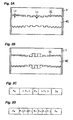
Figs. 2A to 2J are plan views showing modifications of the first embodiment; -
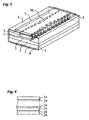
Fig. 3 is a perspective view of a high mesa type semiconductor laser according to a second embodiment of the present invention; and -
Fig. 4 is a cross sectional view showing a modification of an active layer. -
Fig. 1A shows a ridge type laser according to the first embodiment of the present invention. Formed on an n-type (001) GaAs substrate 1 by molecular beam epitaxy (MBE) are: an n-type Al0.4Ga0.6As clad layer 2 having a thickness of 1.4 µm; anactive layer 3 including multiple quantum dot layers; a p-type Al0.4Ga0.6As clad layer 4 having a thickness of 1.4 µm; and a p-typeGaAs contact layer 5 having a thickness of 0.4 µm. - As shown in
Fig. 1B , theactive layer 3 having ten quantum dot layers is formed by the following processes. After aGaAs barrier layer 3b having a thickness of, e.g., 36 nm is grown, InAs having a large lattice mismatch is grown in molecular layer order to form an InAs quantum dot layer 3qd by a self formation method in Stranski-Krastanov growth mode (S-K mode) which forms quantum dots at a thickness larger than a critical thickness. This InAs quantum dot layer is covered with aGaAs barrier layer 3b having a thickness of 36 nm. Further, pairs of similar InAs quantum dot layer 3qd andGaAs barrier layer 3b having the thickness of 36 nm are grown nine times. For formation of a quantum dot layer, for example, refer to paragraphs [0013] to [0070] of publishedJapanese Patent No. 3672678 US Patent No. 3,672,527 ). An InGaAs cap layer 3c may be formed on theGaAs barrier layer 3b to adjust an oscillation wavelength. - Reverting to
Fig. 1A , a silicon oxide layer having a thickness of, e.g., 300 nm is formed on the semiconductor layer structure by chemical vapor deposition (CVD) or the like, and an electron beam resist film is coated on the silicon oxide layer. A pattern of a ridge waveguide and a diffraction grating is exposed in the electron beam resist film, and is developed to form the electron beam resist pattern. The resist pattern is transferred to the silicon oxide layer to form a hard mask. A propagation direction of the waveguide is referred to below as the length direction, and the transverse direction as the width direction. - As shown in
Fig. 1C , a mask pattern MP has a diffraction grating portion DG on both sides of a ridge waveguide portion WG, and has, for example, a total width of 6 µm and a total effective length of 500 µm. The waveguide portion WG has: wide portions (wide width portions) WGw at opposite ends having a width of 4 µm and a length of 125 µm; a narrow portion (narrow width portion) WGn in a central area having a width of 1.5 µm and a length of 50 µm; and tapered intermediate portions WGi between the wide portions and the narrow portion having a length of 100 µm and gradually changing the waveguide width in a range from that of the narrow portion to that of the wide portions. The waveguide width of the intermediate portion WGi changes gradually and linearly from the waveguide width of WGn to WGw. The diffraction grating DG is constituted of end portions DGw, a central portion DGn and intermediate portions DGi along the length direction (propagation direction) in correspondence with the structure of the waveguide portions, the widths of these portions being the total width of 6 µm subtracted by the corresponding waveguide widths. In other words, the end portions DGw are relatively narrow and central portion DGn is relatively wide when considered in the transverse direction. -
Fig. 1D shows a schematic structure of the diffraction grating portion DG. When the waveguide width changes, an effective refractive index changes also. A change occurs, therefore, in a period of the diffraction grating for selectively reflecting light of a target wavelength. A pitch of the diffraction grating DGw is set to 192.6 nm, and a pitch of the diffraction grating DGn is set to 193.1 nm. In the intermediate portion DGi where the waveguide width changes gradually, the diffraction grating pitch is changed between 192.6 nm and 193.1 nm, for example, linearly. Although the pitch of the diffraction grating changes, a selected wavelength is the same at about 1.28 µm when the effective refractive index is taken into consideration. - A length of a tooth portion of the diffraction grating (a length of the diffraction grating) along the waveguide width direction (transverse direction) is equal to the width of the diffraction grating portion DG. The tooth portion length is 1 µm in the portion DGw, and 2.25 µm in the portion DGn. As the diffraction grating length of the portion DGn is elongated, it becomes possible to enhance selectivity of the fundamental transverse mode in this portion.
- Reverting to
Fig. 1A , by using a hard mask MP as an etching mask, the semiconductor layers layer is anisotropically etched from the surface thereof by mixture gas of (Br2 + N2) or the like, to a depth partially leaving a thickness of the p-type clad layer 4 or to a depth exposing theuppermost barrier layer 3b. In this manner, a ridge type waveguide structure is formed having vertical (i.e. perpendicular to the propagation direction and transverse direction) groove diffraction gratings on the sidewalls. The ridge type waveguide is buried in an insulator 6 such as ultraviolet ray curing resin, the insulator being transparent to a target wavelength. - Current injection electrodes 7 and 8 are formed on the top and bottom surfaces of the waveguide structure. Opposite ends of the waveguide structure are cleaved to form a cavity. If necessary, a reflection film or
films 9 made of dielectric multilayer and having a desired reflectivity is/are formed on an end surface or end surfaces. -
Fig. 1E shows an example of thereflection film 9. A silicon oxide film as a low refractive index film nL and a silicon film as a high refractive index film nH are alternately stacked to realize a desired reflectivity. For example, one pair of a stacked low refractive index film and high refractive index film realizes a reflectivity of 80 %, and two pairs of a stacked low refractive index film and high refractive index film realize a reflectivity of 93 to 95 %. An antireflection film may be formed by a single low refractive index film or multilayer of low refractive index film and high refractive index film. In the structure shown inFig. 1A , an antireflection film is formed. For a semiconductor laser manufacture method, a well-known method may be used, as disclosed, for example, in Oku et al. : IEEE Journal of Selected Topics in Quantum Electronics, Vol. 5, No. 3, p. 682, 1999. - It has been found from calculations that in the embodiment structure, a loss is not generated in the fundamental transverse mode, although a loss of about 50 % is generated in the higher first order transverse mode. It can be understood that the higher order transverse mode is suppressed. As compared to a waveguide structure whose waveguide width is set to 1.5 µm over the whole device length, an ohmic contact area on the top surface of the device is increased about twice, so an increase in a device resistance can be suppressed.
- The size of each portion of the device described above is only illustrative, and can have various different sizes. For example, if the narrow portion WGn is 0.8 µm wide, although a loss is generated in the fundamental transverse mode, a loss of about 93 % is generated in the higher first order transverse mode. The higher first order transverse mode is thus suppressed considerably. In this case, as compared to a waveguide structure whose waveguide width is set to 0.8 µm over the whole device length, an ohmic contact area on the top surface of the device is increased about 3.8 times, and an increase in a device resistance can be suppressed.
- If the length of the wide portion WGw is changed to 50 µm and the length of the narrow portion WGn is changed to 200 µm, a loss is not generated in the fundamental transverse mode and a loss of about 70 % is generated in the higher first order transverse mode. The higher order transverse mode can be suppressed effectively. As compared to a waveguide structure of 1.5 µm width over the whole device length, an ohmic contact area on the top surface of the device is increased about 1.6 times, and an increase in a device resistance can be suppressed. In this manner, by generating a loss of 50 % or more in the higher order transverse mode, it becomes possible to suppress the higher order transverse mode and efficiently extract the fundamental transverse mode. In the following, modifications of the first embodiment will be described.
-
Fig. 2A shows a structure in which a tooth length of the diffraction grating along the waveguide width direction (transverse direction) is made constant over the whole device length. The tooth length of diffraction grating from the wide width portion DGw toward the narrow width portion DGn has a constant value Lc. Although the suppression effect of the higher order transverse mode is reduced and a threshold gain in the fundamental transverse mode rises slightly, there is still a considerable higher order transverse mode suppression effect whilst limiting the increase in resistance. -
Fig. 2B shows a structure wherein the width of the whole ridge structure including the waveguide structure and diffraction grating structure is changed along the device length direction. It is not necessary to set the whole ridge structure width constant. In this structure, although the whole ridge structure is made wider in the narrow width portion, the whole structure may alternatively be made narrower in the narrow portion of the waveguide. -
Fig. 2C is a schematic diagram showing a structure in which the diffraction grating pitch in the intermediate portion DGi is set to a constant pitch Pi which takes an intermediate value between a pitch Pn of the diffraction grating in the narrow waveguide portion and a pitch Pw of the diffraction grating in the wide waveguide portion. In this case, the mask forming process can be simplified. -
Fig. 2D is a schematic diagram showing a structure in which the diffraction grating pitch in the intermediate portion DGi is set stepwise to values Pi1, Pi2 and Pi3 between the pitch Pn and the pitch Pw. -
Fig. 2E shows the structure where a pitch of the diffraction grating is set to a constant value Pc in the narrow portion DGn, intermediate portions DGn and wide portions DGw. Although the wavelength selectivity is lowered slightly, there still exist the higher order transverse mode suppression effect and the device resistance increase suppression effect. -
Fig. 2F shows a structure wherein the waveguide width of the intermediate portion WGi is not changed continuously but set to an intermediate width between that of WGw and WGn. The waveguide width of the intermediate portion may be changed stepwise. Although the wavelength selectivity is lowered slightly, and loss is increased at connection portions, there exist the higher order transverse mode suppression effect and the device resistance increase suppression effect. -
Fig. 2G shows a structure in which no diffraction grating is formed in the intermediate portion WGi. This reduces wavelength selectivity, but the higher order transverse mode suppression effect and the device resistance increase suppression effect are still obtained. -
Fig. 2H shows a structure in which a wide waveguide portion WGw is formed at one end of the waveguide, a narrow portion WGn is formed at the other end, and an intermediate portion WGi connects these two portions. Although at least one narrow portion and at least one wide portion of the waveguide are necessary, the layout of these portions may be changed in various ways. -
Fig. 2I shows a structure in which no diffraction grating is present at the waveguide portions WGw and WGi, but is present at the portion WGn. Alternatively, instead of forming the diffraction grating only in the narrow waveguide portion WGn, the diffraction grating may be formed only in the wide portion WGw. An antireflection film is not formed at the end where the diffraction grating is not formed. A high reflection film may be used. If a DFB laser is to be formed, it is necessary to form the diffraction grating on the end surface side where theantireflection film 9 is formed. -
Fig. 2J shows a structure wherein a plurality of narrow width portions WGn are formed so as to be distributed over the total device length. The number of narrow width portions can be varied depending upon a resonator length. It is, however, preferable to set the waveguide width of the narrow portion to 75 % or less of the waveguide width of the wide portion. - The modifications described above may be combined in various ways as appropriate.
-
Fig. 3 shows a structure of a DFB semiconductor laser of a high mesa structure according to the second embodiment of the present invention. Similar to the first embodiment, formed on an n-type (001) GaAs substrate 1 by molecular beam epitaxy (MBE) are: an n-type Al0.4Ga0.6As clad layer 2 having a thickness of 1.4 µm; anactive layer 3 including multiple quantum dot layers; a p-type Al0.4Ga0.6As clad layer 4 having a thickness of 1.4 µm; and a p-typeGaAs contact layer 5 having a thickness of 0.4 µm. - A silicon oxide layer having a thickness of, e.g., 300 nm is formed on the above semiconductor layer structure by chemical vapor deposition (CVD) or the like, and an electron beam resist film is coated on the silicon oxide layer. A pattern of a ridge waveguide and a diffraction grating is exposed in the electron beam resist film, and is developed to form the electron beam resist pattern. The resist pattern is transferred to the silicon oxide layer to form a hard mask.
- By using the hard mask as an etching mask, the semiconductor layers are etched from the surface thereof through the p-
type contact layer 5, p-type clad layer 4 andactive layer 3, to an intermediate depth of the n-type clad layer 2. In this manner, a high mesa type waveguide structure is formed having vertical groove diffraction gratings on the sidewalls. The high mesa type waveguide is buried in an insulator 6 such as ultraviolet ray curing resin, the insulator being transparent to a target wavelength. Current injection electrodes 7 and 8 are formed on the top and bottom surfaces of the waveguide structure. Opposite ends of the waveguide structure are cleaved to form a cavity. If necessary, a reflection film orfilms 9 having desired reflectivity is/are formed on an end surface or end surfaces. A semiconductor laser of the high mesa structure can be formed in the manner described above. Also in this embodiment, modifications such as those shown inFigs. 2A to 2J are possible. -
Fig. 4 shows a modification of theactive layer 3. Abarrier layer 3b and a well layer 3w are alternately stacked, both end layers being thebarrier layer 3b. An active layer of multilayer quantum well structure is therefore formed. - The present invention has been described in connection with the preferred embodiments. The invention is not limited only to the above embodiments. For example, although in the above description GaAs/AlGaAs/InAs based materials are stacked on the GaAs substrate, InP/GaInAsP based materials or AlGaInAs based materials may be stacked on an InP substrate. Quantum dots may be made of InAsSb or the like. Instead of a quantum dot active layer, a quantum well active layer, a quantum wire active layer, or a bulk active layer may also be used. The active layer may be doped. All conductivity types may be reversed. A high resistance substrate may also be used. Instead of an active DFB laser or DRB laser having the totally active layer over the whole device length, a DBR laser including a passive waveguide may be formed. It will be apparent to those skilled in the art that other various modifications, improvements, combinations, and the like can be made.
Claims (18)
- An optical semiconductor device comprising:a waveguide structure defining a propagation direction and having a width defined by sidewalls of the waveguide structure, and including a wide portion WGw, a narrow portion WGn, and an intermediate portion WGi connecting said wide portion WGw and said narrow portion WGn, formed along the propagation direction; anda diffraction grating DG formed on the sidewalls of at least one of said wide portion WGw and said narrow portion WGn of said waveguide structure, said diffraction grating DG having grooves perpendicular to the sidewalls and periodically disposed along the propagation direction and defining a wavelength of propagation light, and characterized in thatthe wide portion WGw has a constant first width and a first length, the narrow portion WGn has a constant second width and a second length and is narrower than said wide portion WGw, and the intermediate portion WGi has a width that changes gradually and linearly from the first width to the second width,wherein said narrow portion WGn has a second width and a length such that a loss of 50 % or more is imparted to a higher order transverse mode of the device.
- The optical semiconductor device according to claim 1, wherein the width of said narrow portion WGn of the waveguide structure is 75 % or less of the width of said wide portion.
- The optical semiconductor device according to claim 1, wherein both ends of said waveguide structure are cleaved to form a cavity.
- The optical semiconductor device according to claim 3, further comprising a reflection film (9) formed on at least one of end surfaces of said cavity.
- The optical semiconductor device according to any preceding claim, wherein said diffraction grating DG is formed on the sidewalls of both said wide portion WGw and said narrow portion WGn of said waveguide structure.
- The optical semiconductor device according to claim 5, wherein a pitch of said diffraction grating DG in said narrow portion WGn is longer than a pitch of said diffraction grating DG in said wide portion WGw.
- The optical semiconductor device according to claim 6, wherein each pitch of said diffraction grating DG in said narrow portion WG and said diffraction grating DG in said wide portion WGw is determined based on an equivalent refractive index of said waveguide structure so as to define the same propagation wavelength.
- The optical semiconductor device according to claim 5, wherein a lattice length of said diffraction grating DG in said narrow portion WGn along a waveguide width direction transverse to the propagation direction is longer than a lattice length of said diffraction grating DG in said wide portion WGw along the waveguide width direction.
- The optical semiconductor device according to claim 5, wherein said diffraction grating DG is formed also on the sidewalls of the intermediate portion WGi of said waveguide structure, and a pitch of said diffraction grating DG in said intermediate portion is set to a value in a range from a pitch of said diffraction grating DG in said wide portion WGw to a pitch of said diffraction grating DG in said narrow portion WGw.
- The optical semiconductor device according to claim 9, wherein a lattice length of said diffraction grating DG in said narrow portion WGn along a waveguide width direction is longer than a lattice length of said diffraction grating DG in said wide portion WGw along the waveguide width direction, and a lattice length of said diffraction grating DG in said intermediate portion along the waveguide width direction becomes gradually elongated from said wide portion WGw toward said narrow portion WGn.
- The optical semiconductor device according to any preceding claim, wherein said waveguide structure constitutes a ridge waveguide.
- The optical semiconductor device according to claim 11, wherein said layers include a lower clad layer (2), an active layer (3) and an upper clad layer (4) formed on a semiconductor substrate (1), and said waveguide structure is formed by etching said layers down to a surface of said upper clad layer (4).
- The optical semiconductor device according to any of claims 1 to 10, wherein said waveguide structure constitutes a high mesa waveguide.
- The optical semiconductor device according to claim 13, wherein said layers include a lower clad layer (2), an active layer (3) and an upper clad layer (4) formed on a semiconductor substrate (1), and said waveguide structure is formed by etching said layers through said upper clad layer (4) and said active layer (3).
- The optical semiconductor device according to claim 12, wherein said semiconductor substrate (1) is a GaAs substrate.
- The optical semiconductor device according to claim 15, wherein said active layer (3) contains InAs quantum dots.
- The optical semiconductor device according to claim 12, wherein said semiconductor substrate (1) is an InP substrate.
- The optical semiconductor device according to claim 17, wherein said active layer (3) contains InAsSb quantum dots.
Applications Claiming Priority (1)
| Application Number | Priority Date | Filing Date | Title |
|---|---|---|---|
| JP2006065791A JP2007243019A (en) | 2006-03-10 | 2006-03-10 | Optical semiconductor device |
Publications (2)
| Publication Number | Publication Date |
|---|---|
| EP1833128A1 EP1833128A1 (en) | 2007-09-12 |
| EP1833128B1 true EP1833128B1 (en) | 2009-10-14 |
Family
ID=38024354
Family Applications (1)
| Application Number | Title | Priority Date | Filing Date |
|---|---|---|---|
| EP07103717A Not-in-force EP1833128B1 (en) | 2006-03-10 | 2007-03-07 | Optical semiconductor device with diffraction grating |
Country Status (4)
| Country | Link |
|---|---|
| US (1) | US7738523B2 (en) |
| EP (1) | EP1833128B1 (en) |
| JP (1) | JP2007243019A (en) |
| DE (1) | DE602007002731D1 (en) |
Families Citing this family (28)
| Publication number | Priority date | Publication date | Assignee | Title |
|---|---|---|---|---|
| US8227178B2 (en) * | 2009-08-25 | 2012-07-24 | Fujikura Ltd. | Manufacturing method of planar optical waveguide device with grating structure |
| JP5625387B2 (en) * | 2010-02-26 | 2014-11-19 | 日亜化学工業株式会社 | Semiconductor laser device and manufacturing method thereof |
| US8649639B2 (en) * | 2010-03-04 | 2014-02-11 | Luxtera, Inc. | Method and system for waveguide mode filters |
| US8396091B2 (en) * | 2011-01-31 | 2013-03-12 | Technische Universitat Berlin | Device comprising a laser |
| WO2015099764A1 (en) | 2013-12-27 | 2015-07-02 | Intel Corporation | Asymmetric optical waveguide grating resonators & dbr lasers |
| JP6274224B2 (en) | 2014-01-10 | 2018-02-07 | 富士通株式会社 | Optical semiconductor device and manufacturing method thereof |
| US9991677B2 (en) * | 2014-05-13 | 2018-06-05 | California Institute Of Technology | Index-coupled distributed-feedback semiconductor quantum cascade lasers fabricated without epitaxial regrowth |
| US20170317471A1 (en) * | 2014-11-10 | 2017-11-02 | Agency For Science, Technology And Research | An optical device and a method for fabricating thereof |
| US9316787B1 (en) * | 2015-05-08 | 2016-04-19 | International Business Machines Corporation | Continuous evanescent perturbation gratings in a silicon photonic device |
| JP6998774B2 (en) * | 2016-01-13 | 2022-02-10 | 古河電気工業株式会社 | Semiconductor laser devices, chip-on-submounts, and semiconductor laser modules |
| JP6581024B2 (en) * | 2016-03-15 | 2019-09-25 | 株式会社東芝 | Distributed feedback laser diode |
| EP3635827B1 (en) * | 2017-05-08 | 2024-01-17 | Thorlabs Quantum Electronics, Inc. | Distributed feedback interband cascade lasers with corrugated sidewall |
| CN107482477B (en) * | 2017-07-28 | 2019-09-10 | 长春理工大学 | High-power distributed feedback semiconductor laser modulated by surface and side medium grating |
| US11061186B2 (en) * | 2018-11-26 | 2021-07-13 | Globalfoundries U.S. Inc. | Waveguide structures |
| CN109830891B (en) * | 2019-03-12 | 2020-10-09 | 南京大学 | Narrow linewidth semiconductor laser |
| CN110112650B (en) * | 2019-05-13 | 2020-06-02 | 苏州长光华芯半导体激光创新研究院有限公司 | High-power semiconductor chip and preparation method thereof |
| JP7340974B2 (en) * | 2019-07-18 | 2023-09-08 | パナソニックホールディングス株式会社 | Nitride semiconductor laser device |
| US11456573B2 (en) | 2019-10-02 | 2022-09-27 | California Institute Of Technology | Tapered-grating single mode lasers and method of manufacturing |
| CN111262130B (en) * | 2020-03-10 | 2022-04-19 | 常州纵慧芯光半导体科技有限公司 | Laser structure and preparation method and application thereof |
| JP7384734B2 (en) * | 2020-04-07 | 2023-11-21 | パナソニックホールディングス株式会社 | semiconductor laser device |
| CN111769436B (en) * | 2020-07-07 | 2021-09-28 | 因林光电科技(苏州)有限公司 | Distributed feedback laser chip and preparation method thereof |
| FR3118333B1 (en) | 2020-12-18 | 2023-07-14 | Commissariat Energie Atomique | Laser comprising a distributed Bragg mirror and method of production |
| FR3118332B1 (en) * | 2020-12-18 | 2023-07-14 | Commissariat Energie Atomique | Laser comprising a distributed Bragg mirror and production method |
| JP7662035B2 (en) * | 2021-06-24 | 2025-04-15 | 日本電信電話株式会社 | Semiconductor laser |
| JP7639631B2 (en) * | 2021-09-21 | 2025-03-05 | ウシオ電機株式会社 | Semiconductor light emitting device and method for manufacturing the same |
| US12620773B2 (en) * | 2022-04-28 | 2026-05-05 | Nexus Photonics, Inc. | Performance heterogeneous lasers and active components |
| US12492992B2 (en) | 2022-06-21 | 2025-12-09 | California Institute Of Technology | Spectroscopy device incorporating a mid-infrared laser |
| CN115224586B (en) * | 2022-06-22 | 2025-12-19 | 潍坊先进光电芯片研究院 | Surface random slot semiconductor laser applied to refractive index sensing |
Family Cites Families (13)
| Publication number | Priority date | Publication date | Assignee | Title |
|---|---|---|---|---|
| US4783788A (en) * | 1985-12-16 | 1988-11-08 | Lytel Incorporated | High power semiconductor lasers |
| JPS63260185A (en) * | 1987-04-17 | 1988-10-27 | Sony Corp | Distributed feedback type semiconductor laser |
| JPH01206681A (en) * | 1988-02-15 | 1989-08-18 | Canon Inc | Semiconductor laser and its manufacturing method |
| DE4322164A1 (en) * | 1993-07-03 | 1995-01-12 | Ant Nachrichtentech | Optoelectronic component with feedback grating, with axially quasi-continuous and almost arbitrarily variable grating coupling coefficients, with quasi-continuously axially distributable refractive index variation, and with axially almost arbitrarily distributable and variable phase shift |
| JP2950302B2 (en) * | 1997-11-25 | 1999-09-20 | 日本電気株式会社 | Semiconductor laser |
| JP2001133647A (en) * | 1999-08-20 | 2001-05-18 | Nippon Telegr & Teleph Corp <Ntt> | Waveguide type higher mode filter and semiconductor laser |
| JP2002299759A (en) * | 2001-04-02 | 2002-10-11 | Furukawa Electric Co Ltd:The | Semiconductor laser device |
| WO2003023817A2 (en) * | 2001-07-20 | 2003-03-20 | The Board Of Trustees Of The University Of Illinois | Process for forming semiconductor quantum dots with superior structural and morphological stability |
| EP1283571B1 (en) * | 2001-08-06 | 2015-01-14 | nanoplus GmbH Nanosystems and Technologies | Laser with weakly coupled grating |
| JP2003152273A (en) * | 2001-11-08 | 2003-05-23 | Furukawa Electric Co Ltd:The | Semiconductor laser device |
| US20050259699A1 (en) * | 2002-05-15 | 2005-11-24 | Bookham Technology, Ptc | Tuneable laser |
| WO2005060058A1 (en) * | 2003-12-18 | 2005-06-30 | Nec Corporation | Semiconductor laser and its manufacturing method |
| GB2416427A (en) * | 2004-06-18 | 2006-01-25 | Univ Sheffield | DFB laser |
-
2006
- 2006-03-10 JP JP2006065791A patent/JP2007243019A/en active Pending
-
2007
- 2007-03-07 DE DE602007002731T patent/DE602007002731D1/en not_active Expired - Fee Related
- 2007-03-07 EP EP07103717A patent/EP1833128B1/en not_active Not-in-force
- 2007-03-09 US US11/716,017 patent/US7738523B2/en not_active Expired - Fee Related
Also Published As
| Publication number | Publication date |
|---|---|
| US7738523B2 (en) | 2010-06-15 |
| DE602007002731D1 (en) | 2009-11-26 |
| EP1833128A1 (en) | 2007-09-12 |
| US20070248134A1 (en) | 2007-10-25 |
| JP2007243019A (en) | 2007-09-20 |
Similar Documents
| Publication | Publication Date | Title |
|---|---|---|
| US7738523B2 (en) | Optical semiconductor device having diffraction grating | |
| US10811842B2 (en) | Distributed feedback laser based on surface grating | |
| US7496127B2 (en) | Optical device coupling light propagating in optical waveguide with diffraction grating | |
| US9431793B2 (en) | Semiconductor laser device | |
| US8705583B2 (en) | Semiconductor laser | |
| US8319229B2 (en) | Optical semiconductor device and method for manufacturing the same | |
| US7835418B2 (en) | Optical semiconductor device having diffraction grating disposed on both sides of waveguide and its manufacture method | |
| US8716044B2 (en) | Optical semiconductor device having ridge structure formed on active layer containing P-type region and its manufacture method | |
| EP2686921B1 (en) | P-type isolation regions adjacent to facets of semiconductor quantum cascade laser | |
| JP4909159B2 (en) | Semiconductor waveguide device, manufacturing method thereof, and semiconductor laser | |
| EP0614254B1 (en) | Gain-coupling distributed feedback semiconductor laser and method of producing the same | |
| US6396863B1 (en) | High-power semiconductor laser device having index-guided structure with InAlGaP current confinement layer | |
| JP5287886B2 (en) | Optical device in which light propagating in optical waveguide and diffraction grating are coupled | |
| JP2009054721A (en) | Semiconductor device and method for manufacturing semiconductor device | |
| JP5057477B2 (en) | Semiconductor laser element | |
| US6600770B2 (en) | High-power semiconductor laser device having current confinement structure and index-guided structure and stably oscillating in single mode | |
| Okumura et al. | Lateral current injection type GaInAsP/InP DFB lasers on SI-InP substrate | |
| JP5702262B2 (en) | Tunable semiconductor laser | |
| JP2012033975A (en) | Method of manufacturing semiconductor laser | |
| JP2002532907A (en) | Gain-coupled distributed feedback semiconductor laser | |
| US20040151224A1 (en) | Distributed feedback semiconductor laser oscillating at longer wavelength mode and its manufacture method | |
| JP2009238796A (en) | Semiconductor laser, and method of manufacturing semiconductor laser | |
| JP2009194290A (en) | Semiconductor laser manufacturing method and semiconductor laser | |
| JP2009206126A (en) | Method for manufacturing semiconductor laser, and semiconductor laser | |
| JPH0927653A (en) | Semiconductor laser device |
Legal Events
| Date | Code | Title | Description |
|---|---|---|---|
| PUAI | Public reference made under article 153(3) epc to a published international application that has entered the european phase |
Free format text: ORIGINAL CODE: 0009012 |
|
| AK | Designated contracting states |
Kind code of ref document: A1 Designated state(s): AT BE BG CH CY CZ DE DK EE ES FI FR GB GR HU IE IS IT LI LT LU LV MC MT NL PL PT RO SE SI SK TR |
|
| AX | Request for extension of the european patent |
Extension state: AL BA HR MK YU |
|
| 17P | Request for examination filed |
Effective date: 20071001 |
|
| AKX | Designation fees paid |
Designated state(s): DE FR GB |
|
| GRAP | Despatch of communication of intention to grant a patent |
Free format text: ORIGINAL CODE: EPIDOSNIGR1 |
|
| GRAS | Grant fee paid |
Free format text: ORIGINAL CODE: EPIDOSNIGR3 |
|
| GRAA | (expected) grant |
Free format text: ORIGINAL CODE: 0009210 |
|
| AK | Designated contracting states |
Kind code of ref document: B1 Designated state(s): DE FR GB |
|
| REG | Reference to a national code |
Ref country code: GB Ref legal event code: FG4D |
|
| REF | Corresponds to: |
Ref document number: 602007002731 Country of ref document: DE Date of ref document: 20091126 Kind code of ref document: P |
|
| PLBE | No opposition filed within time limit |
Free format text: ORIGINAL CODE: 0009261 |
|
| STAA | Information on the status of an ep patent application or granted ep patent |
Free format text: STATUS: NO OPPOSITION FILED WITHIN TIME LIMIT |
|
| 26N | No opposition filed |
Effective date: 20100715 |
|
| REG | Reference to a national code |
Ref country code: FR Ref legal event code: ST Effective date: 20101130 |
|
| PG25 | Lapsed in a contracting state [announced via postgrant information from national office to epo] |
Ref country code: FR Free format text: LAPSE BECAUSE OF NON-PAYMENT OF DUE FEES Effective date: 20100331 |
|
| PG25 | Lapsed in a contracting state [announced via postgrant information from national office to epo] |
Ref country code: DE Free format text: LAPSE BECAUSE OF NON-PAYMENT OF DUE FEES Effective date: 20101001 |
|
| PGFP | Annual fee paid to national office [announced via postgrant information from national office to epo] |
Ref country code: GB Payment date: 20110328 Year of fee payment: 5 |
|
| GBPC | Gb: european patent ceased through non-payment of renewal fee |
Effective date: 20120307 |
|
| PG25 | Lapsed in a contracting state [announced via postgrant information from national office to epo] |
Ref country code: GB Free format text: LAPSE BECAUSE OF NON-PAYMENT OF DUE FEES Effective date: 20120307 |