EP1832673A1 - Method for producing substrate for single crystal diamond growth - Google Patents
Method for producing substrate for single crystal diamond growth Download PDFInfo
- Publication number
- EP1832673A1 EP1832673A1 EP07004683A EP07004683A EP1832673A1 EP 1832673 A1 EP1832673 A1 EP 1832673A1 EP 07004683 A EP07004683 A EP 07004683A EP 07004683 A EP07004683 A EP 07004683A EP 1832673 A1 EP1832673 A1 EP 1832673A1
- Authority
- EP
- European Patent Office
- Prior art keywords
- substrate
- single crystal
- crystal diamond
- producing
- bias treatment
- Prior art date
- Legal status (The legal status is an assumption and is not a legal conclusion. Google has not performed a legal analysis and makes no representation as to the accuracy of the status listed.)
- Granted
Links
Images
Classifications
-
- C—CHEMISTRY; METALLURGY
- C30—CRYSTAL GROWTH
- C30B—SINGLE-CRYSTAL GROWTH; UNIDIRECTIONAL SOLIDIFICATION OF EUTECTIC MATERIAL OR UNIDIRECTIONAL DEMIXING OF EUTECTOID MATERIAL; REFINING BY ZONE-MELTING OF MATERIAL; PRODUCTION OF A HOMOGENEOUS POLYCRYSTALLINE MATERIAL WITH DEFINED STRUCTURE; SINGLE CRYSTALS OR HOMOGENEOUS POLYCRYSTALLINE MATERIAL WITH DEFINED STRUCTURE; AFTER-TREATMENT OF SINGLE CRYSTALS OR A HOMOGENEOUS POLYCRYSTALLINE MATERIAL WITH DEFINED STRUCTURE; APPARATUS THEREFOR
- C30B25/00—Single-crystal growth by chemical reaction of reactive gases, e.g. chemical vapour-deposition growth
- C30B25/02—Epitaxial-layer growth
- C30B25/18—Epitaxial-layer growth characterised by the substrate
-
- C—CHEMISTRY; METALLURGY
- C30—CRYSTAL GROWTH
- C30B—SINGLE-CRYSTAL GROWTH; UNIDIRECTIONAL SOLIDIFICATION OF EUTECTIC MATERIAL OR UNIDIRECTIONAL DEMIXING OF EUTECTOID MATERIAL; REFINING BY ZONE-MELTING OF MATERIAL; PRODUCTION OF A HOMOGENEOUS POLYCRYSTALLINE MATERIAL WITH DEFINED STRUCTURE; SINGLE CRYSTALS OR HOMOGENEOUS POLYCRYSTALLINE MATERIAL WITH DEFINED STRUCTURE; AFTER-TREATMENT OF SINGLE CRYSTALS OR A HOMOGENEOUS POLYCRYSTALLINE MATERIAL WITH DEFINED STRUCTURE; APPARATUS THEREFOR
- C30B29/00—Single crystals or homogeneous polycrystalline material with defined structure characterised by the material or by their shape
- C30B29/02—Elements
- C30B29/04—Diamond
-
- H—ELECTRICITY
- H10—SEMICONDUCTOR DEVICES; ELECTRIC SOLID-STATE DEVICES NOT OTHERWISE PROVIDED FOR
- H10P—GENERIC PROCESSES OR APPARATUS FOR THE MANUFACTURE OR TREATMENT OF DEVICES COVERED BY CLASS H10
- H10P14/00—Formation of materials, e.g. in the shape of layers or pillars
- H10P14/20—Formation of materials, e.g. in the shape of layers or pillars of semiconductor materials
- H10P14/24—Formation of materials, e.g. in the shape of layers or pillars of semiconductor materials using chemical vapour deposition [CVD]
-
- H—ELECTRICITY
- H10—SEMICONDUCTOR DEVICES; ELECTRIC SOLID-STATE DEVICES NOT OTHERWISE PROVIDED FOR
- H10P—GENERIC PROCESSES OR APPARATUS FOR THE MANUFACTURE OR TREATMENT OF DEVICES COVERED BY CLASS H10
- H10P14/00—Formation of materials, e.g. in the shape of layers or pillars
- H10P14/20—Formation of materials, e.g. in the shape of layers or pillars of semiconductor materials
- H10P14/29—Formation of materials, e.g. in the shape of layers or pillars of semiconductor materials characterised by the substrates
- H10P14/2901—Materials
- H10P14/2921—Materials being crystalline insulating materials
-
- H—ELECTRICITY
- H10—SEMICONDUCTOR DEVICES; ELECTRIC SOLID-STATE DEVICES NOT OTHERWISE PROVIDED FOR
- H10P—GENERIC PROCESSES OR APPARATUS FOR THE MANUFACTURE OR TREATMENT OF DEVICES COVERED BY CLASS H10
- H10P14/00—Formation of materials, e.g. in the shape of layers or pillars
- H10P14/20—Formation of materials, e.g. in the shape of layers or pillars of semiconductor materials
- H10P14/29—Formation of materials, e.g. in the shape of layers or pillars of semiconductor materials characterised by the substrates
- H10P14/2926—Crystal orientations
-
- H—ELECTRICITY
- H10—SEMICONDUCTOR DEVICES; ELECTRIC SOLID-STATE DEVICES NOT OTHERWISE PROVIDED FOR
- H10P—GENERIC PROCESSES OR APPARATUS FOR THE MANUFACTURE OR TREATMENT OF DEVICES COVERED BY CLASS H10
- H10P14/00—Formation of materials, e.g. in the shape of layers or pillars
- H10P14/20—Formation of materials, e.g. in the shape of layers or pillars of semiconductor materials
- H10P14/32—Formation of materials, e.g. in the shape of layers or pillars of semiconductor materials characterised by intermediate layers between substrates and deposited layers
- H10P14/3202—Materials thereof
- H10P14/3204—Materials thereof being Group IVA semiconducting materials
- H10P14/3206—Carbon, e.g. diamond-like carbon
-
- H—ELECTRICITY
- H10—SEMICONDUCTOR DEVICES; ELECTRIC SOLID-STATE DEVICES NOT OTHERWISE PROVIDED FOR
- H10P—GENERIC PROCESSES OR APPARATUS FOR THE MANUFACTURE OR TREATMENT OF DEVICES COVERED BY CLASS H10
- H10P14/00—Formation of materials, e.g. in the shape of layers or pillars
- H10P14/20—Formation of materials, e.g. in the shape of layers or pillars of semiconductor materials
- H10P14/32—Formation of materials, e.g. in the shape of layers or pillars of semiconductor materials characterised by intermediate layers between substrates and deposited layers
- H10P14/3202—Materials thereof
- H10P14/3241—Materials thereof being conductive materials
-
- H—ELECTRICITY
- H10—SEMICONDUCTOR DEVICES; ELECTRIC SOLID-STATE DEVICES NOT OTHERWISE PROVIDED FOR
- H10P—GENERIC PROCESSES OR APPARATUS FOR THE MANUFACTURE OR TREATMENT OF DEVICES COVERED BY CLASS H10
- H10P14/00—Formation of materials, e.g. in the shape of layers or pillars
- H10P14/20—Formation of materials, e.g. in the shape of layers or pillars of semiconductor materials
- H10P14/34—Deposited materials, e.g. layers
- H10P14/3402—Deposited materials, e.g. layers characterised by the chemical composition
- H10P14/3404—Deposited materials, e.g. layers characterised by the chemical composition being Group IVA materials
- H10P14/3406—Carbon, e.g. diamond-like carbon
-
- H—ELECTRICITY
- H10—SEMICONDUCTOR DEVICES; ELECTRIC SOLID-STATE DEVICES NOT OTHERWISE PROVIDED FOR
- H10P—GENERIC PROCESSES OR APPARATUS FOR THE MANUFACTURE OR TREATMENT OF DEVICES COVERED BY CLASS H10
- H10P14/00—Formation of materials, e.g. in the shape of layers or pillars
- H10P14/20—Formation of materials, e.g. in the shape of layers or pillars of semiconductor materials
- H10P14/36—Formation of materials, e.g. in the shape of layers or pillars of semiconductor materials characterised by treatments done before the formation of the materials
-
- H—ELECTRICITY
- H10—SEMICONDUCTOR DEVICES; ELECTRIC SOLID-STATE DEVICES NOT OTHERWISE PROVIDED FOR
- H10P—GENERIC PROCESSES OR APPARATUS FOR THE MANUFACTURE OR TREATMENT OF DEVICES COVERED BY CLASS H10
- H10P14/00—Formation of materials, e.g. in the shape of layers or pillars
- H10P14/20—Formation of materials, e.g. in the shape of layers or pillars of semiconductor materials
- H10P14/29—Formation of materials, e.g. in the shape of layers or pillars of semiconductor materials characterised by the substrates
- H10P14/2901—Materials
- H10P14/2923—Materials being conductive materials, e.g. metallic silicides
Definitions
- the present invention relates to a method for producing a substrate for single crystal diamond growth.
- Diamond has a wide band gap of 5.47 eV and a very high dielectric breakdown electric field intensity of 10 MV/cm. Furthermore, it has the highest thermal conductivity in materials. Therefore, if this is used for an electronic device, the device is advantageous as a high output power device.
- diamond has high drift mobility and is the most advantageous as a highspeed power device in semiconductors in comparison of Johnson performance index.
- diamond is said to be the ultimate semiconductor suitable for high frequency / high power electronic devices.
- the Ib-type diamonds contain a large amount of nitrogen impurities and can only be obtained at a size of no more than about a 5-mm squar. Therefore, their utility is low.
- a so-called bias treatment for forming a nucleus of diamond on a substrate before single crystal diamond growth by a direct-current discharge in which an electrode in a substrate side is a cathode has been performed.
- a substrate for single crystal diamond growth has been produced by performing such a bias treatment at an Ir substrate temperature of 900°C before the diamond growth. And, it has been reported that on the substrate, the diamond growth is performed by a DC plasma CVD method, and thereby a diamond grain having a uniform orientation can be grown.
- the present invention has been made to solve the above-mentioned problems, and a main object of the present invention is to provide a method for producing a substrate for single crystal diamond growth, by which a single crystal diamond can be grown more certainly.
- the present invention is made in order to solve the above problems, the present invention provides a method for producing a substrate for single crystal diamond growth, comprising at least a step of preliminarily subjecting a substrate before single crystal diamond growth to a bias treatment for forming a diamond nucleus thereon by a direct-current discharge in which an electrode in a substrate side is a cathode, and wherein in the treatment, at least, a temperature of the substrate from 40 sec after an initiation of the bias treatment to an end of the bias treatment is held in a range of 800°C ⁇ 60°C.
- a single crystal diamond can be grown more certainly.
- a current density in the bias treatment is set in a range of 120 to 230 mA/cm 2 .
- a treatment time of the bias treatment is set in a range of 45 sec to 180 sec.
- an atmosphere in the bias treatment is a mixed gas containing carbon and hydrogen atoms, a pressure of the atmosphere is in a range of 105 to 150 Torr.
- a substrate for single crystal diamond growth of the present invention it is possible that as the substrate for single crystal diamond growth before the bias treatment, a single crystal iridium (Ir) is used.
- the substrate for single crystal diamond growth before the bias treatment an Ir film grown heteroepitaxially on a single crystal MgO substrate is used.
- the present invention provides a method for producing a multilayer substrate, comprising a step of, performing growth on the above-described bias-treated substrate by a microwave CVD method or a direct-current plasma CVD method under a condition of a substrate temperature of 700°C to 1400°C, and thereby producing a multilayer substrate including a single crystal diamond.
- the present invention provides a multilayer substrate including a single crystal diamond produced by the above-described method.
- the present invention provides an independent single crystal diamond substrate that is only a diamond taken out of the multilayer substrate produced by the method.
- the present invention provides a device fabricated by using the above-described multilayer substrate including a single crystal diamond or the above-described independent single crystal diamond substrate.
- the present inventor has found that when the bias treatment is performed with setting a temperature of the substrate to be in a predetermined range, a single crystal diamond can be more certainly grown on the treated substrate, and thereby has accomplished the present invention.
- the method for producing a substrate for single crystal diamond growth of the present invention comprises at least a step of preliminarily subjecting a substrate before single crystal diamond growth to a bias treatment for forming a diamond nucleus thereon by a direct-current discharge in which an electrode in a substrate side is a cathode, and wherein in the treatment, at least, a temperature of the substrate from 40 sec after an initiation of the bias treatment to an end of the bias treatment is held in a range of 800°C ⁇ 60°C.
- a temperature of the substrate from 40 sec after an initiation of the bias treatment to an end of the bias treatment is held in a range of 800°C ⁇ 60°C as described above.
- amorphous carbon is formed on the substrate and on the other hand, a diamond nucleus is not formed. Also, in a subsequent diamond growth process, a single crystal diamond is not grown. Reversely, at a higher temperature (higher than 860°C) than this most appropriate temperature range, etching of the surface progresses and the diamond nucleus is not formed, and also in a subsequent diamond growth process, diamond is not grown.
- the measurement of the substrate temperature can be performed, for example, as follows.
- the temperature of the substrate surface can be measured by the radiation thermometer IR-CAI2CS manufactured by CHINO CORPORATION.
- the detection device is InGaAs, the measurement wavelength is 1.55 ⁇ m, and the temperature in the range of 300°C to 1600°C can be measured.
- the surface of the substrate which is an object to be measured is Ir, and that a radiation rate determined by crystallinity, surface shape, measurement temperature, measurement wavelength, and so forth, is set.
- the radiation rate may be set to 0.3, which is a generally known radiation rate of a solid Ir in a wavelength of 0.65 ⁇ m (See, page 15 of instruction book: CHINO INST No. Ir-274-P5CE).
- the actual measurement can be performed by, for example, setting a radiation thermometer outside a chamber using a tripod, and aligning the sight on a surface of the substrate in the chamber through a quartz window provided in the chamber.
- a current density in the bias treatment is set in a range of 120 to 230 mA/cm 2 .
- a treatment time of the bias treatment is set in a range of 45 sec to 180 sec.
- an atmosphere in the bias treatment is a mixed gas containing carbon and hydrogen atoms, a pressure of the atmosphere is in a range of 105 to 150 Torr.
- the substrate for diamond growth to be used in the bias treatment the following substrate can be used.
- a single crystal iridium (Ir) can be used as the substrate for diamond growth before the bias treatment.
- an Ir film grown heteroepitaxially on a single crystal MgO substrate can be used as the substrate for diamond growth before the bias treatment.
- the present invention provides a method for producing a multilayer substrate, comprising a step of, performing growth on the above-described bias-treated substrate by a microwave CVD method or a direct-current plasma CVD method under a condition of a substrate temperature of 700°C to 1400°C, and thereby producing a multilayer substrate including a single crystal diamond.
- the present invention provides a multilayer substrate including a single crystal diamond produced by the above-described method.
- the present invention provides an independent single crystal diamond substrate that is only a diamond taken out of the multilayer substrate produced by the above-described method.
- the present invention provides a device fabricated by using the above-described multilayer substrate including a single crystal diamond or the above-described independent single crystal diamond substrate.
- an Ir film was heteroepitaxially grown on the side of this MgO substrate on which a diamond film would be formed.
- an Ir film was further grown on the back surface thereof.
- the substrate was set on an electrode for applying a negative voltage (cathode), and vacuum evacuation was performed.
- the substrate was heated (the first heating), and the temperature of the substrate was raised to 648°C for 5 min (Fig. 1 (a)).
- a CH 4 /H 2 gas was introduced, and the base pressure was set to 115 Torr.
- the substrate was heated again (the second heating), and the temperature of the substrate was raised to 461°C for 5 min (Fig. 1 (b)) .
- the bias treatment was performed. That is, a DC voltage (345 mA) was applied. At this time, the temperature of the substrate was raised to 800°C for 40 sec, and further to 810°C for 90 sec (Fig. 1 (c)).
- the obtained multilayer substrate was confirmed, and therefore, it was possible to confirm that a single crystal diamond could be grown.
- Example 2 In the same manner as Example 1, an Ir film was heteroepitaxially grown on the side of the MgO substrate on which a diamond film would be formed. For electric connection, an Ir film was further grown on the back surface thereof.
- the substrate was set on an electrode for applying a negative voltage (cathode), and vacuum evacuation was performed.
- the substrate was heated (the first heating), and the temperature of the substrate was raised to 538°C for 5 min (Fig. 2 (a)) .
- a CH 4 /H 2 gas was introduced, and the base pressure was set to 115 Torr.
- the substrate was heated again (the second heating), and the temperature of the substrate was raised to 423°C for 5 min (Fig. 2 (b)).
- the bias treatment was performed. That is, a DC voltage (280 mA) was applied. At this time, the temperature of the substrate was raised to 720°C for 40 sec, and further to 799°C for 90 sec (Fig. 2 (c)).
- the obtained multilayer substrate was confirmed, and therefore, it was confirmed that a single crystal diamond could not be grown.
- Example 2 In the same manner as Example 1, an Ir film was heteroepitaxially grown on the side of the MgO substrate on which a diamond film would be formed. For electric connection, an Ir film was further grown on the back surface thereof.
- the obtained multilayer substrate was confirmed, and therefore, it was confirmed that a single crystal diamond could not be grown.
Landscapes
- Chemical & Material Sciences (AREA)
- Engineering & Computer Science (AREA)
- Crystallography & Structural Chemistry (AREA)
- Materials Engineering (AREA)
- Metallurgy (AREA)
- Organic Chemistry (AREA)
- Chemical Kinetics & Catalysis (AREA)
- General Chemical & Material Sciences (AREA)
- Crystals, And After-Treatments Of Crystals (AREA)
- Chemical Vapour Deposition (AREA)
Abstract
Description
- The present invention relates to a method for producing a substrate for single crystal diamond growth.
- Diamond has a wide band gap of 5.47 eV and a very high dielectric breakdown electric field intensity of 10 MV/cm. Furthermore, it has the highest thermal conductivity in materials. Therefore, if this is used for an electronic device, the device is advantageous as a high output power device.
- On the other hand, diamond has high drift mobility and is the most advantageous as a highspeed power device in semiconductors in comparison of Johnson performance index.
- Accordingly, diamond is said to be the ultimate semiconductor suitable for high frequency / high power electronic devices.
- Therefore, a multilayer substrate in which a diamond film and the like is laminated on a substrate has attracted attention.
- Now, most of the single crystal diamonds for fabrication of a diamond semiconductor are diamonds referred to as Ib type formed by a highpressure method. The Ib-type diamonds contain a large amount of nitrogen impurities and can only be obtained at a size of no more than about a 5-mm squar. Therefore, their utility is low.
- By contrast, there is an advantage that by Chemical Vapor Deposition (CVD) method, a diamond of a relatively large area can be obtained with high purity.
- Before growing a diamond film by this CVD method, a so-called bias treatment for forming a nucleus of diamond on a substrate before single crystal diamond growth by a direct-current discharge in which an electrode in a substrate side is a cathode has been performed.
- For example, in Jpn. J. Appl. Phys. Vol. 35(1996) pp. L1072-L1074 and NEW DIAMOND, Vol. 18 No. 4, (2002), pp. 6-12, a substrate for single crystal diamond growth has been produced by performing such a bias treatment at an Ir substrate temperature of 900°C before the diamond growth. And, it has been reported that on the substrate, the diamond growth is performed by a DC plasma CVD method, and thereby a diamond grain having a uniform orientation can be grown.
- Moreover, in 65th Japan Society of Applied Physics Academic Lecture Preliminary Report No. 2 (2004), pp. 508, it has been described that the bias treatment is performed at an Ir substrate temperature of 920°C before the diamond growth, and it has been reported that the same result as the above-described Jpn. J. Appl. Phys. Vol. 35(1996) pp. L1072-L1074 and NEW DIAMOND, Vol. 18 No. 4, (2002), pp. 6-12 can be obtained.
- However, the above-described Jpn. J. Appl. Phys. Vol. 35(1996) pp. L1072-L1074, NEW DIAMOND, Vol. 18 No. 4, (2002), pp. 6-12, and 65th Japan Society of Applied Physics Academic Lecture Preliminary Report No. 2 (2004), pp. 508 do not quite describe details about a method for measuring the temperature of the substrate, a condition thereof, a place for the measurement, and so forth. Furthermore, in experiments by the present inventor, even when any one of the other conditions complies with a condition described in the above-described Jpn. J. Appl. Phys. Vol. 35(1996) pp. L1072-L1074 NEW DIAMOND, Vol. 18 No. 4, (2002), pp. 6-12, or 65th Japan Society of Applied Physics Academic Lecture Preliminary Report No. 2 (2004), pp. 508, it has been impossible to grow a single crystal diamond, on the substrate subjected to the bias treatment at approximately 900°C.
- The present invention has been made to solve the above-mentioned problems, and a main object of the present invention is to provide a method for producing a substrate for single crystal diamond growth, by which a single crystal diamond can be grown more certainly.
- The present invention is made in order to solve the above problems, the present invention provides a method for producing a substrate for single crystal diamond growth, comprising at least a step of preliminarily subjecting a substrate before single crystal diamond growth to a bias treatment for forming a diamond nucleus thereon by a direct-current discharge in which an electrode in a substrate side is a cathode, and wherein in the treatment, at least, a temperature of the substrate from 40 sec after an initiation of the bias treatment to an end of the bias treatment is held in a range of 800°C ± 60°C.
- By, at least, holding a temperature of the substrate from 40 sec after an initiation of the bias treatment to an end of the bias treatment to be in a range of 800°C ± 60°C in the bias treatment as described above, a single crystal diamond can be grown more certainly.
- Moreover, in the method for producing a substrate for single crystal diamond growth of the present invention, it is preferable that a current density in the bias treatment is set in a range of 120 to 230 mA/cm2.
- Moreover, in the method for producing a substrate for single crystal diamond growth of the present invention, it is preferable that a treatment time of the bias treatment is set in a range of 45 sec to 180 sec.
- Moreover, in the method for producing a substrate for single crystal diamond growth of the present invention, it is preferable that an atmosphere in the bias treatment is methane diluted with hydrogen, and a concentration of the hydrogen-diluted methane is set in a range of CH4/(CH4+H2) = 0.5 to 5.0 vol.%.
- Moreover, in the method for producing a substrate for single crystal diamond growth of the present invention, it is preferable that an atmosphere in the bias treatment is a mixed gas containing carbon and hydrogen atoms, a pressure of the atmosphere is in a range of 105 to 150 Torr.
- Moreover, in the method for producing a substrate for single crystal diamond growth of the present invention, it is possible that as the substrate for single crystal diamond growth before the bias treatment, a single crystal iridium (Ir) is used.
- Alternatively, it is possible that as the substrate for single crystal diamond growth before the bias treatment, an Ir film grown heteroepitaxially on a single crystal MgO substrate is used.
- Furthermore, the present invention provides a method for producing a multilayer substrate, comprising a step of, performing growth on the above-described bias-treated substrate by a microwave CVD method or a direct-current plasma CVD method under a condition of a substrate temperature of 700°C to 1400°C, and thereby producing a multilayer substrate including a single crystal diamond.
- Moreover, the present invention provides a multilayer substrate including a single crystal diamond produced by the above-described method.
- Moreover, the present invention provides an independent single crystal diamond substrate that is only a diamond taken out of the multilayer substrate produced by the method.
- Furthermore, the present invention provides a device fabricated by using the above-described multilayer substrate including a single crystal diamond or the above-described independent single crystal diamond substrate.
- As described above, by using the method for producing a substrate for single crystal diamond growth of the present invention, a single crystal diamond can be grown more certainly.
-
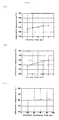
- Fig. 1 is a graph showing the change of the substrate temperature before the bias treatment and in the bias treatment (Example 1).
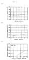
- Fig. 2 is a graph showing the change of the substrate temperature before the bias treatment and in the bias treatment (Comparative example 1).
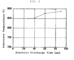
- Fig. 3 is a graph showing the change of the substrate temperature in the bias treatment (Comparative example 2).
- Hereinafter, embodiments of the present invention will be explained. However, the present invention is not limited thereto.
- As described above, conventionally, even if a bias treatment is performed in order to preliminarily form a nucleus of diamond, there is a problem that a single crystal diamond cannot certainly grown on a substrate subjected to the bias treatment. Therefore, the present inventor has thoroughly investigated the condition of the bias treatment.
- As a result, the present inventor has found that when the bias treatment is performed with setting a temperature of the substrate to be in a predetermined range, a single crystal diamond can be more certainly grown on the treated substrate, and thereby has accomplished the present invention.
- That is, the method for producing a substrate for single crystal diamond growth of the present invention comprises at least a step of preliminarily subjecting a substrate before single crystal diamond growth to a bias treatment for forming a diamond nucleus thereon by a direct-current discharge in which an electrode in a substrate side is a cathode, and wherein in the treatment, at least, a temperature of the substrate from 40 sec after an initiation of the bias treatment to an end of the bias treatment is held in a range of 800°C ± 60°C.
- In order to grow a single crystal diamond more certainly, it is necessary that in the bias treatment, a temperature of the substrate from 40 sec after an initiation of the bias treatment to an end of the bias treatment is held in a range of 800°C ± 60°C as described above.
- At a lower temperature (less than 740°C) than this most appropriate temperature range, amorphous carbon is formed on the substrate and on the other hand, a diamond nucleus is not formed. Also, in a subsequent diamond growth process, a single crystal diamond is not grown. Reversely, at a higher temperature (higher than 860°C) than this most appropriate temperature range, etching of the surface progresses and the diamond nucleus is not formed, and also in a subsequent diamond growth process, diamond is not grown.
- Here, the measurement of the substrate temperature can be performed, for example, as follows.
- The temperature of the substrate surface can be measured by the radiation thermometer IR-CAI2CS manufactured by CHINO CORPORATION.
- In the radiation thermometer, the detection device is InGaAs, the measurement wavelength is 1.55 µm, and the temperature in the range of 300°C to 1600°C can be measured. In the measurement, it is necessary that the surface of the substrate which is an object to be measured is Ir, and that a radiation rate determined by crystallinity, surface shape, measurement temperature, measurement wavelength, and so forth, is set. However, because the strict setting is difficult, the radiation rate may be set to 0.3, which is a generally known radiation rate of a solid Ir in a wavelength of 0.65 µm (See, page 15 of instruction book: CHINO INST No. Ir-274-P5CE).
- The actual measurement can be performed by, for example, setting a radiation thermometer outside a chamber using a tripod, and aligning the sight on a surface of the substrate in the chamber through a quartz window provided in the chamber.
- Next, the other condition in the bias treatment will be described as follows.
- It is preferable that a current density in the bias treatment is set in a range of 120 to 230 mA/cm2.
- Moreover, it is preferable that a treatment time of the bias treatment is set in a range of 45 sec to 180 sec.
- Moreover, it is preferable that an atmosphere in the bias treatment is methane diluted with hydrogen, and a concentration of the hydrogen-diluted methane is set in a range of CH4/(CH4+H2) = 0.5 to 5.0 vol.%.
- Moreover, it is preferable that an atmosphere in the bias treatment is a mixed gas containing carbon and hydrogen atoms, a pressure of the atmosphere is in a range of 105 to 150 Torr.
- Next, as the substrate for diamond growth to be used in the bias treatment, the following substrate can be used.
- That is, as the substrate for diamond growth before the bias treatment, a single crystal iridium (Ir) can be used.
- Alternatively, as the substrate for diamond growth before the bias treatment, an Ir film grown heteroepitaxially on a single crystal MgO substrate can be used.
- Furthermore, the present invention provides a method for producing a multilayer substrate, comprising a step of, performing growth on the above-described bias-treated substrate by a microwave CVD method or a direct-current plasma CVD method under a condition of a substrate temperature of 700°C to 1400°C, and thereby producing a multilayer substrate including a single crystal diamond.
- Moreover, the present invention provides a multilayer substrate including a single crystal diamond produced by the above-described method.
- Moreover, the present invention provides an independent single crystal diamond substrate that is only a diamond taken out of the multilayer substrate produced by the above-described method.
- Furthermore, the present invention provides a device fabricated by using the above-described multilayer substrate including a single crystal diamond or the above-described independent single crystal diamond substrate.
- Hereinafter, the present invention will be explained more specifically with reference to Example and Comparative examples. However, the present invention is not limited thereto.
- A double-side polished single crystal MgO substrate having a 10.0-mm square, a 0.5-mm thickness, and an orientation (100), was prepared.
- And, an Ir film was heteroepitaxially grown on the side of this MgO substrate on which a diamond film would be formed. For electric connection, an Ir film was further grown on the back surface thereof.
- Next, the bias treatment for forming a nucleus of diamond on the surface of the Ir film of this substrate was performed.
- First, as the preparation before the bias treatment, the substrate was set on an electrode for applying a negative voltage (cathode), and vacuum evacuation was performed. Next, the substrate was heated (the first heating), and the temperature of the substrate was raised to 648°C for 5 min (Fig. 1 (a)). Next, a CH4/H2 gas was introduced, and the base pressure was set to 115 Torr. Next, the substrate was heated again (the second heating), and the temperature of the substrate was raised to 461°C for 5 min (Fig. 1 (b)) .
- Then, the bias treatment was performed. That is, a DC voltage (345 mA) was applied. At this time, the temperature of the substrate was raised to 800°C for 40 sec, and further to 810°C for 90 sec (Fig. 1 (c)).
- Last, on this substrate, a diamond was grown by a microwave (2.45 GHz) CVD method.
- The obtained multilayer substrate was confirmed, and therefore, it was possible to confirm that a single crystal diamond could be grown.
- In the same manner as Example 1, an Ir film was heteroepitaxially grown on the side of the MgO substrate on which a diamond film would be formed. For electric connection, an Ir film was further grown on the back surface thereof.
- Next, the bias treatment for forming a nucleus of diamond on the surface of the Ir film of this substrate was performed.
- First, as the preparation before the bias treatment, the substrate was set on an electrode for applying a negative voltage (cathode), and vacuum evacuation was performed. Next, the substrate was heated (the first heating), and the temperature of the substrate was raised to 538°C for 5 min (Fig. 2 (a)) . Next, a CH4/H2 gas was introduced, and the base pressure was set to 115 Torr. Next, the substrate was heated again (the second heating), and the temperature of the substrate was raised to 423°C for 5 min (Fig. 2 (b)).
- Then, the bias treatment was performed. That is, a DC voltage (280 mA) was applied. At this time, the temperature of the substrate was raised to 720°C for 40 sec, and further to 799°C for 90 sec (Fig. 2 (c)).
- Last, it was attempted to grow a diamond on this substrate by a microwave (2.45 GHz) CVD method.
- However, the obtained multilayer substrate was confirmed, and therefore, it was confirmed that a single crystal diamond could not be grown.
- In the same manner as Example 1, an Ir film was heteroepitaxially grown on the side of the MgO substrate on which a diamond film would be formed. For electric connection, an Ir film was further grown on the back surface thereof.
- Next, the bias treatment for forming a nucleus of diamond on the surface of the Ir film of this substrate was performed.
- That is, after the predetermined preparation before the treatment, a DC voltage (400 mA) was applied. At this time, the temperature of the substrate was raised to 852°C for 40 sec, and further to 887°C for 90 sec (Fig. 3).
- Last, it was attempted to grow a diamond on this substrate by a microwave (2.45 GHz) CVD method.
- However, the obtained multilayer substrate was confirmed, and therefore, it was confirmed that a single crystal diamond could not be grown.
- The present invention is not limited to the above-described embodiments. The above-described embodiments are mere examples and those having the substantially same constitution as that described in the appended claims and providing the similar functions and advantages are included in the scope of the present invention.
Claims (11)
- A method for producing a substrate for single crystal diamond growth, comprising at least a step of preliminarily subjecting a substrate before single crystal diamond growth to a bias treatment for forming a diamond nucleus thereon by a direct-current discharge in which an electrode in a substrate side is a cathode, and wherein in the treatment, at least, a temperature of the substrate from 40 sec after an initiation of the bias treatment to an end of the bias treatment is held in a range of 800°C ± 60°C.
- The method for producing a substrate for single crystal diamond growth according to Claim 1, wherein a current density in the bias treatment is set in a range of 120 to 230 mA/cm2.
- The method for producing a substrate for single crystal diamond growth according to Claim 1 or 2, wherein a treatment time of the bias treatment is set in a range of 45 sec to 180 sec.
- The method for producing a substrate for single crystal diamond growth according to any one of Claims 1 to 3, wherein an atmosphere in the bias treatment is methane diluted with hydrogen, and a concentration of the hydrogen-diluted methane is set in a range of CH4/(CH4+H2) = 0.5 to 5.0 vol.%.
- The method for producing a substrate for single crystal diamond growth according to any one of Claims 1 to 4, wherein an atmosphere in the bias treatment is a mixed gas containing carbon and hydrogen atoms, a pressure of the atmosphere is in a range of 105 to 150 Torr.
- The method for producing a substrate for single crystal diamond growth according to any one of Claims 1 to 5, wherein as the substrate for single crystal diamond growth before the bias treatment, a single crystal iridium (Ir) is used.
- The method for producing a substrate for single crystal diamond growth according to any one of Claims 1 to 5, wherein as the substrate for single crystal diamond growth before the bias treatment, an Ir film grown heteroepitaxially on a single crystal MgO substrate is used.
- A method for producing a multilayer substrate, comprising a step of, performing growth on the bias-treated substrate according to any one of Claims 1 to 7 by a microwave CVD method or a direct-current plasma CVD method under a condition of a substrate temperature of 700°C to 1400°C, and thereby producing a multilayer substrate including a single crystal diamond.
- A multilayer substrate including a single crystal diamond produced by the method according to Claim 8.
- An independent single crystal diamond substrate that is only a diamond taken out of the multilayer substrate produced by the method according to Claim 8.
- A device fabricated by using the multilayer substrate including the single crystal diamond according to Claim 9 or the independent single crystal diamond substrate according to Claim 10.
Applications Claiming Priority (1)
| Application Number | Priority Date | Filing Date | Title |
|---|---|---|---|
| JP2006063376A JP5053553B2 (en) | 2006-03-08 | 2006-03-08 | Method for producing substrate for single crystal diamond growth |
Publications (2)
| Publication Number | Publication Date |
|---|---|
| EP1832673A1 true EP1832673A1 (en) | 2007-09-12 |
| EP1832673B1 EP1832673B1 (en) | 2018-06-06 |
Family
ID=38068620
Family Applications (1)
| Application Number | Title | Priority Date | Filing Date |
|---|---|---|---|
| EP07004683.4A Active EP1832673B1 (en) | 2006-03-08 | 2007-03-07 | Method for producing substrate for single crystal diamond growth |
Country Status (6)
| Country | Link |
|---|---|
| US (1) | US7628856B2 (en) |
| EP (1) | EP1832673B1 (en) |
| JP (1) | JP5053553B2 (en) |
| KR (1) | KR101419741B1 (en) |
| CN (1) | CN101054720A (en) |
| TW (1) | TWI340183B (en) |
Cited By (1)
| Publication number | Priority date | Publication date | Assignee | Title |
|---|---|---|---|---|
| EP2009135A4 (en) * | 2006-03-31 | 2010-12-29 | Imai Yoshio | BASE SUBSTRATE FOR EPITAXIC DIAMOND FILM, METHOD FOR MANUFACTURING BASE SUBSTRATE FOR EPITAXIC DIAMOND FILM, EPITAXIC DIAMOND FILM MANUFACTURED BY THE BASE SUBSTRATE FOR EPITAXIC DIAMOND FILM, AND METHOD FOR FABRICATION |
Families Citing this family (11)
| Publication number | Priority date | Publication date | Assignee | Title |
|---|---|---|---|---|
| JP2010095408A (en) * | 2008-10-17 | 2010-04-30 | Agd Material Co Ltd | Method for manufacturing epitaxial diamond film and self-supporting epitaxial diamond substrate |
| JP2010159185A (en) * | 2009-01-09 | 2010-07-22 | Shin-Etsu Chemical Co Ltd | Multilayer substrate and method for manufacturing the same, and diamond film and method for manufacturing the same |
| JP4982506B2 (en) | 2009-01-09 | 2012-07-25 | 信越化学工業株式会社 | Method for producing single crystal diamond |
| JP5507888B2 (en) | 2009-05-20 | 2014-05-28 | 信越化学工業株式会社 | Single crystal diamond layer growth substrate and method for manufacturing single crystal diamond substrate |
| JP5377212B2 (en) | 2009-10-13 | 2013-12-25 | 信越化学工業株式会社 | Method for producing single crystal diamond substrate |
| JP5545567B2 (en) * | 2010-06-17 | 2014-07-09 | 国立大学法人金沢大学 | Base material for single crystal diamond growth and method for producing single crystal diamond |
| JP5468528B2 (en) * | 2010-06-28 | 2014-04-09 | 信越化学工業株式会社 | SUBSTRATE FOR GROWING SINGLE CRYSTAL DIAMOND, METHOD FOR PRODUCING THE SAME, AND METHOD FOR PRODUCING SINGLE CRYSTAL DIAMOND SUBSTRATE |
| JP5842761B2 (en) | 2012-08-07 | 2016-01-13 | 信越化学工業株式会社 | Diamond production method and DC plasma CVD apparatus |
| US10923859B2 (en) * | 2019-04-19 | 2021-02-16 | Intel Corporation | Crosstalk reducing connector pin geometry |
| FR3100924B1 (en) * | 2019-09-13 | 2022-02-04 | Commissariat Energie Atomique | Treatment of a thin film by hydrogen plasma and polarization to improve its crystalline quality |
| CN113430642B (en) * | 2021-06-29 | 2022-10-28 | 哈尔滨工业大学 | Method for reducing heteroepitaxial bias threshold |
Citations (5)
| Publication number | Priority date | Publication date | Assignee | Title |
|---|---|---|---|---|
| JPH0585892A (en) * | 1991-07-31 | 1993-04-06 | Nec Corp | Diamond thin film and its production |
| JPH08133892A (en) * | 1994-11-07 | 1996-05-28 | Sumitomo Electric Ind Ltd | Diamond synthesis |
| US5854495A (en) * | 1993-05-06 | 1998-12-29 | Kobe Steel Europe Limited | Preparation of nucleated silicon surfaces |
| US20040069209A1 (en) | 2002-08-27 | 2004-04-15 | Board Of Trustees Of Michigan State University | Heteroepitaxial diamond and diamond nuclei precursors |
| JP2005335988A (en) * | 2004-05-25 | 2005-12-08 | Tama Tlo Kk | Substrate with diamond film, diamond film, and method of their formation, semiconductor unit, optical device, microfilter, part for micromachine, decoration display substrate and grinding particle |
Family Cites Families (8)
| Publication number | Priority date | Publication date | Assignee | Title |
|---|---|---|---|---|
| JPH059735A (en) * | 1991-07-09 | 1993-01-19 | Kobe Steel Ltd | Vapor synthesis of diamond |
| US5397428A (en) * | 1991-12-20 | 1995-03-14 | The University Of North Carolina At Chapel Hill | Nucleation enhancement for chemical vapor deposition of diamond |
| JPH05194092A (en) * | 1992-01-24 | 1993-08-03 | Fuji Xerox Co Ltd | Thin diamond film, its preparation and thermal head provided with the same thin diamond film |
| JP3124422B2 (en) * | 1993-09-24 | 2001-01-15 | 株式会社神戸製鋼所 | Method of forming highly oriented diamond thin film |
| EP0689233B1 (en) * | 1994-06-24 | 2008-10-15 | Sumitomo Electric Industries, Limited | Wafer and method of producing same |
| JP3728467B2 (en) * | 1995-08-04 | 2005-12-21 | 株式会社神戸製鋼所 | Method for forming single crystal diamond film |
| JP2005219962A (en) * | 2004-02-05 | 2005-08-18 | Sumitomo Electric Ind Ltd | Diamond single crystal substrate and manufacturing method thereof |
| JP2006019649A (en) * | 2004-07-05 | 2006-01-19 | Kobe Steel Ltd | Diamond sensor and its manufacturing method |
-
2006
- 2006-03-08 JP JP2006063376A patent/JP5053553B2/en not_active Expired - Lifetime
-
2007
- 2007-01-12 KR KR1020070003837A patent/KR101419741B1/en active Active
- 2007-03-02 US US11/713,036 patent/US7628856B2/en active Active
- 2007-03-07 EP EP07004683.4A patent/EP1832673B1/en active Active
- 2007-03-08 CN CNA2007100858830A patent/CN101054720A/en active Pending
- 2007-03-08 TW TW096107993A patent/TWI340183B/en active
Patent Citations (5)
| Publication number | Priority date | Publication date | Assignee | Title |
|---|---|---|---|---|
| JPH0585892A (en) * | 1991-07-31 | 1993-04-06 | Nec Corp | Diamond thin film and its production |
| US5854495A (en) * | 1993-05-06 | 1998-12-29 | Kobe Steel Europe Limited | Preparation of nucleated silicon surfaces |
| JPH08133892A (en) * | 1994-11-07 | 1996-05-28 | Sumitomo Electric Ind Ltd | Diamond synthesis |
| US20040069209A1 (en) | 2002-08-27 | 2004-04-15 | Board Of Trustees Of Michigan State University | Heteroepitaxial diamond and diamond nuclei precursors |
| JP2005335988A (en) * | 2004-05-25 | 2005-12-08 | Tama Tlo Kk | Substrate with diamond film, diamond film, and method of their formation, semiconductor unit, optical device, microfilter, part for micromachine, decoration display substrate and grinding particle |
Non-Patent Citations (2)
| Title |
|---|
| ISHIGAKI NORITAKA ET AL: "OBSERVATION OF DIAMOND NUCLEATION DURING BIAS TREATMENT", NEW DIAMOND AND FRONTIER CARBON TECHNOLOGY, SCIENTIFIC PUBLISHING DIVISION OF MYU, TOKYO, JP, vol. 13, no. 6, 2003, pages 323 - 331, XP008079696, ISSN: 1344-9931 * |
| OHTSUKA K ET AL: "EPITAXIAL GROWTH OF DIAMOND ON IRIDIUM", JAPANESE JOURNAL OF APPLIED PHYSICS, JAPAN SOCIETY OF APPLIED PHYSICS, TOKYO, JP, vol. 35, no. 8B, 15 August 1996 (1996-08-15), pages L1072 - L1074, XP000733045, ISSN: 0021-4922 * |
Cited By (1)
| Publication number | Priority date | Publication date | Assignee | Title |
|---|---|---|---|---|
| EP2009135A4 (en) * | 2006-03-31 | 2010-12-29 | Imai Yoshio | BASE SUBSTRATE FOR EPITAXIC DIAMOND FILM, METHOD FOR MANUFACTURING BASE SUBSTRATE FOR EPITAXIC DIAMOND FILM, EPITAXIC DIAMOND FILM MANUFACTURED BY THE BASE SUBSTRATE FOR EPITAXIC DIAMOND FILM, AND METHOD FOR FABRICATION |
Also Published As
| Publication number | Publication date |
|---|---|
| US20070209578A1 (en) | 2007-09-13 |
| TW200801260A (en) | 2008-01-01 |
| CN101054720A (en) | 2007-10-17 |
| KR101419741B1 (en) | 2014-07-15 |
| US7628856B2 (en) | 2009-12-08 |
| JP5053553B2 (en) | 2012-10-17 |
| TWI340183B (en) | 2011-04-11 |
| JP2007238377A (en) | 2007-09-20 |
| KR20070092098A (en) | 2007-09-12 |
| EP1832673B1 (en) | 2018-06-06 |
Similar Documents
| Publication | Publication Date | Title |
|---|---|---|
| EP1832673B1 (en) | Method for producing substrate for single crystal diamond growth | |
| CN102041551B (en) | Base material for growing single crystal diamond and method for producing single crystal diamond substrate | |
| Stoner et al. | Highly oriented, textured diamond films on silicon via bias-enhanced nucleation and textured growth | |
| US20120225308A1 (en) | Multilayer substrate and method for producing the same, diamond film and method for producing the same | |
| EP2048267B1 (en) | Process for producing single-crystal substrate with off angle | |
| US10066317B2 (en) | Method for manufacturing a single crystal diamond | |
| US20110081531A1 (en) | Base material for growing single crystal diamond and method for producing single crystal diamond substrate | |
| US9752255B2 (en) | Base material on which single-crystal diamond is grown comprised of a base substrate, bonded single-crystal MgO layer, and heteroepitaxial film, and method for manufacturing a single-crystal diamond substrate on the base material | |
| TWI787234B (en) | Base substrate for diamond film formation, and method for manufacturing diamond substrate using same | |
| EP0617147A2 (en) | Diamond crystal forming method | |
| US9410241B2 (en) | Method for separating surface layer or growth layer of diamond | |
| US7514146B2 (en) | Multilayer substrate, method for producing a multilayer substrate, and device | |
| JP2016204748A (en) | Gallium nitride-based film and production method thereof | |
| EP2226413B1 (en) | Method for manufacturing diamond monocrystal having a thin film, and diamond monocrystal having a thin film. | |
| EP2276060A1 (en) | PROCESS FOR PRODUCING SI(1-V-W-X)CWALXNV BASE MATERIAL, PROCESS FOR PRODUCING EPITAXIAL WAFER, SI(1-V-W-X)CWALXNVBASE MATERIAL, AND EPITAXIAL WAFER & xA; | |
| EP4357492A1 (en) | Diamond substrate and manufacturing method for same | |
| TW202403082A (en) | Base substrate and single crystal diamond laminated substrate and methods of manufacturing the same | |
| Altukhov et al. | Characterization of single-crystal diamond grown from the vapor phase on substrates of natural diamond | |
| Reshi et al. | Fabrication and characterization of diamond as detector for future collider | |
| JPH0789794A (en) | Method for forming highly-oriented diamond thin film and device therefor | |
| Vodopyanov et al. | Monocrystalline InN films grown at high rate by organometallic vapor phase epitaxy with nitrogen plasma activation supported by gyrotron radiation | |
| CN119731377A (en) | Substrate, single crystal diamond laminate substrate, and method for producing same | |
| Zhao et al. | High-mobility, low-resistive boron-doped diamond material realized by oxygen assistance | |
| JP6944699B2 (en) | Method for manufacturing hexagonal boron nitride film | |
| TW202340507A (en) | Underlying substrate and single crystal diamond laminated substrate and their manufacturing method |
Legal Events
| Date | Code | Title | Description |
|---|---|---|---|
| PUAI | Public reference made under article 153(3) epc to a published international application that has entered the european phase |
Free format text: ORIGINAL CODE: 0009012 |
|
| AK | Designated contracting states |
Kind code of ref document: A1 Designated state(s): AT BE BG CH CY CZ DE DK EE ES FI FR GB GR HU IE IS IT LI LT LU LV MC MT NL PL PT RO SE SI SK TR |
|
| AX | Request for extension of the european patent |
Extension state: AL BA HR MK YU |
|
| 17P | Request for examination filed |
Effective date: 20080111 |
|
| AKX | Designation fees paid | ||
| RBV | Designated contracting states (corrected) |
Designated state(s): DE |
|
| RBV | Designated contracting states (corrected) |
Designated state(s): DE FR |
|
| RBV | Designated contracting states (corrected) |
Designated state(s): DE FR GB |
|
| RAP1 | Party data changed (applicant data changed or rights of an application transferred) |
Owner name: SHIN-ETSU CHEMICAL CO., LTD. |
|
| RAP1 | Party data changed (applicant data changed or rights of an application transferred) |
Owner name: SHIN-ETSU CHEMICAL CO., LTD. |
|
| RIN1 | Information on inventor provided before grant (corrected) |
Inventor name: SHINTARO MAEDA Inventor name: ATSUHITO SAWABE Inventor name: NOGUCHI, HITOSHI, C/O ADV. FUNCT. MAT. RES. CENTER |
|
| RAP1 | Party data changed (applicant data changed or rights of an application transferred) |
Owner name: SHIN-ETSU CHEMICAL CO., LTD. Owner name: AGD MATERIAL CO. |
|
| RIN1 | Information on inventor provided before grant (corrected) |
Inventor name: NOGUCHI, HITOSHIA Inventor name: SHINTARO MAEDA Inventor name: SAWABE, ATSUHITO |
|
| RIN1 | Information on inventor provided before grant (corrected) |
Inventor name: NOGUCHI, HITOSHIA Inventor name: SHINTARO MAEDA Inventor name: SAWABE, ATSUHITO |
|
| 17Q | First examination report despatched |
Effective date: 20110811 |
|
| RIC1 | Information provided on ipc code assigned before grant |
Ipc: C30B 25/18 20060101ALI20171213BHEP Ipc: C30B 29/04 20060101AFI20171213BHEP Ipc: H01L 21/02 20060101ALI20171213BHEP Ipc: H01L 29/00 20060101ALI20171213BHEP |
|
| GRAP | Despatch of communication of intention to grant a patent |
Free format text: ORIGINAL CODE: EPIDOSNIGR1 |
|
| STAA | Information on the status of an ep patent application or granted ep patent |
Free format text: STATUS: GRANT OF PATENT IS INTENDED |
|
| INTG | Intention to grant announced |
Effective date: 20180129 |
|
| GRAS | Grant fee paid |
Free format text: ORIGINAL CODE: EPIDOSNIGR3 |
|
| GRAA | (expected) grant |
Free format text: ORIGINAL CODE: 0009210 |
|
| STAA | Information on the status of an ep patent application or granted ep patent |
Free format text: STATUS: THE PATENT HAS BEEN GRANTED |
|
| AK | Designated contracting states |
Kind code of ref document: B1 Designated state(s): DE FR GB |
|
| REG | Reference to a national code |
Ref country code: GB Ref legal event code: FG4D |
|
| REG | Reference to a national code |
Ref country code: DE Ref legal event code: R096 Ref document number: 602007055028 Country of ref document: DE |
|
| REG | Reference to a national code |
Ref country code: DE Ref legal event code: R097 Ref document number: 602007055028 Country of ref document: DE |
|
| PLBE | No opposition filed within time limit |
Free format text: ORIGINAL CODE: 0009261 |
|
| STAA | Information on the status of an ep patent application or granted ep patent |
Free format text: STATUS: NO OPPOSITION FILED WITHIN TIME LIMIT |
|
| 26N | No opposition filed |
Effective date: 20190307 |
|
| PGFP | Annual fee paid to national office [announced via postgrant information from national office to epo] |
Ref country code: GB Payment date: 20260202 Year of fee payment: 20 |
|
| PGFP | Annual fee paid to national office [announced via postgrant information from national office to epo] |
Ref country code: DE Payment date: 20260128 Year of fee payment: 20 |
|
| PGFP | Annual fee paid to national office [announced via postgrant information from national office to epo] |
Ref country code: FR Payment date: 20260209 Year of fee payment: 20 |