EP1831966B1 - Cap for an electrical connector - Google Patents
Cap for an electrical connector Download PDFInfo
- Publication number
- EP1831966B1 EP1831966B1 EP05815228A EP05815228A EP1831966B1 EP 1831966 B1 EP1831966 B1 EP 1831966B1 EP 05815228 A EP05815228 A EP 05815228A EP 05815228 A EP05815228 A EP 05815228A EP 1831966 B1 EP1831966 B1 EP 1831966B1
- Authority
- EP
- European Patent Office
- Prior art keywords
- cap
- electrical connector
- center
- connector
- substrate
- Prior art date
- Legal status (The legal status is an assumption and is not a legal conclusion. Google has not performed a legal analysis and makes no representation as to the accuracy of the status listed.)
- Not-in-force
Links
Images


Classifications
-
- H—ELECTRICITY
- H05—ELECTRIC TECHNIQUES NOT OTHERWISE PROVIDED FOR
- H05K—PRINTED CIRCUITS; CASINGS OR CONSTRUCTIONAL DETAILS OF ELECTRIC APPARATUS; MANUFACTURE OF ASSEMBLAGES OF ELECTRICAL COMPONENTS
- H05K3/00—Apparatus or processes for manufacturing printed circuits
- H05K3/30—Assembling printed circuits with electric components, e.g. with resistor
- H05K3/32—Assembling printed circuits with electric components, e.g. with resistor electrically connecting electric components or wires to printed circuits
- H05K3/34—Assembling printed circuits with electric components, e.g. with resistor electrically connecting electric components or wires to printed circuits by soldering
- H05K3/3405—Edge mounted components, e.g. terminals
-
- H—ELECTRICITY
- H01—ELECTRIC ELEMENTS
- H01R—ELECTRICALLY-CONDUCTIVE CONNECTIONS; STRUCTURAL ASSOCIATIONS OF A PLURALITY OF MUTUALLY-INSULATED ELECTRICAL CONNECTING ELEMENTS; COUPLING DEVICES; CURRENT COLLECTORS
- H01R12/00—Structural associations of a plurality of mutually-insulated electrical connecting elements, specially adapted for printed circuits, e.g. printed circuit boards [PCB], flat or ribbon cables, or like generally planar structures, e.g. terminal strips, terminal blocks; Coupling devices specially adapted for printed circuits, flat or ribbon cables, or like generally planar structures; Terminals specially adapted for contact with, or insertion into, printed circuits, flat or ribbon cables, or like generally planar structures
- H01R12/70—Coupling devices
- H01R12/7005—Guiding, mounting, polarizing or locking means; Extractors
- H01R12/7011—Locking or fixing a connector to a PCB
- H01R12/707—Soldering or welding
-
- H—ELECTRICITY
- H01—ELECTRIC ELEMENTS
- H01R—ELECTRICALLY-CONDUCTIVE CONNECTIONS; STRUCTURAL ASSOCIATIONS OF A PLURALITY OF MUTUALLY-INSULATED ELECTRICAL CONNECTING ELEMENTS; COUPLING DEVICES; CURRENT COLLECTORS
- H01R12/00—Structural associations of a plurality of mutually-insulated electrical connecting elements, specially adapted for printed circuits, e.g. printed circuit boards [PCB], flat or ribbon cables, or like generally planar structures, e.g. terminal strips, terminal blocks; Coupling devices specially adapted for printed circuits, flat or ribbon cables, or like generally planar structures; Terminals specially adapted for contact with, or insertion into, printed circuits, flat or ribbon cables, or like generally planar structures
- H01R12/70—Coupling devices
- H01R12/71—Coupling devices for rigid printing circuits or like structures
- H01R12/72—Coupling devices for rigid printing circuits or like structures coupling with the edge of the rigid printed circuits or like structures
- H01R12/722—Coupling devices for rigid printing circuits or like structures coupling with the edge of the rigid printed circuits or like structures coupling devices mounted on the edge of the printed circuits
- H01R12/724—Coupling devices for rigid printing circuits or like structures coupling with the edge of the rigid printed circuits or like structures coupling devices mounted on the edge of the printed circuits containing contact members forming a right angle
-
- H—ELECTRICITY
- H01—ELECTRIC ELEMENTS
- H01R—ELECTRICALLY-CONDUCTIVE CONNECTIONS; STRUCTURAL ASSOCIATIONS OF A PLURALITY OF MUTUALLY-INSULATED ELECTRICAL CONNECTING ELEMENTS; COUPLING DEVICES; CURRENT COLLECTORS
- H01R13/00—Details of coupling devices of the kinds covered by groups H01R12/70 or H01R24/00 - H01R33/00
- H01R13/46—Bases; Cases
- H01R13/502—Bases; Cases composed of different pieces
-
- H—ELECTRICITY
- H01—ELECTRIC ELEMENTS
- H01R—ELECTRICALLY-CONDUCTIVE CONNECTIONS; STRUCTURAL ASSOCIATIONS OF A PLURALITY OF MUTUALLY-INSULATED ELECTRICAL CONNECTING ELEMENTS; COUPLING DEVICES; CURRENT COLLECTORS
- H01R13/00—Details of coupling devices of the kinds covered by groups H01R12/70 or H01R24/00 - H01R33/00
- H01R13/46—Bases; Cases
- H01R13/514—Bases; Cases composed as a modular blocks or assembly, i.e. composed of co-operating parts provided with contact members or holding contact members between them
-
- H—ELECTRICITY
- H01—ELECTRIC ELEMENTS
- H01R—ELECTRICALLY-CONDUCTIVE CONNECTIONS; STRUCTURAL ASSOCIATIONS OF A PLURALITY OF MUTUALLY-INSULATED ELECTRICAL CONNECTING ELEMENTS; COUPLING DEVICES; CURRENT COLLECTORS
- H01R43/00—Apparatus or processes specially adapted for manufacturing, assembling, maintaining, or repairing of line connectors or current collectors or for joining electric conductors
- H01R43/02—Apparatus or processes specially adapted for manufacturing, assembling, maintaining, or repairing of line connectors or current collectors or for joining electric conductors for soldered or welded connections
- H01R43/0263—Apparatus or processes specially adapted for manufacturing, assembling, maintaining, or repairing of line connectors or current collectors or for joining electric conductors for soldered or welded connections for positioning or holding parts during soldering or welding process
-
- H—ELECTRICITY
- H05—ELECTRIC TECHNIQUES NOT OTHERWISE PROVIDED FOR
- H05K—PRINTED CIRCUITS; CASINGS OR CONSTRUCTIONAL DETAILS OF ELECTRIC APPARATUS; MANUFACTURE OF ASSEMBLAGES OF ELECTRICAL COMPONENTS
- H05K2201/00—Indexing scheme relating to printed circuits covered by H05K1/00
- H05K2201/10—Details of components or other objects attached to or integrated in a printed circuit board
- H05K2201/10007—Types of components
- H05K2201/10189—Non-printed connector
-
- H—ELECTRICITY
- H05—ELECTRIC TECHNIQUES NOT OTHERWISE PROVIDED FOR
- H05K—PRINTED CIRCUITS; CASINGS OR CONSTRUCTIONAL DETAILS OF ELECTRIC APPARATUS; MANUFACTURE OF ASSEMBLAGES OF ELECTRICAL COMPONENTS
- H05K2201/00—Indexing scheme relating to printed circuits covered by H05K1/00
- H05K2201/10—Details of components or other objects attached to or integrated in a printed circuit board
- H05K2201/10431—Details of mounted components
- H05K2201/10439—Position of a single component
- H05K2201/10446—Mounted on an edge
-
- H—ELECTRICITY
- H05—ELECTRIC TECHNIQUES NOT OTHERWISE PROVIDED FOR
- H05K—PRINTED CIRCUITS; CASINGS OR CONSTRUCTIONAL DETAILS OF ELECTRIC APPARATUS; MANUFACTURE OF ASSEMBLAGES OF ELECTRICAL COMPONENTS
- H05K2203/00—Indexing scheme relating to apparatus or processes for manufacturing printed circuits covered by H05K3/00
- H05K2203/15—Position of the PCB during processing
- H05K2203/159—Using gravitational force; Processing against the gravity direction; Using centrifugal force
-
- H—ELECTRICITY
- H05—ELECTRIC TECHNIQUES NOT OTHERWISE PROVIDED FOR
- H05K—PRINTED CIRCUITS; CASINGS OR CONSTRUCTIONAL DETAILS OF ELECTRIC APPARATUS; MANUFACTURE OF ASSEMBLAGES OF ELECTRICAL COMPONENTS
- H05K3/00—Apparatus or processes for manufacturing printed circuits
- H05K3/30—Assembling printed circuits with electric components, e.g. with resistor
- H05K3/32—Assembling printed circuits with electric components, e.g. with resistor electrically connecting electric components or wires to printed circuits
- H05K3/34—Assembling printed circuits with electric components, e.g. with resistor electrically connecting electric components or wires to printed circuits by soldering
- H05K3/341—Surface mounted components
- H05K3/3431—Leadless components
- H05K3/3436—Leadless components having an array of bottom contacts, e.g. pad grid array or ball grid array components
Definitions
- the invention relates generally to electrical connectors. More specifically, the invention relates to a cap for an electrical connector that weights the connector to facilitate mounting of the connector on the surface of a substrate.
- solder connections act as electrical and mechanical connections between the substrate and contact pads on the connector.
- the weight of some BGA connectors is not distributed evenly across the solder balls (or other fusible elements).
- the center of gravity of some BGA connectors such as right angle BGA connectors, may be offset from the geometric center thereof to an extent that causes the connector to tilt (or tip) on the substrate.
- Such tilting can vary the pressures on the solders ball of the ball-grid array.
- the weight of the connector may be distributed unevenly among the solder balls.
- Such uneven distribution can result in differences in the collapsing properties and the height of the solder balls as the solder balls are melted to form electrical connections. These factors degrade the strength and integrity of the resulting solder connections.
- tilting can result in separation of the solder ball from the associated contact pad, thereby inhibiting the formation of an electrical connection.
- EP 1 146 596 and EP 1 376 763 disclose the removing or adding of material from/to the connector in order to balance the connector, and to suppress undesired skewing during the mounting process of the connector onto the substrate.
- a preferred embodiment for a method of mounting an electrical connector to a substrate includes placing an electrical connector onto a substrate so that a fusible element substantially aligns with the contact pad on the substrate, providing a cap for the electrical connector where the cap has a geometric center offset from its center of gravity, placing the cap onto the electrical connector to counterbalance and reposition the center of gravity of the electrical connector so that the weight of the combined assembly is centered over the fusible area, and heating the electrical connector and the substrate to create at least one electrical connection between the electrical connector and the substrate so that the fusible elements form into a common geometry.
- the cap itself is defined as below.
- a preferred embodiment of a cap for a electrical connector includes a body, where the body includes a substantially planar first surface suitable for vacuum pickup, a second surface formed to engage the electrical connector, and a center of gravity and a geometric center where the center of gravity is offset from the geometric center so that the cap balances the electrical connector on the substrate fusible area when the cap is placed on the electrical connector.
- a preferred embodiment of an assembly includes a substrate, where the substrate includes an upper side having at least one contact pad for connection, an electrical connector, where the electrical connector comprises a housing, an electrical conductor mounted within the housing, a fusible element attached to the electrical conductor for forming an electrical connection with the substrate, a center of gravity, and a geometric center, where the center of gravity of the electrical connector is offset from the geometric center of the electrical connector along at least one axis, and a cap for mating with the electrical connector, where the cap comprises a body with a center of gravity and a geometric center, where the center of gravity of the cap is offset from the geometric center of the cap so that the cap relocates the center of gravity of the combined assembly in alignment with the center of the fusible area when the cap is placed on the electrical connector.
- a preferred embodiment of a method for mounting a ball-grid array connector to a substrate includes placing the ball-grid array connector onto the substrate so that a fusible element array substantially aligns with an array of contact pads on the substrate, providing a cap for the ball-grid array connector, wherein the cap has a geometric center offset from its center of gravity, placing the cap onto the ball-grid array connector to counterbalance the ball-grid array connector, and heating the ball-grid array connector and the substrate to create at least one electrical connection between the ball-grid array connector and the substrate.
- Figure 1 is an exemplary view of a substrate and an electrical connector showing a fusible area
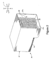
- Figure 2 is a perspective view of a right angle ball-grid array connector
- Figure 3 is an exemplary view of an insert molded leadframe assembly of the ball-grid array connector shown in Figure 2 ;
- Figure 4 is an exemplary view of the lower surface of a ball-grid array connector shown in Figure 2 ;
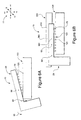
- Figure 5 is an exemplary exploded view of an electrical assembly including a substrate, an electrical connector, and a cap in a preferred embodiment of this invention
- Figure 6A is an exemplary view of a substrate and electrical connector
- Figure 6B is an exemplary view of a substrate, an electrical connector, and a cap.
- the cap 200 is described in conjunction with this particular type of connector for exemplary purposes only; alternative embodiments of the cap 200 can be configured for use with virtually any type of surface-mounted connector.
- the figures are each referenced to a common coordinate system 11 depicted therein.
- the connector 20 is shown as being mounted on a printed circuit board (PCB) 100.
- PCB printed circuit board
- the use of this particular type of substrate is depicted for exemplary purposes only.
- the connector 20 can be mounted on other types of substrates, such as printed wire boards, backplanes, etc.
- the connector 20 comprises an electrically-insulative housing 27, and a plurality of insert molded leadframe assemblies (IMLAs) 21 positioned within the housing 27 (see Figures 2 and 3 ).
- Each IMLA 21 includes a plurality of electrical conductors 22 that extend through an overmolded frame 24.
- the frame 24 is formed from a suitable electrically-insulative material such as plastic.
- Each electrical conductor 22 preferably includes a lead portion 26, a pin (not shown) adjoining a first end of the lead portion 26, and a blade contact 28 adjoining a second end of the lead portion 26.
- Each IMLA 21 can include fifteen of the electrical conductors 22.
- the electrical conductors 22 vary in length.
- the electrical conductors 22 are arranged side-by-side within the housing 27, so that the blade contacts 28 form a vertically-oriented column adjacent to the front edge of the frame 24, and the pins form a horizontally-oriented row along the bottom of the frame 24 (from the perspective of Figures 2 and 3 ).
- a fusible element is attached to each pin of the electrical conductors 22.
- the fusible element can be, for example, a solder ball 70.
- the solder balls 70 form a ball-grid array 71 on the bottom of the connector 20, as depicted in Figure 4 .
- the solder balls 70 each contact an associated contact pad 120 on the PCB 100 which defines the fusible area 122 when the connector 20 is mounted thereon, as discussed below.
- the electrical connector 20 has a mid-point (geometric center) 50, and a center of gravity 60.
- the electrical connector 20 is not symmetric about the geometric center 50, when viewed from the perspective of Figures 1 and 6A .
- the connector 20 is not symmetrically disposed about an axis extending in the "y" direction and passing through the geometric center 50.
- the center of gravity 60 therefore is offset from the geometric center 50 from the perspective of Figures 1 and 6A .
- the connector 20 is placed on the PCB 100 so that the solder balls 70 each substantially align with a corresponding contact pad 120 on the PCB 100, as noted above.
- the solder balls 70 are subsequently heated by a suitable process such as a reflow operation. The heating melts the solder balls 70.
- the solder upon cooling, forms electrical connections between the pins of the electrical conductors 22 and the associated contact pads 120.
- the above-noted offset in the center of gravity 60 of the connector 20 causes the center of gravity 60 to overhang the ball-grid array 71, as shown in Figures 1 , 5 and 6A .
- the weight of the connector 20 (acting through the center of gravity 60), in combination with the reactive force exerted by the PCB 100 on the connector 20 by way of the solder balls 70, generate a counterclockwise moment on the connector 20 (from the perspective of Figures 1 , 5 , and 6A ). This moment is denoted by the arrow 90 in Figures 1 , 5 , and 6A .
- the moment 90 if not counteracted, can cause the connector 20 to tilt, as shown in Figure 6A , thereby causing at least some of the solder balls 70 to lose contact with their corresponding contact pads 120 or to not have a common geometry.
- the cap 200 can act as a counterweight that counteracts the moment 90, thereby preventing the above-noted tilting of the connector 20.
- the cap 200 comprises a solid body 250 having a first surface 210 and a second surface 220.
- the first surface 210 preferably is planar, to facilitate pick-up of the cap 200 by a vacuum pickup.
- the second surface 220 is configured to engage the electrical connector 20.
- the second surface 220 defines a cavity 222.
- the shape of the cavity 222 is substantially similar to that of the uppermost portion of the connector 20, so that the cap 200 fits snugly over the connector 20, i.e., the cap 200 fits over the connector 20 with minimal clearance therebetween.
- the body 250 is configured so that the cap 200 acts as a counterweight to substantially balance the connector 20 when the connector 20 is placed on the PCB 100. This is achieved by configuring the body 250 to be non-symmetric about the mid-point (geometric center) thereof, from the perspective of Figure 5 .
- the geometric center of the body 250 is denoted in the figures by the reference numeral 260.
- the body 250 is non-symmetric about an axis extending the in "y" direction and passing through the geometric center 260.
- the body 250 is configured with a receiving portion 225, a first side portion 230 located to one side of the receiving portion 225 (from the perspective of Figure 5 ), and a second side portion 235 located to the other side of the receiving portion 225.
- the second side portion 235 is substantially larger than the first side portion 230, as shown in Figure 5 .
- the weight of the second side portion 235 therefore is substantially greater than that of the first side portion 230.
- This feature causes the weight of the body 250 to be distributed asymmetrically about the geometric center 260 (from the perspective of Figure 5 ).
- the center of gravity of the body 250 therefore is offset from the geometric center 260.
- the center of gravity of the body 250 is denoted in the figures by the reference numeral 270.
- the center of gravity 270 and the geometric center 260 are located at a different positions along the "x" axis denoted in the figures.
- Alternative embodiments of the cap 200 can comprise a body having two separate portions, a cap portion and a balancing portion, in contradistinction of the one-piece, homogenous cap 200.
- the balancing portion can be selectively positioned on the cap portion so that the combined cap portion and balancing portion perform the same balancing function as the cap 200.
- geometric center 260 and the center of gravity 270 are depicted diagrammatically; the geometric center 260 and the center of gravity 270 are not necessarily located at the positions depicted in the figures.
- the cap 200 preferably is constructed so that the cap 200 counterbalances the connector 20 when the connector 20 is placed on the PCB 100, as noted above. More specifically, the second side portion 235 of the cap 200 is sized so that the cap 200 generates a clockwise moment on the connector 20 when the cap 200 is placed thereon (this moment is denoted by the arrow 290 in Figure 5 ). The moment 290 offsets the moment 90 acting on the connector 20, and thereby can reduce or eliminate the tendency of the connector 20 to tip as shown in Figure 6A .
- the combined center of gravity of the connector 20 and the cap 200 is located over the ball-grid array 71, more specifically over the center of the fusible area 105, so that the reactive force exerted by the solder balls 70 in response to the weight of the connector 20 and the cap 200 does not cause the connector 20 to tip.
- the use of the cap 200 thereby can help to align and maintain contact between each solder ball 70 and its associated contact pad 120 when the connector 20 is placed on the PCB 100 during installation.
- the combined center of gravity of the connector 10 and the cap 200 is denoted by the reference numeral 300 in Figures 5 and 6B ).
- the cap 200 can be positioned on the connector 20 before or after the cap 200 is placed on the substrate 100.
- the cap 200 is positioned on the connector 20 before the connector 20 is placed on the substrate 100.
- the combined cap 200 and connector 20 are lifted and placed on the substrate using an automated device that engages the first surface 210 of the body 250 by way of a vacuum pickup.
- the connector 20 can be subject to a reflow process that melts the solder balls 70 and forms electrical connections between the connector 20 and the substrate 100, as discussed above.
- the cap 200 can be removed after the solder has cooled to form the electrical connections.
- the particular configuration of the cap 200 described herein is tailored to the connector 200.
- the geometry and relative dimensions of the cap 200 can vary with the type of connector used.
- alternative embodiments of the cap 200 can be formed integrally with the connector with which the cap is used. In other words, alternative embodiments of the cap 200 can be configured to remain on the connector after the connector is installed on its associated substrate.
Landscapes
- Engineering & Computer Science (AREA)
- Manufacturing & Machinery (AREA)
- Microelectronics & Electronic Packaging (AREA)
- Manufacturing Of Electrical Connectors (AREA)
- Coupling Device And Connection With Printed Circuit (AREA)
- Details Of Connecting Devices For Male And Female Coupling (AREA)
Description
- The invention relates generally to electrical connectors. More specifically, the invention relates to a cap for an electrical connector that weights the connector to facilitate mounting of the connector on the surface of a substrate.
- Electrical connectors, such as ball-grid array (BGA) connectors, are usually mounted on the surface of a substrate using multiple solder connections. The solder connections act as electrical and mechanical connections between the substrate and contact pads on the connector.
- The weight of some BGA connectors is not distributed evenly across the solder balls (or other fusible elements). For example, the center of gravity of some BGA connectors, such as right angle BGA connectors, may be offset from the geometric center thereof to an extent that causes the connector to tilt (or tip) on the substrate. Such tilting can vary the pressures on the solders ball of the ball-grid array. In other words, the weight of the connector may be distributed unevenly among the solder balls. Such uneven distribution can result in differences in the collapsing properties and the height of the solder balls as the solder balls are melted to form electrical connections. These factors degrade the strength and integrity of the resulting solder connections. In extreme cases, tilting can result in separation of the solder ball from the associated contact pad, thereby inhibiting the formation of an electrical connection.
-
EP 1 146 596 andEP 1 376 763 disclose the removing or adding of material from/to the connector in order to balance the connector, and to suppress undesired skewing during the mounting process of the connector onto the substrate. - A preferred embodiment for a method of mounting an electrical connector to a substrate includes placing an electrical connector onto a substrate so that a fusible element substantially aligns with the contact pad on the substrate, providing a cap for the electrical connector where the cap has a geometric center offset from its center of gravity, placing the cap onto the electrical connector to counterbalance and reposition the center of gravity of the electrical connector so that the weight of the combined assembly is centered over the fusible area, and heating the electrical connector and the substrate to create at least one electrical connection between the electrical connector and the substrate so that the fusible elements form into a common geometry. The cap itself is defined as below.
- A preferred embodiment of a cap for a electrical connector includes a body, where the body includes a substantially planar first surface suitable for vacuum pickup, a second surface formed to engage the electrical connector, and a center of gravity and a geometric center where the center of gravity is offset from the geometric center so that the cap balances the electrical connector on the substrate fusible area when the cap is placed on the electrical connector.
- A preferred embodiment of an assembly includes a substrate, where the substrate includes an upper side having at least one contact pad for connection, an electrical connector, where the electrical connector comprises a housing, an electrical conductor mounted within the housing, a fusible element attached to the electrical conductor for forming an electrical connection with the substrate, a center of gravity, and a geometric center, where the center of gravity of the electrical connector is offset from the geometric center of the electrical connector along at least one axis, and a cap for mating with the electrical connector, where the cap comprises a body with a center of gravity and a geometric center, where the center of gravity of the cap is offset from the geometric center of the cap so that the cap relocates the center of gravity of the combined assembly in alignment with the center of the fusible area when the cap is placed on the electrical connector.
- A preferred embodiment of a method for mounting a ball-grid array connector to a substrate includes placing the ball-grid array connector onto the substrate so that a fusible element array substantially aligns with an array of contact pads on the substrate, providing a cap for the ball-grid array connector, wherein the cap has a geometric center offset from its center of gravity, placing the cap onto the ball-grid array connector to counterbalance the ball-grid array connector, and heating the ball-grid array connector and the substrate to create at least one electrical connection between the ball-grid array connector and the substrate.
- The foregoing summary, as well as the following detailed description of a preferred embodiment, are better understood when read in conjunction with the appended diagrammatic drawings. For the purpose of illustrating the invention, the drawings show an embodiment that is presently preferred. The invention is not limited, however, to the specific instrumentalities disclosed in the drawings. In the drawings:
-
Figure 1 is an exemplary view of a substrate and an electrical connector showing a fusible area; -
Figure 2 is a perspective view of a right angle ball-grid array connector; -
Figure 3 is an exemplary view of an insert molded leadframe assembly of the ball-grid array connector shown inFigure 2 ; -
Figure 4 is an exemplary view of the lower surface of a ball-grid array connector shown inFigure 2 ; -
Figure 5 is an exemplary exploded view of an electrical assembly including a substrate, an electrical connector, and a cap in a preferred embodiment of this invention; -
Figure 6A is an exemplary view of a substrate and electrical connector; and -
Figure 6B is an exemplary view of a substrate, an electrical connector, and a cap. - The figures depict a preferred embodiment of a
cap 200 for use with a right-angle ball-grid array (BGA)connector 20. Thecap 200 is described in conjunction with this particular type of connector for exemplary purposes only; alternative embodiments of thecap 200 can be configured for use with virtually any type of surface-mounted connector. The figures are each referenced to acommon coordinate system 11 depicted therein. - The
connector 20 is shown as being mounted on a printed circuit board (PCB) 100. The use of this particular type of substrate is depicted for exemplary purposes only. Theconnector 20 can be mounted on other types of substrates, such as printed wire boards, backplanes, etc. - The
connector 20 comprises an electrically-insulative housing 27, and a plurality of insert molded leadframe assemblies (IMLAs) 21 positioned within the housing 27 (seeFigures 2 and3 ). Each IMLA 21 includes a plurality ofelectrical conductors 22 that extend through anovermolded frame 24. Theframe 24 is formed from a suitable electrically-insulative material such as plastic. Eachelectrical conductor 22 preferably includes alead portion 26, a pin (not shown) adjoining a first end of thelead portion 26, and ablade contact 28 adjoining a second end of thelead portion 26. Each IMLA 21 can include fifteen of theelectrical conductors 22. - The
electrical conductors 22 vary in length. Theelectrical conductors 22 are arranged side-by-side within thehousing 27, so that the blade contacts 28 form a vertically-oriented column adjacent to the front edge of theframe 24, and the pins form a horizontally-oriented row along the bottom of the frame 24 (from the perspective ofFigures 2 and3 ). - A fusible element is attached to each pin of the
electrical conductors 22. The fusible element can be, for example, asolder ball 70. Thesolder balls 70 form a ball-grid array 71 on the bottom of theconnector 20, as depicted inFigure 4 . Thesolder balls 70 each contact an associatedcontact pad 120 on the PCB 100 which defines thefusible area 122 when theconnector 20 is mounted thereon, as discussed below. - The
electrical connector 20 has a mid-point (geometric center) 50, and a center ofgravity 60. Theelectrical connector 20 is not symmetric about thegeometric center 50, when viewed from the perspective ofFigures 1 and6A . In other words, theconnector 20 is not symmetrically disposed about an axis extending in the "y" direction and passing through thegeometric center 50. The center ofgravity 60 therefore is offset from thegeometric center 50 from the perspective ofFigures 1 and6A . - It should be noted that the
geometric center 50 and the center ofgravity 60 are depicted diagrammatically; thegeometric center 50 and the center ofgravity 60 are not necessarily located at the positions depicted in the figures. Moreover, the above details of theconnector 20 are presented for exemplary purposes only. The principles of the present invention can be applied to virtually any type of surface-mount connector. - The
connector 20 is placed on thePCB 100 so that thesolder balls 70 each substantially align with acorresponding contact pad 120 on thePCB 100, as noted above. Thesolder balls 70 are subsequently heated by a suitable process such as a reflow operation. The heating melts thesolder balls 70. The solder, upon cooling, forms electrical connections between the pins of theelectrical conductors 22 and the associatedcontact pads 120. - The above-noted offset in the center of
gravity 60 of theconnector 20 causes the center ofgravity 60 to overhang the ball-grid array 71, as shown inFigures 1 ,5 and6A . The weight of the connector 20 (acting through the center of gravity 60), in combination with the reactive force exerted by thePCB 100 on theconnector 20 by way of thesolder balls 70, generate a counterclockwise moment on the connector 20 (from the perspective ofFigures 1 ,5 , and6A ). This moment is denoted by thearrow 90 inFigures 1 ,5 , and6A . Themoment 90, if not counteracted, can cause theconnector 20 to tilt, as shown inFigure 6A , thereby causing at least some of thesolder balls 70 to lose contact with theircorresponding contact pads 120 or to not have a common geometry. - The
cap 200 can act as a counterweight that counteracts themoment 90, thereby preventing the above-noted tilting of theconnector 20. Thecap 200 comprises asolid body 250 having afirst surface 210 and asecond surface 220. Thefirst surface 210 preferably is planar, to facilitate pick-up of thecap 200 by a vacuum pickup. - The
second surface 220 is configured to engage theelectrical connector 20. In particular, thesecond surface 220 defines acavity 222. The shape of thecavity 222 is substantially similar to that of the uppermost portion of theconnector 20, so that thecap 200 fits snugly over theconnector 20, i.e., thecap 200 fits over theconnector 20 with minimal clearance therebetween. - The
body 250 is configured so that thecap 200 acts as a counterweight to substantially balance theconnector 20 when theconnector 20 is placed on thePCB 100. This is achieved by configuring thebody 250 to be non-symmetric about the mid-point (geometric center) thereof, from the perspective ofFigure 5 . (The geometric center of thebody 250 is denoted in the figures by thereference numeral 260.) In other words, thebody 250 is non-symmetric about an axis extending the in "y" direction and passing through thegeometric center 260. In particular, thebody 250 is configured with a receivingportion 225, afirst side portion 230 located to one side of the receiving portion 225 (from the perspective ofFigure 5 ), and asecond side portion 235 located to the other side of the receivingportion 225. - The
second side portion 235 is substantially larger than thefirst side portion 230, as shown inFigure 5 . The weight of thesecond side portion 235 therefore is substantially greater than that of thefirst side portion 230. This feature causes the weight of thebody 250 to be distributed asymmetrically about the geometric center 260 (from the perspective ofFigure 5 ). The center of gravity of thebody 250 therefore is offset from thegeometric center 260. (The center of gravity of thebody 250 is denoted in the figures by thereference numeral 270.) In other words, the center ofgravity 270 and thegeometric center 260 are located at a different positions along the "x" axis denoted in the figures. - Alternative embodiments of the
cap 200 can comprise a body having two separate portions, a cap portion and a balancing portion, in contradistinction of the one-piece,homogenous cap 200. The balancing portion can be selectively positioned on the cap portion so that the combined cap portion and balancing portion perform the same balancing function as thecap 200. - Further, it should be noted that the
geometric center 260 and the center ofgravity 270 are depicted diagrammatically; thegeometric center 260 and the center ofgravity 270 are not necessarily located at the positions depicted in the figures. - The
cap 200 preferably is constructed so that thecap 200 counterbalances theconnector 20 when theconnector 20 is placed on thePCB 100, as noted above. More specifically, thesecond side portion 235 of thecap 200 is sized so that thecap 200 generates a clockwise moment on theconnector 20 when thecap 200 is placed thereon (this moment is denoted by thearrow 290 inFigure 5 ). Themoment 290 offsets themoment 90 acting on theconnector 20, and thereby can reduce or eliminate the tendency of theconnector 20 to tip as shown inFigure 6A . In other words, it is believed that the combined center of gravity of theconnector 20 and thecap 200 is located over the ball-grid array 71, more specifically over the center of thefusible area 105, so that the reactive force exerted by thesolder balls 70 in response to the weight of theconnector 20 and thecap 200 does not cause theconnector 20 to tip. The use of thecap 200 thereby can help to align and maintain contact between eachsolder ball 70 and its associatedcontact pad 120 when theconnector 20 is placed on thePCB 100 during installation. (The combined center of gravity of theconnector 10 and thecap 200 is denoted by thereference numeral 300 inFigures 5 and6B ). - The
cap 200 can be positioned on theconnector 20 before or after thecap 200 is placed on thesubstrate 100. For example, in one preferred mounting process, thecap 200 is positioned on theconnector 20 before theconnector 20 is placed on thesubstrate 100. The combinedcap 200 andconnector 20 are lifted and placed on the substrate using an automated device that engages thefirst surface 210 of thebody 250 by way of a vacuum pickup. Theconnector 20 can be subject to a reflow process that melts thesolder balls 70 and forms electrical connections between theconnector 20 and thesubstrate 100, as discussed above. Thecap 200 can be removed after the solder has cooled to form the electrical connections. - The foregoing description is provided for the purpose of explanation and is not to be construed as limiting the invention. While the invention has been described with reference to preferred embodiments or preferred methods, it is understood that the words which have been used herein are words of description and illustration, rather than words of limitation. Furthermore, although the invention has been described herein with reference to particular structure, methods, and embodiments, the invention is not intended to be first to the particulars disclosed herein, as the invention extends to all structures, methods and uses that are within the scope of the appended claims. Those skilled in the relevant art, having the benefit of the teachings of this specification, may effect numerous modifications to the invention as described herein, and changes may be made without departing from the scope of the invention as defined by the appended claims.
- For example, the particular configuration of the
cap 200 described herein is tailored to theconnector 200. The geometry and relative dimensions of thecap 200 can vary with the type of connector used. Moreover, alternative embodiments of thecap 200 can be formed integrally with the connector with which the cap is used. In other words, alternative embodiments of thecap 200 can be configured to remain on the connector after the connector is installed on its associated substrate.
Claims (23)
- A method for mounting an electrical connector (20) to a substrate (100) comprising:placing the electrical connector onto the substrate so that a fusible element (70) substantially aligns with a contact pad (120) on the substrate,providing a cap (200) for the electrical connector,placing the cap onto the electrical connector,heating the electrical connector and the substrate to create at least one electrical connection there between,characterized in thatthe cap comprises a body (250), said body comprising a substantially planar first surface (210) suitable for vacuum pickup, a second surface (220) formed to engage the electrical connector, and a center of gravity (270) and a geometric center (260), wherein the center of gravity is offset from the geometric center so that the cap balances the electrical connector on the substrate when the cap is placed thereon.
- The method of claim 1, wherein the connector is a ball-grid array connector.
- The method of claim 1, further comprising placing the cap onto the electrical connector with a vacuum head.
- The method of claim 3, wherein the vacuum head mates with the cap.
- The method of claim 3, further comprising releasing the cap from the vacuum head onto the electrical connector before heating.
- The method of claim 1 , wherein placing the cap onto the electrical connector causes the electrical connector to balance in equilibrium across the fusible element
- The method of claim 3, further comprising removing the cap from the electrical connector with the vacuum head after heating.
- The method of claim 1, wherein said heating is performed by a solder reflow process.
- The method of claim 1, wherein placing the cap onto the electrical connector promotes the fusible element on the electrical connector to align with the contact pad on the substrate.
- The method of any one of the preceding claims,
wherein- the second surface defines a recess (222) that receives the electrical connector,- the body comprises first (230) and second (235) portions positioned on opposite sides of the recess, and a third portion that includes the second surface, sandwherein the first and second portions are thicker than the third portion, and the second portion weighs more than the first portion so that center of gravity is offset from the geometric center. - A cap (200) for an electrical connector (20), comprising:a body (250), said body comprising a substantially planar first surface (210) suitable for vacuum pickup, a second surface (220) formed to engage an electrical connector 20), and a center of gravity (270) and a geometric center (260),characterized in that the center of gravity is offset from the geometric center so that the cap balances the electrical connector on the substrate when the cap is placed thereon.
- The cap of claim 11, wherein the electrical connector is a ball-grid array connector.
- The cap of claim 11, wherein the substrate comprises a printed circuit board.
- The cap of claim 11, wherein the cap is integral to the electrical connector.
- The cap of claim 11, wherein the cap is separable from the electrical connector.
- The cap of claim 11, wherein said second surface comprises a receiving portion (225), a first side portion (230), and a second side portion (235).
- The cap of claim 11, wherein said body comprises a first portion and a second portion, the second portion is separable from the first portion, and the position of the second portion relative to the first portion can be adjusted so that the cap balances the electrical connector on the substrate when the cap is placed thereon.
- The cap of any of any one of claims 11 to 17,
wherein- the second surface defines a recess (222) that receives the electrical connector,- the body comprises first and second portions positioned on opposite sides of the recess, and a third portion that includes the second surface, andwherein the first and second portions are thicker than the third portion, and the second portion weighs more than the first portion so that center of gravity is offset from the geometric center. - An assembly, comprising:a substrate (100), said substrate comprising an upper side having at least one contact pad (120) for connection;an electrical connector (20), said electrical connector comprising a housing (27), an electrical conductor (22) mounted within the housing, a fusible element (70) attached to the electrical conductor for forming an electrical connection with the substrate, a center of gravity (270), and a geometric center (260), wherein the center of gravity of said electrical connector is offset from the geometric center of said electrical connector along at least one axis;characterized in that it further comprisesa cap (200) for mating with the electrical connector, said cap comprising a body (250), said body comprising a substantially planar first surface (210) suitable for vacuum pickup, a second surface (220) formed to engage the electrical connector, and a center of gravity (270) and a geometric center (260), wherein the center of gravity of said cap is offset From the geometric center of said cap so that said cap balances said electrical connector on said substrate when said cap is placed thereon.
- The electronic assembly of claim 19, wherein said electrical connector is a ball- grid array connector.
- The electronic assembly of claim 19, wherein said cap is integral to said electrical connector.
- The electronic assembly of claim 19, wherein said cap is separable from said electrical connector.
- The electronic assembly of any of claims 19-22,
wherein- the second surface defines a recess (222) that receives the electrical connector,- the body comprises first (230) and second (235) portions positioned on opposite sides of the recess, and a third portion that includes the second surface, andwherein the first and second portions are thicker than the third portion, and the second portion weighs more than the first portion so that center of gravity is offset from the geometric center.
Priority Applications (1)
| Application Number | Priority Date | Filing Date | Title |
|---|---|---|---|
| PL05815228T PL1831966T3 (en) | 2004-12-21 | 2005-10-26 | Cap for an electrical connector |
Applications Claiming Priority (2)
| Application Number | Priority Date | Filing Date | Title |
|---|---|---|---|
| US11/019,779 US7255601B2 (en) | 2004-12-21 | 2004-12-21 | Cap for an electrical connector |
| PCT/US2005/039043 WO2006068699A1 (en) | 2004-12-21 | 2005-10-26 | Cap for an electrical connector |
Publications (3)
| Publication Number | Publication Date |
|---|---|
| EP1831966A1 EP1831966A1 (en) | 2007-09-12 |
| EP1831966A4 EP1831966A4 (en) | 2011-03-23 |
| EP1831966B1 true EP1831966B1 (en) | 2013-03-20 |
Family
ID=36596544
Family Applications (1)
| Application Number | Title | Priority Date | Filing Date |
|---|---|---|---|
| EP05815228A Not-in-force EP1831966B1 (en) | 2004-12-21 | 2005-10-26 | Cap for an electrical connector |
Country Status (7)
| Country | Link |
|---|---|
| US (3) | US7255601B2 (en) |
| EP (1) | EP1831966B1 (en) |
| JP (1) | JP2008524825A (en) |
| CN (1) | CN101084610B (en) |
| PL (1) | PL1831966T3 (en) |
| TW (1) | TWI285005B (en) |
| WO (1) | WO2006068699A1 (en) |
Families Citing this family (8)
| Publication number | Priority date | Publication date | Assignee | Title |
|---|---|---|---|---|
| US7255601B2 (en) * | 2004-12-21 | 2007-08-14 | Fci Americas Technology, Inc. | Cap for an electrical connector |
| US20080203547A1 (en) * | 2007-02-26 | 2008-08-28 | Minich Steven E | Insert molded leadframe assembly |
| DE102007038334A1 (en) | 2007-08-14 | 2009-02-26 | Yamaichi Electronics Deutschland Gmbh | Contact system, method of making a contact system, plug receptacle, and use of a plug receptacle |
| AU2010281345A1 (en) * | 2009-08-04 | 2012-03-29 | Zebra Research Pty Ltd | Method for undertaking market research of a target population |
| JP5550528B2 (en) * | 2010-11-05 | 2014-07-16 | タイコエレクトロニクスジャパン合同会社 | Circuit board assembly, connector, soldering method |
| FR3004859B1 (en) * | 2013-04-19 | 2016-12-09 | Hypertac Sa | ELECTRICAL CONNECTOR FOR CONNECTING A GIRL CARD TO A MOTHERBOARD. |
| BE1025487B1 (en) * | 2017-08-21 | 2019-03-27 | Phoenix Contact Gmbh & Co. Kg | ELECTRICAL CONNECTOR FOR THE CONSTRUCTION OF A PCB PLUG CONNECTOR TO A PCB |
| EP4024621A1 (en) | 2021-01-01 | 2022-07-06 | Rosenberger Hochfrequenztechnik GmbH & Co. KG | Backpack for a connector |
Family Cites Families (40)
| Publication number | Priority date | Publication date | Assignee | Title |
|---|---|---|---|---|
| US4181387A (en) * | 1978-06-21 | 1980-01-01 | Western Electric Company, Inc. | Interconnect sockets and assemblies |
| JP2756184B2 (en) * | 1990-11-27 | 1998-05-25 | 株式会社日立製作所 | Surface mounting structure of electronic components |
| US5827090A (en) * | 1994-07-22 | 1998-10-27 | Maxtor Corporation | Side mount strain relief for PCMCIA connector |
| US5731958A (en) * | 1994-09-06 | 1998-03-24 | Methode Electronics, Inc. | Gravity latch for surface mount components |
| US5586008A (en) * | 1994-09-06 | 1996-12-17 | Methode Electronics, Inc. | Gravity latch for surface mount components |
| JP3014608U (en) * | 1994-12-07 | 1995-08-15 | モレックス インコーポレーテッド | Adsorption member for transporting connector |
| US5726861A (en) * | 1995-01-03 | 1998-03-10 | Ostrem; Fred E. | Surface mount component height control |
| US5508628A (en) * | 1995-02-01 | 1996-04-16 | Pfaff; Wayne K. | Automated closure test socket |
| US5681174A (en) * | 1995-12-21 | 1997-10-28 | The Whitaker Corporation | Electrical connector with releasable positioning cover |
| US5833471A (en) * | 1996-06-11 | 1998-11-10 | Sun Microsystems, Inc. | Hold-down collar for attachment of IC substrates and elastomeric material to PCBS |
| GB2320132A (en) * | 1996-12-04 | 1998-06-10 | Ibm | Handling electronic modules |
| US5860815A (en) * | 1997-02-21 | 1999-01-19 | Minnesota Mining And Manufacturing Company | Edge mount connector having location recesses for solder tail registration |
| US6270374B1 (en) * | 1998-01-20 | 2001-08-07 | Berg Technology, Inc. | Electrical connector with wafer for video positioning and surface mount holding feature |
| TW392968U (en) * | 1998-12-15 | 2000-06-01 | Hon Hai Prec Ind Co Ltd | Electrical connector attachment |
| JP2000323216A (en) * | 1999-05-07 | 2000-11-24 | Kyoshin Kogyo Co Ltd | Connection terminal and taping connection terminal |
| JP3498634B2 (en) * | 1999-05-31 | 2004-02-16 | 関西日本電気株式会社 | Method for manufacturing semiconductor device |
| US6313999B1 (en) * | 1999-06-10 | 2001-11-06 | Agere Systems Optoelectronics Guardian Corp. | Self alignment device for ball grid array devices |
| US6805278B1 (en) * | 1999-10-19 | 2004-10-19 | Fci America Technology, Inc. | Self-centering connector with hold down |
| EP1376763B1 (en) * | 1999-10-19 | 2006-01-18 | Fci | Electrical connector with strain relief and method of securing an electrical connector to a substrate |
| TW484251B (en) * | 1999-10-19 | 2002-04-21 | Berg Tech Inc | Electrical connector with strain relief |
| US6392887B1 (en) * | 1999-12-14 | 2002-05-21 | Intel Corporation | PLGA-BGA socket using elastomer connectors |
| US6722901B2 (en) * | 2001-07-03 | 2004-04-20 | Samsung Electronics Co., Ltd. | Connector cap to inhibit damage to a connector due to electrostatic discharge |
| JP3708470B2 (en) * | 2001-10-03 | 2005-10-19 | タイコエレクトロニクスアンプ株式会社 | Ball grid array connector |
| EP2451026A3 (en) | 2001-11-14 | 2013-04-03 | Fci | Cross talk reduction for electrical connectors |
| US6413111B1 (en) * | 2001-12-07 | 2002-07-02 | Hon Hai Precision Ind. Co., Ltd. | Pick up cap used for an electrical socket |
| US6626691B2 (en) * | 2001-12-19 | 2003-09-30 | Hon Hai Precision Ind. Co., Ltd. | Pick up cap for BGA socket |
| US6817878B2 (en) * | 2001-12-31 | 2004-11-16 | Intel Corporation | Zero mounting force solder-free connector/component and method |
| TW543945U (en) * | 2002-01-29 | 2003-07-21 | Via Tech Inc | Pin insertion type electrical connection device |
| JP3543804B2 (en) * | 2002-02-26 | 2004-07-21 | 日本電気株式会社 | Connector cover |
| TW556990U (en) * | 2002-04-12 | 2003-10-01 | Hon Hai Prec Ind Co Ltd | Pick up device of electrical connector |
| TW547771U (en) * | 2002-07-23 | 2003-08-11 | Via Tech Inc | Elastic electrical contact package structure |
| US6860741B2 (en) * | 2002-07-30 | 2005-03-01 | Avx Corporation | Apparatus and methods for retaining and placing electrical components |
| US6753474B2 (en) * | 2002-09-18 | 2004-06-22 | Tyco Electronics Corporation | Pick and place cover for multiple terminal electronic components |
| TW549678U (en) * | 2002-11-15 | 2003-08-21 | Hon Hai Prec Ind Co Ltd | Pick up cap for an electrical socket |
| US20040198082A1 (en) * | 2003-04-07 | 2004-10-07 | Victor Zaderej | Method of making an electrical connector |
| TW572443U (en) * | 2003-06-20 | 2004-01-11 | Molex Taiwan Ltd | Fastener for socket connector |
| TWM254746U (en) * | 2003-11-21 | 2005-01-01 | Hon Hai Prec Ind Co Ltd | Electrical connector assembly |
| TWM275561U (en) * | 2004-11-26 | 2005-09-11 | Hon Hai Prec Ind Co Ltd | Electrical connector |
| TWM273839U (en) * | 2004-12-03 | 2005-08-21 | Hon Hai Prec Ind Co Ltd | Electrical connector |
| US7255601B2 (en) * | 2004-12-21 | 2007-08-14 | Fci Americas Technology, Inc. | Cap for an electrical connector |
-
2004
- 2004-12-21 US US11/019,779 patent/US7255601B2/en active Active
-
2005
- 2005-10-26 EP EP05815228A patent/EP1831966B1/en not_active Not-in-force
- 2005-10-26 PL PL05815228T patent/PL1831966T3/en unknown
- 2005-10-26 JP JP2007548209A patent/JP2008524825A/en active Pending
- 2005-10-26 WO PCT/US2005/039043 patent/WO2006068699A1/en active Application Filing
- 2005-10-26 CN CN200580043908XA patent/CN101084610B/en not_active Expired - Fee Related
- 2005-11-15 TW TW094140088A patent/TWI285005B/en not_active IP Right Cessation
-
2007
- 2007-06-04 US US11/757,523 patent/US20070224857A1/en not_active Abandoned
- 2007-11-27 US US11/945,724 patent/US20080070443A1/en not_active Abandoned
Also Published As
| Publication number | Publication date |
|---|---|
| US20080070443A1 (en) | 2008-03-20 |
| JP2008524825A (en) | 2008-07-10 |
| TWI285005B (en) | 2007-08-01 |
| EP1831966A4 (en) | 2011-03-23 |
| EP1831966A1 (en) | 2007-09-12 |
| TW200638627A (en) | 2006-11-01 |
| US20060134944A1 (en) | 2006-06-22 |
| PL1831966T3 (en) | 2013-08-30 |
| US7255601B2 (en) | 2007-08-14 |
| CN101084610A (en) | 2007-12-05 |
| CN101084610B (en) | 2011-02-23 |
| WO2006068699A1 (en) | 2006-06-29 |
| US20070224857A1 (en) | 2007-09-27 |
Similar Documents
| Publication | Publication Date | Title |
|---|---|---|
| EP1831966B1 (en) | Cap for an electrical connector | |
| US20080203547A1 (en) | Insert molded leadframe assembly | |
| EP1146596B1 (en) | Method of mounting an electrical connector to a substrate | |
| US6805278B1 (en) | Self-centering connector with hold down | |
| JP3928075B2 (en) | Electrical interconnection equipment | |
| US8147254B2 (en) | Electrical connector mating guide | |
| US6190213B1 (en) | Contact element support in particular for a thin smart card connector | |
| EP1794849B1 (en) | Ball grid array connector | |
| US7179091B2 (en) | Edge mount electrical connector | |
| AU4981197A (en) | Low profile connector | |
| US20120030146A1 (en) | Backplane Connector With Reduced Circuit Board Overhang | |
| US7666022B2 (en) | Electrical connector having improved load plate | |
| US7377792B2 (en) | LGA socket connector having housing with upward protective protrusion adjacent contact terminal | |
| US20050112911A1 (en) | Plug | |
| US6945787B2 (en) | Electrical connector for circuit board and electrical connector assembly having the same and transmission board | |
| US20030068917A1 (en) | Ball grid array connector | |
| US20090305525A1 (en) | Electrical connector having reinforcement member attached to housing | |
| JPH0785932A (en) | Surface mount connector | |
| US6224398B1 (en) | IC card connector and IC card connector mounting structure | |
| KR20190047920A (en) | IMT and SMT Combination Type Connector | |
| US10424855B2 (en) | Connector terminals with improved solder joint | |
| EP1376763B1 (en) | Electrical connector with strain relief and method of securing an electrical connector to a substrate | |
| US6406318B1 (en) | Socket with improved base | |
| JPH02237097A (en) | Mis-insetion preventive structure of printed board | |
| JPH03241678A (en) | Surface mount connector |
Legal Events
| Date | Code | Title | Description |
|---|---|---|---|
| PUAI | Public reference made under article 153(3) epc to a published international application that has entered the european phase |
Free format text: ORIGINAL CODE: 0009012 |
|
| 17P | Request for examination filed |
Effective date: 20070723 |
|
| AK | Designated contracting states |
Kind code of ref document: A1 Designated state(s): AT BE BG CH CY CZ DE DK EE ES FI FR GB GR HU IE IS IT LI LT LU LV MC NL PL PT RO SE SI SK TR |
|
| DAX | Request for extension of the european patent (deleted) | ||
| RAP1 | Party data changed (applicant data changed or rights of an application transferred) |
Owner name: FCI |
|
| A4 | Supplementary search report drawn up and despatched |
Effective date: 20110218 |
|
| RIC1 | Information provided on ipc code assigned before grant |
Ipc: H01R 13/514 20060101ALI20110214BHEP Ipc: H01R 13/60 20060101AFI20060703BHEP |
|
| RIC1 | Information provided on ipc code assigned before grant |
Ipc: H01R 13/514 20060101ALI20120914BHEP Ipc: H01R 13/502 20060101ALI20120914BHEP Ipc: H05K 3/34 20060101ALI20120914BHEP Ipc: H01R 43/02 20060101ALI20120914BHEP Ipc: H01R 13/60 20060101AFI20120914BHEP |
|
| GRAP | Despatch of communication of intention to grant a patent |
Free format text: ORIGINAL CODE: EPIDOSNIGR1 |
|
| GRAS | Grant fee paid |
Free format text: ORIGINAL CODE: EPIDOSNIGR3 |
|
| GRAA | (expected) grant |
Free format text: ORIGINAL CODE: 0009210 |
|
| AK | Designated contracting states |
Kind code of ref document: B1 Designated state(s): AT BE BG CH CY CZ DE DK EE ES FI FR GB GR HU IE IS IT LI LT LU LV MC NL PL PT RO SE SI SK TR |
|
| REG | Reference to a national code |
Ref country code: GB Ref legal event code: FG4D |
|
| REG | Reference to a national code |
Ref country code: CH Ref legal event code: EP |
|
| REG | Reference to a national code |
Ref country code: IE Ref legal event code: FG4D |
|
| REG | Reference to a national code |
Ref country code: AT Ref legal event code: REF Ref document number: 602576 Country of ref document: AT Kind code of ref document: T Effective date: 20130415 |
|
| REG | Reference to a national code |
Ref country code: DE Ref legal event code: R096 Ref document number: 602005038693 Country of ref document: DE Effective date: 20130516 |
|
| REG | Reference to a national code |
Ref country code: SE Ref legal event code: TRGR |
|
| PG25 | Lapsed in a contracting state [announced via postgrant information from national office to epo] |
Ref country code: ES Free format text: LAPSE BECAUSE OF FAILURE TO SUBMIT A TRANSLATION OF THE DESCRIPTION OR TO PAY THE FEE WITHIN THE PRESCRIBED TIME-LIMIT Effective date: 20130701 Ref country code: LT Free format text: LAPSE BECAUSE OF FAILURE TO SUBMIT A TRANSLATION OF THE DESCRIPTION OR TO PAY THE FEE WITHIN THE PRESCRIBED TIME-LIMIT Effective date: 20130320 Ref country code: BG Free format text: LAPSE BECAUSE OF FAILURE TO SUBMIT A TRANSLATION OF THE DESCRIPTION OR TO PAY THE FEE WITHIN THE PRESCRIBED TIME-LIMIT Effective date: 20130620 |
|
| REG | Reference to a national code |
Ref country code: AT Ref legal event code: MK05 Ref document number: 602576 Country of ref document: AT Kind code of ref document: T Effective date: 20130320 |
|
| REG | Reference to a national code |
Ref country code: LT Ref legal event code: MG4D |
|
| PG25 | Lapsed in a contracting state [announced via postgrant information from national office to epo] |
Ref country code: LV Free format text: LAPSE BECAUSE OF FAILURE TO SUBMIT A TRANSLATION OF THE DESCRIPTION OR TO PAY THE FEE WITHIN THE PRESCRIBED TIME-LIMIT Effective date: 20130320 Ref country code: SI Free format text: LAPSE BECAUSE OF FAILURE TO SUBMIT A TRANSLATION OF THE DESCRIPTION OR TO PAY THE FEE WITHIN THE PRESCRIBED TIME-LIMIT Effective date: 20130320 Ref country code: GR Free format text: LAPSE BECAUSE OF FAILURE TO SUBMIT A TRANSLATION OF THE DESCRIPTION OR TO PAY THE FEE WITHIN THE PRESCRIBED TIME-LIMIT Effective date: 20130621 |
|
| REG | Reference to a national code |
Ref country code: PL Ref legal event code: T3 |
|
| REG | Reference to a national code |
Ref country code: NL Ref legal event code: VDEP Effective date: 20130320 |
|
| PG25 | Lapsed in a contracting state [announced via postgrant information from national office to epo] |
Ref country code: BE Free format text: LAPSE BECAUSE OF FAILURE TO SUBMIT A TRANSLATION OF THE DESCRIPTION OR TO PAY THE FEE WITHIN THE PRESCRIBED TIME-LIMIT Effective date: 20130320 |
|
| PG25 | Lapsed in a contracting state [announced via postgrant information from national office to epo] |
Ref country code: SK Free format text: LAPSE BECAUSE OF FAILURE TO SUBMIT A TRANSLATION OF THE DESCRIPTION OR TO PAY THE FEE WITHIN THE PRESCRIBED TIME-LIMIT Effective date: 20130320 Ref country code: IS Free format text: LAPSE BECAUSE OF FAILURE TO SUBMIT A TRANSLATION OF THE DESCRIPTION OR TO PAY THE FEE WITHIN THE PRESCRIBED TIME-LIMIT Effective date: 20130720 Ref country code: AT Free format text: LAPSE BECAUSE OF FAILURE TO SUBMIT A TRANSLATION OF THE DESCRIPTION OR TO PAY THE FEE WITHIN THE PRESCRIBED TIME-LIMIT Effective date: 20130320 Ref country code: NL Free format text: LAPSE BECAUSE OF FAILURE TO SUBMIT A TRANSLATION OF THE DESCRIPTION OR TO PAY THE FEE WITHIN THE PRESCRIBED TIME-LIMIT Effective date: 20130320 Ref country code: PT Free format text: LAPSE BECAUSE OF FAILURE TO SUBMIT A TRANSLATION OF THE DESCRIPTION OR TO PAY THE FEE WITHIN THE PRESCRIBED TIME-LIMIT Effective date: 20130722 Ref country code: RO Free format text: LAPSE BECAUSE OF FAILURE TO SUBMIT A TRANSLATION OF THE DESCRIPTION OR TO PAY THE FEE WITHIN THE PRESCRIBED TIME-LIMIT Effective date: 20130320 Ref country code: EE Free format text: LAPSE BECAUSE OF FAILURE TO SUBMIT A TRANSLATION OF THE DESCRIPTION OR TO PAY THE FEE WITHIN THE PRESCRIBED TIME-LIMIT Effective date: 20130320 |
|
| PG25 | Lapsed in a contracting state [announced via postgrant information from national office to epo] |
Ref country code: CY Free format text: LAPSE BECAUSE OF FAILURE TO SUBMIT A TRANSLATION OF THE DESCRIPTION OR TO PAY THE FEE WITHIN THE PRESCRIBED TIME-LIMIT Effective date: 20130320 |
|
| PLBE | No opposition filed within time limit |
Free format text: ORIGINAL CODE: 0009261 |
|
| STAA | Information on the status of an ep patent application or granted ep patent |
Free format text: STATUS: NO OPPOSITION FILED WITHIN TIME LIMIT |
|
| REG | Reference to a national code |
Ref country code: HU Ref legal event code: AG4A Ref document number: E018154 Country of ref document: HU |
|
| PG25 | Lapsed in a contracting state [announced via postgrant information from national office to epo] |
Ref country code: DK Free format text: LAPSE BECAUSE OF FAILURE TO SUBMIT A TRANSLATION OF THE DESCRIPTION OR TO PAY THE FEE WITHIN THE PRESCRIBED TIME-LIMIT Effective date: 20130320 |
|
| 26N | No opposition filed |
Effective date: 20140102 |
|
| PG25 | Lapsed in a contracting state [announced via postgrant information from national office to epo] |
Ref country code: IT Free format text: LAPSE BECAUSE OF FAILURE TO SUBMIT A TRANSLATION OF THE DESCRIPTION OR TO PAY THE FEE WITHIN THE PRESCRIBED TIME-LIMIT Effective date: 20130320 |
|
| REG | Reference to a national code |
Ref country code: DE Ref legal event code: R097 Ref document number: 602005038693 Country of ref document: DE Effective date: 20140102 |
|
| PG25 | Lapsed in a contracting state [announced via postgrant information from national office to epo] |
Ref country code: MC Free format text: LAPSE BECAUSE OF FAILURE TO SUBMIT A TRANSLATION OF THE DESCRIPTION OR TO PAY THE FEE WITHIN THE PRESCRIBED TIME-LIMIT Effective date: 20130320 |
|
| REG | Reference to a national code |
Ref country code: CH Ref legal event code: PL |
|
| REG | Reference to a national code |
Ref country code: IE Ref legal event code: MM4A |
|
| PG25 | Lapsed in a contracting state [announced via postgrant information from national office to epo] |
Ref country code: CH Free format text: LAPSE BECAUSE OF NON-PAYMENT OF DUE FEES Effective date: 20131031 Ref country code: LI Free format text: LAPSE BECAUSE OF NON-PAYMENT OF DUE FEES Effective date: 20131031 |
|
| REG | Reference to a national code |
Ref country code: FR Ref legal event code: ST Effective date: 20140630 |
|
| PG25 | Lapsed in a contracting state [announced via postgrant information from national office to epo] |
Ref country code: FR Free format text: LAPSE BECAUSE OF NON-PAYMENT OF DUE FEES Effective date: 20131031 |
|
| PG25 | Lapsed in a contracting state [announced via postgrant information from national office to epo] |
Ref country code: IE Free format text: LAPSE BECAUSE OF NON-PAYMENT OF DUE FEES Effective date: 20131026 |
|
| PG25 | Lapsed in a contracting state [announced via postgrant information from national office to epo] |
Ref country code: TR Free format text: LAPSE BECAUSE OF FAILURE TO SUBMIT A TRANSLATION OF THE DESCRIPTION OR TO PAY THE FEE WITHIN THE PRESCRIBED TIME-LIMIT Effective date: 20130320 |
|
| PG25 | Lapsed in a contracting state [announced via postgrant information from national office to epo] |
Ref country code: LU Free format text: LAPSE BECAUSE OF NON-PAYMENT OF DUE FEES Effective date: 20131026 |
|
| PGFP | Annual fee paid to national office [announced via postgrant information from national office to epo] |
Ref country code: GB Payment date: 20150924 Year of fee payment: 11 |
|
| PGFP | Annual fee paid to national office [announced via postgrant information from national office to epo] |
Ref country code: PL Payment date: 20150922 Year of fee payment: 11 |
|
| PGFP | Annual fee paid to national office [announced via postgrant information from national office to epo] |
Ref country code: DE Payment date: 20151030 Year of fee payment: 11 Ref country code: FI Payment date: 20151002 Year of fee payment: 11 |
|
| PGFP | Annual fee paid to national office [announced via postgrant information from national office to epo] |
Ref country code: SE Payment date: 20151007 Year of fee payment: 11 Ref country code: CZ Payment date: 20151015 Year of fee payment: 11 Ref country code: HU Payment date: 20150925 Year of fee payment: 11 |
|
| REG | Reference to a national code |
Ref country code: DE Ref legal event code: R119 Ref document number: 602005038693 Country of ref document: DE |
|
| GBPC | Gb: european patent ceased through non-payment of renewal fee |
Effective date: 20161026 |
|
| PG25 | Lapsed in a contracting state [announced via postgrant information from national office to epo] |
Ref country code: DE Free format text: LAPSE BECAUSE OF NON-PAYMENT OF DUE FEES Effective date: 20170503 Ref country code: GB Free format text: LAPSE BECAUSE OF NON-PAYMENT OF DUE FEES Effective date: 20161026 Ref country code: FI Free format text: LAPSE BECAUSE OF NON-PAYMENT OF DUE FEES Effective date: 20161026 Ref country code: CZ Free format text: LAPSE BECAUSE OF NON-PAYMENT OF DUE FEES Effective date: 20161026 |
|
| PG25 | Lapsed in a contracting state [announced via postgrant information from national office to epo] |
Ref country code: SE Free format text: LAPSE BECAUSE OF NON-PAYMENT OF DUE FEES Effective date: 20161027 Ref country code: HU Free format text: LAPSE BECAUSE OF NON-PAYMENT OF DUE FEES Effective date: 20161027 |
|
| PG25 | Lapsed in a contracting state [announced via postgrant information from national office to epo] |
Ref country code: PL Free format text: LAPSE BECAUSE OF NON-PAYMENT OF DUE FEES Effective date: 20161026 |