EP1826879A1 - Connector for communications systems having contact pin arrangement and compensation for improved performance - Google Patents
Connector for communications systems having contact pin arrangement and compensation for improved performance Download PDFInfo
- Publication number
- EP1826879A1 EP1826879A1 EP06013783A EP06013783A EP1826879A1 EP 1826879 A1 EP1826879 A1 EP 1826879A1 EP 06013783 A EP06013783 A EP 06013783A EP 06013783 A EP06013783 A EP 06013783A EP 1826879 A1 EP1826879 A1 EP 1826879A1
- Authority
- EP
- European Patent Office
- Prior art keywords
- spring contact
- conductors
- termination
- termination locations
- spring
- Prior art date
- Legal status (The legal status is an assumption and is not a legal conclusion. Google has not performed a legal analysis and makes no representation as to the accuracy of the status listed.)
- Granted
Links
- 238000004891 communication Methods 0.000 title description 6
- 239000004020 conductor Substances 0.000 claims abstract description 139
- 238000003780 insertion Methods 0.000 claims description 12
- 230000037431 insertion Effects 0.000 claims description 12
- 230000005540 biological transmission Effects 0.000 description 31
- 239000013598 vector Substances 0.000 description 14
- 239000003990 capacitor Substances 0.000 description 7
- 238000004519 manufacturing process Methods 0.000 description 6
- 238000000034 method Methods 0.000 description 5
- 230000008878 coupling Effects 0.000 description 4
- 238000010168 coupling process Methods 0.000 description 4
- 238000005859 coupling reaction Methods 0.000 description 4
- 238000006073 displacement reaction Methods 0.000 description 4
- 238000009413 insulation Methods 0.000 description 4
- 238000013461 design Methods 0.000 description 3
- 230000003993 interaction Effects 0.000 description 3
- RYGMFSIKBFXOCR-UHFFFAOYSA-N Copper Chemical compound [Cu] RYGMFSIKBFXOCR-UHFFFAOYSA-N 0.000 description 2
- 230000003190 augmentative effect Effects 0.000 description 2
- 229910052802 copper Inorganic materials 0.000 description 2
- 239000010949 copper Substances 0.000 description 2
- 238000010586 diagram Methods 0.000 description 2
- 230000001965 increasing effect Effects 0.000 description 2
- 238000012360 testing method Methods 0.000 description 2
- 230000000712 assembly Effects 0.000 description 1
- 238000000429 assembly Methods 0.000 description 1
- 230000001934 delay Effects 0.000 description 1
- 230000003111 delayed effect Effects 0.000 description 1
- 230000000694 effects Effects 0.000 description 1
- BHEPBYXIRTUNPN-UHFFFAOYSA-N hydridophosphorus(.) (triplet) Chemical compound [PH] BHEPBYXIRTUNPN-UHFFFAOYSA-N 0.000 description 1
- 230000001939 inductive effect Effects 0.000 description 1
- 230000002452 interceptive effect Effects 0.000 description 1
- 239000000463 material Substances 0.000 description 1
- 238000005259 measurement Methods 0.000 description 1
- 101150037009 pin1 gene Proteins 0.000 description 1
- 230000002265 prevention Effects 0.000 description 1
- 230000000644 propagated effect Effects 0.000 description 1
- 230000008054 signal transmission Effects 0.000 description 1
Images


Classifications
-
- H—ELECTRICITY
- H01—ELECTRIC ELEMENTS
- H01R—ELECTRICALLY-CONDUCTIVE CONNECTIONS; STRUCTURAL ASSOCIATIONS OF A PLURALITY OF MUTUALLY-INSULATED ELECTRICAL CONNECTING ELEMENTS; COUPLING DEVICES; CURRENT COLLECTORS
- H01R13/00—Details of coupling devices of the kinds covered by groups H01R12/70 or H01R24/00 - H01R33/00
- H01R13/646—Details of coupling devices of the kinds covered by groups H01R12/70 or H01R24/00 - H01R33/00 specially adapted for high-frequency, e.g. structures providing an impedance match or phase match
- H01R13/6461—Means for preventing cross-talk
- H01R13/6467—Means for preventing cross-talk by cross-over of signal conductors
- H01R13/6469—Means for preventing cross-talk by cross-over of signal conductors on substrates
-
- H—ELECTRICITY
- H01—ELECTRIC ELEMENTS
- H01R—ELECTRICALLY-CONDUCTIVE CONNECTIONS; STRUCTURAL ASSOCIATIONS OF A PLURALITY OF MUTUALLY-INSULATED ELECTRICAL CONNECTING ELEMENTS; COUPLING DEVICES; CURRENT COLLECTORS
- H01R13/00—Details of coupling devices of the kinds covered by groups H01R12/70 or H01R24/00 - H01R33/00
- H01R13/646—Details of coupling devices of the kinds covered by groups H01R12/70 or H01R24/00 - H01R33/00 specially adapted for high-frequency, e.g. structures providing an impedance match or phase match
- H01R13/6473—Impedance matching
- H01R13/6477—Impedance matching by variation of dielectric properties
-
- H—ELECTRICITY
- H05—ELECTRIC TECHNIQUES NOT OTHERWISE PROVIDED FOR
- H05K—PRINTED CIRCUITS; CASINGS OR CONSTRUCTIONAL DETAILS OF ELECTRIC APPARATUS; MANUFACTURE OF ASSEMBLAGES OF ELECTRICAL COMPONENTS
- H05K1/00—Printed circuits
- H05K1/02—Details
- H05K1/0213—Electrical arrangements not otherwise provided for
- H05K1/0216—Reduction of cross-talk, noise or electromagnetic interference
- H05K1/0228—Compensation of cross-talk by a mutually correlated lay-out of printed circuit traces, e.g. for compensation of cross-talk in mounted connectors
-
- H—ELECTRICITY
- H01—ELECTRIC ELEMENTS
- H01R—ELECTRICALLY-CONDUCTIVE CONNECTIONS; STRUCTURAL ASSOCIATIONS OF A PLURALITY OF MUTUALLY-INSULATED ELECTRICAL CONNECTING ELEMENTS; COUPLING DEVICES; CURRENT COLLECTORS
- H01R13/00—Details of coupling devices of the kinds covered by groups H01R12/70 or H01R24/00 - H01R33/00
- H01R13/66—Structural association with built-in electrical component
- H01R13/665—Structural association with built-in electrical component with built-in electronic circuit
- H01R13/6658—Structural association with built-in electrical component with built-in electronic circuit on printed circuit board
-
- H—ELECTRICITY
- H01—ELECTRIC ELEMENTS
- H01R—ELECTRICALLY-CONDUCTIVE CONNECTIONS; STRUCTURAL ASSOCIATIONS OF A PLURALITY OF MUTUALLY-INSULATED ELECTRICAL CONNECTING ELEMENTS; COUPLING DEVICES; CURRENT COLLECTORS
- H01R24/00—Two-part coupling devices, or either of their cooperating parts, characterised by their overall structure
- H01R24/60—Contacts spaced along planar side wall transverse to longitudinal axis of engagement
- H01R24/62—Sliding engagements with one side only, e.g. modular jack coupling devices
- H01R24/64—Sliding engagements with one side only, e.g. modular jack coupling devices for high frequency, e.g. RJ 45
-
- H—ELECTRICITY
- H05—ELECTRIC TECHNIQUES NOT OTHERWISE PROVIDED FOR
- H05K—PRINTED CIRCUITS; CASINGS OR CONSTRUCTIONAL DETAILS OF ELECTRIC APPARATUS; MANUFACTURE OF ASSEMBLAGES OF ELECTRICAL COMPONENTS
- H05K1/00—Printed circuits
- H05K1/16—Printed circuits incorporating printed electric components, e.g. printed resistor, capacitor, inductor
- H05K1/162—Printed circuits incorporating printed electric components, e.g. printed resistor, capacitor, inductor incorporating printed capacitors
-
- H—ELECTRICITY
- H05—ELECTRIC TECHNIQUES NOT OTHERWISE PROVIDED FOR
- H05K—PRINTED CIRCUITS; CASINGS OR CONSTRUCTIONAL DETAILS OF ELECTRIC APPARATUS; MANUFACTURE OF ASSEMBLAGES OF ELECTRICAL COMPONENTS
- H05K2201/00—Indexing scheme relating to printed circuits covered by H05K1/00
- H05K2201/10—Details of components or other objects attached to or integrated in a printed circuit board
- H05K2201/10007—Types of components
- H05K2201/10189—Non-printed connector
Definitions
- the present invention relates to electrical connectors such as RJ style plug and jack connectors for communications systems and more particularly to such connectors which attain a high level of throughput transmission performance such as TIA (Telecommunications Industry Association) /EIA (Electronic Industries Alliance) category six performance (CAT 6).
- TIA Telecommunications Industry Association
- EIA Electronic Industries Alliance
- the increasing Internet traffic and the increased complexity and use of web applications has forced network providers and network infrastructure managers to seek enhanced transmission speeds for network equipment.
- the TIA/EIA set up a high-performance cabling category to fulfill this requirement often referred to as CAT 6.
- Such high-performance cabling uses a format with RJ 45 jacks and plugs.
- the agreed to format for the lines at such a connector involves a line with a center pair of conductors at the connector and a split pair of conductors at the connector.
- One conductor contact of the split pair is on each side of the center pair conductor contacts.
- the split pair will suffer a significant Near End Cross Talk (NEXT) problem from the other pairs.
- NXT Near End Cross Talk
- JP 64 [1989] 20690 JP '690 discloses a modular telephone jack with a crosstalk prevention function where a capacitor is installed within a housing.
- a printed circuit board has traces connected to the capacitors and also connected between insulation displacement contacts (IDCs) and contact springs of the jack.
- IDCs insulation displacement contacts
- FIG 4 an arrangement is shown wherein the traces are used to form a capacitor, to counteract the crosstalk. These traces cross each other with left to right crossing.
- JP '690 shows both discrete capacitors connected to interconnecting traces of a circuit board to reduce cross talk in jacks as well as traces of the interconnecting traces of the circuit boards providing capacitive interaction to reduce crosstalk.
- United States Patent 5,997,358 discloses an electrical connector that achieves high transmission performance (CAT 6) by providing compensation stages for introducing predetermined amounts of compensation between pairs of conductors. Two or more of such compensation stages are provided.
- a first compensation stage adds a compensation signal that is time delayed with respect to the other compensation stages.
- compensating crosstalk is introduced between the pairs of a first predetermined magnitude and phase in a given frequency.
- compensating crosstalk is introduced between pairs that has a second magnitude and phase at a given frequency.
- the first stage magnitude is larger than the offending crosstalk and the second stage reintroduces the offending crosstalk.
- Multiple compensation stages may be used to compensate for a phase issues, because, at high frequencies, compensating crosstalk cannot be introduced that is exactly 180° out of phase with the offending crosstalk.
- an electrical connector comprising a circuit board with interconnecting conductors respectively extending between spring contact termination locations and other termination locations.
- a set of spring contact conductors is provided, each terminating at a respective one of the spring contact termination locations.
- Each of the spring contact conductors of the set of spring contact conductors has a plug contact zone and defines a spring contact conductive path from an associated plug contact zone to a respective spring contact termination location that is 6.7mm or less, or even 6.2mm or less.
- An additional set of spring contact conductors may be provided, each terminating at a respective one of the spring contact termination locations.
- This additional set of spring contact conductors includes a right outside spring contact conductor on a right side of the other set of spring contact conductors and left outside spring contact conductor on a left side of the other set of spring contact conductors.
- the additional set of spring contact conductors may each have a plug contact zone and define a spring contact conductive path from an associated plug contact zone to a respective spring contact termination location 10 mm or greater. This allows a spring contact (pin) configuration that achieves physical requirements for jack and plug connection.
- the spring contact termination locations may be offset with adjacent spring contact termination locations being differently spaced from the plug contact zone, with some of the first set of spring contact conductors having a spring contact conductive path that is from 4.8 mm to 5.2 mm and others of the first set of spring contact conductors having a spring contact conductive path that is from 4.0 mm to 4.4 mm.
- the pairs of interconnecting conductors and electrically connected spring contact conductors form part of transmission lines.
- the connector advantageously further comprises a first/second crosstalk compensation element providing a crosstalk compensation signal between a first interconnecting conductor of one line and a second interconnecting conductor of another line and a second/first crosstalk compensation element providing a crosstalk compensation signal between a second interconnecting conductor of the one line and a first interconnecting conductor of the another line, with each crosstalk compensation element being applied at or closely adjacent to the termination location.
- the first/second crosstalk compensation element and the second/first crosstalk compensation element may be the only compensation element connected between the first line and the second line on the circuit board.
- Another crosstalk compensation element may provide a crosstalk compensation signal between an interconnecting conductor of one line and an interconnecting conductor of the second line.
- the another crosstalk compensation element providing a further crosstalk compensation signal may be applied less than 7.2mm, or less than 6.7mm or 6.2mm, from a termination location of the one line and the second line or at the opposite termination location (IDC termination location).
- an electrical connector jack is provided with a body with a support portion and a plug receiving portion defining an opening with an insertion plane and a circuit board mounted to the support portion to position the circuit board relative to the plug receiving insertion plane.
- the circuit board has circuit traces respectively extending from the spring contact termination locations.
- the spring contact termination locations include a first set of spring contact termination locations spaced a first distance from the insertion plane, a second set of spring contact termination locations spaced a second distance from the insertion plane, and a third set of spring contact termination locations spaced a third distance from the insertion plane.
- a plurality of spring contact conductors, each terminating at a respective one of the spring contact termination locations, are provided having a common plug contact zone.
- the common plug contact zone is spaced substantially a common distance from the insertion plane.
- Each of the spring contact conductors provides a conductive path from the plug contact zone to a respective spring contact termination location.
- the spring contact conductors connected to the first set of spring contact termination locations and the second set of spring contact termination locations may advantageously have a conductive path that is 7 mm or less, and the spring contact conductors connected to the third set of spring contact termination locations may advantageously have a conductive path that is 7 mm or greater.
- Figure 1 is a perspective view of a jack assembly according to a first and second embodiment according to the invention
- Figure 2 is a perspective view showing the jack of Figure 1 with a jack cover part removed;
- Figure 3A is a partially sectional side view showing the jack assembly of Figure 1 mated with a six contact RJ plug;
- Figure 3B is a sectional end view showing the jack assembly of Figure 1 taken through a six contact RJ plug in a mated position;
- Figure 3C is a partially sectional and cut side away view showing the jack assembly of Figure 1 mated with an eight contact RJ plug;
- Figure 3D is a sectional end view showing the jack assembly of Figure 1 taken through an eight contact RJ plug in a mated position;
- Figure 4A is a sectional view through a circuit board showing a spring contact of a set of spring contacts and showing the signal path length from a contact area to a termination location on the printed circuit board;
- Figure 4B is a sectional view through the circuit board showing a spring contact of a set of spring contacts and showing the signal path length from a contact area to a termination location on the printed circuit board;
- Figure 4C is a sectional view through the circuit board showing a spring contact of a set of spring contacts and showing the signal path length from a contact area to a termination location on the printed circuit board;
- Figure 5 is a perspective view showing the jack assembly of Figure 1 mated with an eight contact RJ plug shown in phantom line and showing a distance from the contact zone to the plane of the opening of the jack;
- Figure 6 is an explanatory diagram view from the complex plane illustrating aspects of crosstalk compensation for a first or only compensation phase of a first and second embodiment according to the invention
- Figure 7 is a view of a first side of a circuit board according to a first embodiment of the jack assembly of Figure 1;
- Figure 8 is a view of a second side of a circuit board of Figure 7;
- Figure 9 is a view showing the normal relationship between spring contact deflection and spring contact length
- Figure 10 is an explanatory diagram illustrating aspects of crosstalk compensation for first or and second compensation phases according to a second embodiment of the invention.
- Figure 11 is a view of a first side of a circuit board of the second embodiment of of the jack assembly of Figure 1;
- Figure 12 is a view of a second side of a circuit board of Figure 11.
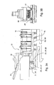
- each embodiment of the jack assembly includes a jack basic plastic part 14 and a jack plastic cover part 12.
- the plastic basic part 14 includes slots 16 for receiving wires such that they may electrically engage (terminate) with insulation displacement contacts 15.
- the jack plastic cover part 12 includes a plug opening 18 providing an RJ style interface with positioned spring contact conductors 21 - 28.
- the jack assembly 10 may be used individually or may be mounted in a bank with other similar jacks to provide a patch panel.
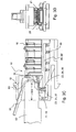
- the spring contact conductors 21 - 28 in the embodiment shown are provided in sets having different geometries.
- the outermost spring contacts 21 and 28 have a geometry that is more similar to known spring contact geometries but is preferably a bit longer.
- Each of the outermost spring contacts 21 and 28 terminate at a circuit board 66 (see Figures 3A and 3C), and then extend upwardly and then rearwardly (with respect to the plane of the plug opening 18) to a contact point or contact area 70.
- contacts 22, 24 and 26 have a shorter length and extend upwardly from the termination point (42, 44, 46) at the circuit board 66 and then extend rearwardly, at a different angle as compared to contacts 21 and 28.
- Contacts 23, 25 and 27 have a similar length to contacts 22, 24 and 26 but terminate (43, 45, 47) at the circuit board 66 rearwardly of the termination point of contacts 22, 24 and 26 .
- the spring contact conductors 21 - 28 each terminate at the printed circuit board 66.
- the different geometries allow the spring contact conductors 22 - 27 to terminate at different spacings from the circuit board termination location (or from a plane of the opening 18) while still providing a contact in the contact area 70. With this arrangement the spring contact conductors 21 - 28 engage corresponding conductor contacts 60 of an RJ plug 62 when the RJ plug 62 is inserted into a contact position.
- the RJ plug 62 plug is inserted into the opening 18 to assume a contact position.
- the plug contacts 60 extend a distance from the plane of the opening 18 to the contact position.
- the distance of the contacts 60 (and the contact area 70) from the plane of the opening 18, with the RJ plug 62 plug in the contact position is somewhat standard (within a tolerance range) and about 8.4mm.
- the RJ plug 62 plug has a latch element 63 that engages a surface of the jack plastic cover part 12 and seats the plug in the contact position. This maintains the set distance of the contacts 60 (and the plug contact area 70) from the plane of the opening 18.
- the plug contact area 70 for each of the spring contact conductors 21 - 28 is at about the same distance from the plane of the opening 18, even though there are three different geometries of the sets of spring contact conductors 21 - 28.
- the different geometries of the spring contact conductors 21 - 28 also lower or prevent crosstalk coupling of adjacent spring contact conductors 21 the 28 in regions outside the plug contact area 70.
- the respective termination location 41, 48 on the circuit board 66 for spring contact conductors 21 and 28 is much farther from contact area 70 and much closer to the plane of opening 18 as compared to the termination location for the spring contact conductors 22, 24, 26.
- the termination location along circuit board 66 for spring contact conductors 22, 24, 26 is closer to the plane of opening 18 as compared to the termination location for the spring contact conductors 23, 25 and 27.
- these termination locations provide different distances or signal paths from the termination location (41 - 48) to the contact area 70 (different conductive path lengths).
- the printed circuit board 66 ( Figures 4 and 5) has plated through holes 41 - 48 receiving respective spring contact conductors 21 - 28 to form the termination locations.
- the IDCs 15 connect to circuit boards 66 via plated through holes 81 -88.
- the plated through holes 41 - 48 are connected respectively to the respective plated through holes 81 -88 via interconnecting conductors in the form of traces 31 through 38.
- the plated through holes 41 - 48, the plated through holes 81 -88, and traces 31 through 38 continue the signal paths of the lines associated with spring contact conductors 21 - 28.
- the jack assembly 10 is used to provide communication lines for high-performance communication applications. Such transmission lines each include a pair of signal paths.
- the signal paths in the example include a pair of signal paths 1, 2 , a pair of signal paths 3, 6, a pair of signal paths 4, 5 and a pair of signal paths 7, 8.
- the signal paths 1, 2 are, in the region of the jack assembly 10, formed by the conductors including spring contact conductors 21, 22, plated through holes 41, 42, traces 31, 32 and IDC plated through holes 81, 82 and the connected IDCs 15. It can be seen that most of the signal paths of a pair for a line are adjacent to each other except for the region of signal paths 3, 6 involving the spring contact conductors 23 and 26.
- the spring contact conductors 23 and 26 are split, with spring contact conductors 24 and 25 being disposed between them.
- Spring contact conductors 25 and 24 are a center pair of conductors or center line conductors.
- Spring contact conductors 23 and 26 are a split pair of conductors or split line conductors. Crosstalk is problematic in this region with conductor 23 having conductor 22 from the 1, 2 transmission line on one side and conductor 24 from the numeral 4, 5 transmission line on the other side.
- Conductor 26 has conductor 24 from the 4, 5 transmission line on one side and conductor 27 from the 7, 8 transmission line on the other side.
- Conductive traces are also provided that do not provide paths of the line. Instead, a (dead end) trace of one line interacts with a (dead end) trace of another line to form a capacitor (more particularly a reactive element having capacitive and inductive aspects) referred to herein as a crosstalk compensating element.
- Figure 7 shows crosstalk compensating element 64 which includes traces connected to the termination location of spring contact conductor 24 and spring contact conductor 26.
- a compensating element 53 is provided which includes traces connected to the termination location of spring contact conductor 23 and spring contact conductor 25.
- Compensating element 53 introduces a compensating signal v 2 of a magnitude essentially equal to the magnitude of the crosstalk signal (noise signal) v 1 introduced between spring contact conductors 23 and 24 and the contact area 70.
- Compensating element 64 introduces a compensating signal V 2 of a magnitude essentially equal to the magnitude of the crosstalk signal (noise signal) v 1 introduced between the spring contact conductors 25 and 26 in the contact area 70.
- a first embodiment of the invention limits the compensation to a single compensation signal (single compensating element) such that ⁇ should not be more than 3.8 degrees. Otherwise, the resulting NEXT noise will not be acceptable (CAT 6 performance will not be attained). Applicant has also noticed that if the manufacturing tolerance is more than 14%, there is no apparent way to use a single compensation signal to reach the CAT6 performance requirements.
- the compensation signal takes a round way trip in the transmission line (using first signal path and second signal path of a transmission line)
- the real distance between v 1 and v 2 is usually less than 4.1 mm.
- the performance may be attained with a longer 6.2mm distance between v 1 and v 2 (between the contact region and the compensation element connection region).
- the jacks and jack assemblies 10 of the invention particularly provide a distance between contact point 70 of the plug and jack of one or more spring contact conductors 21- 28 to the application point of the compensation signal that is less than 6.2mm.
- the compensation signal is introduced or applied by one of the compensating elements (e.g.,35, 64) at a point such as the plated through hole 41 - 48 of the respective spring contact termination region.
- Figure 5 shows the terminated spring contact conductors 21 - 28, schematically illustrating the position of these conductors 21 - 28 in the contact state (the contact state is also shown in Figure 3).
- Figure 4A-4C show the lengths of the signal path from plug contact area 70 to termination location on the printed circuit board 66 (also 66'). From Figure 5 and 4A-4C it can be appreciated that the signal path length of the two sets of conductors 22, 24, 26 and 23, 25, 27 is shorter than the signal path length of a conductors 21 and 28. The shortened signal path length (including the length of the signal path through the curve) can be appreciated from Figures 4A-4C.
- the signal path length of a conductors 2land 28 is preferably longer than prior jacks.
- the signal path length of a conductors 2land 28 may also be shortened but this is not required to obtain the performance in the jack assembly according to the invention (crosstalk attenuation which must be reduced is significantly less than with the center conductors 24 and 25 and the split conductors 23 and 26). Particularly with the conductors 23, 24, 25 and 26 where crosstalk is more significant, the invention provides a shorter distance from the contact zone 70 to the termination location 43, 44, 45 and 46 of the respective conductors 23, 24, 25 and 26. Further, according to the invention, the compensation element 64 and compensation element 35 are applied to the termination location of the respective conductors 23, 24, 25 and 26.
- the signal path length of the respective conductors 23, 24, 25 and 26 is in each case less than 6.2mm.
- the distance from plug contact area 70, of the plug 62 and jack 10 for conductors 23, 25 and 27, is 5 mm. In the preferred embodiment illustrated, the distance from plug contact area 70, of the plug 62 and jack 10 for conductors 22, 24 and 26 is 4.2 mm.
- the termination area positioned differently provides a different spacing, providing a different signal path length. Also, the different geometries of adjacent conductors allows a lower coupling of adjacent conductors (reduces the initial crosstalk signal v 1 ), thereby requiring a lower compensating signal v 2 . Further, it is believed to be advantageous to provide equals path lengths for conductors 24 and 26 that are compensated by common compensating element 64.
- the cross talk affecting the split pair line (with spring contact conductors 23 and 26) from the left line (spring contact conductors 27 and 28) and from the right line (spring contact conductors 21 and 22) is also compensated.
- the right side pair first spring contact conductor 21 does not significantly affect the split pair first spring contact conductor 23.
- the right side pair second spring contact conductor 22 is adjacent to the split pair first spring contact conductor 23 such that there is signal coupling.
- the left side pair first spring contact conductor 27 is adjacent to the split pair second spring contact conductor 26 such that there is signal coupling.
- a third crosstalk compensation element 13 is connected to the circuit board 66 providing crosstalk compensation between the right side (third) transmission line first signal path (21, 41, 31) and the second transmission line first signal path (23, 43, 33) as the only crosstalk compensation applied between the third transmission line first signal path and second transmission line first signal path.
- a fourth crosstalk compensation element 68 is connected to the circuit board 66 providing crosstalk compensation between the left side (fourth) transmission line second signal path (28, 48, 38) and the second transmission line second signal path (26, 46, 36) as the only crosstalk compensation applied between the fourth transmission line second signal path and the second transmission line second signal path. Further, better performance may be provided (although it is not essential) by providing an impedance balancing element 62.
- the spring contacts 21 - 28 must still present the mechanical aspects required for a RJ 45 type connection.
- the allowable deflection of contact springs for a RJ 45 type connection must be taken into account.
- a spring contact (21 - 28) of a RJ45 connector can be viewed as a cantilever beam.
- the relation between the deflection and the beam length of a cantilever beam can be summarized as follows.
- ⁇ max 2 ⁇ ⁇ w ⁇ l 2 3 ⁇ E ⁇ h
- ⁇ max the allowable deflection without yield
- ⁇ w the allowable stress without yield
- I the distance between load and support
- E the Young's Modulus of the material
- h is the height of the beam section.
- Phosphorous copper is used for the spring contacts 21 - 28 as is commonly used for such electric connector springs. This has a value for E of about 110,000 N/mm 2 .
- ⁇ w is about 600 N/mm 2 .
- a conventional RJ45 contact spring has a cross section of 0.35mm in the height and 0.4mm in the width. When these are substituted into equation 6, one is provided with the relation of ⁇ max to l as depicted in Fig. 9.
- TIA/EIA 570 requires the RJ45 jacks to compatible with a 6 position RJ11 plug (see Figures 3A and 3B). It will add more 0.8mm deflection for pin 1 and pin 8 of RJ45 jack. So, the minimum required deflection for a RJ45 contact spring is about 1.5mm. It is clear from Figure 9 that with a conventional spring design the spring length would be no less than 10mm.
- the single-compensation-method is carried out using spring contacts 22 - 27 that have a shortened length from the contact area 70 to the termination location (42 - 47), namely to the cross talk compensation element (in the form of a single compensation).
- spring contacts 22 - 27 that have a shortened length from the contact area 70 to the termination location (42 - 47), namely to the cross talk compensation element (in the form of a single compensation).
- the performance requirements are met by providing spring contacts 22 - 27 that have a shortened length from the contact area 70 to the cross talk compensation element (in the form of a single compensation) whereas the spring contacts 21 and 28 (the pin1 signal path and the pin 8 signal path) have a longer path as compared to the other contact springs (pins) 22 - 27.
- the deflection requirements of TIA/EIA 570 is only applied to spring contacts 21 and 28 (pin 1 and pin 8) and this is met with the longer spring contacts 21 and 28.
- the spring contacts 22 - 27 have a thinner section as compared to the known cross section, namely with height of 0.3mm (with minor tolerance variation) and a width of 0.4 mm (or less with minor tolerance variation).
- a cross section with a height of 0.2 mm is used and a width of 0.4 mm (or less with minor tolerance variation).
- the contact force is also reduced.
- an insulated spring supporter 90 may be used to maintain the contact force.
- This connector 10 has a circuit board 66' that uses more than one compensation element for at least some of the paths (multi-phase compensation).
- Connector 10 presents hardware for 10G performance through 500MHz.
- a well-known crosstalk compensation scheme called multi-phase compensation can be used, providing a compensation phase between the same lines, in addition to the first phase, the technique discussed above. But, if the frequency band is too wide (so as to provide high throughput - bandwidth), the time delay of the compensation will make it difficult to balance the performances at both ends of the frequency band.
- the techniques as to spring contact length and termination relative to the contact zone 70 is also used for the first phase in the second embodiment for 10G performance and at least one second phase is also provided.
- V 1 is a vector representing the Near-End-Cross-Talk (NEXT) of the plug/jack, to compensate the noise (crosstalk)
- the well-known multi-phase compensation technique adds first compensation at some location after the crosstalk introduction point (in the vicinity of contact are 70) as an opposite signal vector V 2 .
- the signal V 2 has a magnitude that is about double the magnitude of the signal V 1 .
- a vector with the same polarity (involving the interaction of the same signal paths as the initial crosstalk noise) and magnitude of V 1 is added the same distance after V 2 to balance the time delay effect of V 2 .
- Fig. 10 depicts the concept.
- V x V 2 ⁇ sin ⁇ - V 1 ⁇ sin 2 ⁇ ⁇
- ⁇ 2 ⁇ ⁇ ⁇ l ⁇ f v
- l the length that the signal traveled and is equal to double of the distance between V 1 and V 2 .
- the v the signal transmission speed and f is the frequency.
- V res 4 ⁇ ⁇ 2 ⁇ l 2 ⁇ V 1 * f 2 - f t 2 v 2
- V res 0.
- V r ⁇ es V 1 ⁇ 4 ⁇ cos t ⁇ ⁇ - cos ⁇ 2 - 4 ⁇ t - 1 ⁇ cos ⁇ ( cos ⁇ t - cos ⁇ ) + t - 1 2
- A 4 ⁇ cos t ⁇ ⁇ - cos ⁇ 2 - 4 ⁇ t - 1 ⁇ cos ⁇ ( cos ⁇ t - cos ⁇ ) + t - 1 2
- TIA/EIA defines an augmented CAT6 cabling category for 10G Ethernet application that operates from 1MHz through 500MHz. A reasonable tuning frequency is 250MHz. Considering the residual noise of the lower end, 10MHz is the lowest frequency that TIA/EIA has defined as a test plug value. Taking a central test plug of the line 3, 6 pair and the line 4, 5 pair combination, the V 1 is -57dB from the de-embedded measurement. The allowable residual noise is -74dB by the TIA/EIA 568B.2-1 standard. When one substitutes this limit into equation 11, one gets A that must be no larger than 0.02.
- a circuit board 66' is shown that is deployed in the same manner as the circuit board 66 described above.
- the circuit board 66' of the second embodiment is connected with a plastic part 14 having slots 16 for insulation displacement contacts 15 and with a plastic cover part 12 ( see Figures 1 and 2).
- the circuit board 66' has spring contact conductors 21 through 28 that are terminated (connected to the circuit board traces) at termination locations 41 through 48 respectively.
- the termination locations are particularly plated through holes or using some other technique for connecting the spring contact to the traces of the circuit board.
- a circuit board such as 66' is used where communications are still based on multiple communication lines or transmission lines with each line based on a pair of signal paths.
- the signal paths (beginning and end of such paths carried by the circuit traces 31 - 38 on the circuit board 66') are labeled one (1) through eight (8).
- the termination locations 41 through 48 are connected with the respective interconnecting conductors or traces 31 through 38.
- the traces 31 through 38 continue the signal paths 1 through 8 of the transmission lines. Up to four transmission lines with paths 1 through 8 are associated with the spring contact conductors 21 - 28 through plated through holes or termination locations 41-48, traces 31 through 38 to plated through holes or termination locations 81 - 88 and respective insulation displacement contacts 15.
- the signal paths 1 and 2 are the outer left side transmission line and include the spring contacts 21 and 22, plated through holes 41 and 42, and 28, plated through holes 47 and 48, traces 37 and 38 are connected to respective IDCs 15 by plated through holes 87 and 88.
- the signal paths 4 and 5 are the center transmission line and include the spring contacts 24 and 25, plated through holes 44 and 45, and traces 34 and 35 connected to respective IDCs 15 by plated through holes 84 and 85.
- the signal paths 3 and 6 are the split pair transmission line and include the spring contacts 23 and 26, plated through holes 43 and 46, and traces 33 and 36 connected to respective IDCs 15 by plated through holes 83 and 86.
- the second embodiment of the invention compensates for crosstalk using what is sometimes referred to as multiphase compensation.
- a first compensation phase is provided with capacitors (reactive elements - compensation elements) such as 64 and 53 that introduce a signal from the signal paths not originally affected by the crosstalk that occurred near or at the plug contact area 70.
- the first compensation phase introduces a compensating signal V 2 .
- a second phase is applied (a second phase is not applied for each line and the center line and split pair line may have an uneven phase delay as noted) the signal V 2 . Is about twice the magnitude of the original crosstalk signal. If no second phase is applied between the lines, the single phase compensating signal of about the same value is introduced as noted above.
- the second phase of compensation reintroduces V 1 preferably at about the same spacing of V 2 from the original crosstalk value V 1 .
- V 2 or single phase is introduced into the signal paths less than 6.7 or 6.2 mm from the contact zone 70.
- a crosstalk compensation element (capacitor) 13 is connected to the circuit board 66 providing crosstalk compensation by applying the compensating signal between paths 1 and 3. This compensation element 13 is the only phase or first phase (but for different lines). As with the first embodiment an impedance balancing element 62 may be provided.
- At least one other compensation element 56 is provided introducing a compensating signal corresponding to V 1 which is based on interaction between the signal paths 5 and 6, signal paths originally affected by the crosstalk V 1 that occurred near or at the plug contact area 70.
- Compensation element 56 is connected in the range of 6.2 to 7.2 mm such as around 6.7mm from the termination locations 45, 46 providing advantages based on the application of compensating signal V 2 relative to compensating signal V 1 as noted above.
- two even phase delays may be employed between the three signal vectors, (i.e. the original (crosstalk), the 1 st compensation, and the 2nd compensation).
- an uneven phase delay is used to separate those signal vectors as only one set of paths has a second phase.
- the required balance compensation, (2nd compensation) is tiny.
- the final result should be little affected by the phase delay error of this tiny signal.
- the compensation element 56 may also be applied so as to provide a larger phase delay and hence a smaller compensation magnitude. With this, and considering the area required by compensation circuits, the 2nd compensation (the compensation element 56) may be far away from the 1 st compensation (64, 53).
- the 2nd compensation in the form of the compensation element 56 deployed as an uneven phase delay may be connected to termination locations 85, 86 to provide good 10G performance (TIA/EIA augmented CAT6 cabling category for 10G Ethernet application that operate from 1MHz through 500MHz).
Abstract
Description
- The present invention relates to electrical connectors such as RJ style plug and jack connectors for communications systems and more particularly to such connectors which attain a high level of throughput transmission performance such as TIA (Telecommunications Industry Association) /EIA (Electronic Industries Alliance) category six performance (CAT 6).
- The increasing Internet traffic and the increased complexity and use of web applications has forced network providers and network infrastructure managers to seek enhanced transmission speeds for network equipment. The TIA/EIA set up a high-performance cabling category to fulfill this requirement often referred to as CAT 6.
- Such high-performance cabling uses a format with
RJ 45 jacks and plugs. The agreed to format for the lines at such a connector involves a line with a center pair of conductors at the connector and a split pair of conductors at the connector. One conductor contact of the split pair is on each side of the center pair conductor contacts. When such an RJ45 plug mates with anRJ 45 jack with signals at such high frequencies (as per the standard), the split pair will suffer a significant Near End Cross Talk (NEXT) problem from the other pairs. - It is known that electrical signals of one pair of conductors may be coupled onto the other pair of conductors for compensating or canceling crosstalk.
JP 64 [1989] 20690 -
United States Patent 5,997,358 (US '358) discloses an electrical connector that achieves high transmission performance (CAT 6) by providing compensation stages for introducing predetermined amounts of compensation between pairs of conductors. Two or more of such compensation stages are provided. A first compensation stage adds a compensation signal that is time delayed with respect to the other compensation stages. In the first stage, compensating crosstalk is introduced between the pairs of a first predetermined magnitude and phase in a given frequency. In a second stage, compensating crosstalk is introduced between pairs that has a second magnitude and phase at a given frequency. The first stage magnitude is larger than the offending crosstalk and the second stage reintroduces the offending crosstalk. Multiple compensation stages may be used to compensate for a phase issues, because, at high frequencies, compensating crosstalk cannot be introduced that is exactly 180° out of phase with the offending crosstalk. - It is an object of the invention to provide a connector jack that includes spring contacts with conductor pairs for plural lines defining an RJ style contact interface for connection with an RJ style plug, and with interconnecting circuitry on a printed circuit board, and with crosstalk compensation provided to achieve high levels of throughput.
- According to the invention, an electrical connector is provided comprising a circuit board with interconnecting conductors respectively extending between spring contact termination locations and other termination locations. A set of spring contact conductors is provided, each terminating at a respective one of the spring contact termination locations. Each of the spring contact conductors of the set of spring contact conductors has a plug contact zone and defines a spring contact conductive path from an associated plug contact zone to a respective spring contact termination location that is 6.7mm or less, or even 6.2mm or less.
- An additional set of spring contact conductors may be provided, each terminating at a respective one of the spring contact termination locations. This additional set of spring contact conductors includes a right outside spring contact conductor on a right side of the other set of spring contact conductors and left outside spring contact conductor on a left side of the other set of spring contact conductors. The additional set of spring contact conductors may each have a plug contact zone and define a spring contact conductive path from an associated plug contact zone to a respective spring
contact termination location 10 mm or greater. This allows a spring contact (pin) configuration that achieves physical requirements for jack and plug connection. - The spring contact termination locations may be offset with adjacent spring contact termination locations being differently spaced from the plug contact zone, with some of the first set of spring contact conductors having a spring contact conductive path that is from 4.8 mm to 5.2 mm and others of the first set of spring contact conductors having a spring contact conductive path that is from 4.0 mm to 4.4 mm.
- The pairs of interconnecting conductors and electrically connected spring contact conductors form part of transmission lines. The connector advantageously further comprises a first/second crosstalk compensation element providing a crosstalk compensation signal between a first interconnecting conductor of one line and a second interconnecting conductor of another line and a second/first crosstalk compensation element providing a crosstalk compensation signal between a second interconnecting conductor of the one line and a first interconnecting conductor of the another line, with each crosstalk compensation element being applied at or closely adjacent to the termination location. The first/second crosstalk compensation element and the second/first crosstalk compensation element may be the only compensation element connected between the first line and the second line on the circuit board. Another crosstalk compensation element may provide a crosstalk compensation signal between an interconnecting conductor of one line and an interconnecting conductor of the second line. The another crosstalk compensation element providing a further crosstalk compensation signal may be applied less than 7.2mm, or less than 6.7mm or 6.2mm, from a termination location of the one line and the second line or at the opposite termination location (IDC termination location).
- It is a further object of the invention to provide a connector jack that includes a center spring contact conductor pair (of a first transmission line) and a split pair of spring contact conductors (of a second transmission line), with one conductor on each side of the center spring contact conductor pair, with the conductors defining an RJ style contact interface and with interconnecting circuitry such as a printed circuit board which is simplified so as to only have a single crosstalk compensation element (providing a compensation signal) for each source of crosstalk, wherein signals carried by the first transmission line and the second transmission line following the compensation elements is no more than -46dB at 250MZ.
- According to another aspect of the invention an electrical connector jack is provided with a body with a support portion and a plug receiving portion defining an opening with an insertion plane and a circuit board mounted to the support portion to position the circuit board relative to the plug receiving insertion plane. The circuit board has circuit traces respectively extending from the spring contact termination locations. The spring contact termination locations include a first set of spring contact termination locations spaced a first distance from the insertion plane, a second set of spring contact termination locations spaced a second distance from the insertion plane, and a third set of spring contact termination locations spaced a third distance from the insertion plane. A plurality of spring contact conductors, each terminating at a respective one of the spring contact termination locations, are provided having a common plug contact zone. The common plug contact zone is spaced substantially a common distance from the insertion plane.
- Each of the spring contact conductors provides a conductive path from the plug contact zone to a respective spring contact termination location. The spring contact conductors connected to the first set of spring contact termination locations and the second set of spring contact termination locations may advantageously have a conductive path that is 7 mm or less, and the spring contact conductors connected to the third set of spring contact termination locations may advantageously have a conductive path that is 7 mm or greater.
- The various features of novelty which characterize the invention are pointed out with particularity in the claims annexed to and forming a part of this disclosure. For a better understanding of the invention, its operating advantages and specific objects attained by its uses, reference is made to the accompanying drawings and descriptive matter in which preferred embodiments of the invention are illustrated.
- In the drawings:
- Figure 1 is a perspective view of a jack assembly according to a first and second embodiment according to the invention;
- Figure 2 is a perspective view showing the jack of Figure 1 with a jack cover part removed;
- Figure 3A is a partially sectional side view showing the jack assembly of Figure 1 mated with a six contact RJ plug;
- Figure 3B is a sectional end view showing the jack assembly of Figure 1 taken through a six contact RJ plug in a mated position;
- Figure 3C is a partially sectional and cut side away view showing the jack assembly of Figure 1 mated with an eight contact RJ plug;
- Figure 3D is a sectional end view showing the jack assembly of Figure 1 taken through an eight contact RJ plug in a mated position;
- Figure 4A is a sectional view through a circuit board showing a spring contact of a set of spring contacts and showing the signal path length from a contact area to a termination location on the printed circuit board;
- Figure 4B is a sectional view through the circuit board showing a spring contact of a set of spring contacts and showing the signal path length from a contact area to a termination location on the printed circuit board;
- Figure 4C is a sectional view through the circuit board showing a spring contact of a set of spring contacts and showing the signal path length from a contact area to a termination location on the printed circuit board;
- Figure 5 is a perspective view showing the jack assembly of Figure 1 mated with an eight contact RJ plug shown in phantom line and showing a distance from the contact zone to the plane of the opening of the jack;
- Figure 6 is an explanatory diagram view from the complex plane illustrating aspects of crosstalk compensation for a first or only compensation phase of a first and second embodiment according to the invention;
- Figure 7 is a view of a first side of a circuit board according to a first embodiment of the jack assembly of Figure 1;
- Figure 8 is a view of a second side of a circuit board of Figure 7;
- Figure 9 is a view showing the normal relationship between spring contact deflection and spring contact length;
- Figure 10 is an explanatory diagram illustrating aspects of crosstalk compensation for first or and second compensation phases according to a second embodiment of the invention;
- Figure 11 is a view of a first side of a circuit board of the second embodiment of of the jack assembly of Figure 1; and
- Figure 12 is a view of a second side of a circuit board of Figure 11.
- Referring to the drawings in particular, Figure 1 shows a jack assembly generally designated 10. The
jack assembly 10 may be provided in one of several embodiments as discussed below. The difference between the different embodiments relates to different circuit board embodiments, as discussed below. Otherwise, each embodiment of the jack assembly includes a jack basicplastic part 14 and a jackplastic cover part 12. The plasticbasic part 14 includesslots 16 for receiving wires such that they may electrically engage (terminate) withinsulation displacement contacts 15. The jackplastic cover part 12 includes aplug opening 18 providing an RJ style interface with positioned spring contact conductors 21 - 28. Thejack assembly 10 may be used individually or may be mounted in a bank with other similar jacks to provide a patch panel. - The spring contact conductors 21 - 28 in the embodiment shown are provided in sets having different geometries. The
outermost spring contacts outermost spring contacts contact area 70. As can be seen in Figures 4A, 4B and 4C,contacts circuit board 66 and then extend rearwardly, at a different angle as compared tocontacts Contacts contacts circuit board 66 rearwardly of the termination point ofcontacts circuit board 66. The different geometries allow the spring contact conductors 22 - 27 to terminate at different spacings from the circuit board termination location (or from a plane of the opening 18) while still providing a contact in thecontact area 70. With this arrangement the spring contact conductors 21 - 28 engage correspondingconductor contacts 60 of anRJ plug 62 when the RJ plug 62 is inserted into a contact position. - As shown in Figure 3A-3D, the RJ plug 62 plug is inserted into the
opening 18 to assume a contact position. In this contact position theplug contacts 60 extend a distance from the plane of theopening 18 to the contact position. The distance of the contacts 60 (and the contact area 70) from the plane of theopening 18, with the RJ plug 62 plug in the contact position, is somewhat standard (within a tolerance range) and about 8.4mm. Typically the RJ plug 62 plug has alatch element 63 that engages a surface of the jackplastic cover part 12 and seats the plug in the contact position. This maintains the set distance of the contacts 60 (and the plug contact area 70) from the plane of theopening 18. Theplug contact area 70 for each of the spring contact conductors 21 - 28 is at about the same distance from the plane of theopening 18, even though there are three different geometries of the sets of spring contact conductors 21 - 28. The different geometries of the spring contact conductors 21 - 28 also lower or prevent crosstalk coupling of adjacentspring contact conductors 21 the 28 in regions outside theplug contact area 70. - As can be seen in Figures 7 and 8 the
respective termination location circuit board 66 forspring contact conductors contact area 70 and much closer to the plane of opening 18 as compared to the termination location for thespring contact conductors circuit board 66 forspring contact conductors spring contact conductors - The printed circuit board 66 (Figures 4 and 5) has plated through holes 41 - 48 receiving respective spring contact conductors 21 - 28 to form the termination locations. The
IDCs 15 connect tocircuit boards 66 via plated through holes 81 -88. The plated through holes 41 - 48 are connected respectively to the respective plated through holes 81 -88 via interconnecting conductors in the form oftraces 31 through 38. The plated through holes 41 - 48, the plated through holes 81 -88, and traces 31 through 38 continue the signal paths of the lines associated with spring contact conductors 21 - 28. - The
jack assembly 10 is used to provide communication lines for high-performance communication applications. Such transmission lines each include a pair of signal paths. The signal paths in the example include a pair ofsignal paths signal paths 3, 6, a pair ofsignal paths signal paths signal paths jack assembly 10, formed by the conductors includingspring contact conductors holes holes connected IDCs 15. It can be seen that most of the signal paths of a pair for a line are adjacent to each other except for the region ofsignal paths 3, 6 involving thespring contact conductors spring contact conductors spring contact conductors Spring contact conductors Spring contact conductors conductor 23 havingconductor 22 from the 1, 2 transmission line on one side andconductor 24 from thenumeral Conductor 26 hasconductor 24 from the 4, 5 transmission line on one side andconductor 27 from the 7, 8 transmission line on the other side. - Conductive traces are also provided that do not provide paths of the line. Instead, a (dead end) trace of one line interacts with a (dead end) trace of another line to form a capacitor (more particularly a reactive element having capacitive and inductive aspects) referred to herein as a crosstalk compensating element. Figure 7 shows
crosstalk compensating element 64 which includes traces connected to the termination location ofspring contact conductor 24 andspring contact conductor 26. A compensatingelement 53 is provided which includes traces connected to the termination location ofspring contact conductor 23 andspring contact conductor 25. Compensatingelement 53 introduces a compensating signal v2 of a magnitude essentially equal to the magnitude of the crosstalk signal (noise signal) v1 introduced betweenspring contact conductors contact area 70. Compensatingelement 64 introduces a compensating signal V2 of a magnitude essentially equal to the magnitude of the crosstalk signal (noise signal) v1 introduced between thespring contact conductors contact area 70. - As shown on the Figure 6, to compensate the noise v1, a signal v2 is added a distance after (along the signal path) the point or region of application of v1 (the contact region 70). Considering the view from the complex plane (Figure 6), this distance will revel a phase delay denoted ϕ in Figure 6. From Figure 6 one can see that the vector sum of v1 and v2 will result in a vector vt with two components as follows:


when v2 = v1 cos ϕ. Hence:


- A first embodiment of the invention limits the compensation to a single compensation signal (single compensating element) such that ϕ should not be more than 3.8 degrees. Otherwise, the resulting NEXT noise will not be acceptable (CAT 6 performance will not be attained). Applicant has also noticed that if the manufacturing tolerance is more than 14%, there is no apparent way to use a single compensation signal to reach the CAT6 performance requirements.
- When considering the electromagnetic waves propagated in the transmission line made of copper, one can use a usual speed factor of 0.65. The wavelength at 250MHz will be 0.78meter. As such the physical length related to a 3.8 degree phase delay is 8.2 mm. However, because the compensation signal takes a round way trip in the transmission line (using first signal path and second signal path of a transmission line), the real distance between v1 and v2 (between the contact region and the compensation element connection region) is usually less than 4.1 mm. With a 10% manufacturing tolerance, that is at the boundary of today's manufacturing technical abilities, the performance may be attained with a longer 6.2mm distance between v1 and v2 (between the contact region and the compensation element connection region). The jacks and
jack assemblies 10 of the invention particularly provide a distance betweencontact point 70 of the plug and jack of one or more spring contact conductors 21- 28 to the application point of the compensation signal that is less than 6.2mm. The compensation signal is introduced or applied by one of the compensating elements (e.g.,35, 64) at a point such as the plated through hole 41 - 48 of the respective spring contact termination region. - Figure 5 shows the terminated spring contact conductors 21 - 28, schematically illustrating the position of these conductors 21 - 28 in the contact state (the contact state is also shown in Figure 3). Figure 4A-4C show the lengths of the signal path from
plug contact area 70 to termination location on the printed circuit board 66 (also 66'). From Figure 5 and 4A-4C it can be appreciated that the signal path length of the two sets ofconductors conductors center conductors split conductors 23 and 26). Particularly with theconductors contact zone 70 to thetermination location respective conductors compensation element 64 andcompensation element 35 are applied to the termination location of therespective conductors respective conductors plug contact area 70, of theplug 62 andjack 10 forconductors plug contact area 70, of theplug 62 andjack 10 forconductors conductors element 64. Likewise it is believed to be advantageous to provide equal path lengths forconductors element 35. Further, as noted, it is unnecessary to provide a shortened signal path length for theouter conductors 21 and 28 (according to the disclosed embodiment). As such, the costs involved in providing the shorter and more precise conductors 22 - 27 can be avoided in the case ofspring contact conductors - The cross talk affecting the split pair line (with
spring contact conductors 23 and 26) from the left line (spring contact conductors 27 and 28) and from the right line (spring contact conductors 21 and 22) is also compensated. The right side pair firstspring contact conductor 21 does not significantly affect the split pair firstspring contact conductor 23. However, the right side pair secondspring contact conductor 22 is adjacent to the split pair firstspring contact conductor 23 such that there is signal coupling. The left side pair firstspring contact conductor 27 is adjacent to the split pair secondspring contact conductor 26 such that there is signal coupling. A thirdcrosstalk compensation element 13 is connected to thecircuit board 66 providing crosstalk compensation between the right side (third) transmission line first signal path (21, 41, 31) and the second transmission line first signal path (23, 43, 33) as the only crosstalk compensation applied between the third transmission line first signal path and second transmission line first signal path. A fourthcrosstalk compensation element 68 is connected to thecircuit board 66 providing crosstalk compensation between the left side (fourth) transmission line second signal path (28, 48, 38) and the second transmission line second signal path (26, 46, 36) as the only crosstalk compensation applied between the fourth transmission line second signal path and the second transmission line second signal path. Further, better performance may be provided (although it is not essential) by providing animpedance balancing element 62. - To implement the single compensation system of the invention, the spring contacts 21 - 28 must still present the mechanical aspects required for a
RJ 45 type connection. The allowable deflection of contact springs for aRJ 45 type connection must be taken into account. - A spring contact (21 - 28) of a RJ45 connector can be viewed as a cantilever beam. The relation between the deflection and the beam length of a cantilever beam can be summarized as follows.

where
δ max is the allowable deflection without yield,
σ w is the allowable stress without yield,
I is the distance between load and support,
E is the Young's Modulus of the material,
h is the height of the beam section.
Phosphorous copper is used for the spring contacts 21 - 28 as is commonly used for such electric connector springs. This has a value for E of about 110,000 N/mm2. The value of σw is about 600 N/mm2. A conventional RJ45 contact spring has a cross section of 0.35mm in the height and 0.4mm in the width. When these are substituted into equation 6, one is provided with the relation of δmax to l as depicted in Fig. 9. - From Fig. 9, it can be appreciated that for the spring length less than 7mm, the allowable deflection of the spring is less than 0.5mm. The FCC Part68 requires a 0.3mm tolerance for the deflection of the spring to cover the tolerance of heights of Plug blades. Manufacturing issues provide for another 0.3mm deflection tolerance for production errors. To make the problem more complex, TIA/EIA 570 requires the RJ45 jacks to compatible with a 6 position RJ11 plug (see Figures 3A and 3B). It will add more 0.8mm deflection for
pin 1 andpin 8 of RJ45 jack. So, the minimum required deflection for a RJ45 contact spring is about 1.5mm. It is clear from Figure 9 that with a conventional spring design the spring length would be no less than 10mm. - According to the invention, the single-compensation-method is carried out using spring contacts 22 - 27 that have a shortened length from the
contact area 70 to the termination location (42 - 47), namely to the cross talk compensation element (in the form of a single compensation). However, as indicated above, to reach a higher performance for new performance requirements with a conventional design there is no way to shorten the length of the spring and fulfill the requirement of its deflection imposed by the FCC and TIA/EIA 570 as noted above. According to the invention, the performance requirements are met by providing spring contacts 22 - 27 that have a shortened length from thecontact area 70 to the cross talk compensation element (in the form of a single compensation) whereas thespring contacts 21 and 28 (the pin1 signal path and thepin 8 signal path) have a longer path as compared to the other contact springs (pins) 22 - 27. With this the deflection requirements of TIA/EIA 570 is only applied tospring contacts 21 and 28 (pin 1 and pin 8) and this is met with thelonger spring contacts insulated spring supporter 90 may be used to maintain the contact force. - Another embodiment of the invention is described with reference to Figures 10 through 12. This
connector 10 has a circuit board 66' that uses more than one compensation element for at least some of the paths (multi-phase compensation).Connector 10 presents hardware for 10G performance through 500MHz. To design a connector for high frequency and high performance, a well-known crosstalk compensation scheme called multi-phase compensation can be used, providing a compensation phase between the same lines, in addition to the first phase, the technique discussed above. But, if the frequency band is too wide (so as to provide high throughput - bandwidth), the time delay of the compensation will make it difficult to balance the performances at both ends of the frequency band. The techniques as to spring contact length and termination relative to thecontact zone 70 is also used for the first phase in the second embodiment for 10G performance and at least one second phase is also provided. - If V1 is a vector representing the Near-End-Cross-Talk (NEXT) of the plug/jack, to compensate the noise (crosstalk), the well-known multi-phase compensation technique adds first compensation at some location after the crosstalk introduction point (in the vicinity of contact are 70) as an opposite signal vector V2. The signal V2 has a magnitude that is about double the magnitude of the signal V1. Then a vector with the same polarity (involving the interaction of the same signal paths as the initial crosstalk noise) and magnitude of V1 is added the same distance after V2 to balance the time delay effect of V2. Fig. 10 depicts the concept. One may calculate the vector sum as:


- The rule of thumb is to make the residual vector Vres zero at the middle of the bandwidth so that the performance will be symmetrically balanced for both ends. The frequency where the NEXT is made zero is called tuned frequency. Hence, one knows that at the tuned
frequency 
equation 7 provides the residual noise associated with any frequency.


equation 8 one will get

- Manufacturing tolerances may next be considered. In order to make the calculation easier to understand, an error may be assigned to the original vector.


equation 10 one gets

- Taking into consideration real world factors, TIA/EIA defines an augmented CAT6 cabling category for 10G Ethernet application that operates from 1MHz through 500MHz. A reasonable tuning frequency is 250MHz. Considering the residual noise of the lower end, 10MHz is the lowest frequency that TIA/EIA has defined as a test plug value. Taking a central test plug of the
line 3, 6 pair and theline equation 10, one has 3792l2 + 16l2 - 0.03 ≤ 0. This results in l ≤ 13.4, and the distance between V1 and V2 has to be less than 6.7mm, namely the distance fromcontact zone 70 to the termination location, which is the distance from the crosstalk signal to the location the first compensation. - Referring to Figure 11 and 12, a circuit board 66' is shown that is deployed in the same manner as the
circuit board 66 described above. Particularly, the circuit board 66' of the second embodiment is connected with aplastic part 14 havingslots 16 forinsulation displacement contacts 15 and with a plastic cover part 12 ( see Figures 1 and 2). The circuit board 66' hasspring contact conductors 21 through 28 that are terminated (connected to the circuit board traces) attermination locations 41 through 48 respectively. The termination locations are particularly plated through holes or using some other technique for connecting the spring contact to the traces of the circuit board. - With higher throughput applications (10 G) using a
jack assembly 10, a circuit board such as 66' is used where communications are still based on multiple communication lines or transmission lines with each line based on a pair of signal paths. In Figures 10 and 11 the signal paths (beginning and end of such paths carried by the circuit traces 31 - 38 on the circuit board 66') are labeled one (1) through eight (8). Thetermination locations 41 through 48 are connected with the respective interconnecting conductors or traces 31 through 38. Thetraces 31 through 38 continue thesignal paths 1 through 8 of the transmission lines. Up to four transmission lines withpaths 1 through 8 are associated with the spring contact conductors 21 - 28 through plated through holes or termination locations 41-48, traces 31 through 38 to plated through holes or termination locations 81 - 88 and respectiveinsulation displacement contacts 15. - The
signal paths spring contacts holes holes 47 and 48, traces 37 and 38 are connected torespective IDCs 15 by plated throughholes signal paths spring contacts holes respective IDCs 15 by plated throughholes signal paths 3 and 6 are the split pair transmission line and include thespring contacts holes respective IDCs 15 by plated throughholes - The second embodiment of the invention compensates for crosstalk using what is sometimes referred to as multiphase compensation. A first compensation phase is provided with capacitors (reactive elements - compensation elements) such as 64 and 53 that introduce a signal from the signal paths not originally affected by the crosstalk that occurred near or at the
plug contact area 70. The first compensation phase introduces a compensating signal V2. Where a second phase is applied (a second phase is not applied for each line and the center line and split pair line may have an uneven phase delay as noted) the signal V2. Is about twice the magnitude of the original crosstalk signal. If no second phase is applied between the lines, the single phase compensating signal of about the same value is introduced as noted above. The second phase of compensation reintroduces V1 preferably at about the same spacing of V2 from the original crosstalk value V1 . Because thecompensation elements termination locations contact zone 70. A crosstalk compensation element (capacitor) 13 is connected to thecircuit board 66 providing crosstalk compensation by applying the compensating signal betweenpaths compensation element 13 is the only phase or first phase (but for different lines). As with the first embodiment animpedance balancing element 62 may be provided. - To achieve greater bandwidth (higher throughput) at least one
other compensation element 56 is provided introducing a compensating signal corresponding to V1 which is based on interaction between thesignal paths 5 and 6, signal paths originally affected by the crosstalk V1 that occurred near or at theplug contact area 70.Compensation element 56 is connected in the range of 6.2 to 7.2 mm such as around 6.7mm from thetermination locations compensation element 56 may also be applied so as to provide a larger phase delay and hence a smaller compensation magnitude. With this, and considering the area required by compensation circuits, the 2nd compensation (the compensation element 56) may be far away from the 1 st compensation (64, 53). For example with V2 (the first compensation phase) applied by thecompensation elements compensation element 56 deployed as an uneven phase delay may be connected totermination locations - While specific embodiments of the invention have been shown and described in detail to illustrate the application of the principles of the invention, it will be understood that the invention may be embodied otherwise without departing from such principles.
Claims (7)
- An electrical connector jack comprising:a body with a support portion and a plug receiving portion defining an opening with an insertion plane;a circuit board mounted to said support portion to position said circuit board relative to said plug receiving said insertion plane, said circuit board having circuit traces respectively extending from said spring contact termination locations, said spring contact termination locations including a first set of spring contact termination locations spaced a first distance from said insertion plane, a second set of spring contact termination locations spaced a second distance from said insertion plane and a third set of spring contact termination locations spaced a third distance from said insertion plane; anda plurality of spring contact conductors each terminating at a respective one of said spring contact termination locations, each of said spring contact conductors having a common plug contact zone spaced substantially at a common distance from said insertion plane.
- An electrical connector jack according to claim 1, wherein each of said spring contact conductors provides a conductive path from said plug contact zone to a respective said spring contact termination location and spring contact conductors connected to said first set of spring contact termination locations and said second set of spring contact termination locations have a conductive path that is 7 mm or less and spring contact conductors connected to said third set of spring contact termination locations have a conductive path that is 7 mm or greater.
- An electrical connector jack according to claim 2, wherein each of said spring contact conductors provides a conductive path from said plug contact zone to a respective said spring contact termination location and said spring contact conductors connected to said first set of spring contact termination locations have a conductive path that is between 4 and 5 mm and said second set of spring contact termination locations have a conductive path that is between 4.5 mm and 5.5 mm and said spring contact conductors connected to said third set of spring contact termination locations have a conductive path that is 10 mm or greater.
- An electrical connector jack according to claim 2, wherein each of said spring contact conductors provides a conductive path from said plug contact zone to a respective said spring contact termination location and spring contact conductors connected to said first set of spring contact termination locations and said second set of spring contact termination locations have a cross section with height of less than 0.35 mm or less and a width of 0.4 mm or less.
- An electrical connector jack according to claim 2, wherein each of said spring contact conductors provides a conductive path from said plug contact zone to a respective said spring contact termination location and spring contact conductors connected to said first set of spring contact termination locations and said second set of spring contact termination locations have a minimum deflection less than 1.5 mm and spring contact conductors connected to said third set of spring contact termination locations have a minimum deflection of at least 1.5 mm.
- An electrical connector jack according to claim 1, wherein each of said spring contact conductors provides a conductive path from a plug contact zone to a respective said spring contact termination location and three spring contact conductors are connected to said first set of spring contact termination locations and three said spring contact conductors are connected to said second set of spring contact termination locations with spring contact conductors connected to said first set of spring contact termination locations alternating with spring contact conductors connected to said second set of spring contact termination locations to provide contacts of alternating termination and two spring contact conductors are connected to said third set of spring contact termination locations with one of said spring contact conductors connected to said third set of spring contact termination locations extending on one side of said contacts of alternating termination and another of said spring contact conductors connected to said third set of spring contact termination locations extending on another side of said contacts of alternating termination.
- An electrical connector jack according to claim 6, wherein a cross section of said contacts of alternating termination is smaller than a cross section of said spring contact conductors connected to said third set of spring contact termination locations.
Applications Claiming Priority (2)
| Application Number | Priority Date | Filing Date | Title |
|---|---|---|---|
| US11/360,101 US20070197102A1 (en) | 2006-02-23 | 2006-02-23 | Connector for communications systems having category 6 performance using a single compensation signal or higher performance using plural compensation signals |
| US11/369,257 US7367849B2 (en) | 2006-03-07 | 2006-03-07 | Electrical connector with shortened contact and crosstalk compensation |
Publications (2)
| Publication Number | Publication Date |
|---|---|
| EP1826879A1 true EP1826879A1 (en) | 2007-08-29 |
| EP1826879B1 EP1826879B1 (en) | 2011-12-21 |
Family
ID=37907145
Family Applications (1)
| Application Number | Title | Priority Date | Filing Date |
|---|---|---|---|
| EP06013783A Active EP1826879B1 (en) | 2006-02-23 | 2006-07-04 | Connector for communications systems having contact pin arrangement and crosstalk compensation means for improved performance |
Country Status (6)
| Country | Link |
|---|---|
| EP (1) | EP1826879B1 (en) |
| JP (1) | JP4879694B2 (en) |
| AT (1) | ATE538517T1 (en) |
| AU (1) | AU2006202309B2 (en) |
| CA (1) | CA2549918C (en) |
| DK (1) | DK1826879T3 (en) |
Cited By (5)
| Publication number | Priority date | Publication date | Assignee | Title |
|---|---|---|---|---|
| US7828603B1 (en) | 2010-01-07 | 2010-11-09 | Yfc-Boneagle Electric Co., Ltd. | Electrical connector with crosstalk compensation |
| GB2452002B (en) * | 2006-05-17 | 2011-03-09 | Tyco Electronics Corp | Electrical connecter having staggered contacts |
| WO2011056491A1 (en) * | 2009-11-03 | 2011-05-12 | Panduit Corp. | Communication connector with improved crosstalk compensation |
| EP2363925A1 (en) * | 2010-01-11 | 2011-09-07 | YFC-Boneagle Electric Co., Ltd. | Electrical connector with crosstalk compensation |
| WO2020160275A1 (en) * | 2019-01-31 | 2020-08-06 | Commscope Technologies Llc | Anti-arc connector and pin array for a port |
Families Citing this family (2)
| Publication number | Priority date | Publication date | Assignee | Title |
|---|---|---|---|---|
| US8167661B2 (en) * | 2008-12-02 | 2012-05-01 | Panduit Corp. | Method and system for improving crosstalk attenuation within a plug/jack connection and between nearby plug/jack combinations |
| CA2647704A1 (en) | 2008-12-22 | 2010-06-22 | Belden Cdt (Canada) Inc. | Coupler connector |
Citations (6)
| Publication number | Priority date | Publication date | Assignee | Title |
|---|---|---|---|---|
| US6089923A (en) * | 1999-08-20 | 2000-07-18 | Adc Telecommunications, Inc. | Jack including crosstalk compensation for printed circuit board |
| WO2002015345A1 (en) * | 2000-08-10 | 2002-02-21 | Legrand | Modular connector |
| US6464541B1 (en) * | 2001-05-23 | 2002-10-15 | Avaya Technology Corp. | Simultaneous near-end and far-end crosstalk compensation in a communication connector |
| EP1365486A1 (en) * | 2002-05-21 | 2003-11-26 | Hirose Electric Co., Ltd. | Modular jack connector |
| GB2393858A (en) * | 2002-10-03 | 2004-04-07 | Brand Rex Ltd | High-frequency socket connector |
| US20040102097A1 (en) * | 2002-11-22 | 2004-05-27 | Clark Gordon P. | Telecommunications jack assembly |
Family Cites Families (3)
| Publication number | Priority date | Publication date | Assignee | Title |
|---|---|---|---|---|
| US6186834B1 (en) * | 1999-06-08 | 2001-02-13 | Avaya Technology Corp. | Enhanced communication connector assembly with crosstalk compensation |
| JP4495304B2 (en) * | 2000-05-26 | 2010-07-07 | パナソニック電工株式会社 | Modular jack |
| JP4026524B2 (en) * | 2003-03-26 | 2007-12-26 | 松下電工株式会社 | Modular connector |
-
2006
- 2006-05-30 AU AU2006202309A patent/AU2006202309B2/en active Active
- 2006-06-09 CA CA2549918A patent/CA2549918C/en active Active
- 2006-07-04 AT AT06013783T patent/ATE538517T1/en active
- 2006-07-04 DK DK06013783.3T patent/DK1826879T3/en active
- 2006-07-04 EP EP06013783A patent/EP1826879B1/en active Active
- 2006-10-03 JP JP2006271393A patent/JP4879694B2/en not_active Expired - Fee Related
Patent Citations (6)
| Publication number | Priority date | Publication date | Assignee | Title |
|---|---|---|---|---|
| US6089923A (en) * | 1999-08-20 | 2000-07-18 | Adc Telecommunications, Inc. | Jack including crosstalk compensation for printed circuit board |
| WO2002015345A1 (en) * | 2000-08-10 | 2002-02-21 | Legrand | Modular connector |
| US6464541B1 (en) * | 2001-05-23 | 2002-10-15 | Avaya Technology Corp. | Simultaneous near-end and far-end crosstalk compensation in a communication connector |
| EP1365486A1 (en) * | 2002-05-21 | 2003-11-26 | Hirose Electric Co., Ltd. | Modular jack connector |
| GB2393858A (en) * | 2002-10-03 | 2004-04-07 | Brand Rex Ltd | High-frequency socket connector |
| US20040102097A1 (en) * | 2002-11-22 | 2004-05-27 | Clark Gordon P. | Telecommunications jack assembly |
Cited By (12)
| Publication number | Priority date | Publication date | Assignee | Title |
|---|---|---|---|---|
| GB2452002B (en) * | 2006-05-17 | 2011-03-09 | Tyco Electronics Corp | Electrical connecter having staggered contacts |
| WO2011056491A1 (en) * | 2009-11-03 | 2011-05-12 | Panduit Corp. | Communication connector with improved crosstalk compensation |
| US7985103B2 (en) | 2009-11-03 | 2011-07-26 | Panduit Corp. | Communication connector with improved crosstalk communication |
| US8052483B1 (en) | 2009-11-03 | 2011-11-08 | Panduit Corp. | Communication connector with improved crosstalk connection |
| US8182295B2 (en) | 2009-11-03 | 2012-05-22 | Panduit Corp. | Communication connector with improved crosstalk compensation |
| US8303348B2 (en) | 2009-11-03 | 2012-11-06 | Panduit Corp. | Communication connector with improved crosstalk compensation |
| CN104953392A (en) * | 2009-11-03 | 2015-09-30 | 泛达公司 | Communication connector with improved crosstalk compensation |
| EP2978081A1 (en) * | 2009-11-03 | 2016-01-27 | Panduit Corp | Communication connector with improved crosstalk compensation |
| US7828603B1 (en) | 2010-01-07 | 2010-11-09 | Yfc-Boneagle Electric Co., Ltd. | Electrical connector with crosstalk compensation |
| EP2363925A1 (en) * | 2010-01-11 | 2011-09-07 | YFC-Boneagle Electric Co., Ltd. | Electrical connector with crosstalk compensation |
| WO2020160275A1 (en) * | 2019-01-31 | 2020-08-06 | Commscope Technologies Llc | Anti-arc connector and pin array for a port |
| US11870190B2 (en) | 2019-01-31 | 2024-01-09 | Commscope Technologies Llc | Anti-arc connector and pin array for a port |
Also Published As
| Publication number | Publication date |
|---|---|
| ATE538517T1 (en) | 2012-01-15 |
| JP2007227350A (en) | 2007-09-06 |
| CA2549918C (en) | 2013-08-06 |
| CA2549918A1 (en) | 2007-08-23 |
| AU2006202309A1 (en) | 2007-09-06 |
| JP4879694B2 (en) | 2012-02-22 |
| AU2006202309B2 (en) | 2011-03-24 |
| EP1826879B1 (en) | 2011-12-21 |
| DK1826879T3 (en) | 2012-04-02 |
Similar Documents
| Publication | Publication Date | Title |
|---|---|---|
| US7367849B2 (en) | Electrical connector with shortened contact and crosstalk compensation | |
| US7154049B2 (en) | Apparatus for crosstalk compensation in a telecommunications connector | |
| US7294025B1 (en) | High performance jack | |
| US9819124B2 (en) | Low crosstalk printed circuit board based communications plugs and patch cords including such plugs | |
| US9692180B2 (en) | Electrical connectors and printed circuits having broadside-coupling regions | |
| US6533618B1 (en) | Bi-directional balance low noise communication interface | |
| KR101521815B1 (en) | Method and system for reducing common mode signal generation within a plug/jack connection | |
| US5931703A (en) | Low crosstalk noise connector for telecommunication systems | |
| US8915756B2 (en) | Communication connector having a printed circuit board with thin conductive layers | |
| US5586914A (en) | Electrical connector and an associated method for compensating for crosstalk between a plurality of conductors | |
| EP1826879B1 (en) | Connector for communications systems having contact pin arrangement and crosstalk compensation means for improved performance | |
| US6356162B1 (en) | Impedance compensation for a cable and connector | |
| US8864532B2 (en) | Communications jacks having low crosstalk and/or solder-less wire connection assemblies | |
| US9088106B2 (en) | Communications jacks having flexible printed circuit boards with common mode crosstalk compensation | |
| GB2380334A (en) | Communication connector having crosstalk compensating means | |
| US20070197102A1 (en) | Connector for communications systems having category 6 performance using a single compensation signal or higher performance using plural compensation signals | |
| JP2004146078A (en) | High-speed connector |
Legal Events
| Date | Code | Title | Description |
|---|---|---|---|
| PUAI | Public reference made under article 153(3) epc to a published international application that has entered the european phase |
Free format text: ORIGINAL CODE: 0009012 |
|
| AK | Designated contracting states |
Kind code of ref document: A1 Designated state(s): AT BE BG CH CY CZ DE DK EE ES FI FR GB GR HU IE IS IT LI LT LU LV MC NL PL PT RO SE SI SK TR |
|
| AX | Request for extension of the european patent |
Extension state: AL BA HR MK YU |
|
| 17P | Request for examination filed |
Effective date: 20071012 |
|
| 17Q | First examination report despatched |
Effective date: 20071112 |
|
| AKX | Designation fees paid |
Designated state(s): AT BE BG CH CY CZ DE DK EE ES FI FR GB GR HU IE IS IT LI LT LU LV MC NL PL PT RO SE SI SK TR |
|
| GRAP | Despatch of communication of intention to grant a patent |
Free format text: ORIGINAL CODE: EPIDOSNIGR1 |
|
| RTI1 | Title (correction) |
Free format text: CONNECTOR FOR COMMUNICATIONS SYSTEMS HAVING CONTACT PIN ARRANGEMENT AND CROSSTALK COMPENSATION MEANS FOR IMPROVED PERFORMANCE |
|
| GRAS | Grant fee paid |
Free format text: ORIGINAL CODE: EPIDOSNIGR3 |
|
| GRAA | (expected) grant |
Free format text: ORIGINAL CODE: 0009210 |
|
| AK | Designated contracting states |
Kind code of ref document: B1 Designated state(s): AT BE BG CH CY CZ DE DK EE ES FI FR GB GR HU IE IS IT LI LT LU LV MC NL PL PT RO SE SI SK TR |
|
| REG | Reference to a national code |
Ref country code: GB Ref legal event code: FG4D |
|
| REG | Reference to a national code |
Ref country code: CH Ref legal event code: EP |
|
| REG | Reference to a national code |
Ref country code: AT Ref legal event code: REF Ref document number: 538517 Country of ref document: AT Kind code of ref document: T Effective date: 20120115 |
|
| REG | Reference to a national code |
Ref country code: IE Ref legal event code: FG4D |
|
| REG | Reference to a national code |
Ref country code: DE Ref legal event code: R096 Ref document number: 602006026463 Country of ref document: DE Effective date: 20120223 |
|
| REG | Reference to a national code |
Ref country code: NL Ref legal event code: T3 |
|
| REG | Reference to a national code |
Ref country code: SE Ref legal event code: TRGR |
|
| REG | Reference to a national code |
Ref country code: DK Ref legal event code: T3 |
|
| PG25 | Lapsed in a contracting state [announced via postgrant information from national office to epo] |
Ref country code: LT Free format text: LAPSE BECAUSE OF FAILURE TO SUBMIT A TRANSLATION OF THE DESCRIPTION OR TO PAY THE FEE WITHIN THE PRESCRIBED TIME-LIMIT Effective date: 20111221 |
|
| LTIE | Lt: invalidation of european patent or patent extension |
Effective date: 20111221 |
|
| PG25 | Lapsed in a contracting state [announced via postgrant information from national office to epo] |
Ref country code: GR Free format text: LAPSE BECAUSE OF FAILURE TO SUBMIT A TRANSLATION OF THE DESCRIPTION OR TO PAY THE FEE WITHIN THE PRESCRIBED TIME-LIMIT Effective date: 20120322 Ref country code: LV Free format text: LAPSE BECAUSE OF FAILURE TO SUBMIT A TRANSLATION OF THE DESCRIPTION OR TO PAY THE FEE WITHIN THE PRESCRIBED TIME-LIMIT Effective date: 20111221 Ref country code: SI Free format text: LAPSE BECAUSE OF FAILURE TO SUBMIT A TRANSLATION OF THE DESCRIPTION OR TO PAY THE FEE WITHIN THE PRESCRIBED TIME-LIMIT Effective date: 20111221 |
|
| PG25 | Lapsed in a contracting state [announced via postgrant information from national office to epo] |
Ref country code: CY Free format text: LAPSE BECAUSE OF FAILURE TO SUBMIT A TRANSLATION OF THE DESCRIPTION OR TO PAY THE FEE WITHIN THE PRESCRIBED TIME-LIMIT Effective date: 20111221 |
|
| PG25 | Lapsed in a contracting state [announced via postgrant information from national office to epo] |
Ref country code: CZ Free format text: LAPSE BECAUSE OF FAILURE TO SUBMIT A TRANSLATION OF THE DESCRIPTION OR TO PAY THE FEE WITHIN THE PRESCRIBED TIME-LIMIT Effective date: 20111221 Ref country code: EE Free format text: LAPSE BECAUSE OF FAILURE TO SUBMIT A TRANSLATION OF THE DESCRIPTION OR TO PAY THE FEE WITHIN THE PRESCRIBED TIME-LIMIT Effective date: 20111221 Ref country code: IS Free format text: LAPSE BECAUSE OF FAILURE TO SUBMIT A TRANSLATION OF THE DESCRIPTION OR TO PAY THE FEE WITHIN THE PRESCRIBED TIME-LIMIT Effective date: 20120421 Ref country code: BG Free format text: LAPSE BECAUSE OF FAILURE TO SUBMIT A TRANSLATION OF THE DESCRIPTION OR TO PAY THE FEE WITHIN THE PRESCRIBED TIME-LIMIT Effective date: 20120321 Ref country code: SK Free format text: LAPSE BECAUSE OF FAILURE TO SUBMIT A TRANSLATION OF THE DESCRIPTION OR TO PAY THE FEE WITHIN THE PRESCRIBED TIME-LIMIT Effective date: 20111221 |
|
| PG25 | Lapsed in a contracting state [announced via postgrant information from national office to epo] |
Ref country code: RO Free format text: LAPSE BECAUSE OF FAILURE TO SUBMIT A TRANSLATION OF THE DESCRIPTION OR TO PAY THE FEE WITHIN THE PRESCRIBED TIME-LIMIT Effective date: 20111221 Ref country code: PL Free format text: LAPSE BECAUSE OF FAILURE TO SUBMIT A TRANSLATION OF THE DESCRIPTION OR TO PAY THE FEE WITHIN THE PRESCRIBED TIME-LIMIT Effective date: 20111221 Ref country code: PT Free format text: LAPSE BECAUSE OF FAILURE TO SUBMIT A TRANSLATION OF THE DESCRIPTION OR TO PAY THE FEE WITHIN THE PRESCRIBED TIME-LIMIT Effective date: 20120423 |
|
| REG | Reference to a national code |
Ref country code: AT Ref legal event code: MK05 Ref document number: 538517 Country of ref document: AT Kind code of ref document: T Effective date: 20111221 |
|
| PLBE | No opposition filed within time limit |
Free format text: ORIGINAL CODE: 0009261 |
|
| STAA | Information on the status of an ep patent application or granted ep patent |
Free format text: STATUS: NO OPPOSITION FILED WITHIN TIME LIMIT |
|
| 26N | No opposition filed |
Effective date: 20120924 |
|
| REG | Reference to a national code |
Ref country code: DE Ref legal event code: R097 Ref document number: 602006026463 Country of ref document: DE Effective date: 20120924 |
|
| BERE | Be: lapsed |
Owner name: SURTEC INDUSTRIES, INC. Effective date: 20120731 |
|
| PG25 | Lapsed in a contracting state [announced via postgrant information from national office to epo] |
Ref country code: AT Free format text: LAPSE BECAUSE OF FAILURE TO SUBMIT A TRANSLATION OF THE DESCRIPTION OR TO PAY THE FEE WITHIN THE PRESCRIBED TIME-LIMIT Effective date: 20111221 |
|
| PG25 | Lapsed in a contracting state [announced via postgrant information from national office to epo] |
Ref country code: MC Free format text: LAPSE BECAUSE OF NON-PAYMENT OF DUE FEES Effective date: 20120731 |
|
| REG | Reference to a national code |
Ref country code: CH Ref legal event code: PL |
|
| REG | Reference to a national code |
Ref country code: DK Ref legal event code: EBP |
|
| PG25 | Lapsed in a contracting state [announced via postgrant information from national office to epo] |
Ref country code: CH Free format text: LAPSE BECAUSE OF NON-PAYMENT OF DUE FEES Effective date: 20120731 Ref country code: ES Free format text: LAPSE BECAUSE OF FAILURE TO SUBMIT A TRANSLATION OF THE DESCRIPTION OR TO PAY THE FEE WITHIN THE PRESCRIBED TIME-LIMIT Effective date: 20120401 Ref country code: LI Free format text: LAPSE BECAUSE OF NON-PAYMENT OF DUE FEES Effective date: 20120731 |
|
| REG | Reference to a national code |
Ref country code: IE Ref legal event code: MM4A |
|
| PG25 | Lapsed in a contracting state [announced via postgrant information from national office to epo] |
Ref country code: IT Free format text: LAPSE BECAUSE OF NON-PAYMENT OF DUE FEES Effective date: 20120704 Ref country code: BE Free format text: LAPSE BECAUSE OF NON-PAYMENT OF DUE FEES Effective date: 20120731 |
|
| PG25 | Lapsed in a contracting state [announced via postgrant information from national office to epo] |
Ref country code: IE Free format text: LAPSE BECAUSE OF NON-PAYMENT OF DUE FEES Effective date: 20120704 Ref country code: DK Free format text: LAPSE BECAUSE OF NON-PAYMENT OF DUE FEES Effective date: 20120731 |
|
| PG25 | Lapsed in a contracting state [announced via postgrant information from national office to epo] |
Ref country code: TR Free format text: LAPSE BECAUSE OF FAILURE TO SUBMIT A TRANSLATION OF THE DESCRIPTION OR TO PAY THE FEE WITHIN THE PRESCRIBED TIME-LIMIT Effective date: 20111221 |
|
| PG25 | Lapsed in a contracting state [announced via postgrant information from national office to epo] |
Ref country code: LU Free format text: LAPSE BECAUSE OF NON-PAYMENT OF DUE FEES Effective date: 20120704 |
|
| PG25 | Lapsed in a contracting state [announced via postgrant information from national office to epo] |
Ref country code: HU Free format text: LAPSE BECAUSE OF FAILURE TO SUBMIT A TRANSLATION OF THE DESCRIPTION OR TO PAY THE FEE WITHIN THE PRESCRIBED TIME-LIMIT Effective date: 20060704 |
|
| REG | Reference to a national code |
Ref country code: FR Ref legal event code: PLFP Year of fee payment: 11 |
|
| REG | Reference to a national code |
Ref country code: FR Ref legal event code: PLFP Year of fee payment: 12 |
|
| REG | Reference to a national code |
Ref country code: FR Ref legal event code: PLFP Year of fee payment: 13 |
|
| PGFP | Annual fee paid to national office [announced via postgrant information from national office to epo] |
Ref country code: NL Payment date: 20210721 Year of fee payment: 16 |
|
| PGFP | Annual fee paid to national office [announced via postgrant information from national office to epo] |
Ref country code: FI Payment date: 20210720 Year of fee payment: 16 |
|
| REG | Reference to a national code |
Ref country code: NL Ref legal event code: MM Effective date: 20220801 |
|
| PG25 | Lapsed in a contracting state [announced via postgrant information from national office to epo] |
Ref country code: FI Free format text: LAPSE BECAUSE OF NON-PAYMENT OF DUE FEES Effective date: 20220704 |
|
| PG25 | Lapsed in a contracting state [announced via postgrant information from national office to epo] |
Ref country code: NL Free format text: LAPSE BECAUSE OF NON-PAYMENT OF DUE FEES Effective date: 20220801 |
|
| PGFP | Annual fee paid to national office [announced via postgrant information from national office to epo] |
Ref country code: GB Payment date: 20230724 Year of fee payment: 18 |
|
| PGFP | Annual fee paid to national office [announced via postgrant information from national office to epo] |
Ref country code: SE Payment date: 20230724 Year of fee payment: 18 Ref country code: FR Payment date: 20230720 Year of fee payment: 18 Ref country code: DE Payment date: 20230710 Year of fee payment: 18 |