EP1826867A1 - Antenna-integrated module - Google Patents
Antenna-integrated module Download PDFInfo
- Publication number
- EP1826867A1 EP1826867A1 EP07003436A EP07003436A EP1826867A1 EP 1826867 A1 EP1826867 A1 EP 1826867A1 EP 07003436 A EP07003436 A EP 07003436A EP 07003436 A EP07003436 A EP 07003436A EP 1826867 A1 EP1826867 A1 EP 1826867A1
- Authority
- EP
- European Patent Office
- Prior art keywords
- circuit board
- top board
- antenna
- cover
- antenna element
- Prior art date
- Legal status (The legal status is an assumption and is not a legal conclusion. Google has not performed a legal analysis and makes no representation as to the accuracy of the status listed.)
- Withdrawn
Links
- 239000004020 conductor Substances 0.000 claims abstract description 18
- 239000002184 metal Substances 0.000 claims abstract description 15
- 230000008859 change Effects 0.000 claims description 4
- 238000000034 method Methods 0.000 description 10
- 229910000679 solder Inorganic materials 0.000 description 10
- 230000008569 process Effects 0.000 description 9
- 238000005476 soldering Methods 0.000 description 6
- 230000004075 alteration Effects 0.000 description 4
- 238000005549 size reduction Methods 0.000 description 3
- 238000004891 communication Methods 0.000 description 2
- 238000007796 conventional method Methods 0.000 description 2
- 238000004519 manufacturing process Methods 0.000 description 2
- 230000008901 benefit Effects 0.000 description 1
- 239000012141 concentrate Substances 0.000 description 1
- 230000000694 effects Effects 0.000 description 1
- 230000005684 electric field Effects 0.000 description 1
- 238000005304 joining Methods 0.000 description 1
- 238000002844 melting Methods 0.000 description 1
- 230000008018 melting Effects 0.000 description 1
- 230000002265 prevention Effects 0.000 description 1
- 230000009467 reduction Effects 0.000 description 1
Images


Classifications
-
- H—ELECTRICITY
- H01—ELECTRIC ELEMENTS
- H01Q—ANTENNAS, i.e. RADIO AERIALS
- H01Q1/00—Details of, or arrangements associated with, antennas
- H01Q1/52—Means for reducing coupling between antennas; Means for reducing coupling between an antenna and another structure
- H01Q1/526—Electromagnetic shields
-
- H—ELECTRICITY
- H01—ELECTRIC ELEMENTS
- H01Q—ANTENNAS, i.e. RADIO AERIALS
- H01Q1/00—Details of, or arrangements associated with, antennas
- H01Q1/12—Supports; Mounting means
- H01Q1/22—Supports; Mounting means by structural association with other equipment or articles
- H01Q1/24—Supports; Mounting means by structural association with other equipment or articles with receiving set
- H01Q1/241—Supports; Mounting means by structural association with other equipment or articles with receiving set used in mobile communications, e.g. GSM
- H01Q1/242—Supports; Mounting means by structural association with other equipment or articles with receiving set used in mobile communications, e.g. GSM specially adapted for hand-held use
- H01Q1/243—Supports; Mounting means by structural association with other equipment or articles with receiving set used in mobile communications, e.g. GSM specially adapted for hand-held use with built-in antennas
-
- H—ELECTRICITY
- H01—ELECTRIC ELEMENTS
- H01Q—ANTENNAS, i.e. RADIO AERIALS
- H01Q1/00—Details of, or arrangements associated with, antennas
- H01Q1/44—Details of, or arrangements associated with, antennas using equipment having another main function to serve additionally as an antenna, e.g. means for giving an antenna an aesthetic aspect
-
- H—ELECTRICITY
- H01—ELECTRIC ELEMENTS
- H01Q—ANTENNAS, i.e. RADIO AERIALS
- H01Q9/00—Electrically-short antennas having dimensions not more than twice the operating wavelength and consisting of conductive active radiating elements
- H01Q9/04—Resonant antennas
- H01Q9/0407—Substantially flat resonant element parallel to ground plane, e.g. patch antenna
- H01Q9/0421—Substantially flat resonant element parallel to ground plane, e.g. patch antenna with a shorting wall or a shorting pin at one end of the element
Definitions
- the present invention relates to an antenna-integrated module suitable as a small-sized transmitting and receiving unit or the like used in communication and broadcasting.
- a transmitting and receiving unit of this type is an antenna-integrated high frequency module including an antenna element on a circuit board provided with a high frequency circuit.
- a conventional general antenna-integrated module is configured such that a shield case formed by a metal plate covers a predetermined region on a circuit board provided with a major portion of a high frequency circuit, and that an antenna element such as a chip antenna and a pattern antenna is provided in another region on the circuit board (see Pages 4 to 6 and Fig. 1 of Japanese Unexamined Patent Application Publication No. 2002-232221 , for example).
- the entire module is increased in planar size.
- a chip antenna is used as the antenna element to be connected to the high frequency circuit via a coaxial cable, component cost is significantly increased.
- an antenna-integrated module configured such that the shield case for covering and electromagnetically shielding a group of circuit components of the high frequency circuit can be used also as the antenna element of an inverted-F antenna (see Pages 4 and 5 and Fig. 1 of Japanese Unexamined Patent Application Publication No. 2005-5866 , for example).
- the conventional proposal uses a cover and antenna element formed by a metal plate, in which a plurality of bent leg pieces hang from the periphery of a rectangular top board (i.e., a flat metal plate).
- the cover and antenna element is mounted on the circuit board provided with the high frequency circuit, and a predetermined one of the bent leg pieces is connected to a wiring pattern or an earth conductor layer of the high frequency circuit to operate as a feed pin or a short pin, while the remaining bent leg pieces are connected to electrically isolated solder lands. Further, the top board stably supported by the respective bent leg pieces is disposed to face the circuit board, with a predetermined interval formed therebetween, at such a position to cover the group of circuit components of the high frequency circuit. Therefore, the top board connected to the bent leg piece corresponding to the short pin can electromagnetically shield the group of circuit components of the high frequency circuit.
- the top board is also connected to the bent leg piece corresponding to the feed pin, and thus can operate as a radiating conductor of the inverted-F antenna. If the cover and antenna element formed by a metal plate is thus adopted, it is possible to obtain an antenna-integrated module which is more easily reduced in size and cost than the module according to the above-described conventional technique of planarly juxtaposing the separate components of the antenna element and the shield case.
- the reduction in size and cost of the module is attempted by employing the cover and antenna element.
- the top board formed by the flat metal plate is disposed at the position to cover the group of circuit components.
- the group of circuit components is mounted on the circuit board to be subjected to the first reflow soldering and thereafter the cover and antenna element is mounted on the circuit board to be subjected to the reflow soldering, which is performed again at a lower melting temperature than in the first reflow soldering. Accordingly, the reflow process cannot be effectively performed.
- the plurality of bent leg pieces simply hang from the periphery of the top board.
- the space covered by the top board i.e., the region mounted with the group of circuit components
- the space covered by the top board is widely exposed, as viewed from a lateral side. Therefore, there is a possibility that a solder trowel or the like is inserted into the space from the lateral side for illegal alteration of the major portion of the high frequency circuit.
- the present invention has been made in view of the above-described circumferences of the conventional techniques, and an object of the present invention is to provide an antenna-integrated module which enables easy size reduction thereof, easy prevention of illegal alteration of a circuit thereof, effective performance of a reflow process thereon, and inexpensive manufacture thereof.
- an antenna-integrated module includes a circuit board provided with a wiring pattern and an earth conductor layer of a high frequency circuit, a group of circuit components mounted on a surface of the circuit board, and a cover and antenna element formed by a metal plate and mounted on the circuit board to cover the group of circuit components.
- the cover and antenna element includes a top board facing the circuit board with a predetermined interval therebetween and operating as a radiating conductor, a feed leg piece hanging toward the circuit board from a feeding point of the top board and connected to the wiring pattern, short leg pieces hanging toward the circuit board from the periphery of one side of the top board and connected to the earth conductor layer, electrically open holding leg pieces hanging toward the circuit board from the periphery of the other side of the top board and fixed to the circuit board, and side plates hanging toward the circuit board from other positions than the positions of the feed leg piece, the short leg pieces, and the holding leg pieces on the periphery of the top board such that the leading ends of the side plates face the circuit board with a clearance therebetween.
- the top board is pierced with openings in the form of slits or small holes at a plurality of positions apart from the periphery thereof.
- the cover and antenna element formed by a metal plate can be operated as a shield case for electromagnetically shielding the group of circuit components of the high frequency circuit, and also as an antenna element of an inverted-F antenna formed by a metal plate, in which the top board acts as a radiating conductor. Therefore, the entirety of the module is more easily reduced in size and cost than the module configured such that separate components of an antenna element and a shield case are planarly juxtaposed. Further, the top board is pierced with the openings at a plurality of positions, and thus air can be smoothly flowed through the openings. In a reflow process, therefore, the heat is easily transmitted to the region on the circuit board covered by the cover and antenna element.
- the present antenna-integrated module has little risk of illegal alteration of a major portion of the high frequency circuit.
- the openings in the form of slits or small holes may be also pierced in each of the side plates of the cover and antenna element at a plurality of positions apart from the periphery of the side plate.
- This configuration is preferable in that the heat is further easily transmitted to the region on the circuit board covered by the cover and antenna element in the reflow process.
- the top board of the cover and antenna element may be rectangular, and the respective short leg pieces may hang from two positions on one side in the longer direction of the top board, while the respective holding leg pieces may hang from two positions on the other side in the longer direction of the top board.
- This configuration is preferable in that the cover and antenna element can be simplified in shape and thus easily manufactured.
- the third holding leg piece having the same shape as the shape of the feed leg piece may be provided at a position point-symmetrical to the feed leg piece such that the cover and antenna element has an exterior of a symmetrical shape that does not change even if the opposite sides in the longer direction of the cover and antenna element are reversed in direction.
- the width of the openings pierced in the top board and the side plates and the opposed interval (i.e., the size of the clearance) between the leading ends of the side plates and the circuit board may be both set to be equal to or less than 1 millimeter.
- This configuration is preferable in that the illegal alteration of the major portion of the high frequency circuit can be further reliably prevented.
- Fig. 1 is a perspective view of an antenna-integrated module according to a first embodiment of the present invention
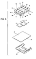
- Fig. 2 is an exploded perspective view of the module and a connector illustrated in Fig. 1.
- the antenna-integrated module illustrated in the above drawings mainly includes a rectangular circuit board 1, a group of circuit components 3, and a cover and antenna element 4.
- the circuit board 1 has an upper surface provided with a wiring pattern (not illustrated) of a high frequency circuit, and a lower surface, nearly the entirety of which is provided with an earth conductor layer 2.
- the group of circuit components 3 includes chip components, integrated circuits, and the like mounted on the upper surface of the circuit board 1 and connected to the wiring pattern.
- the cover and antenna element 4 is formed by a metal plate and mounted on the circuit board 1 to cover the group of circuit components 3.
- the circuit board 1 is electrically and mechanically connected onto a not-illustrated mother board via a connector 20.
- the cover and antenna element 4 includes a top board 5, a feed leg piece 6, short leg pieces 7 and 8, holding leg pieces 9 to 11, and side plates 12 to 15.
- the top board 5 is a flat rectangular metal plate for covering the group of circuit components 3, and operates as a radiating conductor.
- the feed leg piece 6, the short leg pieces 7 and 8, and the holding leg pieces 9 to 11 hang toward the circuit board 1 from the periphery of the top board 5.
- the side plates 12 to 15 hang toward the circuit board 1 from other positions than the positions of the above respective leg pieces 6 to 11 on the periphery (i.e., the four sides) of the top board 5.
- the feed leg piece 6 is connected to the wiring pattern, and the short leg pieces 7 and 8 are connected to the earth conductor layer 2.
- the holding leg pieces 9 to 11 are fixed to the circuit board 1 in an electrically open state.
- the top board 5 is pierced with slit-shaped openings 5a at six positions apart from the periphery thereof, and the respective side plates 12 to 15 are pierced with slit-shaped openings 12a to 15a, with each of the side plates having the corresponding openings at two positions apart from the periphery thereof.
- the side plate 12 extending along one of the long sides of the top board 5 is a bent piece, one side of which in the longer direction of the top board 5 continues to the feed leg piece 6, and the other side of which in the longer direction of the top board 5 continues to the holding leg piece 11.
- the side plate 12 is pierced with the openings 12a, which extend along the long side of the top board 5, at two positions in a line.
- the short leg piece 7 is provided at a position adjacent to the side plate 12 with the interposition of the feed leg piece 6 and a cutout portion 16.
- the side plate 13 extending along the other long side of the top board 5 is a bent piece, one side of which in the longer direction of the top board 5 continues to the short leg piece 8, and the other side of which in the longer direction of the top board 5 continues to the holding leg piece 9.
- the side plate 13 is pierced with the openings 13a, which extend along the long side of the top board 5, at two positions in a line.
- the holding leg piece 10 is provided at a position adjacent to the side plate 13 with the interposition of the holding leg piece 9 and a cutout portion 17.
- the side plate 14 extending over the entire length of one of the short sides of the top board 5 is pierced with the openings 14a, which extend along the short side, at two positions in a line.
- each of the slit-shaped openings 12a to 15a pierced in the respective side plates 12 to 15 is set to be equal to or less than 1 millimeter.
- each of the leading ends (i.e., the lower ends) of the respective side plates 12 to 15 faces the circuit board 1 with a clearance therebetween, and the opposed interval therebetween is also set to be equal to or less than 1 millimeter.
- a lower portion of the feed leg piece 6 is connected to a feed line of the above-described wiring pattern so that a predetermined high frequency signal is supplied to a feeding point of the top board 5 (i.e., an upper bent end portion of the feed leg piece 6) via the feed leg piece 6.
- the short leg pieces 7 and 8 are connected to the earth conductor layer 2 through holes formed in the circuit board 1.
- the holding leg pieces 9 to 11 are respectively connected to electrically isolated solder lands on the circuit board 1 so that an electrostatic capacitance is loaded between each of the solder lands and the earth conductor layer 2.
- the cover and antenna element 4 is attached onto the circuit board 1 in a stable posture, and the top board 5 faces the circuit board 1 with a predetermined interval therebetween. Further, as illustrated in the drawings, the four corners of the cover and antenna element 4 are provided with the short leg pieces 7 and 8 and the holding leg pieces 10 and 11, and the holding leg piece 9 having the same shape as the shape of the feed leg piece 6 is provided at a position point-symmetrical to the feed leg piece 6. Accordingly, the cover and antenna element 4 is designed to have an exterior of a symmetrical shape that does not change even if the opposite sides in the longer direction of the cover and antenna element 4 are reversed in direction.
- the cover and antenna element 4 formed by a metal plate for covering the group of circuit components 3 is connected to the earth conductor layer 2.
- the cover and antenna element 4 can be operated as a shield case.
- the rectangular top board 5 of the cover and antenna element 4 is provided with the short leg pieces 7 and 8 on one side in the longer direction thereof, and is kept in an electrically open state on the other side in the longer direction thereof.
- the top board 5 can be excited by power feeding from the feed leg piece 6. Accordingly, the top board 5 can be operated as a radiating conductor of an inverted-F antenna formed by a metal plate.
- the cover and antenna element 4 for covering the major portion of the high frequency circuit is designed to operate not only as the shield case but also as the antenna element of the inverted-F antenna.
- the present antenna-integrated module is more easily reduced in size and cost than the module configured such that the separate components of the antenna element and the shield case are planarly juxtaposed.
- the cover and antenna element 4 is designed to load the electrostatic capacitance on the electrically open side on which the holding leg pieces 9 to 11 concentrate, i.e., the side on which an electric field is formed at the time of power feeding. Accordingly, the size reduction of the entire module is further easily facilitated.
- the present antenna-integrated module a plurality of the openings 5a and 12a to 15a are respectively pierced in the top board 5 and the respective side plates 12 to 15 of the cover and antenna element 4, and thus air can be smoothly flowed through the openings 5a and 12a to 15a.
- the heat is easily transmitted to the region on the circuit board 1 covered by the cover and antenna element 4, and thus reflow soldering can be performed at one time on the cover and antenna element 4 and on the group of circuit components 3 mounted on the circuit board 1. That is, there is no need to repeat the reflow process. Accordingly, the module can be further inexpensively manufactured.
- the side plates 12 to 15 hang toward the circuit board 1 from the periphery of the top board 5, and the opposed interval between the leading end of each of the side plates 12 to 15 and the circuit board 1 is set to be equal to or less than 1 millimeter. It is therefore difficult to insert a solder trowel or the like from a lateral side into the space covered by the cover and antenna element 4. Further, each of the openings 5a and 12a to 15a is formed into a slit shape having a width of equal to or less than 1 millimeter. Thus, it is also difficult to insert the solder trowel or the like into the openings 5a and 12a to 15a. According to the present antenna-integrated module, therefore, there is little risk that the major portion of the high frequency circuit is illegally altered.
- the cover and antenna element 4 formed by a metal plate is simple in shape and thus easy to be manufactured. Further, the cover and antenna element 4 is designed to have an exterior of a symmetrical shape that does not change even if the opposite sides in the longer direction of the cover and antenna element 4 are reversed in direction. Accordingly, the antenna-integrated module according to the present embodiment has an advantage in that there is no need to take trouble to check the direction of the cover and antenna element 4 in the assembly process of mounting the cover and antenna element 4 on the circuit board 1, and thus that the workability is improved.
- Fig. 3 is a perspective view of an antenna-integrated module according to a second embodiment of the present invention.
- Components corresponding to the components illustrated in Figs. 1 and 2 are assigned with the same reference numerals so that redundant description thereof will be omitted.
- the present embodiment is different from the above-described first embodiment in the positions formed with the feed leg piece 6, the short leg pieces 7 and 8, and the holding leg pieces 9 to 11, which hang from the periphery of the top board 5, and is basically similar to the first embodiment in the other configurations, operations, and effects. That is, the side plate 14 extending along one of the short sides of the top board 5 is a bent piece, one side of which in the shorter direction of the top board 5 continues to the feed leg piece 6, and a central portion and the other side of which in the shorter direction of the top board 5 continue to the short leg pieces 7 and 8.
- the side plate 15 extending along the other short side of the top board 5 is a bent piece, a central portion and the opposite sides of which in the shorter direction of the top board 5 continue to the holding leg pieces 9, 10, and 11.
- the side plate 12 extending over the entire length of one of the long sides of the top board 5 is pierced with the openings 12a, which extend along the long side, at two positions in a line.
- the side plate 13 extending over the entire length of the other long side of the top board 5 is pierced with the openings 13a, which extend along the long side, at two positions in a line.
- the respective openings 5a of the top board 5 extend along the longer direction of the top board 5.
- the respective openings 5a may extend along the shorter direction of the top board 5.
- each of the openings 5a and the openings 12a to 15a may be shaped into a small hole instead of a slit. In such a case, if a multitude of small holes are pierced, repetition of the reflow process can be prevented.
Landscapes
- Engineering & Computer Science (AREA)
- Computer Networks & Wireless Communication (AREA)
- Physics & Mathematics (AREA)
- Electromagnetism (AREA)
- Shielding Devices Or Components To Electric Or Magnetic Fields (AREA)
Abstract
Description
- The present invention relates to an antenna-integrated module suitable as a small-sized transmitting and receiving unit or the like used in communication and broadcasting.
- In recent years, along with the development of the wireless communication technique, there have been proposed a variety of electronic devices and wireless cards including therein a small-sized transmitting and receiving unit. A transmitting and receiving unit of this type is an antenna-integrated high frequency module including an antenna element on a circuit board provided with a high frequency circuit. A conventional general antenna-integrated module is configured such that a shield case formed by a metal plate covers a predetermined region on a circuit board provided with a major portion of a high frequency circuit, and that an antenna element such as a chip antenna and a pattern antenna is provided in another region on the circuit board (see
Pages 4 to 6 and Fig. 1 ofJapanese Unexamined Patent Application Publication No. 2002-232221 - In such a configuration that the antenna element and the shield case are juxtaposed in different regions on the circuit board, however, the entire module is increased in planar size. Thus, it is difficult to facilitate size reduction of the module. Further, if such a configuration is adopted that a chip antenna is used as the antenna element to be connected to the high frequency circuit via a coaxial cable, component cost is significantly increased.
- In recent years, therefore, there has been proposed an antenna-integrated module configured such that the shield case for covering and electromagnetically shielding a group of circuit components of the high frequency circuit can be used also as the antenna element of an inverted-F antenna (see
Pages Japanese Unexamined Patent Application Publication No. 2005-5866 - As described above, in the antenna-integrated module of the conventional proposal disclosed in
Japanese Unexamined Patent Application Publication No. 2005-5866 - Further, in the cover and antenna element used in the antenna-integrated module of the above conventional proposal, the plurality of bent leg pieces simply hang from the periphery of the top board. Thus, the space covered by the top board (i.e., the region mounted with the group of circuit components) is widely exposed, as viewed from a lateral side. Therefore, there is a possibility that a solder trowel or the like is inserted into the space from the lateral side for illegal alteration of the major portion of the high frequency circuit.
- The present invention has been made in view of the above-described circumferences of the conventional techniques, and an object of the present invention is to provide an antenna-integrated module which enables easy size reduction thereof, easy prevention of illegal alteration of a circuit thereof, effective performance of a reflow process thereon, and inexpensive manufacture thereof.
- To achieve the above-described object, an antenna-integrated module according to the present invention includes a circuit board provided with a wiring pattern and an earth conductor layer of a high frequency circuit, a group of circuit components mounted on a surface of the circuit board, and a cover and antenna element formed by a metal plate and mounted on the circuit board to cover the group of circuit components. The cover and antenna element includes a top board facing the circuit board with a predetermined interval therebetween and operating as a radiating conductor, a feed leg piece hanging toward the circuit board from a feeding point of the top board and connected to the wiring pattern, short leg pieces hanging toward the circuit board from the periphery of one side of the top board and connected to the earth conductor layer, electrically open holding leg pieces hanging toward the circuit board from the periphery of the other side of the top board and fixed to the circuit board, and side plates hanging toward the circuit board from other positions than the positions of the feed leg piece, the short leg pieces, and the holding leg pieces on the periphery of the top board such that the leading ends of the side plates face the circuit board with a clearance therebetween. The top board is pierced with openings in the form of slits or small holes at a plurality of positions apart from the periphery thereof.
- In the thus configured antenna-integrated module according to the present invention, the cover and antenna element formed by a metal plate can be operated as a shield case for electromagnetically shielding the group of circuit components of the high frequency circuit, and also as an antenna element of an inverted-F antenna formed by a metal plate, in which the top board acts as a radiating conductor. Therefore, the entirety of the module is more easily reduced in size and cost than the module configured such that separate components of an antenna element and a shield case are planarly juxtaposed. Further, the top board is pierced with the openings at a plurality of positions, and thus air can be smoothly flowed through the openings. In a reflow process, therefore, the heat is easily transmitted to the region on the circuit board covered by the cover and antenna element. Thus, reflow soldering can be performed at one time on the cover and antenna element and on the group of circuit components mounted on the circuit board. Therefore, manufacturing cost can be further reduced. Furthermore, since the openings are formed into slits or small holes, it is difficult to insert a solder trowel or the like into the openings. Further, since the side plates hang toward the circuit board from the periphery of the top board, it is also difficult to insert the solder trowel or the like from a lateral side into the space covered by the cover and antenna element. Accordingly, the present antenna-integrated module has little risk of illegal alteration of a major portion of the high frequency circuit.
- In the above-described configuration, the openings in the form of slits or small holes may be also pierced in each of the side plates of the cover and antenna element at a plurality of positions apart from the periphery of the side plate. This configuration is preferable in that the heat is further easily transmitted to the region on the circuit board covered by the cover and antenna element in the reflow process.
- Further, in the above-described configuration, the top board of the cover and antenna element may be rectangular, and the respective short leg pieces may hang from two positions on one side in the longer direction of the top board, while the respective holding leg pieces may hang from two positions on the other side in the longer direction of the top board. This configuration is preferable in that the cover and antenna element can be simplified in shape and thus easily manufactured. In this case, the third holding leg piece having the same shape as the shape of the feed leg piece may be provided at a position point-symmetrical to the feed leg piece such that the cover and antenna element has an exterior of a symmetrical shape that does not change even if the opposite sides in the longer direction of the cover and antenna element are reversed in direction. Thus configured, there is no need to check the direction of the cover and antenna element in the assembly process of mounting the cover and antenna element on the circuit board. Accordingly, the workability can be improved.
- Furthermore, in the above-described configuration, the width of the openings pierced in the top board and the side plates and the opposed interval (i.e., the size of the clearance) between the leading ends of the side plates and the circuit board may be both set to be equal to or less than 1 millimeter. This configuration is preferable in that the illegal alteration of the major portion of the high frequency circuit can be further reliably prevented.
-
- Fig. 1 is a perspective view of an antenna-integrated module according to a first embodiment of the present invention;
- Fig. 2 is an exploded perspective view of the module and a connector illustrated in Fig. 1; and
- Fig. 3 is a perspective view of an antenna-integrated module according to a second embodiment of the present invention.
- Embodiments of the present invention will now be described with reference to the drawings. Fig. 1 is a perspective view of an antenna-integrated module according to a first embodiment of the present invention, and Fig. 2 is an exploded perspective view of the module and a connector illustrated in Fig. 1.
- The antenna-integrated module illustrated in the above drawings mainly includes a
rectangular circuit board 1, a group ofcircuit components 3, and a cover andantenna element 4. Thecircuit board 1 has an upper surface provided with a wiring pattern (not illustrated) of a high frequency circuit, and a lower surface, nearly the entirety of which is provided with anearth conductor layer 2. The group ofcircuit components 3 includes chip components, integrated circuits, and the like mounted on the upper surface of thecircuit board 1 and connected to the wiring pattern. The cover andantenna element 4 is formed by a metal plate and mounted on thecircuit board 1 to cover the group ofcircuit components 3. Thecircuit board 1 is electrically and mechanically connected onto a not-illustrated mother board via aconnector 20. - The cover and
antenna element 4 includes atop board 5, afeed leg piece 6,short leg pieces leg pieces 9 to 11, andside plates 12 to 15. Thetop board 5 is a flat rectangular metal plate for covering the group ofcircuit components 3, and operates as a radiating conductor. Thefeed leg piece 6, theshort leg pieces holding leg pieces 9 to 11 hang toward thecircuit board 1 from the periphery of thetop board 5. Theside plates 12 to 15 hang toward thecircuit board 1 from other positions than the positions of the aboverespective leg pieces 6 to 11 on the periphery (i.e., the four sides) of thetop board 5. Thefeed leg piece 6 is connected to the wiring pattern, and theshort leg pieces earth conductor layer 2. Meanwhile, the holdingleg pieces 9 to 11 are fixed to thecircuit board 1 in an electrically open state. Further, thetop board 5 is pierced with slit-shapedopenings 5a at six positions apart from the periphery thereof, and therespective side plates 12 to 15 are pierced with slit-shapedopenings 12a to 15a, with each of the side plates having the corresponding openings at two positions apart from the periphery thereof. - That is, the
side plate 12 extending along one of the long sides of thetop board 5 is a bent piece, one side of which in the longer direction of thetop board 5 continues to thefeed leg piece 6, and the other side of which in the longer direction of thetop board 5 continues to the holdingleg piece 11. Theside plate 12 is pierced with theopenings 12a, which extend along the long side of thetop board 5, at two positions in a line. Further, theshort leg piece 7 is provided at a position adjacent to theside plate 12 with the interposition of thefeed leg piece 6 and acutout portion 16. Similarly, theside plate 13 extending along the other long side of thetop board 5 is a bent piece, one side of which in the longer direction of thetop board 5 continues to theshort leg piece 8, and the other side of which in the longer direction of thetop board 5 continues to the holdingleg piece 9. Theside plate 13 is pierced with theopenings 13a, which extend along the long side of thetop board 5, at two positions in a line. Further, the holdingleg piece 10 is provided at a position adjacent to theside plate 13 with the interposition of the holdingleg piece 9 and acutout portion 17. Furthermore, theside plate 14 extending over the entire length of one of the short sides of thetop board 5 is pierced with theopenings 14a, which extend along the short side, at two positions in a line. Similarly, theside plate 15 extending over the entire length of the other short side of thetop board 5 is pierced with theopenings 15a, which extend along the short side, at two positions in a line. The width (i.e., the slit width) of each of the slit-shapedopenings 12a to 15a pierced in therespective side plates 12 to 15 is set to be equal to or less than 1 millimeter. Further, each of the leading ends (i.e., the lower ends) of therespective side plates 12 to 15 faces thecircuit board 1 with a clearance therebetween, and the opposed interval therebetween is also set to be equal to or less than 1 millimeter. - The
respective leg pieces 6 to 11 of the cover andantenna element 4 will now be described in detail. A lower portion of thefeed leg piece 6 is connected to a feed line of the above-described wiring pattern so that a predetermined high frequency signal is supplied to a feeding point of the top board 5 (i.e., an upper bent end portion of the feed leg piece 6) via thefeed leg piece 6. Theshort leg pieces earth conductor layer 2 through holes formed in thecircuit board 1. The holdingleg pieces 9 to 11 are respectively connected to electrically isolated solder lands on thecircuit board 1 so that an electrostatic capacitance is loaded between each of the solder lands and theearth conductor layer 2. That is, with therespective leg pieces 6 to 11 solder-joined to the corresponding solder lands, the cover andantenna element 4 is attached onto thecircuit board 1 in a stable posture, and thetop board 5 faces thecircuit board 1 with a predetermined interval therebetween. Further, as illustrated in the drawings, the four corners of the cover andantenna element 4 are provided with theshort leg pieces leg pieces leg piece 9 having the same shape as the shape of thefeed leg piece 6 is provided at a position point-symmetrical to thefeed leg piece 6. Accordingly, the cover andantenna element 4 is designed to have an exterior of a symmetrical shape that does not change even if the opposite sides in the longer direction of the cover andantenna element 4 are reversed in direction. - In the thus configured antenna-integrated module, the cover and
antenna element 4 formed by a metal plate for covering the group ofcircuit components 3 is connected to theearth conductor layer 2. Thus, the cover andantenna element 4 can be operated as a shield case. Further, the rectangulartop board 5 of the cover andantenna element 4 is provided with theshort leg pieces top board 5 can be excited by power feeding from thefeed leg piece 6. Accordingly, thetop board 5 can be operated as a radiating conductor of an inverted-F antenna formed by a metal plate. - That is, in the antenna-integrated module according to the present embodiment, the cover and
antenna element 4 for covering the major portion of the high frequency circuit is designed to operate not only as the shield case but also as the antenna element of the inverted-F antenna. Thus, the present antenna-integrated module is more easily reduced in size and cost than the module configured such that the separate components of the antenna element and the shield case are planarly juxtaposed. Further, the cover andantenna element 4 is designed to load the electrostatic capacitance on the electrically open side on which the holdingleg pieces 9 to 11 concentrate, i.e., the side on which an electric field is formed at the time of power feeding. Accordingly, the size reduction of the entire module is further easily facilitated. - Furthermore, in the present antenna-integrated module, a plurality of the
openings top board 5 and therespective side plates 12 to 15 of the cover andantenna element 4, and thus air can be smoothly flowed through theopenings circuit board 1 covered by the cover andantenna element 4, and thus reflow soldering can be performed at one time on the cover andantenna element 4 and on the group ofcircuit components 3 mounted on thecircuit board 1. That is, there is no need to repeat the reflow process. Accordingly, the module can be further inexpensively manufactured. - In addition, in the present antenna-integrated module, the
side plates 12 to 15 hang toward thecircuit board 1 from the periphery of thetop board 5, and the opposed interval between the leading end of each of theside plates 12 to 15 and thecircuit board 1 is set to be equal to or less than 1 millimeter. It is therefore difficult to insert a solder trowel or the like from a lateral side into the space covered by the cover andantenna element 4. Further, each of theopenings openings - Furthermore, in the antenna-integrated module according to the present embodiment, the cover and
antenna element 4 formed by a metal plate is simple in shape and thus easy to be manufactured. Further, the cover andantenna element 4 is designed to have an exterior of a symmetrical shape that does not change even if the opposite sides in the longer direction of the cover andantenna element 4 are reversed in direction. Accordingly, the antenna-integrated module according to the present embodiment has an advantage in that there is no need to take trouble to check the direction of the cover andantenna element 4 in the assembly process of mounting the cover andantenna element 4 on thecircuit board 1, and thus that the workability is improved. - Fig. 3 is a perspective view of an antenna-integrated module according to a second embodiment of the present invention. Components corresponding to the components illustrated in Figs. 1 and 2 are assigned with the same reference numerals so that redundant description thereof will be omitted.
- The present embodiment is different from the above-described first embodiment in the positions formed with the
feed leg piece 6, theshort leg pieces leg pieces 9 to 11, which hang from the periphery of thetop board 5, and is basically similar to the first embodiment in the other configurations, operations, and effects. That is, theside plate 14 extending along one of the short sides of thetop board 5 is a bent piece, one side of which in the shorter direction of thetop board 5 continues to thefeed leg piece 6, and a central portion and the other side of which in the shorter direction of thetop board 5 continue to theshort leg pieces side plate 15 extending along the other short side of thetop board 5 is a bent piece, a central portion and the opposite sides of which in the shorter direction of thetop board 5 continue to the holdingleg pieces side plate 12 extending over the entire length of one of the long sides of thetop board 5 is pierced with theopenings 12a, which extend along the long side, at two positions in a line. Similarly, theside plate 13 extending over the entire length of the other long side of thetop board 5 is pierced with theopenings 13a, which extend along the long side, at two positions in a line. - In the respective embodiments as described above, the
respective openings 5a of thetop board 5 extend along the longer direction of thetop board 5. However, therespective openings 5a may extend along the shorter direction of thetop board 5. Further, each of theopenings 5a and theopenings 12a to 15a may be shaped into a small hole instead of a slit. In such a case, if a multitude of small holes are pierced, repetition of the reflow process can be prevented.
Claims (5)
- An antenna-integrated module comprising:a circuit board provided with a wiring pattern and an earth conductor layer of a high frequency circuit;a group of circuit components mounted on a surface of the circuit board; anda cover and antenna element formed by a metal plate and mounted on the circuit board to cover the group of circuit components,wherein the cover and antenna element includesa top board facing the circuit board with a predetermined interval therebetween, and operating as a radiating conductor,a feed leg piece hanging toward the circuit board from a feeding point of the top board, and connected to the wiring pattern,short leg pieces hanging toward the circuit board from the periphery of one side of the top board, and connected to the earth conductor layer,electrically open holding leg pieces hanging toward the circuit board from the periphery of the other side of the top board, and fixed to the circuit board, andside plates hanging toward the circuit board from other positions than the positions of the feed leg piece, the short leg pieces, and the holding leg pieces on the periphery of the top board such that the leading ends of the side plates face the circuit board with a clearance therebetween, andwherein the top board is pierced with openings in the form of slits or small holes at a plurality of positions apart from the periphery thereof.
- The antenna-integrated module according to Claim 1,
wherein the openings in the form of slits or small holes are also pierced in each of the side plates at a plurality of positions apart from the periphery of the side plate. - The antenna-integrated module according to either one of Claims 1 and 2,
wherein the top board is rectangular, and
wherein the respective short leg pieces hang from two positions on one side in the longer direction of the top board, and the respective holding leg pieces hang from two positions on the other side in the longer direction of the top board. - The antenna-integrated module according to Claim 3,
wherein a third holding leg piece having the same shape as the shape of the feed leg piece is provided at a position point-symmetrical to the feed leg piece such that the cover and antenna element has an exterior of a symmetrical shape that does not change even if the opposite sides in the longer direction of the cover and antenna element are reversed in direction. - The antenna-integrated module according to any one of Claims 1 to 4,
wherein the width of the openings and the opposed interval between the leading ends of the side plates and the circuit board are both set to be equal to or less than 1 millimeter.
Applications Claiming Priority (1)
| Application Number | Priority Date | Filing Date | Title |
|---|---|---|---|
| JP2006045828 | 2006-02-22 |
Publications (1)
| Publication Number | Publication Date |
|---|---|
| EP1826867A1 true EP1826867A1 (en) | 2007-08-29 |
Family
ID=38024395
Family Applications (1)
| Application Number | Title | Priority Date | Filing Date |
|---|---|---|---|
| EP07003436A Withdrawn EP1826867A1 (en) | 2006-02-22 | 2007-02-19 | Antenna-integrated module |
Country Status (1)
| Country | Link |
|---|---|
| EP (1) | EP1826867A1 (en) |
Cited By (5)
| Publication number | Priority date | Publication date | Assignee | Title |
|---|---|---|---|---|
| EP1933416A1 (en) * | 2006-12-13 | 2008-06-18 | Alps Electric Co., Ltd. | Antenna-integrated module |
| EP2387100A1 (en) * | 2010-04-29 | 2011-11-16 | Laird Technologies AB | A metal cover for a radio communication device |
| EP3474377A1 (en) * | 2017-10-19 | 2019-04-24 | Raspberry PI (Trading) Limited | Radio module |
| CN114938682A (en) * | 2020-01-10 | 2022-08-23 | 株式会社村田制作所 | Module |
| US20240356212A1 (en) * | 2021-08-27 | 2024-10-24 | Amotech Co., Ltd. | Shield can having antenna function and electronic module comprising same |
Citations (8)
| Publication number | Priority date | Publication date | Assignee | Title |
|---|---|---|---|---|
| JPH0575286A (en) * | 1991-09-13 | 1993-03-26 | Matsushita Electric Ind Co Ltd | Method of manufacturing printed circuit |
| EP0621653A2 (en) * | 1993-04-23 | 1994-10-26 | Murata Manufacturing Co., Ltd. | Surface-mountable antenna unit |
| JPH07170087A (en) * | 1993-12-16 | 1995-07-04 | Matsushita Electric Ind Co Ltd | Shield configuration method |
| US5442521A (en) * | 1991-09-19 | 1995-08-15 | Nokia Mobile Phones Ltd. | Circuit board assembly |
| EP1137099A2 (en) * | 2000-03-16 | 2001-09-26 | Nokia Mobile Phones Ltd. | Antenna connector |
| JP2003188620A (en) * | 2001-12-19 | 2003-07-04 | Murata Mfg Co Ltd | Module integrated antenna |
| JP2004312044A (en) * | 2004-07-21 | 2004-11-04 | Ngk Spark Plug Co Ltd | Wiring board with shield cap and method of manufacturing the same |
| US20050104785A1 (en) * | 2003-11-18 | 2005-05-19 | Dell Products L.P. | Information handling system including passive RF tuning carrier for wireless modules |
-
2007
- 2007-02-19 EP EP07003436A patent/EP1826867A1/en not_active Withdrawn
Patent Citations (8)
| Publication number | Priority date | Publication date | Assignee | Title |
|---|---|---|---|---|
| JPH0575286A (en) * | 1991-09-13 | 1993-03-26 | Matsushita Electric Ind Co Ltd | Method of manufacturing printed circuit |
| US5442521A (en) * | 1991-09-19 | 1995-08-15 | Nokia Mobile Phones Ltd. | Circuit board assembly |
| EP0621653A2 (en) * | 1993-04-23 | 1994-10-26 | Murata Manufacturing Co., Ltd. | Surface-mountable antenna unit |
| JPH07170087A (en) * | 1993-12-16 | 1995-07-04 | Matsushita Electric Ind Co Ltd | Shield configuration method |
| EP1137099A2 (en) * | 2000-03-16 | 2001-09-26 | Nokia Mobile Phones Ltd. | Antenna connector |
| JP2003188620A (en) * | 2001-12-19 | 2003-07-04 | Murata Mfg Co Ltd | Module integrated antenna |
| US20050104785A1 (en) * | 2003-11-18 | 2005-05-19 | Dell Products L.P. | Information handling system including passive RF tuning carrier for wireless modules |
| JP2004312044A (en) * | 2004-07-21 | 2004-11-04 | Ngk Spark Plug Co Ltd | Wiring board with shield cap and method of manufacturing the same |
Cited By (7)
| Publication number | Priority date | Publication date | Assignee | Title |
|---|---|---|---|---|
| EP1933416A1 (en) * | 2006-12-13 | 2008-06-18 | Alps Electric Co., Ltd. | Antenna-integrated module |
| EP2387100A1 (en) * | 2010-04-29 | 2011-11-16 | Laird Technologies AB | A metal cover for a radio communication device |
| EP3474377A1 (en) * | 2017-10-19 | 2019-04-24 | Raspberry PI (Trading) Limited | Radio module |
| GB2567812A (en) * | 2017-10-19 | 2019-05-01 | Raspberry Pi Trading Ltd | Radio module |
| CN114938682A (en) * | 2020-01-10 | 2022-08-23 | 株式会社村田制作所 | Module |
| US20240356212A1 (en) * | 2021-08-27 | 2024-10-24 | Amotech Co., Ltd. | Shield can having antenna function and electronic module comprising same |
| US12592483B2 (en) * | 2021-08-27 | 2026-03-31 | Amotech Co., Ltd. | Shield can having antenna function and electronic module comprising same |
Similar Documents
| Publication | Publication Date | Title |
|---|---|---|
| EP1933416A1 (en) | Antenna-integrated module | |
| US6958732B2 (en) | Small-sized and high-gained antenna-integrated module | |
| US7123197B2 (en) | Miniaturized antenna-coupled module | |
| US6879849B2 (en) | In-built antenna for mobile communication device | |
| JP4160944B2 (en) | Antenna device | |
| US11640860B2 (en) | Circuit module and interposer | |
| JP3134262U (en) | Surface mount connector | |
| JP2022159893A (en) | Communication device | |
| US7309240B2 (en) | Apparatus and electronic apparatus | |
| WO2010073418A1 (en) | Portable wireless apparatus | |
| JP2004319381A (en) | Grounding terminal | |
| JP2008072559A (en) | Antenna system and manufacturing method thereof | |
| JP2002353726A (en) | Small antenna | |
| US20090303151A1 (en) | Low profile gps antenna assembly | |
| JP2024166943A (en) | Antenna device and antenna board | |
| JP2007259412A (en) | Antenna-integrated module | |
| JP2004319384A (en) | Electronic circuit unit | |
| JP2005354368A (en) | Waveguide directional coupler | |
| JP2007159064A (en) | ANTENNA AND RADIO DEVICE AND ELECTRONIC DEVICE USING THE SAME | |
| JP2001223604A (en) | Wireless communication module | |
| JPH04322498A (en) | High-frequency apparatus | |
| JP2007281581A (en) | Diversity antenna device | |
| JP2003234548A (en) | Printed wiring board | |
| JP4160948B2 (en) | Antenna device | |
| JP4146002B2 (en) | Electronic component mounting module |
Legal Events
| Date | Code | Title | Description |
|---|---|---|---|
| PUAI | Public reference made under article 153(3) epc to a published international application that has entered the european phase |
Free format text: ORIGINAL CODE: 0009012 |
|
| AK | Designated contracting states |
Kind code of ref document: A1 Designated state(s): AT BE BG CH CY CZ DE DK EE ES FI FR GB GR HU IE IS IT LI LT LU LV MC NL PL PT RO SE SI SK TR |
|
| AX | Request for extension of the european patent |
Extension state: AL BA HR MK YU |
|
| 17P | Request for examination filed |
Effective date: 20070726 |
|
| AKX | Designation fees paid |
Designated state(s): DE FR GB |
|
| 17Q | First examination report despatched |
Effective date: 20080425 |
|
| STAA | Information on the status of an ep patent application or granted ep patent |
Free format text: STATUS: THE APPLICATION HAS BEEN WITHDRAWN |
|
| 18W | Application withdrawn |
Effective date: 20090820 |