EP1826746A2 - Liquid crystal display device - Google Patents
Liquid crystal display device Download PDFInfo
- Publication number
- EP1826746A2 EP1826746A2 EP07002020A EP07002020A EP1826746A2 EP 1826746 A2 EP1826746 A2 EP 1826746A2 EP 07002020 A EP07002020 A EP 07002020A EP 07002020 A EP07002020 A EP 07002020A EP 1826746 A2 EP1826746 A2 EP 1826746A2
- Authority
- EP
- European Patent Office
- Prior art keywords
- low
- pixel
- data
- image signal
- rgb
- Prior art date
- Legal status (The legal status is an assumption and is not a legal conclusion. Google has not performed a legal analysis and makes no representation as to the accuracy of the status listed.)
- Granted
Links
Images




Classifications
-
- G—PHYSICS
- G09—EDUCATION; CRYPTOGRAPHY; DISPLAY; ADVERTISING; SEALS
- G09G—ARRANGEMENTS OR CIRCUITS FOR CONTROL OF INDICATING DEVICES USING STATIC MEANS TO PRESENT VARIABLE INFORMATION
- G09G3/00—Control arrangements or circuits, of interest only in connection with visual indicators other than cathode-ray tubes
- G09G3/20—Control arrangements or circuits, of interest only in connection with visual indicators other than cathode-ray tubes for presentation of an assembly of a number of characters, e.g. a page, by composing the assembly by combination of individual elements arranged in a matrix no fixed position being assigned to or needed to be assigned to the individual characters or partial characters
- G09G3/34—Control arrangements or circuits, of interest only in connection with visual indicators other than cathode-ray tubes for presentation of an assembly of a number of characters, e.g. a page, by composing the assembly by combination of individual elements arranged in a matrix no fixed position being assigned to or needed to be assigned to the individual characters or partial characters by control of light from an independent source
- G09G3/36—Control arrangements or circuits, of interest only in connection with visual indicators other than cathode-ray tubes for presentation of an assembly of a number of characters, e.g. a page, by composing the assembly by combination of individual elements arranged in a matrix no fixed position being assigned to or needed to be assigned to the individual characters or partial characters by control of light from an independent source using liquid crystals
- G09G3/3611—Control of matrices with row and column drivers
- G09G3/3648—Control of matrices with row and column drivers using an active matrix
-
- B—PERFORMING OPERATIONS; TRANSPORTING
- B60—VEHICLES IN GENERAL
- B60N—SEATS SPECIALLY ADAPTED FOR VEHICLES; VEHICLE PASSENGER ACCOMMODATION NOT OTHERWISE PROVIDED FOR
- B60N2/00—Seats specially adapted for vehicles; Arrangement or mounting of seats in vehicles
- B60N2/005—Arrangement or mounting of seats in vehicles, e.g. dismountable auxiliary seats
- B60N2/01—Arrangement of seats relative to one another
- B60N2/012—The seat support being a part of the vehicle body or chassis
-
- B—PERFORMING OPERATIONS; TRANSPORTING
- B60—VEHICLES IN GENERAL
- B60N—SEATS SPECIALLY ADAPTED FOR VEHICLES; VEHICLE PASSENGER ACCOMMODATION NOT OTHERWISE PROVIDED FOR
- B60N2/00—Seats specially adapted for vehicles; Arrangement or mounting of seats in vehicles
- B60N2/24—Seats specially adapted for vehicles; Arrangement or mounting of seats in vehicles for particular purposes or particular vehicles
- B60N2/242—Bus seats
-
- G—PHYSICS
- G09—EDUCATION; CRYPTOGRAPHY; DISPLAY; ADVERTISING; SEALS
- G09G—ARRANGEMENTS OR CIRCUITS FOR CONTROL OF INDICATING DEVICES USING STATIC MEANS TO PRESENT VARIABLE INFORMATION
- G09G3/00—Control arrangements or circuits, of interest only in connection with visual indicators other than cathode-ray tubes
- G09G3/20—Control arrangements or circuits, of interest only in connection with visual indicators other than cathode-ray tubes for presentation of an assembly of a number of characters, e.g. a page, by composing the assembly by combination of individual elements arranged in a matrix no fixed position being assigned to or needed to be assigned to the individual characters or partial characters
- G09G3/34—Control arrangements or circuits, of interest only in connection with visual indicators other than cathode-ray tubes for presentation of an assembly of a number of characters, e.g. a page, by composing the assembly by combination of individual elements arranged in a matrix no fixed position being assigned to or needed to be assigned to the individual characters or partial characters by control of light from an independent source
- G09G3/36—Control arrangements or circuits, of interest only in connection with visual indicators other than cathode-ray tubes for presentation of an assembly of a number of characters, e.g. a page, by composing the assembly by combination of individual elements arranged in a matrix no fixed position being assigned to or needed to be assigned to the individual characters or partial characters by control of light from an independent source using liquid crystals
- G09G3/3607—Control arrangements or circuits, of interest only in connection with visual indicators other than cathode-ray tubes for presentation of an assembly of a number of characters, e.g. a page, by composing the assembly by combination of individual elements arranged in a matrix no fixed position being assigned to or needed to be assigned to the individual characters or partial characters by control of light from an independent source using liquid crystals for displaying colours or for displaying grey scales with a specific pixel layout, e.g. using sub-pixels
-
- B—PERFORMING OPERATIONS; TRANSPORTING
- B60—VEHICLES IN GENERAL
- B60Y—INDEXING SCHEME RELATING TO ASPECTS CROSS-CUTTING VEHICLE TECHNOLOGY
- B60Y2200/00—Type of vehicle
- B60Y2200/10—Road Vehicles
- B60Y2200/14—Trucks; Load vehicles, Busses
- B60Y2200/143—Busses
-
- G—PHYSICS
- G09—EDUCATION; CRYPTOGRAPHY; DISPLAY; ADVERTISING; SEALS
- G09G—ARRANGEMENTS OR CIRCUITS FOR CONTROL OF INDICATING DEVICES USING STATIC MEANS TO PRESENT VARIABLE INFORMATION
- G09G2300/00—Aspects of the constitution of display devices
- G09G2300/04—Structural and physical details of display devices
- G09G2300/0439—Pixel structures
- G09G2300/0443—Pixel structures with several sub-pixels for the same colour in a pixel, not specifically used to display gradations
- G09G2300/0447—Pixel structures with several sub-pixels for the same colour in a pixel, not specifically used to display gradations for multi-domain technique to improve the viewing angle in a liquid crystal display, such as multi-vertical alignment [MVA]
-
- G—PHYSICS
- G09—EDUCATION; CRYPTOGRAPHY; DISPLAY; ADVERTISING; SEALS
- G09G—ARRANGEMENTS OR CIRCUITS FOR CONTROL OF INDICATING DEVICES USING STATIC MEANS TO PRESENT VARIABLE INFORMATION
- G09G2320/00—Control of display operating conditions
- G09G2320/02—Improving the quality of display appearance
- G09G2320/0271—Adjustment of the gradation levels within the range of the gradation scale, e.g. by redistribution or clipping
- G09G2320/0276—Adjustment of the gradation levels within the range of the gradation scale, e.g. by redistribution or clipping for the purpose of adaptation to the characteristics of a display device, i.e. gamma correction
-
- G—PHYSICS
- G09—EDUCATION; CRYPTOGRAPHY; DISPLAY; ADVERTISING; SEALS
- G09G—ARRANGEMENTS OR CIRCUITS FOR CONTROL OF INDICATING DEVICES USING STATIC MEANS TO PRESENT VARIABLE INFORMATION
- G09G2320/00—Control of display operating conditions
- G09G2320/02—Improving the quality of display appearance
- G09G2320/028—Improving the quality of display appearance by changing the viewing angle properties, e.g. widening the viewing angle, adapting the viewing angle to the view direction
-
- G—PHYSICS
- G09—EDUCATION; CRYPTOGRAPHY; DISPLAY; ADVERTISING; SEALS
- G09G—ARRANGEMENTS OR CIRCUITS FOR CONTROL OF INDICATING DEVICES USING STATIC MEANS TO PRESENT VARIABLE INFORMATION
- G09G2320/00—Control of display operating conditions
- G09G2320/06—Adjustment of display parameters
- G09G2320/0666—Adjustment of display parameters for control of colour parameters, e.g. colour temperature
-
- G—PHYSICS
- G09—EDUCATION; CRYPTOGRAPHY; DISPLAY; ADVERTISING; SEALS
- G09G—ARRANGEMENTS OR CIRCUITS FOR CONTROL OF INDICATING DEVICES USING STATIC MEANS TO PRESENT VARIABLE INFORMATION
- G09G5/00—Control arrangements or circuits for visual indicators common to cathode-ray tube indicators and other visual indicators
- G09G5/02—Control arrangements or circuits for visual indicators common to cathode-ray tube indicators and other visual indicators characterised by the way in which colour is displayed
- G09G5/06—Control arrangements or circuits for visual indicators common to cathode-ray tube indicators and other visual indicators characterised by the way in which colour is displayed using colour palettes, e.g. look-up tables
Definitions
- the present disclosure relates to a display device, and more particularly, to a display device having an improved side visibility.
- a liquid crystal display (“LCD”) apparatus can include two substrates and a liquid crystal layer interposed between the two substrates.
- the liquid crystal layer varies arrangement of liquid crystal molecules in response to an electric field applied thereto, thus light transmitted through the liquid crystal layer may be changed to display an image.
- the liquid crystal layer of the LCD device has anisotropy so that an image display quality of the LCD device varies based on a viewing angle.
- the LCD device may have a narrow range of a viewing angle than other display devices to show an image of good display quality. Therefore, in order to improve a wide viewing angle, a vertically aligned ("VA") mode LCD device has been developed.
- VA vertically aligned
- the VA mode LCD device includes a liquid crystal layer having a negative type anisotropic dielectric constant.
- the liquid crystal layer is sealed between two substrates.
- the two substrates are vertically aligned with each other.
- Liquid crystal molecules of the liquid crystal layer have hometropic characteristics.
- the liquid crystal molecules are substantially vertically arranged with respect to the two substrates such that a black image is displayed.
- the liquid crystal molecules When a relatively high electric field is applied to the two substrates, the liquid crystal molecules are substantially perpendicularly arranged with respect to the two substrates such that a white image is displayed. Furthermore, when an electric field that is less than the high electric field is applied to the two substrates, the liquid crystal molecules are slantly arranged with respect to the two substrates such that a gray image is displayed.
- a relatively small sized LCD device can have a narrow viewing angle and a gray inversion-based viewing angle.
- the LCD device employs a patterned vertical alignment (“PVA”) mode to enhance display quality.
- PVA patterned vertical alignment
- the PVA mode LCD device may include a countering substrate having a common electrode layer that is patterned to define multi-domains, and an array substrate having a patterned pixel electrode layer to define multi-domains.
- Embodiments of the present invention provide a display device capable of enhancing a side visibility by preventing color coordinate values of gradations from being different in a side and a front.
- the display device includes a display panel and a driving section.
- the display panel has high and low pixels that are formed in a pixel area.
- the driving section receiving a first image signal from an external device outputs a second image signal to the high pixel using gamma data that corresponds to a high pixel gamma curve, and outputs a third image signal to the low pixel using gamma data in respnse to a low pixel gamma curve.
- the driving section outputs the third image signal to the low pixel using the same gamma data for each of the RGB data that correspond to a low gradation of the low pixel gamma curve.
- the driving section may include a timing controller, a gate driver and a data driver.
- the timing controller generates the second and third image signals based on the first image signal.
- the gate driver outputs a plurality of gate signals.
- the gate signals activate a plurality of gate lines that are formed in the display panel.
- the data driver compensates the second image signal that is provided from the timing controller using the gamma data that correspond to the high pixel gamma curve.
- the data driver compensates the third image signal that is provided from the timing controller using the gamma data that correspond to the low pixel gamma curve.
- the data driver outputs the compensated second and third image signals to the display panel.
- the driving section may include a timing controller, a first gate driver, a second gate driver and a data driver.
- the timing controller generates the second image signal based on the first image signal.
- the first gate driver outputs a plurality of gate signals.
- the gate signals activate even-numbered gate lines that are formed in the display panel.
- the second gate driver outputs a plurality of gate signals.
- the gate signals activate odd-numbered gate lines that are formed in the display panel.
- the data driver outputs the second image signal provided from the timing controller to the display panel.
- the display device may include a display panel, a storing section, a timing controller, a gate driver and a data driver.
- the display panel has high and low pixels that are formed in a pixel area.
- the pixel area is defined by two adjacent gate lines, an odd numbered data line and an even numbered data line that is adjacent to the odd numbered data line.
- the storing section stores high RGB gamma data corresponding to the high pixel and low RGB gamma data corresponding to the low pixel.
- the timing controller receiving a first image signal from an external device outputs a second image signal adapted the first image signal to the high RGB gamma data, and outputs a third image signal adapted the first image signal to the low RGB gamma data.
- the gate driver outputs a gate signal.
- the gate signal activates the gate line in response to a controlling of the timing controller.
- the data driver outputs the second and third image signals to the data line in response to a controlling of the timing controller.
- the storing section stores same RGB gamma data, which corresponds to a low-gradation of the low RGB gamma data.
- the low gradation may be about 10% of a full-gradation.
- the display device may include a display panel, a first storing section, a second storing section, a timing controller, a switching section, a first gate driver, a second gate driver and a data driver.
- the display panel has high and low pixels that are formed in a pixel area. The pixel area is defined by two adjacent gate lines and two adjacent data lines.
- the first storing section stores high RGB gamma data corresponding to high pixel gamma curves of RGB data, respectively.
- the second storing section stores low RGB gamma data corresponding to low pixel gamma curves of RGB data, respectively.
- the timing controller receiving a first image signal from an external device generates a second image signal based on the first image signal.
- the switching section selectively outputs the high RGB gamma data and the low RGB gamma data in response to a controlling of the timing controller.
- the first gate driver outputs a first gate signal.
- the first gate signal activates an even-numbered gate line of the display panel.
- the second gate driver outputs a second gate signal.
- the the second gate signal activates an odd-numbered gate line of the display panel.
- the data driver compensates the second image signal using the high RGB gamma data and the low RGB gamma data, and outputs the compensated second image signal to the display panel.
- the second storing section stores the same RGB gamma data, which corresponds to a low-gradation of the low RGB gamma data.
- the low gradation may be about 10% of a full-gradation.
- the high pixel and low pixel gamma curves are independently adjusted in the LCD device that is adapted the double gamma curves, especially the RGB gamma curves corresponding to a low-gradation of a low pixel gamma curve match with each other, so that the occurrence of a display error being observed a yellowish at a side of the LCD device is prevented.
- a super patterned vertical alignment (“SPVA”) mode LCD device increases a viewing angle of the LCD device, which has a main pixel and a sub pixel that are formed in a pixel area of the LCD device. Each of the main pixel and the sub pixel receives a different pixel voltage from each other.
- SPVA super patterned vertical alignment
- each of the main and sub pixels has a different distribution of liquid crystal molecules, so that a side visibility of the SPVA mode LCD device is enhanced.
- FIGS. 1A and 1B are graphs showing a variation of color coordinates when viewing from a front and a side of an SPVA mode LCD device.
- an X-color coordinate corresponding to a front of the SPVA mode LCD device is plotted from about 0.265 to about 0.28, and a Y-color coordinate corresponding to a front of the SPVA mode LCD device is plotted from about 0.23 to about 0.288.
- Table 1 gradation 0 32 64 96 128 160 192 224 256 X-color coordinate 0.265 0.270 0.275 0.278 0.280 0.280 0.280 0.280 0.280 Y-color coordinate 0.230 0.260 0.277 0.282 0.285 0.285 0.287 0.287 0.288
- an X-color coordinate corresponding to a side of the LCD device is plotted from about 0.27 to about 0.29, and a Y-color coordinate corresponding to a side of the LCD device is plotted from about 0.26 to about 0.3.
- a color coordinate value of each of the gradations corresponding to a side of the LCD device is greater than that of each of the gradations corresponding to a front of the LCD device.
- the relatively high color coordinate value represents that more yellow components are included in the LCD device.
- a color coordinate value of the gradations at a front of the LCD device is different from a color coordinate value of the gradations at a side of the LCD device, due to the difference of each of RGB gamma data.
- FIG. 2A is a graph showing conventional double gamma curves.
- FIG. 2B is an enlarged view part of 'A' of FIG. 2A according to an exemplary embodiment of the present invention.
- RGB gamma data that corresponds to a low pixel gamma curve of the double gamma curves are different from each other.
- the low pixel gamma curve determines a side visibility of the SPVA mode LCD device.
- a red gamma curve (RED B), a green gamma curve (GREEN B) and a blue gamma curve (BLUE B) of the low pixel gamma curve are different from each other in a low-gradation, in particular a black-gradation.
- a difference of the red, green and blue gamma curves induces a color variation at a side of the SPVA mode LCD device.
- FIG. 3 is a block diagram showing an LCD device according to an exemplary embodiment of the present invention.
- an LCD device 100 includes an LCD panel 110, a storing section 120, a timing controller 130, a gate driver 140 and a data driver 150.
- the LCD panel 110 may include high and low pixels that are defined by gate lines adjacent to each other, odd numbered data lines DL and even numbered data lines DL that are adjacent to the odd numbered data lines DL.
- the high pixel may include a first switching element Th, a first liquid crystal capacitor Clch and a first storage capacitor Csth.
- the first switching element Th is electrically connected to one of the gate lines and to an even numbered data line DL.
- the first liquid crystal capacitor Clch and the first storage capacitor Csth are electrically connected to the first switching element Th.
- the low pixel may include a second switching element TI, a second liquid crystal capacitor Clcl and a second storage capacitor Cstl.
- the second switching element Tl is electrically connected to a remaining gate line that is adjacent to the gate line connected to the first switching element TI and to an odd numbered data line DL.
- the second liquid crystal capacitor Clcl and the second storage capacitor Cstl are electrically connected to the second switching element Tl.
- the storing section 120 may include a first storing section 122 storing RGB gamma data corresponding to the high pixel and a second storing section 124 storing RGB gamma data corresponding to the low pixel.
- the first storing section 122 may include a first look-up-table ("LUT") storing R gamma data corresponding to the high pixel, a second look-up-table storing G gamma data corresponding to the high pixel and a third look-up-table storing B gamma data corresponding to the high pixel.
- LUT first look-up-table
- the second storing section 124 may include a fourth look-up-table ("LUT") storing R gamma data corresponding to the low pixel, a fifth look-up-table storing G gamma data corresponding to the low pixel and a sixth look-up-table storing B gamma data corresponding to the low pixel.
- LUT fourth look-up-table
- G gamma data corresponding to the low pixel
- B gamma data corresponding to the low pixel e.g., B gamma data corresponding to the low pixel.
- same RGB gamma data are stored in the second storing section 124, as shown in FIG. 4, which corresponds to a low-gradation among the RGB gamma data corresponding to the low pixel.
- the low-gradation is about 10% of a full-gradation.
- the timing controller 130 receives a first image signal R, G and B and a first timing signal S1 from a host system such as an external graph controller (not shown).
- the first timing signal S1 may include a horizontal synchronizing signal Hsync, a vertical synchronizing signal Vsync, a data enable signal DE and a main clock signal MCLK.
- the horizontal synchronizing signal Hsync represents a time required to display one line of the field.
- the vertical synchronizing signal Vsync represents a time required to display one frame field.
- the horizontal synchronizing signal Hsync includes pulses corresponding to the number of pixels included in one line.
- the data enable signal DE represents a time required to supply the pixel with data.
- the timing controller 130 outputs a second image signal RH, GH and BH and a second timing signal S2, which have been processed for the RGB gamma data corresponding to the high pixel.
- the second timing signal S2 includes a load signal LOAD and a start of horizontal signal STH.
- the timing controller 130 outputs a third image signal RL, GL and BL and a third timing signal S3, which have been processed for the RGB gamma data corresponding to the low pixel.
- the third timing signal S3 includes a gate clock signal Gate Clk (CPV or GCLK) and a start of vertical signal STV.
- the gate driver 140 outputs gate signals G1, G2, ..., Gq-1 and Gq that activates the gate lines GL in response to the third timing signal S3 outputted from the timing controller 130.
- the data driver 150 transforms each of the second and third image signals RH, GH, BH, RL, GL and BL into a plurality of data voltages D1, D2, ..., Dp-1 and Dp in response to the second timing signal S2 that is provided from the timing controller 130, and outputs the transformed data voltages D1, D2, ..., Dp-1 and Dp to the data lines DL, respectively.
- the data voltages D1, D2, ..., Dp-1 and Dp have a relatively inverting polarity for a polarity of a common voltage Vcom.
- a polarity of the common voltage When a polarity of the common voltage is a low level, a polarity of the data voltages D1, D2, ..., Dp-1 and Dp is a high level with respect to the common voltage Vcom.
- a polarity of the common voltage is a high level, a polarity of the data voltages D1, D2, ..., Dp-1 and Dp is a low level with respect to the common voltage Vcom.
- the LCD device 100 may include a power generating section (not shown) that provides the gate driver 140 with gate on/off voltages VON/VOFF in response to a fourth timing signal (not shown) provided from the timing controller 130.
- the power generating section provides a common voltage Vcom to the first and second liquid crystal capacitors Clch and Clcl of the LCD panel 110 in synchronize with the gate signals G1, G2, ..., Gq-1 and Gq.
- a low-gradation of a low pixel gamma curve is matched with each other, so that display defects such as yellowing is prevented, which may be observed at a side of the LCD device, which is generated by differentiating between color coordinates of each gradation at a side viewing and that of each gradation at a front viewing.
- FIG. 5 is a graph showing color coordinates of a side view of an exemplary embodiment of the present invention.
- an X-color coordinate corresponding to a side of the LCD device is plotted from about 0.278 to about 0.294, and a Y-color coordinate corresponding to a side of the LCD device is plotted from about 0.26 to about 0.293.
- Table 3 gradation 0 32 64 96 128 160 192 224 256 X-color 0.278 0.276 0.282 0.286 0.289 0.290 0.290 0.294 0.290 Y-color 0.260 0.276 0.282 0.287 0.289 0.290 0.290 0.293 0.290
- a Y-color coordinate value of each of gradations which is observed at a side of the LCD device according to an exemplary embodiment of the present invention, is smaller than that of each of gradations that is observed at a side of the conventional LCD device. Therefore, an occurrence of a yellowish is prevented.
- FIG. 6A is a graph showing a conventional gamma curve.
- FIG. 6B is a graph showing a setting of a high pixel target gamma curve and a low pixel target gamma curve.
- FIG. 6C is a graph showing an extracting operation of gradation data corresponding to a luminance, which is approximated with the high and low pixel target values from the conventional gamma curve to extract a gamma look-up-table (LUT) according to an exemplary embodiment of the present invention.
- LUT look-up-table
- a plurality of luminance data corresponding to gradations are extracted based on the conventional gamma curve.
- a plurality of bits of the luminance data that correspond to gradations are extended using a dithering method to generate LUTs corresponding to the high pixel and the low pixel, respectively.
- a 90.25-gradation, a 90.5-gradation and a 90.75-gradation are existed between about 90-gradation and about 91-gradation that are defined by 8 bits.
- the 90.25-gradation, the 90.5-gradation and the 90.75-gradation are bit-extended using a dithering method, the 90-gradation is transformed into a 360-gradation and the 90.25-gradation is transformed into a 361-gradation.
- the 90.5-gradation is transformed into a 362-gradation
- the 90.75-gradation is transformed into a 363-gradation
- the 91-gradation is transformed into a 364-gradation.
- a gamma curve (B-TARGET) corresponding to a target low pixel is established, and then a gamma curve (A-TARGET) corresponding to a target high pixel is established in accordance with a front target gamma curve (front-TARGET).
- a gradation value corresponding to a luminance which is approximated with the target high pixel gamma curve and the target low pixel gamma curve of each gradations, is extracted from the plurality of bit extended conventional gamma data.
- the extracted gradation values are stored with a look-up-table ("LUT") type.
- a transmittance that is mapped in a gamma curve corresponding to the high pixel is 205.25-gradation in the conventional gamma curve.
- the 205.25-gradation is 8 bits so that the 205.25-gradation is mapped to 821-gradation through a bit extending process of 10 bits.
- a transmittance that is mapped in a gamma curve corresponding to the low pixel is 66-gradation in the conventional gamma curve.
- the 66-gradation is 8 bits so that the 66-gradation is mapped to 264-gradation through a bit extending process of 10 bits.
- the above process is independently performed with respect to RGB data, so that a gamma tuning for each of the RGB data is possible.
- FIG. 7 is a table for describing one example of each RGB gamma look-up-tables (LUTs) corresponding to a high pixel and a low pixel that are extracted and set in accordance with an exemplary embodiment of the present invention.
- LUTs RGB gamma look-up-tables
- a low pixel gamma data (shown in 'A' column) and a high pixel gamma data (shown in 'B' column) that correspond to each RGB of gradations are established.
- RGB gamma data corresponding to a low-gradation of a RGB gamma data corresponding to the high pixel are increased as a gradation is increased.
- RGB gamma data corresponding to a low-gradation of a RGB gamma data corresponding to the low pixel are same even though a gradation is increased.
- RGB gamma data corresponding to a low-gradation of RGB gamma data corresponding to a low pixel are '0'.
- a range of the RGB gamma data corresponding to the low-gradation of the RGB gamma data corresponding to the low-gradation has, for example, about 10% of a full-gradation.
- FIG. 8 is a block diagram illustrating an LCD device according to an exemplary embodiment of the present invention.
- an LCD device 200 may include an LCD panel 210, a first storing section 220, a second storing section 230, a timing controller 250, a switching section 260, a first gate driver 270, a second gate driver 280 and a data driver 290.
- the LCD panel 210 may include a high pixel and a low pixel.
- the high pixel and the low pixel are formed in a pixel area defined by adjacent gate lines and adjacent data lines.
- the high pixel may include a first switching element Th, a first liquid crystal capacitor Clch and a first storage capacitor Csth.
- the first switching element Th is electrically connected to an even-numbered gate line and an even-numbered data line.
- the first liquid crystal capacitor Clch and the first storage capacitor Csth are electrically connected to the first switching element Th.
- the low pixel may include a second switching element TI, a second liquid crystal capacitor Clcl and a second storage capacitor Cstl.
- the second switching element TI is electrically connected to an odd-numbered gate line and an odd-numbered data line.
- the second liquid crystal capacitor Clcl and the second storage capacitor Cstl are electrically connected to the second switching element TI.
- the first storing section 220 stores a plurality of gamma data corresponding to the high pixel gamma curves of RGB data, respectively.
- the second storing section 230 stores a plurality of gamma data corresponding to low pixel gamma curves of RGB data, respectively. Particularly, the same RGB gamma data corresponding to a low-gradation are stored in the second storing section 230.
- the low-gradation of the RGB gamma data corresponds to the low pixel.
- the low-gradation is about 10% of a full-gradation.
- the timing controller 250 provided a first image signal R, G and B and a first timing signal S1 from a host system such as an external graph controller (not shown).
- the first timing signal S1 may include a horizontal synchronizing signal Hsync, a vertical synchronizing signal Vsync, a data enable signal DE and a main clock signal MCLK.
- the horizontal synchronizing signal Hsync represents a time required for displaying one line of the field.
- the vertical synchronizing signal Vsync represents a time required to display one frame field.
- the horizontal synchronizing signal Hsync includes pulses corresponding to the number of pixels included in one line.
- the data enable signal DE represents a time required to supply the pixel with a data.
- the timing controller 250 generates a second image signal R', G' and B' based on the first image signal R, G and B, and then provides the data driver 290 with the second image signal R', G' and B' and the second timing signal S2.
- the second timing signal S2 includes a load signal LOAD and a start of horizontal signal STH.
- the switching section 260 provides the data driver 290 with the gamma data corresponding to the RGB high pixel gamma curves and the gamma data corresponding to the RGB low pixel gamma curves in response to control the timing controlling section 250.
- the first gate driver 270 provides the even-numbered gate lines GL1, GL3, ..., GLq-3 and GLq-1 of the LCD panel 210 with first gate signals G1, G3, ..., Gq-3 and Gq-1 that activate the even-numbered gate lines GL1, GL3, ..., GLq-3 and GLq-1 in response to a third timing signal S31 that is provided from the timing controller 250.
- the third timing signal S31 includes a first gate clock signal Gate Clk1 and a first start of vertical signal STV1.
- the second gate driver 280 provides the odd-numbered gate lines GL2, GL4, ..., GLq-2 and GLq of the LCD panel 210 with second gate signals G2, G4, ..., Gq-2 and Gq that activate the odd-numbered gate lines GL2, GL4, ..., GLq-2 and GLq in response to a fourth timing signal S32 that is provided from the timing controller 250.
- the fourth timing signal S32 includes a second gate clock signal Gate Clk2 and a second start of vertical signal STV2.
- the data driver 290 compensates the second image signals R',G' and B' provided from the timing controller 250 using the RGB gamma data corresponding to the high pixel and the RGB gamma data corresponding to the low pixel in response to the second timing signal S2 that is provided from the timing controller 250.
- the data driver 290 transforms each of the compensated second image signals R', G', B' into a plurality of data voltages D1, D2, ..., Dp-1 and Dp, and outputs the transformed data voltages D1, D2, ..., Dp-1 and Dp to the data lines DL, respectively.
- the data voltages D1, D2, ..., Dp-1 and Dp have a relatively inverting polarity for a polarity of a common voltage Vcom.
- a polarity of the common voltage when a polarity of the common voltage is a low level, a polarity of the data voltages D1, D2, ..., Dp-1 and Dp is a high level with respect to the common voltage Vcom.
- a polarity of the common voltage when a polarity of the common voltage is a high level, a polarity of the data voltages D1, D2, ..., Dp-1 and Dp is a low level with respect to the common voltage Vcom.
- the LCD device 200 may include a power generating section (not shown) that provides the first and second gate drivers 270 and 280 with gate on/off voltages VON/VOFF in response to a fifth timing signal (not shown) provided from the timing controller 250.
- the power generating section provides a common voltage Vcom to the first and second liquid crystal capacitors Clch and Clcl of the LCD panel 210 in synchronize with the gate signals G1, G2, ..., Gq-1 and Gq.
- RGB gamma data corresponding to each high and low pixels is independently controlled, so that it is prevented from being a difference of a color coordinate value of gradations.
- each of RGB gamma curves corresponding to a low-gradation of the low pixel gamma curve are matched, so that a yellowish that is observed at a side of the LCD device is removed, which is due to a difference of a color coordinate value of gradations of the side and front of the LCD device. Therefore, it is prevented from occuring a display error.
Landscapes
- Engineering & Computer Science (AREA)
- Theoretical Computer Science (AREA)
- Chemical & Material Sciences (AREA)
- Crystallography & Structural Chemistry (AREA)
- Physics & Mathematics (AREA)
- Computer Hardware Design (AREA)
- General Physics & Mathematics (AREA)
- Transportation (AREA)
- Mechanical Engineering (AREA)
- Aviation & Aerospace Engineering (AREA)
- Control Of Indicators Other Than Cathode Ray Tubes (AREA)
- Liquid Crystal Display Device Control (AREA)
- Liquid Crystal (AREA)
Abstract
Description
- This application claims priority to
Korean Patent Application No. 2006-17511 filed on February 23, 2006 - The present disclosure relates to a display device, and more particularly, to a display device having an improved side visibility.
- A liquid crystal display ("LCD") apparatus can include two substrates and a liquid crystal layer interposed between the two substrates. The liquid crystal layer varies arrangement of liquid crystal molecules in response to an electric field applied thereto, thus light transmitted through the liquid crystal layer may be changed to display an image.
- The liquid crystal layer of the LCD device has anisotropy so that an image display quality of the LCD device varies based on a viewing angle. The LCD device may have a narrow range of a viewing angle than other display devices to show an image of good display quality. Therefore, in order to improve a wide viewing angle, a vertically aligned ("VA") mode LCD device has been developed.
- The VA mode LCD device includes a liquid crystal layer having a negative type anisotropic dielectric constant. The liquid crystal layer is sealed between two substrates. The two substrates are vertically aligned with each other. Liquid crystal molecules of the liquid crystal layer have hometropic characteristics.
- When an electric field is not applied to the two substrates, the liquid crystal molecules are substantially vertically arranged with respect to the two substrates such that a black image is displayed.
- When a relatively high electric field is applied to the two substrates, the liquid crystal molecules are substantially perpendicularly arranged with respect to the two substrates such that a white image is displayed. Furthermore, when an electric field that is less than the high electric field is applied to the two substrates, the liquid crystal molecules are slantly arranged with respect to the two substrates such that a gray image is displayed.
- A relatively small sized LCD device can have a narrow viewing angle and a gray inversion-based viewing angle. The LCD device employs a patterned vertical alignment ("PVA") mode to enhance display quality.
- The PVA mode LCD device may include a countering substrate having a common electrode layer that is patterned to define multi-domains, and an array substrate having a patterned pixel electrode layer to define multi-domains.
- Embodiments of the present invention provide a display device capable of enhancing a side visibility by preventing color coordinate values of gradations from being different in a side and a front.
- In an exemplary embodiment of the present invention, the display device includes a display panel and a driving section. The display panel has high and low pixels that are formed in a pixel area. The driving section receiving a first image signal from an external device outputs a second image signal to the high pixel using gamma data that corresponds to a high pixel gamma curve, and outputs a third image signal to the low pixel using gamma data in respnse to a low pixel gamma curve. The driving section outputs the third image signal to the low pixel using the same gamma data for each of the RGB data that correspond to a low gradation of the low pixel gamma curve.
- The driving section may include a timing controller, a gate driver and a data driver. The timing controller generates the second and third image signals based on the first image signal. The gate driver outputs a plurality of gate signals. The gate signals activate a plurality of gate lines that are formed in the display panel. The data driver compensates the second image signal that is provided from the timing controller using the gamma data that correspond to the high pixel gamma curve. The data driver compensates the third image signal that is provided from the timing controller using the gamma data that correspond to the low pixel gamma curve. The data driver outputs the compensated second and third image signals to the display panel.
- The driving section may include a timing controller, a first gate driver, a second gate driver and a data driver. The timing controller generates the second image signal based on the first image signal. The first gate driver outputs a plurality of gate signals. The gate signals activate even-numbered gate lines that are formed in the display panel. The second gate driver outputs a plurality of gate signals. The gate signals activate odd-numbered gate lines that are formed in the display panel. The data driver outputs the second image signal provided from the timing controller to the display panel.
- In an exemplary embodiment of the present invention, the display device may include a display panel, a storing section, a timing controller, a gate driver and a data driver. The display panel has high and low pixels that are formed in a pixel area. The pixel area is defined by two adjacent gate lines, an odd numbered data line and an even numbered data line that is adjacent to the odd numbered data line. The storing section stores high RGB gamma data corresponding to the high pixel and low RGB gamma data corresponding to the low pixel. The timing controller receiving a first image signal from an external device outputs a second image signal adapted the first image signal to the high RGB gamma data, and outputs a third image signal adapted the first image signal to the low RGB gamma data. The gate driver outputs a gate signal. The gate signal activates the gate line in response to a controlling of the timing controller. The data driver outputs the second and third image signals to the data line in response to a controlling of the timing controller. The storing section stores same RGB gamma data, which corresponds to a low-gradation of the low RGB gamma data.
- In an embodiment, the low gradation may be about 10% of a full-gradation.
- In an exemplary embodiment of the present invention, the display device may include a display panel, a first storing section, a second storing section, a timing controller, a switching section, a first gate driver, a second gate driver and a data driver. The display panel has high and low pixels that are formed in a pixel area. The pixel area is defined by two adjacent gate lines and two adjacent data lines. The first storing section stores high RGB gamma data corresponding to high pixel gamma curves of RGB data, respectively. The second storing section stores low RGB gamma data corresponding to low pixel gamma curves of RGB data, respectively. The timing controller receiving a first image signal from an external device generates a second image signal based on the first image signal. The switching section selectively outputs the high RGB gamma data and the low RGB gamma data in response to a controlling of the timing controller. The first gate driver outputs a first gate signal. The first gate signal activates an even-numbered gate line of the display panel. The second gate driver outputs a second gate signal. The the second gate signal activates an odd-numbered gate line of the display panel. The data driver compensates the second image signal using the high RGB gamma data and the low RGB gamma data, and outputs the compensated second image signal to the display panel. The second storing section stores the same RGB gamma data, which corresponds to a low-gradation of the low RGB gamma data.
- In an imbodiment, the low gradation may be about 10% of a full-gradation.
- According to exemplary embodiments of the present invention, the high pixel and low pixel gamma curves are independently adjusted in the LCD device that is adapted the double gamma curves, especially the RGB gamma curves corresponding to a low-gradation of a low pixel gamma curve match with each other, so that the occurrence of a display error being observed a yellowish at a side of the LCD device is prevented.
- Exemplary embodiments of the present invention can be understood in more detail from the following descriptions taken in conjunction with the accompanying drawings, in which:
- FIGS. 1A and 1B are graphs showing a variation of color coordinates when viewing from a front and a side of an SPVA mode LCD device;
- FIG. 2A is a graph showing conventional double gamma curves;
- FIG. 2B is an enlarged view showing part of 'A' of FIG. 2A according to an exemplary embodiment of the present invention;
- FIG. 3 is a block diagram showing an LCD device according to an exemplary embodiment of the present invention;
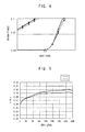
- FIG. 4 is an enlarged view of a graph showing a gray level in relation to a transmissive rate according to an exemplary embodiment of the present invention;
- FIG. 5 is a graph showing color coordinates when viewing from a side of an LCD device according to an exemplary embodiment of the present invention;
- FIG. 6A is a graph showing a conventional gamma curve;
- FIG. 6B is a graph showing a setting of a high pixel target gamma curve and a low pixel target gamma curve;
- FIG. 6C is a graph showing an extracting operation of gradation data corresponding to a luminance that is approximated with the high and low pixel target values from the gamma curve to extract a gamma look-up-table ("LUT") according to an exemplary embodiment of the present invention;
- FIG. 7 is a table for describing an example of each RGB gamma look-up-table (LUT) corresponding to a high pixel and a low pixel that are extracted and set according to an exemplary embodiment of the present invention; and
- FIG. 8 is a block diagram illustrating an LCD device according to an exemplary embodiment of the present invention.
- Exemplary embodiments of the invention are described more fully hereinafter with reference to the accompanying drawings. This invention may, however, be embodied in many different forms and should not be construed as limited to the embodiments set forth herein.
- A super patterned vertical alignment ("SPVA") mode LCD device increases a viewing angle of the LCD device, which has a main pixel and a sub pixel that are formed in a pixel area of the LCD device. Each of the main pixel and the sub pixel receives a different pixel voltage from each other.
- In the SPVA mode LCD device, each of the main and sub pixels has a different distribution of liquid crystal molecules, so that a side visibility of the SPVA mode LCD device is enhanced.
- However, when the SPVA mode LCD device is observed from a side, a yellowing color can be observed. For example, it can be observed that color coordinate values of each gradation corresponding to a side of the SPVA mode LCD device and that of each gradation corresponding to a front of the SPVA mode LCD device are different from each other.
- FIGS. 1A and 1B are graphs showing a variation of color coordinates when viewing from a front and a side of an SPVA mode LCD device.
- Referring to FIG. 1A, as a gradation varies, an X-color coordinate corresponding to a front of the SPVA mode LCD device is plotted from about 0.265 to about 0.28, and a Y-color coordinate corresponding to a front of the SPVA mode LCD device is plotted from about 0.23 to about 0.288.
- The above description is summarized as following Table 1.
Table 1 gradation 0 32 64 96 128 160 192 224 256 X-color coordinate 0.265 0.270 0.275 0.278 0.280 0.280 0.280 0.280 0.280 Y-color coordinate 0.230 0.260 0.277 0.282 0.285 0.285 0.287 0.287 0.288 - Alternatively, as a gradation varies, an X-color coordinate corresponding to a side of the LCD device is plotted from about 0.27 to about 0.29, and a Y-color coordinate corresponding to a side of the LCD device is plotted from about 0.26 to about 0.3.
- The above description is summarized as following Table 2.
Table 2 Gradation 0 32 64 96 128 160 192 224 256 X-color coordinate 0.278 0.278 0.282 0.290 0.292 0.292 0.290 0.292 0.290 Y-color coordinate 0.260 0.276 0.285 0.295 0.299 0.298 0.296 0.230 0.296 - When Table 1 and Table 2 are compared to each other, a color coordinate value of each of the gradations corresponding to a side of the LCD device is greater than that of each of the gradations corresponding to a front of the LCD device. The relatively high color coordinate value represents that more yellow components are included in the LCD device.
- A color coordinate value of the gradations at a front of the LCD device is different from a color coordinate value of the gradations at a side of the LCD device, due to the difference of each of RGB gamma data.
- FIG. 2A is a graph showing conventional double gamma curves. FIG. 2B is an enlarged view part of 'A' of FIG. 2A according to an exemplary embodiment of the present invention.
- Referring to FIGS. 2A and 2B, RGB gamma data that corresponds to a low pixel gamma curve of the double gamma curves are different from each other. The low pixel gamma curve determines a side visibility of the SPVA mode LCD device. As shown in FIG. 2A, a red gamma curve (RED B), a green gamma curve (GREEN B) and a blue gamma curve (BLUE B) of the low pixel gamma curve are different from each other in a low-gradation, in particular a black-gradation. A difference of the red, green and blue gamma curves induces a color variation at a side of the SPVA mode LCD device.
- FIG. 3 is a block diagram showing an LCD device according to an exemplary embodiment of the present invention.
- Referring to FIG. 3, an
LCD device 100 according to an exemplary embodiment of the present invention includes anLCD panel 110, astoring section 120, atiming controller 130, agate driver 140 and adata driver 150. - The
LCD panel 110 may include high and low pixels that are defined by gate lines adjacent to each other, odd numbered data lines DL and even numbered data lines DL that are adjacent to the odd numbered data lines DL. - The high pixel may include a first switching element Th, a first liquid crystal capacitor Clch and a first storage capacitor Csth. The first switching element Th is electrically connected to one of the gate lines and to an even numbered data line DL. The first liquid crystal capacitor Clch and the first storage capacitor Csth are electrically connected to the first switching element Th.
- The low pixel may include a second switching element TI, a second liquid crystal capacitor Clcl and a second storage capacitor Cstl. The second switching element Tl is electrically connected to a remaining gate line that is adjacent to the gate line connected to the first switching element TI and to an odd numbered data line DL. The second liquid crystal capacitor Clcl and the second storage capacitor Cstl are electrically connected to the second switching element Tl.
- The
storing section 120 may include afirst storing section 122 storing RGB gamma data corresponding to the high pixel and asecond storing section 124 storing RGB gamma data corresponding to the low pixel. - The
first storing section 122 may include a first look-up-table ("LUT") storing R gamma data corresponding to the high pixel, a second look-up-table storing G gamma data corresponding to the high pixel and a third look-up-table storing B gamma data corresponding to the high pixel. - The
second storing section 124 may include a fourth look-up-table ("LUT") storing R gamma data corresponding to the low pixel, a fifth look-up-table storing G gamma data corresponding to the low pixel and a sixth look-up-table storing B gamma data corresponding to the low pixel. Particularly, same RGB gamma data are stored in thesecond storing section 124, as shown in FIG. 4, which corresponds to a low-gradation among the RGB gamma data corresponding to the low pixel. The low-gradation is about 10% of a full-gradation. - The
timing controller 130 receives a first image signal R, G and B and a first timing signal S1 from a host system such as an external graph controller (not shown). The first timing signal S1 may include a horizontal synchronizing signal Hsync, a vertical synchronizing signal Vsync, a data enable signal DE and a main clock signal MCLK. - The horizontal synchronizing signal Hsync represents a time required to display one line of the field. The vertical synchronizing signal Vsync represents a time required to display one frame field. Thus, the horizontal synchronizing signal Hsync includes pulses corresponding to the number of pixels included in one line. The data enable signal DE represents a time required to supply the pixel with data.
- The
timing controller 130 outputs a second image signal RH, GH and BH and a second timing signal S2, which have been processed for the RGB gamma data corresponding to the high pixel. The second timing signal S2 includes a load signal LOAD and a start of horizontal signal STH. - The
timing controller 130 outputs a third image signal RL, GL and BL and a third timing signal S3, which have been processed for the RGB gamma data corresponding to the low pixel. The third timing signal S3 includes a gate clock signal Gate Clk (CPV or GCLK) and a start of vertical signal STV. - The
gate driver 140 outputs gate signals G1, G2, ..., Gq-1 and Gq that activates the gate lines GL in response to the third timing signal S3 outputted from thetiming controller 130. - The
data driver 150 transforms each of the second and third image signals RH, GH, BH, RL, GL and BL into a plurality of data voltages D1, D2, ..., Dp-1 and Dp in response to the second timing signal S2 that is provided from thetiming controller 130, and outputs the transformed data voltages D1, D2, ..., Dp-1 and Dp to the data lines DL, respectively. The data voltages D1, D2, ..., Dp-1 and Dp have a relatively inverting polarity for a polarity of a common voltage Vcom. - When a polarity of the common voltage is a low level, a polarity of the data voltages D1, D2, ..., Dp-1 and Dp is a high level with respect to the common voltage Vcom. Alternatively, when a polarity of the common voltage is a high level, a polarity of the data voltages D1, D2, ..., Dp-1 and Dp is a low level with respect to the common voltage Vcom.
- The
LCD device 100 may include a power generating section (not shown) that provides thegate driver 140 with gate on/off voltages VON/VOFF in response to a fourth timing signal (not shown) provided from thetiming controller 130. - The power generating section provides a common voltage Vcom to the first and second liquid crystal capacitors Clch and Clcl of the
LCD panel 110 in synchronize with the gate signals G1, G2, ..., Gq-1 and Gq. - As described above, a low-gradation of a low pixel gamma curve, particularly a plurality of RGB gamma curves corresponding to a black gradation is matched with each other, so that display defects such as yellowing is prevented, which may be observed at a side of the LCD device, which is generated by differentiating between color coordinates of each gradation at a side viewing and that of each gradation at a front viewing.
- FIG. 5 is a graph showing color coordinates of a side view of an exemplary embodiment of the present invention.
- Referring to FIG. 5, as varying of a gradation, an X-color coordinate corresponding to a side of the LCD device is plotted from about 0.278 to about 0.294, and a Y-color coordinate corresponding to a side of the LCD device is plotted from about 0.26 to about 0.293.
- The above description was summarized as following Table 3.
Table 3 gradation 0 32 64 96 128 160 192 224 256 X-color 0.278 0.276 0.282 0.286 0.289 0.290 0.290 0.294 0.290 Y-color 0.260 0.276 0.282 0.287 0.289 0.290 0.290 0.293 0.290 - When the Table 2 and Table 3 are compared to each other, as varying of a gradation, an X-color coordinate value of each of gradations, which is observed at a side of the LCD device according to an exemplary embodiment of the present invention, is smaller than that of each of gradations, which is observed at a side of the conventional LCD device. Therefore, an occurrence of a yellowish is prevented. The yellowish occurred when an X-color coordinate value corresponding to a side of the LCD is relatively higher than an X-color coordinate value corresponding to a front of the LCD.
- Also, as varying of a gradation, a Y-color coordinate value of each of gradations, which is observed at a side of the LCD device according to an exemplary embodiment of the present invention, is smaller than that of each of gradations that is observed at a side of the conventional LCD device. Therefore, an occurrence of a yellowish is prevented. The yellowish occurred when a Y-color coordinate value corresponding to a side of the LCD is relatively higher than a Y-color coordinate value corresponding to a front of the LCD.
- FIG. 6A is a graph showing a conventional gamma curve. FIG. 6B is a graph showing a setting of a high pixel target gamma curve and a low pixel target gamma curve. FIG. 6C is a graph showing an extracting operation of gradation data corresponding to a luminance, which is approximated with the high and low pixel target values from the conventional gamma curve to extract a gamma look-up-table (LUT) according to an exemplary embodiment of the present invention.
- Referring to FIG. 6A, when a same voltage is applied into each of the high and low pixels of the LCD device, a plurality of luminance data corresponding to gradations are extracted based on the conventional gamma curve. A plurality of bits of the luminance data that correspond to gradations are extended using a dithering method to generate LUTs corresponding to the high pixel and the low pixel, respectively.
- For example, a 90.25-gradation, a 90.5-gradation and a 90.75-gradation are existed between about 90-gradation and about 91-gradation that are defined by 8 bits. When the 90.25-gradation, the 90.5-gradation and the 90.75-gradation are bit-extended using a dithering method, the 90-gradation is transformed into a 360-gradation and the 90.25-gradation is transformed into a 361-gradation. Also, the 90.5-gradation is transformed into a 362-gradation, the 90.75-gradation is transformed into a 363-gradation, and the 91-gradation is transformed into a 364-gradation.
- Referring to FIG. 6B, to optimize a side visibility of the LCD device, a gamma curve (B-TARGET) corresponding to a target low pixel is established, and then a gamma curve (A-TARGET) corresponding to a target high pixel is established in accordance with a front target gamma curve (front-TARGET).
- Referring to FIG. 6C, a gradation value corresponding to a luminance, which is approximated with the target high pixel gamma curve and the target low pixel gamma curve of each gradations, is extracted from the plurality of bit extended conventional gamma data. The extracted gradation values are stored with a look-up-table ("LUT") type.
- When the conventional gamma data is about 128-gradation, a transmittance that is mapped in a gamma curve corresponding to the high pixel is 205.25-gradation in the conventional gamma curve. The 205.25-gradation is 8 bits so that the 205.25-gradation is mapped to 821-gradation through a bit extending process of 10 bits.
- When the conventional gamma data is about 128-gradation, a transmittance that is mapped in a gamma curve corresponding to the low pixel is 66-gradation in the conventional gamma curve. The 66-gradation is 8 bits so that the 66-gradation is mapped to 264-gradation through a bit extending process of 10 bits.
- The above process is independently performed with respect to RGB data, so that a gamma tuning for each of the RGB data is possible.
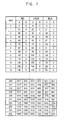
- FIG. 7 is a table for describing one example of each RGB gamma look-up-tables (LUTs) corresponding to a high pixel and a low pixel that are extracted and set in accordance with an exemplary embodiment of the present invention.
- Referring to FIG. 7, a low pixel gamma data (shown in 'A' column) and a high pixel gamma data (shown in 'B' column) that correspond to each RGB of gradations are established.
- RGB gamma data corresponding to a low-gradation of a RGB gamma data corresponding to the high pixel are increased as a gradation is increased. However, RGB gamma data corresponding to a low-gradation of a RGB gamma data corresponding to the low pixel are same even though a gradation is increased.
- In FIG. 7, RGB gamma data corresponding to a low-gradation of RGB gamma data corresponding to a low pixel are '0'. A range of the RGB gamma data corresponding to the low-gradation of the RGB gamma data corresponding to the low-gradation has, for example, about 10% of a full-gradation.
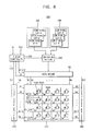
- FIG. 8 is a block diagram illustrating an LCD device according to an exemplary embodiment of the present invention.
- Referring to FIG. 8, an
LCD device 200 according to an exemplary embodiment of the present invention may include anLCD panel 210, afirst storing section 220, asecond storing section 230, atiming controller 250, aswitching section 260, afirst gate driver 270, asecond gate driver 280 and adata driver 290. - The
LCD panel 210 may include a high pixel and a low pixel. The high pixel and the low pixel are formed in a pixel area defined by adjacent gate lines and adjacent data lines. - The high pixel may include a first switching element Th, a first liquid crystal capacitor Clch and a first storage capacitor Csth. The first switching element Th is electrically connected to an even-numbered gate line and an even-numbered data line. The first liquid crystal capacitor Clch and the first storage capacitor Csth are electrically connected to the first switching element Th.
- The low pixel may include a second switching element TI, a second liquid crystal capacitor Clcl and a second storage capacitor Cstl. The second switching element TI is electrically connected to an odd-numbered gate line and an odd-numbered data line. The second liquid crystal capacitor Clcl and the second storage capacitor Cstl are electrically connected to the second switching element TI.
- The
first storing section 220 stores a plurality of gamma data corresponding to the high pixel gamma curves of RGB data, respectively. - The
second storing section 230 stores a plurality of gamma data corresponding to low pixel gamma curves of RGB data, respectively. Particularly, the same RGB gamma data corresponding to a low-gradation are stored in thesecond storing section 230. The low-gradation of the RGB gamma data corresponds to the low pixel. The low-gradation is about 10% of a full-gradation. - The
timing controller 250 provided a first image signal R, G and B and a first timing signal S1 from a host system such as an external graph controller (not shown). The first timing signal S1 may include a horizontal synchronizing signal Hsync, a vertical synchronizing signal Vsync, a data enable signal DE and a main clock signal MCLK. The horizontal synchronizing signal Hsync represents a time required for displaying one line of the field. The vertical synchronizing signal Vsync represents a time required to display one frame field. Thus, the horizontal synchronizing signal Hsync includes pulses corresponding to the number of pixels included in one line. The data enable signal DE represents a time required to supply the pixel with a data. - The
timing controller 250 generates a second image signal R', G' and B' based on the first image signal R, G and B, and then provides thedata driver 290 with the second image signal R', G' and B' and the second timing signal S2. The second timing signal S2 includes a load signal LOAD and a start of horizontal signal STH. - The
switching section 260 provides thedata driver 290 with the gamma data corresponding to the RGB high pixel gamma curves and the gamma data corresponding to the RGB low pixel gamma curves in response to control thetiming controlling section 250. - The
first gate driver 270 provides the even-numbered gate lines GL1, GL3, ..., GLq-3 and GLq-1 of theLCD panel 210 with first gate signals G1, G3, ..., Gq-3 and Gq-1 that activate the even-numbered gate lines GL1, GL3, ..., GLq-3 and GLq-1 in response to a third timing signal S31 that is provided from thetiming controller 250. The third timing signal S31 includes a first gate clock signal Gate Clk1 and a first start of vertical signal STV1. - The
second gate driver 280 provides the odd-numbered gate lines GL2, GL4, ..., GLq-2 and GLq of theLCD panel 210 with second gate signals G2, G4, ..., Gq-2 and Gq that activate the odd-numbered gate lines GL2, GL4, ..., GLq-2 and GLq in response to a fourth timing signal S32 that is provided from thetiming controller 250. The fourth timing signal S32 includes a second gate clock signal Gate Clk2 and a second start of vertical signal STV2. - The
data driver 290 compensates the second image signals R',G' and B' provided from thetiming controller 250 using the RGB gamma data corresponding to the high pixel and the RGB gamma data corresponding to the low pixel in response to the second timing signal S2 that is provided from thetiming controller 250. - The
data driver 290 transforms each of the compensated second image signals R', G', B' into a plurality of data voltages D1, D2, ..., Dp-1 and Dp, and outputs the transformed data voltages D1, D2, ..., Dp-1 and Dp to the data lines DL, respectively. The data voltages D1, D2, ..., Dp-1 and Dp have a relatively inverting polarity for a polarity of a common voltage Vcom. - For example, when a polarity of the common voltage is a low level, a polarity of the data voltages D1, D2, ..., Dp-1 and Dp is a high level with respect to the common voltage Vcom. Alternatively, when a polarity of the common voltage is a high level, a polarity of the data voltages D1, D2, ..., Dp-1 and Dp is a low level with respect to the common voltage Vcom.
- The
LCD device 200 may include a power generating section (not shown) that provides the first andsecond gate drivers timing controller 250. - The power generating section provides a common voltage Vcom to the first and second liquid crystal capacitors Clch and Clcl of the
LCD panel 210 in synchronize with the gate signals G1, G2, ..., Gq-1 and Gq. - As described above, in the LCD device having two sub-pixels corresponding to two gamma curves, respectively, that are the high pixel gamma curve and the low pixel gamma curve, corresponding to two sub-pixels to enhance a visibility of the LCD device, RGB gamma data corresponding to each high and low pixels is independently controlled, so that it is prevented from being a difference of a color coordinate value of gradations.
- Particularly, each of RGB gamma curves corresponding to a low-gradation of the low pixel gamma curve are matched, so that a yellowish that is observed at a side of the LCD device is removed, which is due to a difference of a color coordinate value of gradations of the side and front of the LCD device. Therefore, it is prevented from occuring a display error.
- Although the exemplary embodiments of the present invention have been described herein with reference to the accompanying drawings, it is to be understood that the present invention should not be limited to those precise embodiments and that various other changes and modifications can be affected therein by one ordinary skilled in the related art without departing from the scope or spirit of the invention. All such changes and modifications are intended to be included within the scope of the invention as defined by the appended claims.
Claims (15)
- A display device comprising:a display panel having a high pixel and a low pixel, wherein the high pixel and the low pixel are formed in a pixel area; anda driving section receiving a first image signal from an external device, outputting a second image signal to the high pixel by using gamma data that corresponds to a high pixel gamma curve, and outputting a third image signal to the low pixel by using gamma data that corresponds to a low pixel gamma curve,wherein the driving section outputs the third image signal to the low pixel by using the same gamma data for each of RGB data that corresponds to a low gradation of the low pixel gamma curve.
- The display device of claim 1, wherein the driving section comprises:a timing controller generating the second and third image signals based on the first image signal;a gate driver outputting a plurality of gate signals to activate a plurality of gate lines; anda data driver compensating the second image signal that is provided from the timing controller by using the gamma data that corresponds to the high pixel gamma curve, compensating the third image signal that is provided from the timing controller by using the gamma data that corresponds to the low pixel gamma curve, and outputting the compensated second and third image signals to the display panel.
- The display device of claim 2, further comprising a storing section storing the RGB gamma data corresponding to the high pixel and the RGB data corresponding to the low pixel,
wherein the timing controller generates the second image signal by using the RGB gamma data corresponding to the high pixel, and generates the third image signal by using the RGB data corresponding to the low pixel. - The display device of claim 2, wherein the pixel area is defined by two adjacent gate lines, an odd numbered data line and an even numbered data line that is adjacent to the odd numbered data line.
- The display device of claim 4, wherein the high pixel comprises:a switching element electrically connected to one gate line of the two adjacent gate lines and to the even numbered data line; anda liquid crystal capacitor electrically connected to the switching element.
- The display device of claim 5, wherein the low pixel comprises:a switching element electrically connected to a remaining gate line of the two adjacent gate lines and to the odd numbered data line; anda liquid crystal capacitor electrically connected to the switching element.
- The display device of claim 1, wherein the driving section comprises:a timing controller generating the second image signal based on the first image signal;a first gate driver outputting a plurality of gate signals to activate even-numbered gate lines;a second gate driver outputting a plurality of gate signals to activate odd-numbered gate lines; anda data driver outputting the second image signal provided from the timing controller to the display panel.
- The display device of claim 7, further comprising a storing section storing a high RGB gamma data corresponding to the high pixel and a low RGB gamma data corresponding to the low pixel,
wherein the driving section further comprises a switching section outputting the high RGB gamma data and the low RGB gamma data to the data driver in response to a controlling of the timing controller. - The display device of claim 8, wherein the data driver compensates the second image signal using the high RGB gamma data and the low RGB gamma data, and outputs the compensated high RGB gamma data and the compensated low RGB gamma data to the display panel.
- The display device of claim 9, wherein the pixel area is defined by two adjacent gate lines and adjacent two data lines,
the high pixel comprises,
a first switching element electrically connected to an even-numbered gate line corresponding to the first gate driver; and
a first liquid crystal capacitor electrically connected to the first switching element. - The display device of claim 10, wherein the low pixel comprises:a second switching element electrically connected to an odd-numbered gate line corresponding to the second gate driver; anda second liquid crystal capacitor electrically connected to the second switching element.
- A display device comprising:a display panel having a high pixel and a low pixel that are formed in a pixel area;a storing section storing high RGB gamma data corresponding to the high pixel and low RGB gamma data corresponding to the low pixel;a timing controller receiving a first image signal from an external device, outputting a second image signal adapted the first image signal to the high RGB gamma data, and outputting a third image signal adapted the first image signal to the low RGB gamma data;a gate driver outputting a gate signal to activate the gate line in response to controlling of the timing controller; anda data driver outputting the second and third image signals to the data line in response to the controlling of the timing controller,wherein the storing section stores same RGB gamma data, which corresponds to a low-gradation of the low RGB gamma data.
- The display device of claim 12, wherein the low gradation is about 10% of a full-gradation.
- A display device comprising:a display panel having high and low pixels that are formed in a pixel area;a first storing section storing high RGB gamma data corresponding to high pixel gamma curves of RGB data, respectively;a second storing section storing low RGB gamma data corresponding to low pixel gamma curves of RGB data, respectively;a timing controller receiving a first image signal from an external device and generating a second image signal based on the first image signal;a switching section selectively outputting the high RGB gamma data and the low RGB gamma data in response to controlling of the timing controller;a first gate driver outputting a first gate signal to activate an even-numbered gate line of the display panel;a second gate driver outputting a second gate signal to activate an odd-numbered gate line of the display panel; anda data driver compensating the second image signal using the high RGB gamma data and the low RGB gamma data, and outputting the compensated second image signal to the display panel,wherein the second storing section stores the same RGB gamma data corresponding to a low-gradation of the low RGB gamma data.
- The display device of claim 14, wherein the low gradation is about 10% of a full-gradation.
Applications Claiming Priority (1)
| Application Number | Priority Date | Filing Date | Title |
|---|---|---|---|
| KR1020060017511A KR101206724B1 (en) | 2006-02-23 | 2006-02-23 | Display apparatus |
Publications (3)
| Publication Number | Publication Date |
|---|---|
| EP1826746A2 true EP1826746A2 (en) | 2007-08-29 |
| EP1826746A3 EP1826746A3 (en) | 2009-04-22 |
| EP1826746B1 EP1826746B1 (en) | 2014-01-15 |
Family
ID=38066410
Family Applications (1)
| Application Number | Title | Priority Date | Filing Date |
|---|---|---|---|
| EP07002020.1A Active EP1826746B1 (en) | 2006-02-23 | 2007-01-31 | Liquid crystal display device |
Country Status (5)
| Country | Link |
|---|---|
| US (1) | US7973751B2 (en) |
| EP (1) | EP1826746B1 (en) |
| JP (1) | JP5021334B2 (en) |
| KR (1) | KR101206724B1 (en) |
| CN (1) | CN101025494B (en) |
Cited By (1)
| Publication number | Priority date | Publication date | Assignee | Title |
|---|---|---|---|---|
| US8581823B2 (en) | 2007-12-28 | 2013-11-12 | Lg Display Co., Ltd. | Liquid crystal display device and driving method thereof |
Families Citing this family (31)
| Publication number | Priority date | Publication date | Assignee | Title |
|---|---|---|---|---|
| US8654050B2 (en) * | 2007-09-13 | 2014-02-18 | Sharp Kabushiki Kaisha | Multiple-primary-color liquid crystal display device |
| JP5312779B2 (en) * | 2007-12-13 | 2013-10-09 | ルネサスエレクトロニクス株式会社 | Liquid crystal display device, data driving IC, and liquid crystal display panel driving method |
| JP5289757B2 (en) * | 2007-12-13 | 2013-09-11 | ルネサスエレクトロニクス株式会社 | Liquid crystal display device, data driving IC, and liquid crystal display panel driving method |
| KR101461024B1 (en) * | 2008-03-06 | 2014-11-13 | 삼성디스플레이 주식회사 | A driving method of a display panel, a driving device for performing the same, and a display device including the driving device |
| TWI399719B (en) | 2008-08-07 | 2013-06-21 | Innolux Corp | Display device and display method thereof |
| CN101739969B (en) * | 2008-11-24 | 2013-07-24 | 群创光电股份有限公司 | Display device and display method thereof |
| CN102227675B (en) * | 2008-11-28 | 2014-05-28 | 夏普株式会社 | Multiple primary color liquid crystal display device and signal conversion circuit |
| JP5680969B2 (en) | 2008-12-26 | 2015-03-04 | シャープ株式会社 | Liquid crystal display |
| US8576262B2 (en) | 2008-12-26 | 2013-11-05 | Sharp Kabushiki Kaisha | Liquid crystal display apparatus |
| CN101930715B (en) * | 2009-06-18 | 2013-11-20 | 群康科技(深圳)有限公司 | Gray-insertion drive circuit and method thereof |
| JPWO2011010637A1 (en) * | 2009-07-22 | 2012-12-27 | シャープ株式会社 | Manufacturing method of liquid crystal display device |
| US20140118423A1 (en) * | 2011-06-27 | 2014-05-01 | Sharp Kabushiki Kaisha | Liquid crystal display apparatus |
| JP5144838B1 (en) * | 2011-11-29 | 2013-02-13 | パナソニック株式会社 | Information processing apparatus, information processing method, and program |
| KR102087411B1 (en) * | 2013-08-01 | 2020-04-16 | 삼성디스플레이 주식회사 | Display apparatus and driving method thereof |
| TWI497470B (en) * | 2013-11-12 | 2015-08-21 | Au Optronics Corp | Display panel driving method and display panel |
| CN104361870B (en) * | 2014-11-05 | 2017-07-28 | 深圳市华星光电技术有限公司 | Liquid crystal panel and its pixel cell establishing method |
| CN104317084B (en) * | 2014-11-07 | 2017-05-17 | 深圳市华星光电技术有限公司 | Liquid crystal panel and driving method thereof |
| CN104299592B (en) * | 2014-11-07 | 2016-11-23 | 深圳市华星光电技术有限公司 | Liquid crystal panel and driving method thereof |
| CN104835468B (en) * | 2015-05-21 | 2018-02-13 | 深圳市华星光电技术有限公司 | Liquid crystal panel and its driving method |
| CN104900203B (en) * | 2015-06-11 | 2017-05-17 | 深圳市华星光电技术有限公司 | Liquid-crystal panel and drive method therefor |
| CN104900205B (en) * | 2015-06-12 | 2017-04-26 | 深圳市华星光电技术有限公司 | Liquid-crystal panel and drive method therefor |
| CN104952412B (en) * | 2015-07-15 | 2018-04-13 | 深圳市华星光电技术有限公司 | The driving method and driving device of liquid crystal panel |
| US10325543B2 (en) | 2015-12-15 | 2019-06-18 | a.u. Vista Inc. | Multi-mode multi-domain vertical alignment liquid crystal display and method thereof |
| CN107886896B (en) * | 2017-11-03 | 2019-08-23 | 惠科股份有限公司 | three-color and four-color pixel display panel compatible system and method |
| CN107945758A (en) * | 2017-12-31 | 2018-04-20 | 深圳市华星光电半导体显示技术有限公司 | The driving method and display device of a kind of display panel |
| KR102521898B1 (en) * | 2018-06-28 | 2023-04-18 | 삼성디스플레이 주식회사 | Display device capable of changing frame rate and driving method thereof |
| US11011095B2 (en) * | 2018-08-31 | 2021-05-18 | Chongqing Hkc Optoelectronics Technology Co., Ltd. | Display panel, and image control device and method thereof |
| KR102732236B1 (en) * | 2019-04-17 | 2024-11-21 | 삼성디스플레이 주식회사 | Display device including a plurality of data drivers |
| KR20230145633A (en) | 2022-04-08 | 2023-10-18 | 삼성디스플레이 주식회사 | Method of correcting gamma of the display device |
| TWI796265B (en) * | 2022-07-27 | 2023-03-11 | 友達光電股份有限公司 | Display apparatus and image displaying method |
| KR20240130837A (en) | 2023-02-22 | 2024-08-30 | 삼성디스플레이 주식회사 | Display device, and method of operating a display device |
Family Cites Families (20)
| Publication number | Priority date | Publication date | Assignee | Title |
|---|---|---|---|---|
| JP3202450B2 (en) * | 1993-10-20 | 2001-08-27 | 日本電気株式会社 | Liquid crystal display |
| JP3184069B2 (en) * | 1994-09-02 | 2001-07-09 | シャープ株式会社 | Image display device |
| JP2002229505A (en) * | 2001-01-31 | 2002-08-16 | Nec Corp | Display device |
| JP2003050566A (en) * | 2001-08-06 | 2003-02-21 | Nec Corp | Liquid crystal display |
| US7119770B2 (en) * | 2001-08-17 | 2006-10-10 | Lg Electronics Inc. | Driving apparatus of electroluminescent display device and driving method thereof |
| KR100803163B1 (en) * | 2001-09-03 | 2008-02-14 | 삼성전자주식회사 | LCD Display |
| KR100841616B1 (en) * | 2001-12-31 | 2008-06-27 | 엘지디스플레이 주식회사 | Driving device of liquid crystal panel |
| JP3999081B2 (en) * | 2002-01-30 | 2007-10-31 | シャープ株式会社 | Liquid crystal display |
| JP4044347B2 (en) * | 2002-03-05 | 2008-02-06 | 松下電器産業株式会社 | Driving method of liquid crystal display device |
| JP4342200B2 (en) * | 2002-06-06 | 2009-10-14 | シャープ株式会社 | Liquid crystal display |
| KR100890022B1 (en) * | 2002-07-19 | 2009-03-25 | 삼성전자주식회사 | LCD and its driving method |
| JP2003308057A (en) * | 2003-03-17 | 2003-10-31 | Sharp Corp | Color display |
| JP4413515B2 (en) * | 2003-03-31 | 2010-02-10 | シャープ株式会社 | Image processing method and liquid crystal display device using the same |
| KR100945581B1 (en) | 2003-06-23 | 2010-03-08 | 삼성전자주식회사 | LCD and its driving method |
| TWI285870B (en) * | 2003-08-27 | 2007-08-21 | Chi Mei Optoelectronics Corp | Liquid crystal display and driving method |
| JP2005222327A (en) * | 2004-02-05 | 2005-08-18 | Sony Corp | Color signal processing device and display device |
| JP4394512B2 (en) * | 2004-04-30 | 2010-01-06 | 富士通株式会社 | Liquid crystal display device with improved viewing angle characteristics |
| JP2005352483A (en) | 2004-06-09 | 2005-12-22 | Samsung Electronics Co Ltd | Liquid crystal display device and driving method thereof |
| KR101039025B1 (en) | 2004-06-25 | 2011-06-03 | 삼성전자주식회사 | Display device, drive device for display device and driving method |
| TWI253054B (en) * | 2004-10-29 | 2006-04-11 | Chi Mei Optoelectronics Corp | Color display |
-
2006
- 2006-02-23 KR KR1020060017511A patent/KR101206724B1/en not_active Expired - Lifetime
-
2007
- 2007-01-16 US US11/623,512 patent/US7973751B2/en active Active
- 2007-01-31 EP EP07002020.1A patent/EP1826746B1/en active Active
- 2007-02-15 CN CN2007100793569A patent/CN101025494B/en active Active
- 2007-02-22 JP JP2007042515A patent/JP5021334B2/en active Active
Cited By (2)
| Publication number | Priority date | Publication date | Assignee | Title |
|---|---|---|---|---|
| US8581823B2 (en) | 2007-12-28 | 2013-11-12 | Lg Display Co., Ltd. | Liquid crystal display device and driving method thereof |
| DE102008033127B4 (en) | 2007-12-28 | 2020-04-23 | Lg Display Co., Ltd. | Liquid crystal display device and driving method thereof |
Also Published As
| Publication number | Publication date |
|---|---|
| KR101206724B1 (en) | 2012-11-30 |
| KR20070087288A (en) | 2007-08-28 |
| EP1826746B1 (en) | 2014-01-15 |
| EP1826746A3 (en) | 2009-04-22 |
| US20080036718A1 (en) | 2008-02-14 |
| JP5021334B2 (en) | 2012-09-05 |
| CN101025494B (en) | 2012-12-05 |
| US7973751B2 (en) | 2011-07-05 |
| CN101025494A (en) | 2007-08-29 |
| JP2007226242A (en) | 2007-09-06 |
Similar Documents
| Publication | Publication Date | Title |
|---|---|---|
| EP1826746B1 (en) | Liquid crystal display device | |
| US8896510B2 (en) | Display device and driving method therefor | |
| JP4953227B2 (en) | Display device having gate drive unit | |
| US7898536B2 (en) | Display apparatus and method of driving the same | |
| US8963965B2 (en) | Method for generating data for driving a display panel, data driving circuit for performing the same and display device having the data driving circuit | |
| EP2192572B1 (en) | Method for driving display panel and display apparatus for performing the method | |
| US9697783B2 (en) | Display apparatus and method of driving the display apparatus | |
| JP2006215572A (en) | Display device and driving method thereof | |
| US20150170598A1 (en) | Method of driving display panel and display apparatus for performing the same | |
| CN1901020B (en) | Liquid crystal display and its driving method | |
| US20060038759A1 (en) | Liquid crystal display and driving method thereof | |
| CN101127195A (en) | Common voltage compensation device, liquid crystal display and driving method thereof | |
| KR102198250B1 (en) | Display apparatus and driving method thereof | |
| US20150379952A1 (en) | Display device | |
| US8207927B2 (en) | Liquid crystal display and method of operating the same | |
| KR20070048514A (en) | Liquid crystal display and method for driving there of | |
| US8884860B2 (en) | Liquid crystal display having increased response speed, and device and method for modifying image signal to provide increased response speed | |
| US9842553B2 (en) | Method of driving display panel and display apparatus for performing the same | |
| EP1868179A2 (en) | Signal processing device, liquid crystal display having the same and method of manufactuirng the same | |
| US9292942B2 (en) | Image signal compensation apparatus and liquid crystal display including the same | |
| US8354977B2 (en) | Driving method for solving problem of cross talk effect of display panel | |
| KR20130018025A (en) | Signal processing unit and liquid crystal display device comprising the same | |
| KR100900547B1 (en) | Driving device of liquid crystal display | |
| KR20070082769A (en) | Liquid crystal display |
Legal Events
| Date | Code | Title | Description |
|---|---|---|---|
| PUAI | Public reference made under article 153(3) epc to a published international application that has entered the european phase |
Free format text: ORIGINAL CODE: 0009012 |
|
| 17P | Request for examination filed |
Effective date: 20070131 |
|
| AK | Designated contracting states |
Kind code of ref document: A2 Designated state(s): AT BE BG CH CY CZ DE DK EE ES FI FR GB GR HU IE IS IT LI LT LU LV MC NL PL PT RO SE SI SK TR |
|
| AX | Request for extension of the european patent |
Extension state: AL BA HR MK YU |
|
| PUAL | Search report despatched |
Free format text: ORIGINAL CODE: 0009013 |
|
| AK | Designated contracting states |
Kind code of ref document: A3 Designated state(s): AT BE BG CH CY CZ DE DK EE ES FI FR GB GR HU IE IS IT LI LT LU LV MC NL PL PT RO SE SI SK TR |
|
| AX | Request for extension of the european patent |
Extension state: AL BA HR MK RS |
|
| AKX | Designation fees paid |
Designated state(s): DE FR GB |
|
| 17Q | First examination report despatched |
Effective date: 20100531 |
|
| RAP1 | Party data changed (applicant data changed or rights of an application transferred) |
Owner name: SAMSUNG ELECTRONICS CO., LTD. |
|
| RAP1 | Party data changed (applicant data changed or rights of an application transferred) |
Owner name: SAMSUNG DISPLAY CO., LTD. |
|
| GRAP | Despatch of communication of intention to grant a patent |
Free format text: ORIGINAL CODE: EPIDOSNIGR1 |
|
| RIC1 | Information provided on ipc code assigned before grant |
Ipc: G09G 3/36 20060101AFI20130722BHEP Ipc: G09G 5/06 20060101ALN20130722BHEP |
|
| INTG | Intention to grant announced |
Effective date: 20130808 |
|
| GRAS | Grant fee paid |
Free format text: ORIGINAL CODE: EPIDOSNIGR3 |
|
| GRAA | (expected) grant |
Free format text: ORIGINAL CODE: 0009210 |
|
| AK | Designated contracting states |
Kind code of ref document: B1 Designated state(s): DE FR GB |
|
| REG | Reference to a national code |
Ref country code: GB Ref legal event code: FG4D |
|
| REG | Reference to a national code |
Ref country code: DE Ref legal event code: R096 Ref document number: 602007034755 Country of ref document: DE Effective date: 20140220 |
|
| REG | Reference to a national code |
Ref country code: DE Ref legal event code: R097 Ref document number: 602007034755 Country of ref document: DE |
|
| PLBE | No opposition filed within time limit |
Free format text: ORIGINAL CODE: 0009261 |
|
| STAA | Information on the status of an ep patent application or granted ep patent |
Free format text: STATUS: NO OPPOSITION FILED WITHIN TIME LIMIT |
|
| 26N | No opposition filed |
Effective date: 20141016 |
|
| REG | Reference to a national code |
Ref country code: DE Ref legal event code: R097 Ref document number: 602007034755 Country of ref document: DE Effective date: 20141016 |
|
| REG | Reference to a national code |
Ref country code: FR Ref legal event code: PLFP Year of fee payment: 10 |
|
| REG | Reference to a national code |
Ref country code: FR Ref legal event code: PLFP Year of fee payment: 11 |
|
| REG | Reference to a national code |
Ref country code: FR Ref legal event code: PLFP Year of fee payment: 12 |
|
| P01 | Opt-out of the competence of the unified patent court (upc) registered |
Effective date: 20230515 |
|
| PGFP | Annual fee paid to national office [announced via postgrant information from national office to epo] |
Ref country code: GB Payment date: 20251222 Year of fee payment: 20 |
|
| PGFP | Annual fee paid to national office [announced via postgrant information from national office to epo] |
Ref country code: FR Payment date: 20251223 Year of fee payment: 20 |
|
| PGFP | Annual fee paid to national office [announced via postgrant information from national office to epo] |
Ref country code: DE Payment date: 20251222 Year of fee payment: 20 |