EP1821339A1 - GaN crystal substrate and method of manufacturing the same, and method of manufacturing semiconductor device - Google Patents
GaN crystal substrate and method of manufacturing the same, and method of manufacturing semiconductor device Download PDFInfo
- Publication number
- EP1821339A1 EP1821339A1 EP07000261A EP07000261A EP1821339A1 EP 1821339 A1 EP1821339 A1 EP 1821339A1 EP 07000261 A EP07000261 A EP 07000261A EP 07000261 A EP07000261 A EP 07000261A EP 1821339 A1 EP1821339 A1 EP 1821339A1
- Authority
- EP
- European Patent Office
- Prior art keywords
- gan crystal
- crystal substrate
- substrate
- rear surface
- warpage
- Prior art date
- Legal status (The legal status is an assumption and is not a legal conclusion. Google has not performed a legal analysis and makes no representation as to the accuracy of the status listed.)
- Granted
Links
Images



Classifications
-
- C—CHEMISTRY; METALLURGY
- C30—CRYSTAL GROWTH
- C30B—SINGLE-CRYSTAL GROWTH; UNIDIRECTIONAL SOLIDIFICATION OF EUTECTIC MATERIAL OR UNIDIRECTIONAL DEMIXING OF EUTECTOID MATERIAL; REFINING BY ZONE-MELTING OF MATERIAL; PRODUCTION OF A HOMOGENEOUS POLYCRYSTALLINE MATERIAL WITH DEFINED STRUCTURE; SINGLE CRYSTALS OR HOMOGENEOUS POLYCRYSTALLINE MATERIAL WITH DEFINED STRUCTURE; AFTER-TREATMENT OF SINGLE CRYSTALS OR A HOMOGENEOUS POLYCRYSTALLINE MATERIAL WITH DEFINED STRUCTURE; APPARATUS THEREFOR
- C30B25/00—Single-crystal growth by chemical reaction of reactive gases, e.g. chemical vapour-deposition growth
- C30B25/02—Epitaxial-layer growth
- C30B25/18—Epitaxial-layer growth characterised by the substrate
- C30B25/20—Epitaxial-layer growth characterised by the substrate the substrate being of the same materials as the epitaxial layer
-
- H—ELECTRICITY
- H10—SEMICONDUCTOR DEVICES; ELECTRIC SOLID-STATE DEVICES NOT OTHERWISE PROVIDED FOR
- H10P—GENERIC PROCESSES OR APPARATUS FOR THE MANUFACTURE OR TREATMENT OF DEVICES COVERED BY CLASS H10
- H10P14/00—Formation of materials, e.g. in the shape of layers or pillars
- H10P14/20—Formation of materials, e.g. in the shape of layers or pillars of semiconductor materials
-
- C—CHEMISTRY; METALLURGY
- C30—CRYSTAL GROWTH
- C30B—SINGLE-CRYSTAL GROWTH; UNIDIRECTIONAL SOLIDIFICATION OF EUTECTIC MATERIAL OR UNIDIRECTIONAL DEMIXING OF EUTECTOID MATERIAL; REFINING BY ZONE-MELTING OF MATERIAL; PRODUCTION OF A HOMOGENEOUS POLYCRYSTALLINE MATERIAL WITH DEFINED STRUCTURE; SINGLE CRYSTALS OR HOMOGENEOUS POLYCRYSTALLINE MATERIAL WITH DEFINED STRUCTURE; AFTER-TREATMENT OF SINGLE CRYSTALS OR A HOMOGENEOUS POLYCRYSTALLINE MATERIAL WITH DEFINED STRUCTURE; APPARATUS THEREFOR
- C30B29/00—Single crystals or homogeneous polycrystalline material with defined structure characterised by the material or by their shape
- C30B29/10—Inorganic compounds or compositions
- C30B29/40—AIIIBV compounds wherein A is B, Al, Ga, In or Tl and B is N, P, As, Sb or Bi
-
- G—PHYSICS
- G01—MEASURING; TESTING
- G01B—MEASURING LENGTH, THICKNESS OR SIMILAR LINEAR DIMENSIONS; MEASURING ANGLES; MEASURING AREAS; MEASURING IRREGULARITIES OF SURFACES OR CONTOURS
- G01B11/00—Measuring arrangements characterised by the use of optical techniques
- G01B11/30—Measuring arrangements characterised by the use of optical techniques for measuring roughness or irregularity of surfaces
-
- H—ELECTRICITY
- H10—SEMICONDUCTOR DEVICES; ELECTRIC SOLID-STATE DEVICES NOT OTHERWISE PROVIDED FOR
- H10P—GENERIC PROCESSES OR APPARATUS FOR THE MANUFACTURE OR TREATMENT OF DEVICES COVERED BY CLASS H10
- H10P50/00—Etching of wafers, substrates or parts of devices
- H10P50/60—Wet etching
- H10P50/64—Wet etching of semiconductor materials
- H10P50/642—Chemical etching
- H10P50/646—Chemical etching of Group III-V materials
-
- H—ELECTRICITY
- H10—SEMICONDUCTOR DEVICES; ELECTRIC SOLID-STATE DEVICES NOT OTHERWISE PROVIDED FOR
- H10P—GENERIC PROCESSES OR APPARATUS FOR THE MANUFACTURE OR TREATMENT OF DEVICES COVERED BY CLASS H10
- H10P50/00—Etching of wafers, substrates or parts of devices
- H10P50/60—Wet etching
- H10P50/64—Wet etching of semiconductor materials
- H10P50/642—Chemical etching
- H10P50/646—Chemical etching of Group III-V materials
- H10P50/648—Anisotropic liquid etching
-
- H—ELECTRICITY
- H10—SEMICONDUCTOR DEVICES; ELECTRIC SOLID-STATE DEVICES NOT OTHERWISE PROVIDED FOR
- H10P—GENERIC PROCESSES OR APPARATUS FOR THE MANUFACTURE OR TREATMENT OF DEVICES COVERED BY CLASS H10
- H10P90/00—Preparation of wafers not covered by a single main group of this subclass, e.g. wafer reinforcement
- H10P90/12—Preparing bulk and homogeneous wafers
-
- H—ELECTRICITY
- H10—SEMICONDUCTOR DEVICES; ELECTRIC SOLID-STATE DEVICES NOT OTHERWISE PROVIDED FOR
- H10P—GENERIC PROCESSES OR APPARATUS FOR THE MANUFACTURE OR TREATMENT OF DEVICES COVERED BY CLASS H10
- H10P90/00—Preparation of wafers not covered by a single main group of this subclass, e.g. wafer reinforcement
- H10P90/12—Preparing bulk and homogeneous wafers
- H10P90/126—Preparing bulk and homogeneous wafers by chemical etching
-
- H—ELECTRICITY
- H10—SEMICONDUCTOR DEVICES; ELECTRIC SOLID-STATE DEVICES NOT OTHERWISE PROVIDED FOR
- H10P—GENERIC PROCESSES OR APPARATUS FOR THE MANUFACTURE OR TREATMENT OF DEVICES COVERED BY CLASS H10
- H10P90/00—Preparation of wafers not covered by a single main group of this subclass, e.g. wafer reinforcement
- H10P90/12—Preparing bulk and homogeneous wafers
- H10P90/129—Preparing bulk and homogeneous wafers by polishing
-
- H—ELECTRICITY
- H10—SEMICONDUCTOR DEVICES; ELECTRIC SOLID-STATE DEVICES NOT OTHERWISE PROVIDED FOR
- H10H—INORGANIC LIGHT-EMITTING SEMICONDUCTOR DEVICES HAVING POTENTIAL BARRIERS
- H10H20/00—Individual inorganic light-emitting semiconductor devices having potential barriers, e.g. light-emitting diodes [LED]
- H10H20/01—Manufacture or treatment
- H10H20/011—Manufacture or treatment of bodies, e.g. forming semiconductor layers
- H10H20/013—Manufacture or treatment of bodies, e.g. forming semiconductor layers having light-emitting regions comprising only Group III-V materials
- H10H20/0137—Manufacture or treatment of bodies, e.g. forming semiconductor layers having light-emitting regions comprising only Group III-V materials the light-emitting regions comprising nitride materials
Definitions
- the present invention relates to a GaN crystal substrate used in a semiconductor device such as a light emitting element, an electronic element, or a semiconductor sensor, a method of manufacturing the same, and a method of manufacturing a semiconductor device for which the GaN crystal substrate is selected as a substrate.
- a GaN crystal substrate is very useful as a substrate for a semiconductor device such as a light emitting element, an electronic element, or a semiconductor sensor.
- a GaN crystal substrate is formed by cutting a GaN crystal grown by vapor phase epitaxy such as HVPE (hydride vapor phase epitaxy) or MOVPE (metalorganic vapor phase epitaxy) into substrates of a predetermined shape, and grinding, lapping, and/or etching a main surface thereof.
- vapor phase epitaxy such as HVPE (hydride vapor phase epitaxy) or MOVPE (metalorganic vapor phase epitaxy)
- One object of the present invention is to provide a GaN crystal substrate having a rear surface with a reduced warpage and allowing a semiconductor layer having good crystallinity to be formed on a crystal growth surface thereof, a method of manufacturing the same, and a method of manufacturing a semiconductor device.
- the present invention is a GaN crystal substrate having a crystal growth surface and a rear surface opposite to the crystal growth surface, the rear surface having a warpage w (R) satisfying -50 ⁇ m ⁇ w (R) ⁇ 50 ⁇ m.
- the rear surface can have a surface roughness Ra (R) satisfying Ra (R) ⁇ 10 ⁇ m. Further, the rear surface can have a surface roughness Ry (R) satisfying Ry (R) ⁇ 75 ⁇ m. Furthermore, the crystal growth surface can have a warpage w (C) satisfying -50 ⁇ m ⁇ w (C) ⁇ 50 ⁇ m, a surface roughness Ra (C) satisfying Ra (C) ⁇ 10 nm, and a surface roughness Ry (C) satisfying Ry (C) ⁇ 60 nm.
- the present invention is a method of manufacturing the GaN crystal substrate described above, including the steps of cutting the GaN crystal substrate out of a grown GaN crystal, and processing the rear surface of the GaN crystal substrate, wherein the step of processing the rear surface of the GaN crystal substrate includes at least one of the steps of grinding the rear surface, lapping the rear surface, and etching the rear surface.
- the present invention is a method of manufacturing a semiconductor device, including the step of preparing the GaN crystal substrate described above as a substrate, and growing at least one group-III nitride crystal layer on a side of the crystal growth surface of the GaN crystal substrate.
- a GaN crystal substrate having a rear surface with a reduced warpage and allowing a semiconductor layer having good crystallinity to be formed on a crystal growth surface thereof, a method of manufacturing the same, and a method of manufacturing a semiconductor device can be provided.
- a rear surface 10r opposite to a crystal growth surface 10c has a warpage w (R) satisfying -50 ⁇ m ⁇ w (R) ⁇ 50 ⁇ m, where a warpage causing rear surface 10r to be concavely curved as shown in Fig. 1A is indicated with a positive (+) sign, and a warpage causing rear surface 10r to be convexly curved as shown in Fig. 1B is indicated with a negative (-) sign.
- Warpage w (R) is defined as a difference in height between a displacement value z P at the most convex portion and a displacement value z v at the most concave portion of rear surface 10r.
- a gap portion 9s formed between a GaN crystal substrate 10 and a susceptor 9 is increased.
- semiconductor layer 20 cannot be grown evenly and stably, which makes it difficult to manufacture a semiconductor device formed evenly and having excellent properties.
- rear surface 10r has warpage w (R) satisfying -35 ⁇ m ⁇ w (R) ⁇ 45 ⁇ m.
- gap portion 9s formed between rear surface 10r and a surface of susceptor 9 is a closed space as shown in Fig. 1A.
- gap portion 9s formed between rear surface 10r and the surface of susceptor 9 is an open space as shown in Fig. 1B.
- heat distribution in the substrate when the warpage is indicated with a positive (+) sign is smaller than heat distribution in the substrate when the warpage indicated with a negative (-) sign. It is contemplated that a preferable range of the warpage is larger on a positive (+) side than on a negative (-) side.
- the warpage of rear surface 10r of the substrate was measured by a method for accurately measuring the warpage of rear surface 10r described below.
- the measurement method is a method of measuring warpage of a rear surface opposite to a crystal growth surface of a substrate using a laser displacement meter, and the substrate is disposed on a substrate support table.
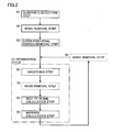
- the method includes: a substrate detection step S 1 detecting a plurality of displacement values respectively corresponding to a plurality of measurement points on the rear surface of the substrate using the laser displacement meter; a noise removal step S2 removing noise contained in the plurality of displacement values; an outer peripheral portion removal step S3 calculating a plurality of displacement values for calculation by removing from the plurality of displacement values those respectively corresponding to the measurement points in an outer peripheral portion of the substrate; a smoothing step S4 smoothing the plurality of displacement values for calculation to calculate a warped surface; a best fit plane calculation step S5 calculating a best fit plane having the minimum distance to the warped surface; and a warpage calculation step S6 calculating as warpage a sum of a distance from the best fit plane to a point represented by the greatest displacement value of the warped surface on one side with respect to the best fit plane and a distance from the best fit plane to a point represented by the greatest displacement value of the warped surface on the other side with respect to the best fit plane.
- the warpage of the rear surface of the substrate can be measured.
- surface roughness Ra is a value obtained by sampling a portion having a reference length from a roughness curve in a direction of its mean line, summing up absolute values of deviations from a mean line of the sampled portion to a measurement curve, and calculating an average for the reference length.
- the step surrounded with a solid frame is an indispensable step
- the step surrounded with a dashed frame is an arbitrary step.
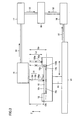
- a laser displacement meter 15 is an apparatus measuring a displacement of rear surface 10r of the substrate (GaN crystal substrate 10) by applying a laser beam 31 on rear surface 10r of the substrate (GaN crystal substrate 10).
- the type of the laser and for example a red color semiconductor laser having a wavelength of 670 nm is used.
- the measuring technique and for example a laser focus technique is used.
- a laser displacement meter employing the laser focus technique has a lower accuracy than a flatness tester employing optical interferometry, it can measure a rough rear surface with surface roughness Ra of not less than 50 nm.
- the laser displacement meter employing the laser focus technique can obtain a reflected beam 31r, and thus it can analyze and process a displacement value.
- the substrate (GaN crystal substrate 10) is disposed on a substrate support table 12.
- the substrate (GaN crystal substrate 10) is preferably disposed on substrate support table 12 having three supporting portions 12h such that crystal growth surface 10c of the substrate (GaN crystal substrate 10) is supported by the three supporting portions 12h. Supporting an outer peripheral portion of crystal growth surface 10c of the substrate (GaN crystal substrate 10) only by the three supporting portions 12h can minimize damage to crystal growth surface 10c during the measurement of warpage.
- the inclination of the substrate (GaN crystal substrate 10) can be compensated for by calculating a best fit plane having the minimum distance to a warped surface (meaning a curved surface indicating warpage of a rear surface; hereinafter the same applies), and calculating a distance from the best fit plane to the warped surface.
- the step can be performed by measuring a distance L between laser displacement meter 15 and rear surface 10r of the substrate (GaN crystal substrate 10) while moving the substrate (GaN crystal substrate 10) in a two-dimensional direction (meaning an X direction and a Y direction in Fig. 4; hereinafter the same applies) in a stepwise fashion.
- the stepwise movement of the substrate (GaN crystal substrate 10) in the two-dimensional direction can be performed by moving a driving portion 13 coupling substrate support table 12 to a driving unit 14 in the two-dimensional direction in a stepwise fashion.
- Driving unit 14 is controlled by a position controlling unit 16.
- position data in the two-dimensional direction of a measurement point 100p (an arbitrarily specified measurement point) irradiated with laser beam 31 among the plurality of measurement points on the rear surface of the substrate is collected to a data analysis unit 18 via position controlling unit 16.
- an arrow 32 in Fig. 3 indicates a direction in which the position data is transmitted.
- An incident beam 31i emitted from a light source in laser displacement meter 15 is applied to arbitrarily specified measurement point 100p on rear surface 10r of the substrate (GaN crystal substrate 10) via an objective lens (not shown) moved up and down at a high speed within laser displacement meter 15 by means of a tuning fork.
- Reflected beam 31r from arbitrarily specified measurement point 100p passes through a pin hole (not shown) in laser displacement meter 15 and reaches a light receiving element (not shown).
- a displacement value z (a, b) (meaning a displacement value in a Z direction; hereinafter the same applies) of arbitrarily specified measurement point 100p on rear surface 10r of the substrate (GaN crystal substrate 10) can be measured.
- displacement value data of arbitrarily specified measurement point 100p among a plurality of measurement points 10p on rear surface 10r of the substrate (GaN crystal substrate 10) is collected to data analysis unit 18 via a laser displacement meter controlling unit 17.
- an arrow 33 in Fig. 3 indicates a direction in which the displacement value data is transmitted.
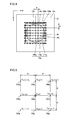
- the above measurement is performed after the substrate is moved in a stepwise fashion (for example in the X direction or the Y direction at a constant pitch P) as shown in Figs. 3 and 4, and thus the position data in the two-dimensional direction (the X direction and the Y direction) and the displacement value data in the Z direction of a measurement point adjacent to arbitrarily specified measurement point 100p at pitch P can be obtained.
- the position data in the two-dimensional direction (the X direction and the Y direction) and the displacement value data in the Z direction of each of the plurality of measurement points 10p on rear surface 10r of the substrate (GaN crystal substrate 10) can be obtained.
- the position data in the two-dimensional direction (the X direction and the Y direction) and the displacement value data in the Z direction obtained as described above are collected to data analysis unit 18.
- the plurality of displacement values respectively corresponding to the plurality of measurement points 10p on rear surface 10r of the substrate (GaN crystal substrate 10) can be detected with measurement points 120a and 120b removed as described below.
- measurement points 120a and 120b can be removed by detecting only arbitrarily specified measurement point 100p which has distance L to laser displacement meter 15 satisfying the relation La ⁇ L ⁇ Lb, where La is a distance between laser displacement meter 15 and surface 12a of the non-concave portion of substrate support table 12, and Lb is a distance between laser displacement meter 15 and surface 12b of the concave portion of substrate support table 12. Consequently, the plurality of displacement values respectively corresponding to the plurality of measurement points 10p on rear surface 10r of the substrate (GaN crystal substrate 10) can be obtained.
- a median filter is a filter replacing a displacement value z (a, b) (meaning a displacement value corresponding to arbitrarily specified measurement point 100p; hereinafter the same applies) specified arbitrarily among the plurality of displacement values (meaning the plurality of displacement values respectively corresponding to the plurality of measurement points 10p on rear surface 10r of the substrate (GaN crystal substrate 10); hereinafter the same applies) by a median obtained when arranging the displacement value z (a, b) and a plurality of displacement values z (a-1, b+1) , z (a-1, b) , z (a-1, b-1) , z (a, b+1) , z (a, b-1), z (a+1, b+1) , z (a+1, b) ,
- the displacement value z (a, b) and the plurality of displacement values z (a-1, b+1) , z (a-1, b) , z (a-1, b-1) , z (a, b+1) , z (a, b-1) , z (a+1, b+1) , z (a+1, b) , and z (a+1, b-1) neighboring the displacement value z (a, b) are arranged in the two-dimensional direction (the X direction and the Y direction) at constant pitch P.
- FIG. 5 shows eight displacement values z (a-1, b+1) , z (a-1, b) , z (a-1, b-1) , z (a, b+1) , z (a, b-1) , z (a+1, b+1) , z (a+1, b) , and z (a+1, b-1) neighboring and surrounding the arbitrarily specified displacement value as the plurality of neighboring displacement values (such a median filter is called an 8-neighborhood median filter), the number of the plurality of neighboring measuring points is not limited to eight. For example, 24 measuring points neighboring a displacement value can also be used (such a median filter is called an 24-neighborhood median filter).
- the outer peripheral portion removal step S3 calculates a plurality of displacement values for calculation by removing from the plurality of displacement values those respectively corresponding to the measurement points in an outer peripheral portion of the substrate.
- the outer peripheral portion removal step S3 it is preferable to remove displacement values respectively corresponding to at least two measurement points 111p and 112p inward from an outer periphery 10e, as the displacement values respectively corresponding to the measurement points in the outer peripheral portion of the substrate (GaN crystal substrate 10), from the plurality of displacement values.
- the smoothing step S4 although there is no limitation on the smoothing step S4 as long as it smoothes the plurality of displacement values for calculation to calculate a warped surface 40, it is preferable to use a Gaussian filter for the step.
- a Gaussian filter is a filter replacing a displacement value z (a, b) specified arbitrarily among the plurality of displacement values for calculation by a weighted average value z' (a, b) of the displacement value z (a, b) and the plurality of displacement values z (a-1, b+1) , z (a-1, b) , z (a-1, b-1) , z (a, b+1) , z (a, b-1) , z (a+1, b+1) , z (a+1, b) , and z (a+1, b-1) neighboring the displacement value z (a, b) , using a Gaussian function f(x, y) as a weighting factor.
- a Gaussian function f(x, y) as a weighting factor.
- a and b are coordinate values of an arbitrarily specified measurement point in the X direction and the Y direction, respectively
- ⁇ is a standard deviation ( ⁇ 2 is a dispersion)
- N is a normalization constant.
- displacement values z (a-1, b+1) , z (a-1, b) , z (a-1, b-1) , z (a, b+1) , z (a, b-1) , z (a+1, b+1) , z (a+1, b) , and z (a+1, b-1) neighboring and surrounding an arbitrarily specified displacement value are used in the above as the plurality of neighboring displacement values (such a Gaussian filter is called an 8-neighborhood Gaussian filter), the number of the plurality of neighboring displacement values is not limited to eight. For example, 24 displacement values neighboring a displacement value can also be used (such a Gaussian filter is called an 24-neighborhood Gaussian filter).
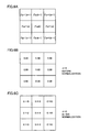
- an 8-neighborhood Gaussian filter specifically means replacing the displacement value z (a, b) specified arbitrarily by the weighted average value z' (a, b) obtained by weighted averaging of the plurality of displacement values z (a-1, b+1) , z (a-1, b) , z (a-1, b-1) , z (a, b+1) , z (a, b) , z (a, b-1) , z (a+1, b+1) , z (a+1, b) , and z (a+1, b-1) shown in Fig.
- the Gaussian function f(x, y) serving as a coefficient of the Gaussian filter is determined by the distance from the measurement point (a, b) of the arbitrarily specified displacement value to the measurement point (x, y) and by standard deviation ⁇ .
- Normalization means correcting coefficients f(x, y) of a Gaussian filter such that a sum of the coefficients f(x, y) is 1, while maintaining ratios between the coefficients f(x, y).
- best fit plane calculation step S5 although there is no particular limitation on the best fit plane calculation step S5 as long as it calculates a best fit plane 50 having the minimum distance to warped surface 40, it is preferable to calculate best fit plane 50 to minimize a sum of squares of every distance between best fit plane 50 and each point represented by each of the plurality of displacement values for calculation subjected to smoothing. With such a least square method, best fit plane 50 representing average inclination of entire rear surface 10r of the substrate (GaN crystal substrate 10) supported at three points can be obtained.
- the warpage calculation step S6 calculates as warpage a sum of a distance D + from best fit plane 50 to a point represented by the greatest displacement value z P of warped surface 40 on one side with respect to best fit plane 50 and a distance D - from best fit plane 50 to a point represented by the greatest displacement value z V of warped surface 40 on the other side with respect to best fit plane 50.
- an optimization cycle C1 including the smoothing step S4, the best fit plane calculation step S5, and the warpage calculation step S6 one or more times it is preferable to repeat an optimization cycle C1 including the smoothing step S4, the best fit plane calculation step S5, and the warpage calculation step S6 one or more times.
- the warped surface of rear surface 10r of substrate 10 can be more smoothed, thereby reducing influence due to surface roughness, and thus the warpage of rear surface 10r can be measured more accurately.
- the number of repeating optimization cycle C1 can be set such that a difference between a value of warpage before an optimization cycle and a value of warpage after the optimization cycle is preferably not more than 0.5 ⁇ m, and more preferably not more than 0.1 ⁇ m. Further, the number can be set such that a ratio of a difference between a value of warpage before an optimization cycle and a value of warpage after the optimization cycle to the value of warpage before the optimization cycle is preferably not more than 0.05, and more preferably not more than 0.01.
- At least one noise removal step S2 is included in an interval between repeated optimization cycles C1, or after the smoothing step S4 in optimization cycle C1.
- the rear surface has a surface roughness Ra (R) satisfying Ra (R) ⁇ 10 ⁇ m.
- Ra also called an arithmetic mean roughness Ra, is a value obtained by sampling a portion having a reference length from a roughness curve in a direction of its mean line, summing up absolute values of deviations from a mean line of the sampled portion to a measurement curve, and calculating an average for the reference length.
- the rear surface has a surface roughness Ra (R) satisfying Ra (R) > 10 ⁇ m, when at least one group-III nitride crystal layer is grown as a semiconductor layer on a side of the crystal growth surface of the GaN crystal substrate, contact between the GaN crystal substrate and the susceptor becomes uneven, which results in uneven distribution of heat transferred from the susceptor to the GaN crystal substrate. From the viewpoint of reducing such uneven distribution of heat in the GaN crystal substrate, it is more preferable that the rear surface has a surface roughness Ra (R) satisfying Ra (R) ⁇ 6 ⁇ m.
- surface roughness Ra (R) of the rear surface if surface roughness Ra (R) of the rear surface is too low, a heat-radiating light beam emitted from the susceptor heated to a high temperature is reflected by the rear surface, and the heat-radiating light beam is less absorbed into the substrate, reducing heating efficiency of the substrate.
- surface roughness Ra (R) of the rear surface preferably satisfies Ra (R) ⁇ 1 ⁇ m, and more preferably satisfies Ra (R) ⁇ 2 ⁇ m.
- the rear surface has a surface roughness Ry (R) satisfying Ra (R) ⁇ 75 ⁇ m.
- Surface roughness Ry also called the maximum height Ry, is a value obtained by sampling a portion having a reference length from a roughness curve in a direction of its mean line, and summing a height from a mean line of the sampled portion to the highest crest and a depth from the mean line of the sampled portion to the lowest valley.
- the rear surface has a surface roughness Ry (R) satisfying Ry (R) > 75 ⁇ m, when at least one group-III nitride crystal layer is grown as a semiconductor layer on the side of the crystal growth surface of the GaN crystal substrate, contact between the GaN crystal substrate and the susceptor becomes uneven, which results in uneven distribution of heat transferred from the susceptor to the GaN crystal substrate. From the viewpoint of reducing such uneven distribution of heat in the GaN crystal substrate, it is more preferable that the rear surface has a surface roughness Ry (R) satisfying Ry (R) ⁇ 50 ⁇ m.
- surface roughness Ry (R) of the rear surface if surface roughness Ry (R) of the rear surface is too low, a heat-radiating light beam emitted from the susceptor heated to a high temperature is reflected by the rear surface, and the heat-radiating light beam is less absorbed into the substrate, reducing heating efficiency of the substrate.
- surface roughness Ry (R) of the rear surface preferably satisfies Ry (R) ⁇ 3 ⁇ m, and more preferably satisfies Ry (R) ⁇ 10 ⁇ m.
- warpage w (C) of the crystal growth surface of the substrate preferably satisfies -50 ⁇ m ⁇ w (C) ⁇ 50 ⁇ m, and more preferably satisfies -35 ⁇ m ⁇ w (C) ⁇ 40 ⁇ m.
- surface roughness Ra (C) of the crystal growth surface preferably satisfies Ra (C) ⁇ 10 nm, and more preferably satisfies Ra (C) ⁇ 5 nm.
- surface roughness Ry (C) of the crystal growth surface preferably satisfies Ry (C) ⁇ 60 nm, and more preferably satisfies Ry (C) ⁇ 30 nm.
- warpage w (C) is defined as a difference in height between a displacement value z CP at the most convex portion and a displacement value z CV at the most concave portion of crystal growth surface 10c.
- the GaN crystal substrate in the present embodiment has a higher absorption coefficient for the heat-radiating light beam in order to improve the heating efficiency of the substrate.
- the GaN crystal substrate in the present embodiment preferably has an absorption coefficient for a light beam having a peak wavelength of 450 nm to 550 nm of not less than 1.5 cm -1 and not more than 10 cm -1 . If the absorption coefficient for such a light beam is lower than 1.5 cm -1 , the light beam passes through the substrate and is not absorbed, and thus the heating efficiency of the substrate is reduced. If the absorption coefficient for such a light beam is higher than 10 cm -1 , the substrate includes many impurities and thus has a low crystallinity.
- the GaN crystal substrate in the present embodiment preferably has a heat conductivity of not less than 160 W/mK in order to reduce heat distribution in the substrate. Furthermore, the GaN crystal substrate in the present embodiment preferably has a heat expansion coefficient of not less than 3 ⁇ 10 -6 K -1 and not more than 6 ⁇ 10 -6 K -1 in order to suppress deformation of the substrate when a temperature is increased or decreased.
- a method of manufacturing a GaN crystal substrate in accordance with the present invention is a method of manufacturing the GaN crystal substrate in the first embodiment, including the steps of cutting GaN crystal substrate 10 out of a GaN crystal 1 (see Fig. 8(a)) and processing rear surface 10r of GaN crystal substrate 10 (see Fig. 8(b)), and the step of processing rear surface 10r of GaN crystal substrate 10 includes at least one of the steps of grinding rear surface 10r, lapping rear surface 10r, and etching rear surface 10r.
- the step of cutting GaN crystal substrate 10 out of GaN crystal 1 is the step of cutting GaN crystal substrate 10 of a predetermined shape out of grown GaN crystal 1 using an inner diameter blade, an outer diameter blade, a wire saw, or the like.
- vapor phase epitaxy such as HVPE or MOVPE is preferably used because a large-sized crystal having a diameter of not less than 5.08 cm (2 inches) is obtained relatively in a short period or time.
- the step of processing rear surface 10r of GaN crystal substrate 10 includes at least one of the step of grinding rear surface 10r of GaN crystal substrate 10 (the grinding step), the step of lapping rear surface 10r of GaN crystal substrate 10 (the lapping step), and etching rear surface 10r of GaN crystal substrate 10 (the etching step).
- the step of processing the rear surface of the GaN crystal substrate including the steps described above, a GaN crystal substrate in which a rear surface opposite to a crystal growth surface has a warpage w (R) satisfying -50 ⁇ m ⁇ w (R) ⁇ 50 ⁇ m can be obtained.
- a GaN crystal substrate having a rear surface with a surface roughness Ra (R) satisfying Ra (R) ⁇ 10 ⁇ m and/or a surface roughness Ry (R) satisfying Ry (R) ⁇ 75 ⁇ m can be obtained.
- grinding is to rotate fixed abrasive grains made by fixing abrasive grains with a bond at a high speed, bring the fixed abrasive grains into contact with an object, and scrape off a surface of the object.
- Such grinding provides a rough surface.
- fixed abrasive grains including abrasive grains formed of SiC, Al 2 O 3 , diamond, CBN (cubic boron nitride; hereinafter the same applies) or the like having a hardness higher than that of the GaN crystal, and having a grain size of about not less than 10 ⁇ m and not more than 100 ⁇ m are preferably used.
- lapping is to bring a rotating surface plate and a rotating object into contact with each other with free abrasive grains (meaning abrasive grains which are not fixed; hereinafter the same applies) interposed therebetween or bring rotating fixed abrasive grains and a rotating object into contact with each other, and rub a surface of the object.
- free abrasive grains meaning abrasive grains which are not fixed; hereinafter the same applies
- Such lapping provides a surface having a surface roughness lower than that obtained by grinding and higher than that obtained by polishing.
- abrasive grains formed of SiC, Al 2 O 3 , diamond, CBN or the like having a hardness higher than that of the GaN crystal, and having a grain size of about not less than 0.5 ⁇ m and not more than 15 ⁇ m are preferably used.
- etching is to chemically or physically erode a surface of an object to remove an affected layer and residues left after the steps of cutting the object and subsequently grinding and/or lapping a surface of the object (such as shavings left after cutting, grinding and lapping, abrasive grains, and a wax) (10u: an etched portion). Also by such etching, surface roughness is maintained.
- wet etching using an etching agent is preferably performed.
- Examples of a preferable etching agent include a mixed solution of NH 3 and H 2 O 2 , a KOH solution, a NaOH solution, an HCl solution, an H 2 SO 4 solution, an H 3 PO 4 solution, a mixed solution of H 3 PO 4 and H 2 SO 4 , and the like.
- Water is used as a preferable solvent for the solutions and the mixed solutions described above.
- the etching agent can also be diluted with a solvent such as water as appropriate for use.
- the step of processing the crystal growth surface of the GaN crystal substrate is performed.
- the crystal growth surface of the GaN crystal substrate has warpage w (C) satisfying -50 ⁇ m ⁇ w (C) ⁇ 50 ⁇ m, surface roughness Ra (C) satisfying Ra (C) ⁇ 10 nm, and surface roughness Ry (C) satisfying Ry (C) ⁇ 60 nm.
- a polishing step is performed in the step of processing the crystal growth surface of the GaN crystal substrate cut out of the GaN crystal, in addition to a grinding step, a lapping step, and/or an etching step similar to the grinding step, the lapping step, and/or the etching step in the step of processing the rear surface.
- Polishing is to bring a rotating polishing pad and a rotating object into contact with each other with free abrasive grains interposed therebetween or bring rotating fixed abrasive grains and a rotating object into contact with each other, and finely rub and smooth a surface of the object.
- Such polishing provides a crystal growth surface having a surface roughness lower than that obtained by lapping.
- CMP chemical mechanical polishing
- Mechanical polishing or CMP is a technique bringing a rotating polishing pad and a rotating object into contact with each other, with a slurry containing abrasive grains interposed therebetween, to mechanically or chemically and mechanically polish a surface of the object.
- the slurry is acidic having pH ⁇ 5 or basic having PH ⁇ 9, or is added with an oxidizer such as hydrogen peroxide (H 2 O 2 ), dichloroisocyanurate, nitric acid, potassium permanganate, or copper chloride and thus has an improved ORP (oxidation-reduction potential) (for example, ORP ⁇ 400 mV), in order to improve a chemical polishing effect.
- an oxidizer such as hydrogen peroxide (H 2 O 2 ), dichloroisocyanurate, nitric acid, potassium permanganate, or copper chloride
- ORP oxidation-reduction potential
- an embodiment of a method of manufacturing a semiconductor device in accordance with the present invention includes the step of preparing GaN crystal substrate 10 in the first embodiment as a substrate and growing at least one group-III nitride crystal layer 20 on the side of crystal growth surface 10c of GaN crystal substrate 10.
- group-III nitride crystal layer 20 can be formed evenly and stably as a semiconductor layer on the side of crystal growth surface 10c of GaN crystal substrate 10, and thus a semiconductor device 99 having excellent properties can be obtained.
- an n-type GaN layer 21, an In 0.2 Ga 0.8 N layer 22, an Al 0.2 Ga 0.8 N layer 23, and a p-type GaN layer 24 are formed in order as group-III nitride crystal layer 20 on crystal growth surface 10c of GaN crystal substrate 10 to obtain a wafer 80 including stacked semiconductor layers (hereinafter referred to as a semiconductor-layer-stacked wafer 80).
- a wafer 80 including stacked semiconductor layers hereinafter referred to as a semiconductor-layer-stacked wafer 80.
- an n-side electrode 81 is formed on rear surface 10r of GaN crystal substrate 10 of semiconductor-layer-stacked wafer 80, and a p-side electrode 82 is formed on an upper surface of group-III nitride crystal layer 20 (that is, an upper surface of p-type GaN layer 24) to obtain a semiconductor device wafer 90.
- semiconductor device wafer 90 is divided into chips to obtain an LED (light emitting diode) as semiconductor device 99.
- GaN crystal substrate 10 measuring 5.08 cm (2 inches) in diameter by 550 ⁇ m in thickness was cut out of GaN crystal 1 grown by HVPE.
- rear surface 10r and crystal growth surface 10c of GaN crystal substrate 10 were processed as described below.
- the rear surface was subjected to grinding using fixed abrasive grains made by fixing CBN abrasive grains having a grain size of 125 ⁇ m with a bond (the grinding step), lapping using diamond abrasive grains having a grain size of 24 ⁇ m (the lapping step), and etching using a mixed aqueous solution of NH 3 and H 2 O 2 in which 30% by mass ammonia water, 40% by mass hydrogen peroxide water, and pure water were mixed in the volume ratio of 1:1:2 (the etching step).
- warpage w (R) of rear surface 10r of GaN crystal substrate 10 subjected to the above processing was measured as described below, using a laser displacement meter employing the laser focus technique (LT-9010 (laser output unit) and LT-9500 (laser control unit) manufactured by Keyence Corporation), an XY position controller (CP-500 manufactured by COMS Co., Ltd.), and a high-speed analog voltage data collection apparatus (CA-800 manufactured by COMS Co., Ltd.).
- a red color semiconductor laser having a laser wavelength of 670 nm was used for the laser displacement meter.
- GaN crystal substrate 10 was disposed on substrate support table 12 such that the outer peripheral portion of crystal growth surface 10c thereof was supported by three supporting portions 12h. Then, laser displacement meter 15 was used to detect a plurality of displacement values respectively corresponding to the plurality of measurement points 10p on rear surface 10r of GaN crystal substrate 10 (the substrate detection step S1). On this occasion, measurement points 10p were arranged with pitch P of 700 ⁇ m, and a plurality of displacement values respectively corresponding to about 5000 measurement points 10p was measured. Next, noise contained in the plurality of displacement values was removed using an 8-neighborhood median filter (the noise removal step S2). Thereafter, a plurality of displacement values for calculation was calculated by removing from the plurality of displacement values those respectively corresponding to up to three measurement points inward from outer periphery 10e of GaN crystal substrate 10 (the outer peripheral portion removal step S3).
- a best fit plane was calculated to minimize the sum of squares of every distance between best fit plane 50 and each point represented by each of the plurality of displacement values for calculation subjected to smoothing (the best fit plane calculation step S5).
- the warpage calculation step S6 the sum of a distance from the best fit plane to a point represented by the greatest displacement value of the warped surface on one side with respect to the best fit plane and a distance from the best fit plane to a point represented by the greatest displacement value of the warped surface on the other side with respect to the best fit plane was calculated as warpage (the warpage calculation step S6).
- the warpage calculated as described above was 57.4 ⁇ m.
- warpage w (R) of the rear surface of the GaN crystal substrate was calculated at 54.5 ⁇ m. Further, when warpage w (C) of crystal growth surface 10c of GaN crystal substrate 10 subjected to the above processing was measured using a flatness tester employing optical interferometry, warpage w (C) was 48.2 ⁇ m.
- surface roughness Ra (R) of rear surface 10r and surface roughness Ra (C) of crystal growth surface 10c of GaN crystal substrate 10 subjected to the above processing were calculated by: performing measurement in a range of 110 ⁇ m x 80 ⁇ m using a 3D-SEM (three-dimensional scanning electron microscope) and in a range of 750 ⁇ m x 700 ⁇ m using the laser displacement meter employing the laser focus technique, respectively; sampling a portion having a reference length from a roughness curve arbitrarily specified in each measurement range, in a direction of a mean line of the roughness curve; summing up absolute values of deviations from a mean line of the sampled portion to a measurement curve; and calculating an average for the reference length.
- surface roughness Ry (R) of rear surface 10r and surface roughness Ry (C) of crystal growth surface 10c of GaN crystal substrate 10 subjected to the above processing were calculated by: performing measurement in a range of 750 ⁇ m x 700 ⁇ m using the laser displacement meter employing the laser focus technique; sampling a portion having a reference length from a roughness curve arbitrarily specified in each measurement range, in a direction of a mean line of the roughness curve; and summing a height from a mean plane of the sampled portion to the highest crest and a depth from the mean plane of the sampled portion to the lowest valley.
- an absorption coefficient of GaN crystal substrate 10 subjected to the above processing for a light beam having a peak wavelength of 450 nm to 550 nm was measured using a spectrometer, and it was found that GaN crystal substrate 10 had an absorption coefficient of 6.8 cm -1 .
- heat conductivity of GaN crystal substrate 10 was measured in a range of 18 mm ⁇ 18 mm by two-dimensional measurement using laser flash, and it was found that GaN crystal substrate 10 had a heat conductivity of 165 W/mK.
- a heat expansion coefficient of GaN crystal substrate 10 was measured by laser interferometry, and it was found that GaN crystal substrate 10 had a heat expansion coefficient of 4.2 ⁇ 10 -6 K -1 .
- n-type GaN layer 21, 3 nm thick In 0.2 Ga 0.8 N layer 22, 60 nm thick Al 0.2 Ga 0.8 N layer 23, and 150 nm thick p-type GaN layer 24 were grown in order as group-III nitride crystal layer 20 on crystal growth surface 10c of GaN crystal substrate 10 by means of MOVPE, to obtain semiconductor-layer-stacked wafer 80.
- Light emission intensity distribution in the obtained semiconductor-layer-stacked wafer 80 was evaluated by photoluminescence (hereinafter referred to as PL).
- a laser beam having an energy greater than that of a bandgap of any layer in group-III nitride crystal layer 20 (a He-Cd laser beam having a peak wavelength of 325 nm) was applied to a plurality of measurement points on a main surface on the side of group-III nitride crystal layer 20 of semiconductor-layer-stacked wafer 80 having a diameter of 5.08 cm (2 inches), and intensity of excited light emission was measured.
- the measurement points were disposed all over the main surface on the side of group-III nitride crystal layer 20 of semiconductor-layer-stacked wafer 80, and arranged with a pitch of 1 mm in the two-dimensional direction parallel to the main surface.
- Light emission intensity distribution in semiconductor-layer-stacked wafer 80 was evaluated using a percentage of a light emission intensity I E in an outer peripheral portion ranging from an outer periphery 80e to 5 mm inward therefrom having the smallest light emission intensity to a light emission intensity I C in a central portion having the greatest light emission intensity (100 ⁇ I E /I C , hereinafter referred to as a relative light emission intensity in the outer peripheral portion).
- the relative light emission intensity in the outer peripheral portion in the present comparative example was 0.06, meaning that the light emission intensity distribution was large. Table 1 shows the result.
- n-side electrode 81 measuring 80 ⁇ m in diameter by 100 nm in thickness was formed on rear surface 10r of GaN crystal substrate 10 at a position to be a central portion of a chip when semiconductor-layer-stacked wafer 80 was cut into chips, and 100 nm thick p-side electrode 82 was formed on the upper surface of p-type GaN layer 24. Thereby, semiconductor device wafer 90 was obtained.
- semiconductor device wafer 90 was divided into chips each measuring 400 ⁇ m by 400 ⁇ m, and thus an LED serving as semiconductor device 99 was obtained.
- Obtained semiconductor device 99 had a yield (meaning a percentage of the number of semiconductor devices having a predetermined light emission intensity and obtained as products to the total number of semiconductor devices produced as chips; hereinafter the same applies) of as low as 25%. Table 1 shows the result.
- a GaN crystal substrate was manufactured as in the first comparative example except that, during manufacturing the GaN crystal substrate, a rear surface thereof was subjected to grinding using fixed abrasive grains made by fixing CBN abrasive grains having a grain size of 84 ⁇ m with a bond (the grinding step), lapping using SiC abrasive grains having a grain size of 12 ⁇ m (the lapping step), and etching using a mixed aqueous solution of H 3 PO 4 and H 2 SO 4 in which an 85% by mass phosphoric acid aqueous solution and a 90% by mass sulfuric acid aqueous solution were mixed in the volume ratio of 1:1 (the etching step).
- the rear surface of the obtained GaN crystal substrate had a warpage w (R) of -22.8 ⁇ m, a surface roughness Ra (R) of 10.2 ⁇ m, and a surface roughness Ry (R) of 78.5 ⁇ m.
- the crystal growth surface of the GaN crystal substrate had a warpage w (C) of -17.4 ⁇ m, and had surface roughnesses Ra (C) and Ry (C) similar to those in the first comparative example.
- the GaN crystal substrate had an absorption coefficient for a light beam having a peak wavelength of 450 nm to 550 nm, a heat conductivity, and a heat expansion coefficient similar to those in the first comparative example.
- the GaN crystal substrate obtained in the present example was used to prepare a semiconductor-layer-stacked wafer and then a semiconductor device wafer, and finally manufacture a semiconductor device, as in the first comparative example.
- the semiconductor-layer-stacked wafer of the present example had a high relative light emission intensity in the outer peripheral portion of 0.16 (meaning that the light emission intensity distribution was small). Further, the semiconductor device had a high yield of 44%. Table 1 shows the result.
- a GaN crystal substrate was manufactured as in the first comparative example except that, during manufacturing the GaN crystal substrate, a rear surface thereof was subjected to grinding using fixed abrasive grains made by fixing Al 2 O 3 abrasive grains having a grain size of 63 ⁇ m with a bond (the grinding step), lapping using Al 2 O 3 abrasive grains having a grain size of 8 ⁇ m (the lapping step), and etching using a 25% by mass KOH aqueous solution (the etching step). Then, warpages and surface roughnesses of the rear surface and the crystal growth surface of the GaN crystal substrate were measured.
- the rear surface of the obtained GaN crystal substrate had a warpage w (R) of -19.1 ⁇ m, a surface roughness Ra (R) of 6.8 ⁇ m, and a surface roughness Ry (R) of 55 ⁇ m.
- the crystal growth surface of the GaN crystal substrate had a warpage w (C) of -16.7 ⁇ m, and had surface roughnesses Ra (C) and Ry (C) similar to those in the first comparative example.
- the GaN crystal substrate had an absorption coefficient for a light beam having a peak wavelength of 450 nm to 550 nm, a heat conductivity, and a heat expansion coefficient similar to those in the first comparative example.
- the GaN crystal substrate obtained in the present example was used to prepare a semiconductor-layer-stacked wafer and then a semiconductor device wafer, and finally manufacture a semiconductor device, as in the first comparative example.
- the semiconductor-layer-stacked wafer of the present example had a high relative light emission intensity in the outer peripheral portion of 0.29 (meaning that the light emission intensity distribution was small). Further, the semiconductor device had a high yield of 57%. Table 1 shows the result.
- a GaN crystal substrate was manufactured as in the first comparative example except that, during manufacturing the GaN crystal substrate, a rear surface thereof was subjected to grinding using fixed abrasive grains made by fixing diamond abrasive grains having a grain size of 32 ⁇ m with a bond (the grinding step), and etching using a 25% by mass KOH aqueous solution (the etching step). Then, warpages and surface roughnesses of the rear surface and the crystal growth surface of the GaN crystal substrate were measured.
- the rear surface of the obtained GaN crystal substrate had a warpage w (R) of -3.4 ⁇ m, a surface roughness Ra (R) of 4.9 ⁇ m, and a surface roughness Ry (R) of 31.9 ⁇ m.
- the crystal growth surface of the GaN crystal substrate had a warpage w (C) of -4.6 ⁇ m, and had surface roughnesses Ra (C) and Ry (C) similar to those in the first comparative example.
- the GaN crystal substrate had an absorption coefficient for a light beam having a peak wavelength of 450 nm to 550 nm, a heat conductivity, and a heat expansion coefficient similar to those in the first comparative example.
- the GaN crystal substrate obtained in the present example was used to prepare a semiconductor-layer-stacked wafer and then a semiconductor device wafer, and finally manufacture a semiconductor device, as in the first comparative example.
- the semiconductor-layer-stacked wafer of the present example had a high relative light emission intensity in the outer peripheral portion of 0.41 (meaning that the light emission intensity distribution was small). Further, the semiconductor device had a high yield of 70%. Table 1 shows the result.
- a GaN crystal substrate was manufactured as in the first comparative example except that, during manufacturing the GaN crystal substrate, a rear surface thereof was subjected to grinding using fixed abrasive grains made by fixing SiC abrasive grains having a grain size of 30 ⁇ m with a bond (the grinding step), lapping using diamond abrasive grains having a grain size of 6 ⁇ m (the lapping step), and etching using a mixed aqueous solution of NH 3 and H 2 O 2 in which 30% by mass ammonia water, 40% by mass hydrogen peroxide water, and pure water were mixed in the volume ratio of 1:1:6 (the etching step). Then, warpages and surface roughnesses of the rear surface and the crystal growth surface of the GaN crystal substrate were measured.
- the rear surface of the obtained GaN crystal substrate had a warpage w (R) of 4.8 ⁇ m, a surface roughness Ra (R) of 3.8 ⁇ m, and a surface roughness Ry (R) of 23.8 ⁇ m.
- the crystal growth surface of the GaN crystal substrate had a warpage w (C) of 2.8 ⁇ m, and had surface roughnesses Ra (C) and Ry (C) similar to those in the first comparative example.
- the GaN crystal substrate had an absorption coefficient for a light beam having a peak wavelength of 450 nm to 550 nm, a heat conductivity, and a heat expansion coefficient similar to those in the first comparative example.
- the GaN crystal substrate obtained in the present example was used to prepare a semiconductor-layer-stacked wafer and then a semiconductor device wafer, and finally manufacture a semiconductor device, as in the first comparative example.
- the semiconductor-layer-stacked wafer of the present example had a high relative light emission intensity in the outer peripheral portion of 0.38 (meaning that the light emission intensity distribution was small). Further, the semiconductor device had a high yield of 68%. Table 1 shows the result.
- a GaN crystal substrate was manufactured as in the first comparative example except that, during manufacturing the GaN crystal substrate, a rear surface thereof was subjected to grinding using fixed abrasive grains made by fixing SiC abrasive grains having a grain size of 37 ⁇ m with a bond (the grinding step), and etching using a 25% by mass KOH aqueous solution (the etching step). Then, warpages and surface roughnesses of the rear surface and the crystal growth surface of the GaN crystal substrate were measured.
- the rear surface of the obtained GaN crystal substrate had a warpage w (R) of 9.9 ⁇ m, a surface roughness Ra (R) of 5.5 ⁇ m, and a surface roughness Ry (R) of 38.7 ⁇ m.
- the crystal growth surface of the GaN crystal substrate had a warpage w (C) of 10.4 ⁇ m, and had surface roughnesses Ra (C) and Ry (C) similar to those in the first comparative example.
- the GaN crystal substrate had an absorption coefficient for a light beam having a peak wavelength of 450 nm to 550 nm, a heat conductivity, and a heat expansion coefficient similar to those in the first comparative example.
- the GaN crystal substrate obtained in the present example was used to prepare a semiconductor-layer-stacked wafer and then a semiconductor device wafer, and finally manufacture a semiconductor device, as in the first comparative example.
- the semiconductor-layer-stacked wafer of the present example had a high relative light emission intensity in the outer peripheral portion of 0.30 (meaning that the light emission intensity distribution was small). Further, the semiconductor device had a high yield of 65%. Table 1 shows the result.
- a GaN crystal substrate was manufactured as in the first comparative example except that, during manufacturing the GaN crystal substrate, a rear surface thereof was subjected to grinding using fixed abrasive grains made by fixing diamond abrasive grains having a grain size of 74 ⁇ m with a bond (the grinding step), lapping using CBN abrasive grains having a grain size of 15 ⁇ m (the lapping step), and etching using an 85% by mass H 3 PO 4 aqueous solution (the etching step). Then, warpages and surface roughnesses of the rear surface and the crystal growth surface of the GaN crystal substrate were measured.
- the rear surface of the obtained GaN crystal substrate had a warpage w (R) of 19.3 ⁇ m, a surface roughness Ra (R) of 10.8 ⁇ m, and a surface roughness Ry (R) of 81.9 ⁇ m.
- the crystal growth surface of the GaN crystal substrate had a warpage w (C) of 23.0 ⁇ m, and had surface roughnesses Ra (C) and Ry (C) similar to those in the first comparative example.
- the GaN crystal substrate had an absorption coefficient for a light beam having a peak wavelength of 450 nm to 550 nm, a heat conductivity, and a heat expansion coefficient similar to those in the first comparative example.
- the GaN crystal substrate obtained in the present example was used to prepare a semiconductor-layer-stacked wafer and then a semiconductor device wafer, and finally manufacture a semiconductor device, as in the first comparative example.
- the semiconductor-layer-stacked wafer of the present example had a high relative light emission intensity in the outer peripheral portion of 0.26 (meaning that the light emission intensity distribution was small). Further, semiconductor device had a high yield of 61%. Table 1 shows the result.
- a semiconductor-layer-stacked wafer having smaller light emission intensity distribution is obtained and the yield of a semiconductor device is further increased by forming at least one group-III nitride crystal layer on the side of a crystal growth surface of a GaN crystal substrate in which a rear surface opposite to the crystal growth surface has a warpage (R) satisfying -50 ⁇ m ⁇ w (R) ⁇ 50 ⁇ m, a surface roughness Ra (R) satisfying Ra (R) ⁇ 10 ⁇ m, and a surface roughness Ry (R) satisfying Ry (R) ⁇ 75 ⁇ m.
- Fig. 10 shows relation between the warpage of the rear surface of the GaN crystal substrate and the yield of the semiconductor device in a plurality of semiconductor devices obtained in the third embodiment.
- Fig. 10 includes points concerning the first comparative example and the first to sixth examples.
- the yield of the semiconductor device was increased when warpage (R) of the rear surface of the GaN crystal substrate was -50 ⁇ m ⁇ w (R) ⁇ 50 ⁇ m, and further increased when warpage (R) was -35 ⁇ m ⁇ w (R) ⁇ 45 ⁇ m.
- a preferable range of the warpage of the rear surface is larger on a positive (+) side than on a negative (-) side because, as has been already contemplated referring to Figs.
Landscapes
- Chemical & Material Sciences (AREA)
- Metallurgy (AREA)
- Engineering & Computer Science (AREA)
- Crystallography & Structural Chemistry (AREA)
- Materials Engineering (AREA)
- Organic Chemistry (AREA)
- General Chemical & Material Sciences (AREA)
- Chemical Kinetics & Catalysis (AREA)
- Inorganic Chemistry (AREA)
- Physics & Mathematics (AREA)
- General Physics & Mathematics (AREA)
- Crystals, And After-Treatments Of Crystals (AREA)
- Weting (AREA)
- Led Devices (AREA)
Abstract
Description
- The present invention relates to a GaN crystal substrate used in a semiconductor device such as a light emitting element, an electronic element, or a semiconductor sensor, a method of manufacturing the same, and a method of manufacturing a semiconductor device for which the GaN crystal substrate is selected as a substrate.
- A GaN crystal substrate is very useful as a substrate for a semiconductor device such as a light emitting element, an electronic element, or a semiconductor sensor. Such a GaN crystal substrate is formed by cutting a GaN crystal grown by vapor phase epitaxy such as HVPE (hydride vapor phase epitaxy) or MOVPE (metalorganic vapor phase epitaxy) into substrates of a predetermined shape, and grinding, lapping, and/or etching a main surface thereof.
- In order to obtain a semiconductor device having excellent properties by forming at least one semiconductor layer having good crystallinity (meaning orderliness of atomic arrangement in a crystal; hereinafter the same applies) on a crystal growth surface, which is one main surface, of a GaN crystal substrate, there has been proposed a GaN crystal substrate having reduced warpage and surface roughness on a crystal growth surface (see for example
Japanese Patent Laying-Open No. 2000-012900 - Even when the crystal growth surface of a GaN crystal substrate has reduced warpage and surface roughness, however, if a rear surface (meaning the other main surface, that is, a surface opposite to the crystal growth surface; hereinafter the same applies) of the GaN crystal substrate has a large warpage, this causes an increase in a gap portion formed between the rear surface of the substrate and a susceptor (meaning a table on which a substrate is disposed; hereinafter the same applies) when a semiconductor layer is formed on the crystal growth surface of the substrate. As a result, heat transferred from the susceptor to the substrate is unevenly distributed, and the semiconductor layer cannot be formed evenly and stably on the crystal growth surface of the substrate. Consequently, there has been a problem that a semiconductor layer having good crystallinity cannot be formed on the crystal growth surface of the substrate, and thus a semiconductor device having excellent properties cannot be obtained. Further, although the rear surface of a GaN crystal substrate generally has a surface roughness greater than a surface roughness of the crystal growth surface, the same problem as described above has occurred when the rear surface has an extremely greater surface roughness.
- One object of the present invention is to provide a GaN crystal substrate having a rear surface with a reduced warpage and allowing a semiconductor layer having good crystallinity to be formed on a crystal growth surface thereof, a method of manufacturing the same, and a method of manufacturing a semiconductor device.
- The present invention is a GaN crystal substrate having a crystal growth surface and a rear surface opposite to the crystal growth surface, the rear surface having a warpage w(R) satisfying -50 µm ≤ w(R) ≤ 50 µm.
- In the GaN crystal substrate in accordance with the present invention, the rear surface can have a surface roughness Ra(R) satisfying Ra(R) ≤ 10 µm. Further, the rear surface can have a surface roughness Ry(R) satisfying Ry(R) ≤ 75 µm. Furthermore, the crystal growth surface can have a warpage w(C) satisfying -50 µm ≤ w(C) ≤ 50 µm, a surface roughness Ra(C) satisfying Ra(C) ≤ 10 nm, and a surface roughness Ry(C) satisfying Ry(C) ≤ 60 nm.
- Further, the present invention is a method of manufacturing the GaN crystal substrate described above, including the steps of cutting the GaN crystal substrate out of a grown GaN crystal, and processing the rear surface of the GaN crystal substrate, wherein the step of processing the rear surface of the GaN crystal substrate includes at least one of the steps of grinding the rear surface, lapping the rear surface, and etching the rear surface.
- Furthermore, the present invention is a method of manufacturing a semiconductor device, including the step of preparing the GaN crystal substrate described above as a substrate, and growing at least one group-III nitride crystal layer on a side of the crystal growth surface of the GaN crystal substrate.
- According to the present invention, a GaN crystal substrate having a rear surface with a reduced warpage and allowing a semiconductor layer having good crystallinity to be formed on a crystal growth surface thereof, a method of manufacturing the same, and a method of manufacturing a semiconductor device can be provided.
- The foregoing and other objects, features, aspects and advantages of the present invention will become more apparent from the following detailed description of the present invention when taken in conjunction with the accompanying drawings.
-
- Figs. 1A and 1B are schematic cross sectional views showing warpage of a rear surface of a GaN crystal substrate in accordance with the present invention.
- Fig. 2 is a flow chart illustrating a method of measuring the warpage of the rear surface of the GaN crystal substrate in accordance with the present invention.
- Fig. 3 is a schematic view of a measuring apparatus used in the method of measuring the warpage of the rear surface of the GaN crystal substrate in accordance with the present invention.
- Fig. 4 is a schematic plan view showing a plurality of measurement points in the method of measuring the warpage of the rear surface of the GaN crystal substrate in accordance with the present invention.
- Fig. 5 is a schematic view showing an arrangement of the plurality of measurement points.
- Fig. 6A is a schematic view of a kernel for an 8-neighborhood Gaussian filter illustrating positions at which Gaussian functions f(x, y) serving as coefficients are arranged.
- Fig. 6B is a schematic view of a kernel for an 8-neighborhood Gaussian filter illustrating an arrangement of coefficients with σ=5 before normalization.
- Fig. 6C is a schematic view of a kernel for an 8-neighborhood Gaussian filter illustrating an arrangement of coefficients with σ=5 after normalization.
- Figs. 7A and 7B are schematic views showing a warpage calculation step in the method of measuring the warpage of the rear surface of the GaN crystal substrate in accordance with the present invention.
- Fig. 8 is a schematic cross sectional view showing a method of manufacturing the GaN crystal substrate in accordance with the present invention.
- Fig. 9 is a schematic cross sectional view showing a method of manufacturing a semiconductor device in accordance with the present invention.
- Fig. 10 is a view showing relation between the warpage of the rear surface of the GaN crystal substrate and a yield of the semiconductor device.
- Referring to Figs. 1A and 1B, in an embodiment of a GaN crystal substrate in accordance with the present invention, a
rear surface 10r opposite to acrystal growth surface 10c has a warpage w(R) satisfying -50 µm ≤ w(R) ≤ 50 µm, where a warpage causingrear surface 10r to be concavely curved as shown in Fig. 1A is indicated with a positive (+) sign, and a warpage causingrear surface 10r to be convexly curved as shown in Fig. 1B is indicated with a negative (-) sign. Warpage w(R) is defined as a difference in height between a displacement value zP at the most convex portion and a displacement value zv at the most concave portion ofrear surface 10r. - Referring to Figs. 1A and 1B, if warpage w(R) of
rear surface 10r satisfies w(R) < -50 µm or w(R) > 50 µm, agap portion 9s formed between aGaN crystal substrate 10 and asusceptor 9 is increased. This results in uneven distribution of heat transferred fromsusceptor 9 toGaN crystal substrate 10 when at least one group-IIInitride crystal layer 20 is grown as a semiconductor layer oncrystal growth surface 10c ofGaN crystal substrate 10. As a result,semiconductor layer 20 cannot be grown evenly and stably, which makes it difficult to manufacture a semiconductor device formed evenly and having excellent properties. - In view of the above, it is more preferable that
rear surface 10r has warpage w(R) satisfying -35 µm ≤ w(R) ≤ 45 µm. When the warpage ofrear surface 10r is indicated with a positive (+) sign,gap portion 9s formed betweenrear surface 10r and a surface ofsusceptor 9 is a closed space as shown in Fig. 1A. On the other hand, when the warpage ofrear surface 10r is indicated with a negative (-) sign,gap portion 9s formed betweenrear surface 10r and the surface ofsusceptor 9 is an open space as shown in Fig. 1B. Therefore, whensemiconductor layer 20 is formed oncrystal growth surface 10c ofsubstrate 10, heat distribution in the substrate when the warpage is indicated with a positive (+) sign is smaller than heat distribution in the substrate when the warpage indicated with a negative (-) sign. It is contemplated that a preferable range of the warpage is larger on a positive (+) side than on a negative (-) side. - Since
rear surface 10r of the substrate (GaN crystal substrate 10) generally has a high surface roughness, the warpage ofrear surface 10r of the substrate (GaN crystal substrate 10) was measured by a method for accurately measuring the warpage ofrear surface 10r described below. Referring to Fig. 2, the measurement method is a method of measuring warpage of a rear surface opposite to a crystal growth surface of a substrate using a laser displacement meter, and the substrate is disposed on a substrate support table. The method includes: a substratedetection step S 1 detecting a plurality of displacement values respectively corresponding to a plurality of measurement points on the rear surface of the substrate using the laser displacement meter; a noise removal step S2 removing noise contained in the plurality of displacement values; an outer peripheral portion removal step S3 calculating a plurality of displacement values for calculation by removing from the plurality of displacement values those respectively corresponding to the measurement points in an outer peripheral portion of the substrate; a smoothing step S4 smoothing the plurality of displacement values for calculation to calculate a warped surface; a best fit plane calculation step S5 calculating a best fit plane having the minimum distance to the warped surface; and a warpage calculation step S6 calculating as warpage a sum of a distance from the best fit plane to a point represented by the greatest displacement value of the warped surface on one side with respect to the best fit plane and a distance from the best fit plane to a point represented by the greatest displacement value of the warped surface on the other side with respect to the best fit plane. With the measurement method described above, even for a substrate having a rear surface with a high surface roughness (for example, with a surface roughness Ra of not less than 50 nm), the warpage of the rear surface of the substrate can be measured. It is to be noted that surface roughness Ra is a value obtained by sampling a portion having a reference length from a roughness curve in a direction of its mean line, summing up absolute values of deviations from a mean line of the sampled portion to a measurement curve, and calculating an average for the reference length. Further, in Fig. 2, the step surrounded with a solid frame is an indispensable step, and the step surrounded with a dashed frame is an arbitrary step. - Turning to Fig. 3, a
laser displacement meter 15 is an apparatus measuring a displacement ofrear surface 10r of the substrate (GaN crystal substrate 10) by applying alaser beam 31 onrear surface 10r of the substrate (GaN crystal substrate 10). There is no particular limitation on the type of the laser, and for example a red color semiconductor laser having a wavelength of 670 nm is used. There is no particular limitation on the measuring technique, and for example a laser focus technique is used. Although a laser displacement meter employing the laser focus technique has a lower accuracy than a flatness tester employing optical interferometry, it can measure a rough rear surface with surface roughness Ra of not less than 50 nm. Further, unlike the flatness tester employing optical interferometry, the laser displacement meter employing the laser focus technique can obtain a reflectedbeam 31r, and thus it can analyze and process a displacement value. - Referring to Figs. 3 and 4, the substrate (GaN crystal substrate 10) is disposed on a substrate support table 12. Although there is no particular limitation on how to dispose the substrate (GaN crystal substrate 10) on substrate support table 12, the substrate (GaN crystal substrate 10) is preferably disposed on substrate support table 12 having three supporting
portions 12h such thatcrystal growth surface 10c of the substrate (GaN crystal substrate 10) is supported by the three supportingportions 12h. Supporting an outer peripheral portion ofcrystal growth surface 10c of the substrate (GaN crystal substrate 10) only by the three supportingportions 12h can minimize damage tocrystal growth surface 10c during the measurement of warpage. Further, even when the substrate (GaN crystal substrate 10) is inclined while being supported by the above three portions, the inclination of the substrate (GaN crystal substrate 10) can be compensated for by calculating a best fit plane having the minimum distance to a warped surface (meaning a curved surface indicating warpage of a rear surface; hereinafter the same applies), and calculating a distance from the best fit plane to the warped surface. - Referring to Figs. 2 to 4, although there is no particular limitation on the substrate detection step S1, the step can be performed by measuring a distance L between
laser displacement meter 15 andrear surface 10r of the substrate (GaN crystal substrate 10) while moving the substrate (GaN crystal substrate 10) in a two-dimensional direction (meaning an X direction and a Y direction in Fig. 4; hereinafter the same applies) in a stepwise fashion. The stepwise movement of the substrate (GaN crystal substrate 10) in the two-dimensional direction can be performed by moving a drivingportion 13 coupling substrate support table 12 to a drivingunit 14 in the two-dimensional direction in a stepwise fashion. Drivingunit 14 is controlled by aposition controlling unit 16. - On this occasion, position data in the two-dimensional direction of a
measurement point 100p (an arbitrarily specified measurement point) irradiated withlaser beam 31 among the plurality of measurement points on the rear surface of the substrate is collected to adata analysis unit 18 viaposition controlling unit 16. Here, anarrow 32 in Fig. 3 indicates a direction in which the position data is transmitted. - While there is no particular limitation on how to measure distance L, it can for example be measured by the laser focus technique. The laser focus technique will now be described below. An
incident beam 31i emitted from a light source inlaser displacement meter 15 is applied to arbitrarily specifiedmeasurement point 100p onrear surface 10r of the substrate (GaN crystal substrate 10) via an objective lens (not shown) moved up and down at a high speed withinlaser displacement meter 15 by means of a tuning fork.Reflected beam 31r from arbitrarily specifiedmeasurement point 100p passes through a pin hole (not shown) inlaser displacement meter 15 and reaches a light receiving element (not shown). According to the confocal principle, whenincident beam 31i is focused on arbitrarily specifiedmeasurement point 100p onrear surface 10r of the substrate (GaN crystal substrate 10), reflectedbeam 31r is focused into one point at a position of the pin hole and enters the light receiving element. By measuring a position of the turning fork on this occasion with a sensor (not shown), distance L betweenlaser displacement meter 15 and arbitrarily specifiedmeasurement point 100p onrear surface 10r of the substrate (GaN crystal substrate 10) can be measured. With this manner, a displacement value z(a, b) (meaning a displacement value in a Z direction; hereinafter the same applies) of arbitrarily specifiedmeasurement point 100p onrear surface 10r of the substrate (GaN crystal substrate 10) can be measured. - On this occasion, displacement value data of arbitrarily specified
measurement point 100p among a plurality ofmeasurement points 10p onrear surface 10r of the substrate (GaN crystal substrate 10) is collected todata analysis unit 18 via a laser displacementmeter controlling unit 17. Here, anarrow 33 in Fig. 3 indicates a direction in which the displacement value data is transmitted. - Next, the above measurement is performed after the substrate is moved in a stepwise fashion (for example in the X direction or the Y direction at a constant pitch P) as shown in Figs. 3 and 4, and thus the position data in the two-dimensional direction (the X direction and the Y direction) and the displacement value data in the Z direction of a measurement point adjacent to arbitrarily specified
measurement point 100p at pitch P can be obtained. Through repeating the above operation, the position data in the two-dimensional direction (the X direction and the Y direction) and the displacement value data in the Z direction of each of the plurality ofmeasurement points 10p onrear surface 10r of the substrate (GaN crystal substrate 10) can be obtained. The position data in the two-dimensional direction (the X direction and the Y direction) and the displacement value data in the Z direction obtained as described above are collected todata analysis unit 18. - As shown in Fig. 4, when the substrate (GaN crystal substrate 10) of a circular shape is moved in a stepwise fashion at constant pitch P in the two-dimensional direction, there may be a case where the laser beam is applied to substrate support table 12 instead of
rear surface 10r of the substrate (GaN crystal substrate 10). As shown in Fig. 4, when the substrate (GaN crystal substrate 10) is disposed in a concave portion of substrate support table 12, there may be ameasurement point 120a on asurface 12a of a non-concave portion of substrate support table 12, and ameasurement point 120b on asurface 12b of the concave portion of substrate support table 12. - In such a case, referring to Fig. 3, the plurality of displacement values respectively corresponding to the plurality of
measurement points 10p onrear surface 10r of the substrate (GaN crystal substrate 10) can be detected withmeasurement points measurement points measurement point 100p which has distance L tolaser displacement meter 15 satisfying the relation La < L < Lb, where La is a distance betweenlaser displacement meter 15 andsurface 12a of the non-concave portion of substrate support table 12, and Lb is a distance betweenlaser displacement meter 15 andsurface 12b of the concave portion of substrate support table 12. Consequently, the plurality of displacement values respectively corresponding to the plurality ofmeasurement points 10p onrear surface 10r of the substrate (GaN crystal substrate 10) can be obtained. - Although there is no particular limitation on the noise removal step S2 as long as it removes noise contained in the plurality of displacement values, it is preferable to use a median filter for the step. Referring to Fig. 5, a median filter is a filter replacing a displacement value z(a, b) (meaning a displacement value corresponding to arbitrarily specified
measurement point 100p; hereinafter the same applies) specified arbitrarily among the plurality of displacement values (meaning the plurality of displacement values respectively corresponding to the plurality ofmeasurement points 10p onrear surface 10r of the substrate (GaN crystal substrate 10); hereinafter the same applies) by a median obtained when arranging the displacement value z(a, b) and a plurality of displacement values z(a-1, b+1), z(a-1, b), z(a-1, b-1), z(a, b+1), z(a, b-1), z(a+1, b+1), z(a+1, b), and z(a+1, b-1) neighboring the displacement value z(a, b) (meaning displacement values respectively corresponding to a plurality ofmeasurement points measurement point 100p; hereinafter the same applies) in increasing or decreasing order. In Fig. 5, the displacement value z(a, b) and the plurality of displacement values z(a-1, b+1), z(a-1, b), z(a-1, b-1), z(a, b+1), z(a, b-1), z(a+1, b+1), z(a+1, b), and z(a+1, b-1) neighboring the displacement value z(a, b) are arranged in the two-dimensional direction (the X direction and the Y direction) at constant pitch P. - Although Fig. 5 shows eight displacement values z(a-1, b+1), z(a-1, b), z(a-1, b-1), z(a, b+1), z(a, b-1), z(a+1, b+1), z(a+1, b), and z(a+1, b-1) neighboring and surrounding the arbitrarily specified displacement value as the plurality of neighboring displacement values (such a median filter is called an 8-neighborhood median filter), the number of the plurality of neighboring measuring points is not limited to eight. For example, 24 measuring points neighboring a displacement value can also be used (such a median filter is called an 24-neighborhood median filter).
- There is no particular limitation on the outer peripheral portion removal step S3 as long as it calculates a plurality of displacement values for calculation by removing from the plurality of displacement values those respectively corresponding to the measurement points in an outer peripheral portion of the substrate. When using an 8-neighborhood median filter in the noise removal step S2, however, referring to Fig. 4, it is preferable to remove displacement values respectively corresponding to at least two
measurement points outer periphery 10e, as the displacement values respectively corresponding to the measurement points in the outer peripheral portion of the substrate (GaN crystal substrate 10), from the plurality of displacement values. - This is because, when an 8-neighborhood median filter is used in the noise removal step S2, referring to Fig. 4, at least one of eight displacement values neighboring a displacement value at a position one or two points inward from
outer periphery 10e of the substrate (GaN crystal substrate 10) is a displacement value ofsurface 12a of the non-concave portion orsurface 12b of the concave portion of substrate support table 12, and thus the above noise removal step fails to remove noise. With this manner, the displacement values respectively corresponding to the measurement points in the outer peripheral portion of the substrate are removed from the plurality of displacement values, and the plurality of displacement values for calculation is obtained. - Referring to Figs. 7A and 7B, although there is no limitation on the smoothing step S4 as long as it smoothes the plurality of displacement values for calculation to calculate a
warped surface 40, it is preferable to use a Gaussian filter for the step. A Gaussian filter is a filter replacing a displacement value z(a, b) specified arbitrarily among the plurality of displacement values for calculation by a weighted average value z'(a, b) of the displacement value z(a, b) and the plurality of displacement values z(a-1, b+1), z(a-1, b), z(a-1, b-1), z(a, b+1), z(a, b-1), z(a+1, b+1), z(a+1, b), and z(a+1, b-1) neighboring the displacement value z(a, b), using a Gaussian function f(x, y) as a weighting factor. With the smoothing described above, even for a rear surface having a high surface roughness (for example, a surface roughness Ra of not less than 50 nm), the warpage of the rear surface can be measured. - The two-dimensional Gaussian function f(x, y) is expressed by the following equation (1):

where a and b are coordinate values of an arbitrarily specified measurement point in the X direction and the Y direction, respectively, σ is a standard deviation (σ2 is a dispersion), and N is a normalization constant. - As can be seen from equation (1), the greater the distance between a measurement point (x, y) and an arbitrarily specified measurement point (a, b) is, the smaller and less weighted the value of f(x, y) becomes. Further, the greater the value of σ is, the smaller the difference in weighting resulting from the difference in the distance between the measurement point (x, y) and the arbitrarily specified measurement point (a, b) becomes.
- Although eight displacement values z(a-1, b+1), z(a-1, b), z(a-1, b-1), z(a, b+1), z(a, b-1), z(a+1, b+1), z(a+1, b), and z(a+1, b-1) neighboring and surrounding an arbitrarily specified displacement value are used in the above as the plurality of neighboring displacement values (such a Gaussian filter is called an 8-neighborhood Gaussian filter), the number of the plurality of neighboring displacement values is not limited to eight. For example, 24 displacement values neighboring a displacement value can also be used (such a Gaussian filter is called an 24-neighborhood Gaussian filter).
- Using an 8-neighborhood Gaussian filter specifically means replacing the displacement value z(a, b) specified arbitrarily by the weighted average value z'(a, b) obtained by weighted averaging of the plurality of displacement values z(a-1, b+1), z(a-1, b), z(a-1, b-1), z(a, b+1), z(a, b), z(a, b-1), z(a+1, b+1), z(a+1, b), and z(a+1, b-1) shown in Fig. 5, with each of the values weighted by the Gaussian function f(x, y) (where x=a-1, a, a+1; y=b-1, b, b+1) as a coefficient shown in a kernel (meaning a matrix of coefficients of a filter for displacement values; hereinafter the same applies) of Fig. 6A. Specifically, it means obtaining the value z'(a, b) according to the following equation (2):

- The Gaussian function f(x, y) serving as a coefficient of the Gaussian filter is determined by the distance from the measurement point (a, b) of the arbitrarily specified displacement value to the measurement point (x, y) and by standard deviation σ. For example, Fig. 6B illustrates an arrangement of values of coefficients f(x, y) of an 8-neighborhood Gaussian filter with σ=5 before normalization, and Fig. 6C illustrates an arrangement of values of coefficients f(x, y) of an 8-neighborhood Gaussian filter with σ=5 after normalization. Normalization means correcting coefficients f(x, y) of a Gaussian filter such that a sum of the coefficients f(x, y) is 1, while maintaining ratios between the coefficients f(x, y).
- Referring to Figs. 7A and 7B, although there is no particular limitation on the best fit plane calculation step S5 as long as it calculates a best
fit plane 50 having the minimum distance towarped surface 40, it is preferable to calculate bestfit plane 50 to minimize a sum of squares of every distance between bestfit plane 50 and each point represented by each of the plurality of displacement values for calculation subjected to smoothing. With such a least square method, bestfit plane 50 representing average inclination of entirerear surface 10r of the substrate (GaN crystal substrate 10) supported at three points can be obtained. - Referring to Figs. 7A and 7B, the warpage calculation step S6 calculates as warpage a sum of a distance D+ from best
fit plane 50 to a point represented by the greatest displacement value zP ofwarped surface 40 on one side with respect to bestfit plane 50 and a distance D- from bestfit plane 50 to a point represented by the greatest displacement value zV ofwarped surface 40 on the other side with respect to bestfit plane 50. With this manner, the inclination of entirerear surface 10r of the substrate (GaN crystal substrate 10) represented as bestfit plane 50 can be compensated for fromwarped surface 40, and the warpage ofrear surface 10r of the substrate (GaN crystal substrate 10) can be measured accurately. Consequently, warpage w(R) ofrear surface 10r ofGaN crystal substrate 10 is calculated from w(R)= D+ + D-. - Referring to Fig. 2, in the above method of measuring the warpage of the rear surface of the GaN crystal substrate, it is preferable to repeat an optimization cycle C1 including the smoothing step S4, the best fit plane calculation step S5, and the warpage calculation step S6 one or more times. By repeating such optimization cycle C1 one or more times, the warped surface of
rear surface 10r ofsubstrate 10 can be more smoothed, thereby reducing influence due to surface roughness, and thus the warpage ofrear surface 10r can be measured more accurately. Although there is no particular limitation on the number of repeating optimization cycle C1, the number can be set such that a difference between a value of warpage before an optimization cycle and a value of warpage after the optimization cycle is preferably not more than 0.5 µm, and more preferably not more than 0.1 µm. Further, the number can be set such that a ratio of a difference between a value of warpage before an optimization cycle and a value of warpage after the optimization cycle to the value of warpage before the optimization cycle is preferably not more than 0.05, and more preferably not more than 0.01. - Further, referring to Fig. 2, it is preferable that at least one noise removal step S2 is included in an interval between repeated optimization cycles C1, or after the smoothing step S4 in optimization cycle C1. By performing at least one noise removal step S2 at such timing, noise contained in the plurality of displacement values can be removed more effectively, and the warpage of
rear surface 10r can be measured more accurately. - In the GaN crystal substrate in the present embodiment, it is preferable that the rear surface has a surface roughness Ra(R) satisfying Ra(R) ≤ 10 µm. Surface roughness Ra, also called an arithmetic mean roughness Ra, is a value obtained by sampling a portion having a reference length from a roughness curve in a direction of its mean line, summing up absolute values of deviations from a mean line of the sampled portion to a measurement curve, and calculating an average for the reference length. If the rear surface has a surface roughness Ra(R) satisfying Ra(R) > 10 µm, when at least one group-III nitride crystal layer is grown as a semiconductor layer on a side of the crystal growth surface of the GaN crystal substrate, contact between the GaN crystal substrate and the susceptor becomes uneven, which results in uneven distribution of heat transferred from the susceptor to the GaN crystal substrate. From the viewpoint of reducing such uneven distribution of heat in the GaN crystal substrate, it is more preferable that the rear surface has a surface roughness Ra(R) satisfying Ra(R) ≤ 6 µm.
- On the other hand, if surface roughness Ra(R) of the rear surface is too low, a heat-radiating light beam emitted from the susceptor heated to a high temperature is reflected by the rear surface, and the heat-radiating light beam is less absorbed into the substrate, reducing heating efficiency of the substrate. In view of the above, surface roughness Ra(R) of the rear surface preferably satisfies Ra(R) ≥ 1 µm, and more preferably satisfies Ra(R) ≥ 2 µm.
- In the GaN crystal substrate in the present embodiment, it is preferable that the rear surface has a surface roughness Ry(R) satisfying Ra(R) ≤ 75 µm. Surface roughness Ry, also called the maximum height Ry, is a value obtained by sampling a portion having a reference length from a roughness curve in a direction of its mean line, and summing a height from a mean line of the sampled portion to the highest crest and a depth from the mean line of the sampled portion to the lowest valley. If the rear surface has a surface roughness Ry(R) satisfying Ry(R) > 75 µm, when at least one group-III nitride crystal layer is grown as a semiconductor layer on the side of the crystal growth surface of the GaN crystal substrate, contact between the GaN crystal substrate and the susceptor becomes uneven, which results in uneven distribution of heat transferred from the susceptor to the GaN crystal substrate. From the viewpoint of reducing such uneven distribution of heat in the GaN crystal substrate, it is more preferable that the rear surface has a surface roughness Ry(R) satisfying Ry(R) ≤ 50 µm.
- On the other hand, if surface roughness Ry(R) of the rear surface is too low, a heat-radiating light beam emitted from the susceptor heated to a high temperature is reflected by the rear surface, and the heat-radiating light beam is less absorbed into the substrate, reducing heating efficiency of the substrate. In view of the above, surface roughness Ry(R) of the rear surface preferably satisfies Ry(R) ≥ 3 µm, and more preferably satisfies Ry(R) ≥ 10 µm.
- In the GaN crystal substrate in the present embodiment, the smaller an absolute value of warpage w(C) and surface roughnesses Ra(C) and Ry(C) of the crystal growth surface of the substrate are, the higher the crystallinity of the group-III nitride crystal layer grown as a semiconductor layer on the side of the crystal growth surface becomes. In view of the above, warpage w(C) of the crystal growth surface of the substrate preferably satisfies -50 µm ≤ w(C) ≤ 50 µm, and more preferably satisfies -35 µm ≤ w(C) ≤ 40 µm. Further, surface roughness Ra(C) of the crystal growth surface preferably satisfies Ra(C) ≤ 10 nm, and more preferably satisfies Ra(C) ≤ 5 nm. Furthermore, surface roughness Ry(C) of the crystal growth surface preferably satisfies Ry(C) ≤ 60 nm, and more preferably satisfies Ry(C) ≤ 30 nm. It is to be noted that, referring to Figs. 1A and 1B, warpage w(C) is defined as a difference in height between a displacement value zCP at the most convex portion and a displacement value zCV at the most concave portion of
crystal growth surface 10c. - Preferably, the GaN crystal substrate in the present embodiment has a higher absorption coefficient for the heat-radiating light beam in order to improve the heating efficiency of the substrate. In view of the above, the GaN crystal substrate in the present embodiment preferably has an absorption coefficient for a light beam having a peak wavelength of 450 nm to 550 nm of not less than 1.5 cm-1 and not more than 10 cm-1. If the absorption coefficient for such a light beam is lower than 1.5 cm-1, the light beam passes through the substrate and is not absorbed, and thus the heating efficiency of the substrate is reduced. If the absorption coefficient for such a light beam is higher than 10 cm-1, the substrate includes many impurities and thus has a low crystallinity.
- Further, the GaN crystal substrate in the present embodiment preferably has a heat conductivity of not less than 160 W/mK in order to reduce heat distribution in the substrate. Furthermore, the GaN crystal substrate in the present embodiment preferably has a heat expansion coefficient of not less than 3×10⁻⁶K-1 and not more than 6×10⁻⁶K-1 in order to suppress deformation of the substrate when a temperature is increased or decreased.
- Referring to Fig. 8, a method of manufacturing a GaN crystal substrate in accordance with the present invention is a method of manufacturing the GaN crystal substrate in the first embodiment, including the steps of cutting
GaN crystal substrate 10 out of a GaN crystal 1 (see Fig. 8(a)) and processingrear surface 10r of GaN crystal substrate 10 (see Fig. 8(b)), and the step of processingrear surface 10r ofGaN crystal substrate 10 includes at least one of the steps of grindingrear surface 10r, lappingrear surface 10r, and etchingrear surface 10r. - Referring to Fig. 8(a), the step of cutting
GaN crystal substrate 10 out ofGaN crystal 1 is the step of cuttingGaN crystal substrate 10 of a predetermined shape out ofgrown GaN crystal 1 using an inner diameter blade, an outer diameter blade, a wire saw, or the like. Although there is no particular limitation on the method of growingGaN crystal 1, vapor phase epitaxy such as HVPE or MOVPE is preferably used because a large-sized crystal having a diameter of not less than 5.08 cm (2 inches) is obtained relatively in a short period or time. - Referring to Fig. 8(b), the step of processing
rear surface 10r ofGaN crystal substrate 10 includes at least one of the step of grindingrear surface 10r of GaN crystal substrate 10 (the grinding step), the step of lappingrear surface 10r of GaN crystal substrate 10 (the lapping step), and etchingrear surface 10r of GaN crystal substrate 10 (the etching step). By performing the step of processing the rear surface of the GaN crystal substrate including the steps described above, a GaN crystal substrate in which a rear surface opposite to a crystal growth surface has a warpage w(R) satisfying -50 µm ≤ w(R) ≤ 50 µm can be obtained. Further, by adjusting a grinding condition, a lapping condition, and/or an etching condition, a GaN crystal substrate having a rear surface with a surface roughness Ra(R) satisfying Ra(R) ≤ 10 µm and/or a surface roughness Ry(R) satisfying Ry(R) ≤ 75 µm can be obtained. - It is to be noted that grinding is to rotate fixed abrasive grains made by fixing abrasive grains with a bond at a high speed, bring the fixed abrasive grains into contact with an object, and scrape off a surface of the object. Such grinding provides a rough surface. When the rear surface of the GaN crystal substrate is subjected to grinding, fixed abrasive grains including abrasive grains formed of SiC, Al2O3, diamond, CBN (cubic boron nitride; hereinafter the same applies) or the like having a hardness higher than that of the GaN crystal, and having a grain size of about not less than 10 µm and not more than 100 µm are preferably used.
- Further, lapping is to bring a rotating surface plate and a rotating object into contact with each other with free abrasive grains (meaning abrasive grains which are not fixed; hereinafter the same applies) interposed therebetween or bring rotating fixed abrasive grains and a rotating object into contact with each other, and rub a surface of the object. Such lapping provides a surface having a surface roughness lower than that obtained by grinding and higher than that obtained by polishing. When the rear surface of the GaN crystal substrate is subjected to lapping, abrasive grains formed of SiC, Al2O3, diamond, CBN or the like having a hardness higher than that of the GaN crystal, and having a grain size of about not less than 0.5 µm and not more than 15 µm are preferably used.
- Furthermore, etching is to chemically or physically erode a surface of an object to remove an affected layer and residues left after the steps of cutting the object and subsequently grinding and/or lapping a surface of the object (such as shavings left after cutting, grinding and lapping, abrasive grains, and a wax) (10u: an etched portion). Also by such etching, surface roughness is maintained. When the rear surface of the GaN crystal substrate is subjected to etching, wet etching using an etching agent is preferably performed. Examples of a preferable etching agent include a mixed solution of NH3 and H2O2, a KOH solution, a NaOH solution, an HCl solution, an H2SO4 solution, an H3PO4 solution, a mixed solution of H3PO4 and H2SO4, and the like. Water is used as a preferable solvent for the solutions and the mixed solutions described above. Further, the etching agent can also be diluted with a solvent such as water as appropriate for use.
- In the method of manufacturing the GaN crystal substrate in the present embodiment, the step of processing the crystal growth surface of the GaN crystal substrate is performed. In order to manufacture a semiconductor device having excellent properties, it is necessary to form at least one group-III nitride crystal layer having good crystallinity as a semiconductor layer on the side of the crystal growth surface. Consequently, it is preferable that the crystal growth surface of the GaN crystal substrate has warpage w(C) satisfying -50 µm ≤ w(C) ≤ 50 µm, surface roughness Ra(C) satisfying Ra(C) ≤ 10 nm, and surface roughness Ry(C) satisfying Ry(C) ≤ 60 nm.
- In order to obtain a crystal growth surface having warpage w(C), surface roughness Ra(C), and surface roughness Ry(C) described above, a polishing step is performed in the step of processing the crystal growth surface of the GaN crystal substrate cut out of the GaN crystal, in addition to a grinding step, a lapping step, and/or an etching step similar to the grinding step, the lapping step, and/or the etching step in the step of processing the rear surface.
- Polishing is to bring a rotating polishing pad and a rotating object into contact with each other with free abrasive grains interposed therebetween or bring rotating fixed abrasive grains and a rotating object into contact with each other, and finely rub and smooth a surface of the object. Such polishing provides a crystal growth surface having a surface roughness lower than that obtained by lapping.
- Although there is no particular limitation on the technique of polishing as described above, mechanical polishing or chemical mechanical polishing (hereinafter referred to as CMP) is preferably used. Mechanical polishing or CMP is a technique bringing a rotating polishing pad and a rotating object into contact with each other, with a slurry containing abrasive grains interposed therebetween, to mechanically or chemically and mechanically polish a surface of the object. As the abrasive grains, fine particles having an average grain size of not less than 0.1 µm and not more than 3 µm and formed of SiC, Si3N4, Al2O3, diamond, CBN or the like having a hardness higher than that of GaN, or formed of SiO2, CuO, TiO2, ZnO, NiO, Cr2O3, Fe2O3, CoO, MnO or the like having a hardness lower than that of GaN are used alone or in combination in order to reduce surface roughnesses Ra and Ry. Further, it is preferable that the slurry is acidic having pH ≤ 5 or basic having PH ≥ 9, or is added with an oxidizer such as hydrogen peroxide (H2O2), dichloroisocyanurate, nitric acid, potassium permanganate, or copper chloride and thus has an improved ORP (oxidation-reduction potential) (for example, ORP ≥ 400 mV), in order to improve a chemical polishing effect.
- Referring to Fig. 9, an embodiment of a method of manufacturing a semiconductor device in accordance with the present invention includes the step of preparing
GaN crystal substrate 10 in the first embodiment as a substrate and growing at least one group-IIInitride crystal layer 20 on the side ofcrystal growth surface 10c ofGaN crystal substrate 10. With such a manufacturing method, group-IIInitride crystal layer 20 can be formed evenly and stably as a semiconductor layer on the side ofcrystal growth surface 10c ofGaN crystal substrate 10, and thus asemiconductor device 99 having excellent properties can be obtained. - More specifically, referring to Fig. 9(a), in the method of manufacturing the semiconductor device in the present embodiment, an n-
type GaN layer 21, an In0.2Ga0.8N layer 22, an Al0.2Ga0.8N layer 23, and a p-type GaN layer 24 are formed in order as group-IIInitride crystal layer 20 oncrystal growth surface 10c ofGaN crystal substrate 10 to obtain awafer 80 including stacked semiconductor layers (hereinafter referred to as a semiconductor-layer-stacked wafer 80). Next, referring to Fig. 9(b), an n-side electrode 81 is formed onrear surface 10r ofGaN crystal substrate 10 of semiconductor-layer-stackedwafer 80, and a p-side electrode 82 is formed on an upper surface of group-III nitride crystal layer 20 (that is, an upper surface of p-type GaN layer 24) to obtain asemiconductor device wafer 90. Next, referring to Fig. 9(c),semiconductor device wafer 90 is divided into chips to obtain an LED (light emitting diode) assemiconductor device 99. - Referring to Fig. 8(a),
GaN crystal substrate 10 measuring 5.08 cm (2 inches) in diameter by 550 µm in thickness was cut out ofGaN crystal 1 grown by HVPE. Referring to Fig. 8(b),rear surface 10r andcrystal growth surface 10c ofGaN crystal substrate 10 were processed as described below. The rear surface was subjected to grinding using fixed abrasive grains made by fixing CBN abrasive grains having a grain size of 125 µm with a bond (the grinding step), lapping using diamond abrasive grains having a grain size of 24 µm (the lapping step), and etching using a mixed aqueous solution of NH3 and H2O2 in which 30% by mass ammonia water, 40% by mass hydrogen peroxide water, and pure water were mixed in the volume ratio of 1:1:2 (the etching step). The crystal growth surface was subjected to grinding using fixed abrasive grains made by fixing CBN abrasive grains having an average grain size of 125 µm with a bond (the grinding step), lapping using three types of SiC abrasive grains having an average grain size of 20 µm, 10 µm, and 5 µm, respectively, in order (the lapping step), etching using a 30% by mass NaOH solution (the etching step), and chemical mechanical polishing using a slurry having pH=12 and ORP =450 mV and containing TiO2 abrasive grains having an average grain size of 1 µm (the polishing step). - Referring to Figs. 1A and 1B, warpage w(R) of
rear surface 10r ofGaN crystal substrate 10 subjected to the above processing was measured as described below, using a laser displacement meter employing the laser focus technique (LT-9010 (laser output unit) and LT-9500 (laser control unit) manufactured by Keyence Corporation), an XY position controller (CP-500 manufactured by COMS Co., Ltd.), and a high-speed analog voltage data collection apparatus (CA-800 manufactured by COMS Co., Ltd.). A red color semiconductor laser having a laser wavelength of 670 nm was used for the laser displacement meter. - Referring to Figs. 2 to 4, firstly
GaN crystal substrate 10 was disposed on substrate support table 12 such that the outer peripheral portion ofcrystal growth surface 10c thereof was supported by three supportingportions 12h. Then,laser displacement meter 15 was used to detect a plurality of displacement values respectively corresponding to the plurality ofmeasurement points 10p onrear surface 10r of GaN crystal substrate 10 (the substrate detection step S1). On this occasion,measurement points 10p were arranged with pitch P of 700 µm, and a plurality of displacement values respectively corresponding to about 5000measurement points 10p was measured. Next, noise contained in the plurality of displacement values was removed using an 8-neighborhood median filter (the noise removal step S2). Thereafter, a plurality of displacement values for calculation was calculated by removing from the plurality of displacement values those respectively corresponding to up to three measurement points inward fromouter periphery 10e of GaN crystal substrate 10 (the outer peripheral portion removal step S3). - Then, the plurality of displacement values for calculation was smoothed using the 8-neighborhood Gaussian filter with σ=5 after normalization shown in Fig. 6C to calculate a warped surface (the smoothing step S4). Next, a best fit plane was calculated to minimize the sum of squares of every distance between best
fit plane 50 and each point represented by each of the plurality of displacement values for calculation subjected to smoothing (the best fit plane calculation step S5). Thereafter, the sum of a distance from the best fit plane to a point represented by the greatest displacement value of the warped surface on one side with respect to the best fit plane and a distance from the best fit plane to a point represented by the greatest displacement value of the warped surface on the other side with respect to the best fit plane was calculated as warpage (the warpage calculation step S6). The warpage calculated as described above was 57.4 µm. - Next, noise contained in the plurality of displacement values for calculation was removed using the 8-neighborhood median filter again (the noise removal step S2). Thereafter, optimization cycle C1 performing the smoothing step S4, the best fit plane calculation step S5, and the warpage calculation step S6 in this order was repeated once. The warpage calculated as described above was 54.9 µm.
- Then, the above optimization cycle was repeated once more. The warpage calculated as described above was 54.5 µm, having a difference of not more than 0.5 µm from the previously calculated warpage. Therefore, the optimization cycle was ended, and warpage w(R) of the rear surface of the GaN crystal substrate was calculated at 54.5 µm. Further, when warpage w(C) of
crystal growth surface 10c ofGaN crystal substrate 10 subjected to the above processing was measured using a flatness tester employing optical interferometry, warpage w(C) was 48.2 µm. - Further, surface roughness Ra(R) of
rear surface 10r and surface roughness Ra(C) ofcrystal growth surface 10c ofGaN crystal substrate 10 subjected to the above processing were calculated by: performing measurement in a range of 110 µm x 80 µm using a 3D-SEM (three-dimensional scanning electron microscope) and in a range of 750 µm x 700 µm using the laser displacement meter employing the laser focus technique, respectively; sampling a portion having a reference length from a roughness curve arbitrarily specified in each measurement range, in a direction of a mean line of the roughness curve; summing up absolute values of deviations from a mean line of the sampled portion to a measurement curve; and calculating an average for the reference length. As a result, Ra(R)=11.8 µm and Ra(C)=4 nm were obtained. - Furthermore, surface roughness Ry(R) of
rear surface 10r and surface roughness Ry(C) ofcrystal growth surface 10c ofGaN crystal substrate 10 subjected to the above processing were calculated by: performing measurement in a range of 750 µm x 700 µm using the laser displacement meter employing the laser focus technique; sampling a portion having a reference length from a roughness curve arbitrarily specified in each measurement range, in a direction of a mean line of the roughness curve; and summing a height from a mean plane of the sampled portion to the highest crest and a depth from the mean plane of the sampled portion to the lowest valley. As a result, Ry(R)=89.2 µm and Ry(C)=38 nm were obtained. - Further, an absorption coefficient of
GaN crystal substrate 10 subjected to the above processing for a light beam having a peak wavelength of 450 nm to 550 nm was measured using a spectrometer, and it was found thatGaN crystal substrate 10 had an absorption coefficient of 6.8 cm-1. Furthermore, heat conductivity ofGaN crystal substrate 10 was measured in a range of 18 mm × 18 mm by two-dimensional measurement using laser flash, and it was found thatGaN crystal substrate 10 had a heat conductivity of 165 W/mK. Further, a heat expansion coefficient ofGaN crystal substrate 10 was measured by laser interferometry, and it was found thatGaN crystal substrate 10 had a heat expansion coefficient of 4.2×10⁻⁶K-1. - Referring to Fig. 9(a), 5 µm thick n-
type GaN layer type GaN layer 24 were grown in order as group-IIInitride crystal layer 20 oncrystal growth surface 10c ofGaN crystal substrate 10 by means of MOVPE, to obtain semiconductor-layer-stackedwafer 80. Light emission intensity distribution in the obtained semiconductor-layer-stackedwafer 80 was evaluated by photoluminescence (hereinafter referred to as PL). - Specifically, a laser beam having an energy greater than that of a bandgap of any layer in group-III nitride crystal layer 20 (a He-Cd laser beam having a peak wavelength of 325 nm) was applied to a plurality of measurement points on a main surface on the side of group-III
nitride crystal layer 20 of semiconductor-layer-stackedwafer 80 having a diameter of 5.08 cm (2 inches), and intensity of excited light emission was measured. The measurement points were disposed all over the main surface on the side of group-IIInitride crystal layer 20 of semiconductor-layer-stackedwafer 80, and arranged with a pitch of 1 mm in the two-dimensional direction parallel to the main surface. Light emission intensity distribution in semiconductor-layer-stackedwafer 80 was evaluated using a percentage of a light emission intensity IE in an outer peripheral portion ranging from anouter periphery 80e to 5 mm inward therefrom having the smallest light emission intensity to a light emission intensity IC in a central portion having the greatest light emission intensity (100× IE/IC, hereinafter referred to as a relative light emission intensity in the outer peripheral portion). The smaller the value of the relative light emission intensity in the outer peripheral portion is, the larger the light emission intensity distribution is. The greater the value of the relative light emission intensity in the outer peripheral portion is, the smaller the light emission intensity distribution is. The relative light emission intensity in the outer peripheral portion in the present comparative example was 0.06, meaning that the light emission intensity distribution was large. Table 1 shows the result. - Next, referring to Fig. 9(b), n-
side electrode 81 measuring 80 µm in diameter by 100 nm in thickness was formed onrear surface 10r ofGaN crystal substrate 10 at a position to be a central portion of a chip when semiconductor-layer-stackedwafer 80 was cut into chips, and 100 nm thick p-side electrode 82 was formed on the upper surface of p-type GaN layer 24. Thereby,semiconductor device wafer 90 was obtained. - Next, referring to Fig. 9(c),
semiconductor device wafer 90 was divided into chips each measuring 400 µm by 400 µm, and thus an LED serving assemiconductor device 99 was obtained. Obtainedsemiconductor device 99 had a yield (meaning a percentage of the number of semiconductor devices having a predetermined light emission intensity and obtained as products to the total number of semiconductor devices produced as chips; hereinafter the same applies) of as low as 25%. Table 1 shows the result. - A GaN crystal substrate was manufactured as in the first comparative example except that, during manufacturing the GaN crystal substrate, a rear surface thereof was subjected to grinding using fixed abrasive grains made by fixing CBN abrasive grains having a grain size of 84 µm with a bond (the grinding step), lapping using SiC abrasive grains having a grain size of 12 µm (the lapping step), and etching using a mixed aqueous solution of H3PO4 and H2SO4 in which an 85% by mass phosphoric acid aqueous solution and a 90% by mass sulfuric acid aqueous solution were mixed in the volume ratio of 1:1 (the etching step). Then, warpages and surface roughnesses of the rear surface and the crystal growth surface of the GaN crystal substrate were measured. The rear surface of the obtained GaN crystal substrate had a warpage w(R) of -22.8 µm, a surface roughness Ra(R) of 10.2 µm, and a surface roughness Ry(R) of 78.5 µm. The crystal growth surface of the GaN crystal substrate had a warpage w(C) of -17.4 µm, and had surface roughnesses Ra(C) and Ry(C) similar to those in the first comparative example. The GaN crystal substrate had an absorption coefficient for a light beam having a peak wavelength of 450 nm to 550 nm, a heat conductivity, and a heat expansion coefficient similar to those in the first comparative example.
- Next, the GaN crystal substrate obtained in the present example was used to prepare a semiconductor-layer-stacked wafer and then a semiconductor device wafer, and finally manufacture a semiconductor device, as in the first comparative example. The semiconductor-layer-stacked wafer of the present example had a high relative light emission intensity in the outer peripheral portion of 0.16 (meaning that the light emission intensity distribution was small). Further, the semiconductor device had a high yield of 44%. Table 1 shows the result.
- A GaN crystal substrate was manufactured as in the first comparative example except that, during manufacturing the GaN crystal substrate, a rear surface thereof was subjected to grinding using fixed abrasive grains made by fixing Al2O3 abrasive grains having a grain size of 63 µm with a bond (the grinding step), lapping using Al2O3 abrasive grains having a grain size of 8 µm (the lapping step), and etching using a 25% by mass KOH aqueous solution (the etching step). Then, warpages and surface roughnesses of the rear surface and the crystal growth surface of the GaN crystal substrate were measured. The rear surface of the obtained GaN crystal substrate had a warpage w(R) of -19.1 µm, a surface roughness Ra(R) of 6.8 µm, and a surface roughness Ry(R) of 55 µm. The crystal growth surface of the GaN crystal substrate had a warpage w(C) of -16.7 µm, and had surface roughnesses Ra(C) and Ry(C) similar to those in the first comparative example. The GaN crystal substrate had an absorption coefficient for a light beam having a peak wavelength of 450 nm to 550 nm, a heat conductivity, and a heat expansion coefficient similar to those in the first comparative example.
- Next, the GaN crystal substrate obtained in the present example was used to prepare a semiconductor-layer-stacked wafer and then a semiconductor device wafer, and finally manufacture a semiconductor device, as in the first comparative example. The semiconductor-layer-stacked wafer of the present example had a high relative light emission intensity in the outer peripheral portion of 0.29 (meaning that the light emission intensity distribution was small). Further, the semiconductor device had a high yield of 57%. Table 1 shows the result.
- A GaN crystal substrate was manufactured as in the first comparative example except that, during manufacturing the GaN crystal substrate, a rear surface thereof was subjected to grinding using fixed abrasive grains made by fixing diamond abrasive grains having a grain size of 32 µm with a bond (the grinding step), and etching using a 25% by mass KOH aqueous solution (the etching step). Then, warpages and surface roughnesses of the rear surface and the crystal growth surface of the GaN crystal substrate were measured. The rear surface of the obtained GaN crystal substrate had a warpage w(R) of -3.4 µm, a surface roughness Ra(R) of 4.9 µm, and a surface roughness Ry(R) of 31.9 µm. The crystal growth surface of the GaN crystal substrate had a warpage w(C) of -4.6 µm, and had surface roughnesses Ra(C) and Ry(C) similar to those in the first comparative example. The GaN crystal substrate had an absorption coefficient for a light beam having a peak wavelength of 450 nm to 550 nm, a heat conductivity, and a heat expansion coefficient similar to those in the first comparative example.
- Next, the GaN crystal substrate obtained in the present example was used to prepare a semiconductor-layer-stacked wafer and then a semiconductor device wafer, and finally manufacture a semiconductor device, as in the first comparative example. The semiconductor-layer-stacked wafer of the present example had a high relative light emission intensity in the outer peripheral portion of 0.41 (meaning that the light emission intensity distribution was small). Further, the semiconductor device had a high yield of 70%. Table 1 shows the result.
- A GaN crystal substrate was manufactured as in the first comparative example except that, during manufacturing the GaN crystal substrate, a rear surface thereof was subjected to grinding using fixed abrasive grains made by fixing SiC abrasive grains having a grain size of 30 µm with a bond (the grinding step), lapping using diamond abrasive grains having a grain size of 6 µm (the lapping step), and etching using a mixed aqueous solution of NH3 and H2O2 in which 30% by mass ammonia water, 40% by mass hydrogen peroxide water, and pure water were mixed in the volume ratio of 1:1:6 (the etching step). Then, warpages and surface roughnesses of the rear surface and the crystal growth surface of the GaN crystal substrate were measured. The rear surface of the obtained GaN crystal substrate had a warpage w(R) of 4.8 µm, a surface roughness Ra(R) of 3.8 µm, and a surface roughness Ry(R) of 23.8 µm. The crystal growth surface of the GaN crystal substrate had a warpage w(C) of 2.8 µm, and had surface roughnesses Ra(C) and Ry(C) similar to those in the first comparative example. The GaN crystal substrate had an absorption coefficient for a light beam having a peak wavelength of 450 nm to 550 nm, a heat conductivity, and a heat expansion coefficient similar to those in the first comparative example.
- Next, the GaN crystal substrate obtained in the present example was used to prepare a semiconductor-layer-stacked wafer and then a semiconductor device wafer, and finally manufacture a semiconductor device, as in the first comparative example. The semiconductor-layer-stacked wafer of the present example had a high relative light emission intensity in the outer peripheral portion of 0.38 (meaning that the light emission intensity distribution was small). Further, the semiconductor device had a high yield of 68%. Table 1 shows the result.
- A GaN crystal substrate was manufactured as in the first comparative example except that, during manufacturing the GaN crystal substrate, a rear surface thereof was subjected to grinding using fixed abrasive grains made by fixing SiC abrasive grains having a grain size of 37 µm with a bond (the grinding step), and etching using a 25% by mass KOH aqueous solution (the etching step). Then, warpages and surface roughnesses of the rear surface and the crystal growth surface of the GaN crystal substrate were measured. The rear surface of the obtained GaN crystal substrate had a warpage w(R) of 9.9 µm, a surface roughness Ra(R) of 5.5 µm, and a surface roughness Ry(R) of 38.7 µm. The crystal growth surface of the GaN crystal substrate had a warpage w(C) of 10.4 µm, and had surface roughnesses Ra(C) and Ry(C) similar to those in the first comparative example. The GaN crystal substrate had an absorption coefficient for a light beam having a peak wavelength of 450 nm to 550 nm, a heat conductivity, and a heat expansion coefficient similar to those in the first comparative example.
- Next, the GaN crystal substrate obtained in the present example was used to prepare a semiconductor-layer-stacked wafer and then a semiconductor device wafer, and finally manufacture a semiconductor device, as in the first comparative example. The semiconductor-layer-stacked wafer of the present example had a high relative light emission intensity in the outer peripheral portion of 0.30 (meaning that the light emission intensity distribution was small). Further, the semiconductor device had a high yield of 65%. Table 1 shows the result.
- A GaN crystal substrate was manufactured as in the first comparative example except that, during manufacturing the GaN crystal substrate, a rear surface thereof was subjected to grinding using fixed abrasive grains made by fixing diamond abrasive grains having a grain size of 74 µm with a bond (the grinding step), lapping using CBN abrasive grains having a grain size of 15 µm (the lapping step), and etching using an 85% by mass H3PO4 aqueous solution (the etching step). Then, warpages and surface roughnesses of the rear surface and the crystal growth surface of the GaN crystal substrate were measured. The rear surface of the obtained GaN crystal substrate had a warpage w(R) of 19.3 µm, a surface roughness Ra(R) of 10.8 µm, and a surface roughness Ry(R) of 81.9 µm. The crystal growth surface of the GaN crystal substrate had a warpage w(C) of 23.0 µm, and had surface roughnesses Ra(C) and Ry(C) similar to those in the first comparative example. The GaN crystal substrate had an absorption coefficient for a light beam having a peak wavelength of 450 nm to 550 nm, a heat conductivity, and a heat expansion coefficient similar to those in the first comparative example.
- Next, the GaN crystal substrate obtained in the present example was used to prepare a semiconductor-layer-stacked wafer and then a semiconductor device wafer, and finally manufacture a semiconductor device, as in the first comparative example. The semiconductor-layer-stacked wafer of the present example had a high relative light emission intensity in the outer peripheral portion of 0.26 (meaning that the light emission intensity distribution was small). Further, semiconductor device had a high yield of 61%. Table 1 shows the result.

- When the first comparable example is compared with the first to sixth examples in Table 1, it has been found that a semiconductor-layer-stacked wafer having small light emission intensity distribution is obtained and the yield of a semiconductor device is increased by forming at least one group-III nitride crystal layer on the side of a crystal growth surface of a GaN crystal substrate in which a rear surface opposite to the crystal growth surface has a warpage(R) satisfying -50 µm ≤ w(R) ≤ 50 µm.
- Further, when the first and sixth examples are compared with the second to fifth examples, it has been found that a semiconductor-layer-stacked wafer having smaller light emission intensity distribution is obtained and the yield of a semiconductor device is further increased by forming at least one group-III nitride crystal layer on the side of a crystal growth surface of a GaN crystal substrate in which a rear surface opposite to the crystal growth surface has a warpage(R) satisfying -50 µm ≤ w(R) ≤ 50 µm, a surface roughness Ra(R) satisfying Ra(R) ≤ 10 µm, and a surface roughness Ry(R) satisfying Ry(R) ≤ 75 µm.
- Fig. 10 shows relation between the warpage of the rear surface of the GaN crystal substrate and the yield of the semiconductor device in a plurality of semiconductor devices obtained in the third embodiment. Fig. 10 includes points concerning the first comparative example and the first to sixth examples. As shown in Fig. 10, the yield of the semiconductor device was increased when warpage(R) of the rear surface of the GaN crystal substrate was -50 µm ≤ w(R) ≤ 50 µm, and further increased when warpage(R) was -35 µm ≤ w(R) ≤ 45 µm. A preferable range of the warpage of the rear surface is larger on a positive (+) side than on a negative (-) side because, as has been already contemplated referring to Figs. 1A and 1B, when the warpage of
rear surface 10r is indicated with a positive (+) sign,closed gap portion 9s is formed betweenrear surface 10r and the surface of susceptor 9 (see Fig. 1A), and when the warpage ofrear surface 10r is indicated with a negative (-) sign,open gap portion 9s is formed betweenrear surface 10r and the surface of susceptor 9 (see Fig. 1B), and thus heat distribution in the substrate when the warpage is indicated with a positive (+) sign is smaller than heat distribution in the substrate when the warpage indicated with a negative (-) sign. - Although the present invention has been described and illustrated in detail, it is clearly understood that the same is by way of illustration and example only and is not to be taken by way of limitation, the spirit and scope of the present invention being limited only by the terms of the appended claims.
Claims (6)
- A GaN crystal substrate, comprising:a crystal growth surface (10c); anda rear surface (10r) opposite to said crystal growth surface (10c), said rear surface (10r) having a warpage w(R) satisfying -50 µm ≤ w(R) ≤ 50 µm.
- The GaN crystal substrate according to claim 1, wherein said rear surface (10r) has a surface roughness Ra(R) satisfying Ra(R) ≤ 10 µm.
- The GaN crystal substrate according to claim 1, wherein said rear surface (10r) has a surface roughness Ry(R) satisfying Ry(R) ≤ 75 µm.
- The GaN crystal substrate according to claim 1, wherein said crystal growth surface (10c) has a warpage w(C) satisfying -50 µm ≤ w(C) ≤ 50 µm, a surface roughness Ra(C) satisfying Ra(C) ≤ 10 nm, and a surface roughness Ry(C) satisfying Ry(C) ≤ 60 nm.
- A method of manufacturing a GaN crystal substrate (10) having:a crystal growth surface (10c); anda rear surface (10r) opposite to said crystal growth surface (10c), said rear surface (10r) having a warpage w(R) satisfying -50 µm ≤ w(R) ≤ 50 µm,comprising the steps of:wherein said step of processing said rear surface (10r) of said GaN crystal substrate (10) includes at least one of the steps of grinding said rear surface (10r), lapping said rear surface (10r), and etching said rear surface (10r).cutting said GaN crystal substrate (10) out of a grown GaN crystal (1); andprocessing said rear surface (10r) of said GaN crystal substrate (10),
- A method of manufacturing a semiconductor device, comprising the step of preparing as a substrate a GaN crystal substrate (10) having a crystal growth surface (10c) and a rear surface (10r) opposite to said crystal growth surface (10c), said rear surface (10r) having a warpage w(R) satisfying -50 µm ≤ w(R) ≤ 50 µm, and growing at least one group-III nitride crystal layer (20) on a side of said crystal growth surface (10c) of said GaN crystal substrate (10).
Applications Claiming Priority (1)
| Application Number | Priority Date | Filing Date | Title |
|---|---|---|---|
| JP2006038648A JP4301251B2 (en) | 2006-02-15 | 2006-02-15 | GaN crystal substrate |
Publications (2)
| Publication Number | Publication Date |
|---|---|
| EP1821339A1 true EP1821339A1 (en) | 2007-08-22 |
| EP1821339B1 EP1821339B1 (en) | 2016-10-12 |
Family
ID=38050999
Family Applications (1)
| Application Number | Title | Priority Date | Filing Date |
|---|---|---|---|
| EP07000261.3A Active EP1821339B1 (en) | 2006-02-15 | 2007-01-08 | GaN crystal substrate and method of manufacturing the same, and method of manufacturing semiconductor device |
Country Status (6)
| Country | Link |
|---|---|
| US (2) | US20070261633A1 (en) |
| EP (1) | EP1821339B1 (en) |
| JP (1) | JP4301251B2 (en) |
| KR (1) | KR101340822B1 (en) |
| CN (2) | CN101037807A (en) |
| TW (2) | TWI447272B (en) |
Cited By (3)
| Publication number | Priority date | Publication date | Assignee | Title |
|---|---|---|---|---|
| EP1842942A3 (en) * | 2006-04-03 | 2009-06-24 | Sumitomo Electric Industries, Ltd. | GaN crystal substrate |
| EP1863074A3 (en) * | 2006-05-31 | 2009-11-25 | Sumitomo Electric Industries, Ltd. | Surface treatment method for nitride crystal, nitride crystal substrate, nitride crystal substrate with epitaxial layer and semiconductor device, and method of manufacturing nitride crystal substrate with epitaxial layer and semiconductor device |
| EP2045374A3 (en) * | 2007-10-05 | 2011-02-16 | Sumitomo Electric Industries, Ltd. | Method of manufacturing a GaN substrate and a GaN epitaxial wafer |
Families Citing this family (24)
| Publication number | Priority date | Publication date | Assignee | Title |
|---|---|---|---|---|
| US7585772B2 (en) * | 2006-07-26 | 2009-09-08 | Freiberger Compound Materials Gmbh | Process for smoothening III-N substrates |
| JP5181885B2 (en) * | 2007-10-05 | 2013-04-10 | 住友電気工業株式会社 | GaN substrate manufacturing method, epi-wafer manufacturing method, semiconductor device manufacturing method, and epi-wafer |
| JP5104830B2 (en) * | 2008-09-08 | 2012-12-19 | 住友電気工業株式会社 | substrate |
| JP5071427B2 (en) * | 2009-04-13 | 2012-11-14 | 日立電線株式会社 | Nitride semiconductor substrate |
| JP2010269970A (en) * | 2009-05-21 | 2010-12-02 | Hitachi Cable Ltd | Nitride semiconductor substrate |
| JP5471387B2 (en) * | 2009-12-09 | 2014-04-16 | 三菱化学株式会社 | Group III nitride crystal semiconductor substrate manufacturing method and group III nitride crystal semiconductor substrate |
| JP5737189B2 (en) | 2010-01-15 | 2015-06-17 | 三菱化学株式会社 | Single crystal substrate, group III nitride crystal obtained using the same, and method for producing group III nitride crystal |
| KR101396232B1 (en) * | 2010-02-05 | 2014-05-19 | 한양대학교 산학협력단 | Slurry for polishing phase change material and method for patterning polishing phase change material using the same |
| EP2541589B1 (en) | 2011-06-30 | 2013-08-28 | Siltronic AG | Layered semiconductor substrate and method for manufacturing it |
| JP2013027960A (en) | 2011-07-29 | 2013-02-07 | Sumitomo Electric Ind Ltd | Silicon carbide substrate manufacturing method, and silicon carbide substrate |
| KR20140014625A (en) * | 2012-07-25 | 2014-02-06 | 서울바이오시스 주식회사 | Method of fabricating gallium nitrded based semiconductor device |
| TWI679320B (en) | 2013-08-08 | 2019-12-11 | 日商三菱化學股份有限公司 | Self-supporting gan substrate, gan crystal, method for producing gan single crystal and method for producing semiconductor device |
| CN105102695B (en) | 2013-12-18 | 2018-06-12 | 日本碍子株式会社 | Composite substrate and function element |
| CN105917035B (en) | 2014-01-17 | 2019-06-18 | 三菱化学株式会社 | GaN substrate, method for producing GaN substrate, method for producing GaN crystal, and method for producing semiconductor device |
| JP6292080B2 (en) * | 2014-08-21 | 2018-03-14 | 三菱ケミカル株式会社 | Nonpolar or semipolar GaN substrate |
| WO2016194931A1 (en) * | 2015-06-02 | 2016-12-08 | 並木精密宝石株式会社 | In-situ observation device of substrate warpage and crystal growth apparatus |
| KR101951902B1 (en) | 2016-04-12 | 2019-02-26 | 주식회사 루미스탈 | Nitride semiconductor substrate having a plurality voids and method formanufacturing the same |
| JP6266742B1 (en) * | 2016-12-20 | 2018-01-24 | 古河機械金属株式会社 | Group III nitride semiconductor substrate and method for manufacturing group III nitride semiconductor substrate |
| CN108253927A (en) * | 2018-01-18 | 2018-07-06 | 华南农业大学 | A kind of method and system for detecting deformation seedling disk |
| JP6768028B2 (en) * | 2018-05-08 | 2020-10-14 | 朝旭實業股▲ふん▼有限公司 | Bedside table |
| SE1930124A1 (en) | 2019-04-12 | 2020-10-13 | Epiluvac Ab | Device and method for ensuring flatness of wafer during growth |
| CN114413799B (en) * | 2022-04-02 | 2022-06-28 | 季华实验室 | Chip substrate warpage detection method, system and device and electronic equipment |
| US20240097072A1 (en) * | 2022-09-09 | 2024-03-21 | Palo Alto Research Center Incorporated | Structure and method for forming ohmic contacts to n face bulk gan substrate |
| CN115763288A (en) * | 2022-11-04 | 2023-03-07 | 矽品科技(苏州)有限公司 | Method for evaluating warpage degree of substrate after thermal process |
Citations (4)
| Publication number | Priority date | Publication date | Assignee | Title |
|---|---|---|---|---|
| EP0966047A2 (en) * | 1998-06-18 | 1999-12-22 | Sumitomo Electric Industries, Ltd. | GaN single crystal substrate and method of producing same |
| WO2001068955A1 (en) * | 2000-03-13 | 2001-09-20 | Advanced Technology Materials, Inc. | Iii-v nitride substrate boule and method of making and using the same |
| EP1246233A2 (en) * | 2001-03-27 | 2002-10-02 | Nec Corporation | Semiconductor substrate made of group III nitride, and process for manufacture thereof |
| US20030045103A1 (en) * | 2001-08-28 | 2003-03-06 | Yasuhiko Suzuki | Nitride III-V compound semiconductor substrate, its manufacturing method, manufacturing method of a semiconductor light emitting device, and manufacturing method of a semiconductor device |
Family Cites Families (6)
| Publication number | Priority date | Publication date | Assignee | Title |
|---|---|---|---|---|
| US7354477B2 (en) * | 2001-10-09 | 2008-04-08 | Sumitomo Electric Industries, Ltd. | Method of growing GaN crystal, method of producing single crystal GaN substrate, and single crystal GaN substrate |
| US7098487B2 (en) * | 2002-12-27 | 2006-08-29 | General Electric Company | Gallium nitride crystal and method of making same |
| EP1579486B1 (en) * | 2002-12-27 | 2017-04-12 | Soraa Inc. | Gallium nitride crystal, homoepitaxial gallium-nitride-based devices and method for producing same |
| KR100550491B1 (en) * | 2003-05-06 | 2006-02-09 | 스미토모덴키고교가부시키가이샤 | Nitride semiconductor substrate and processing method of nitride semiconductor substrate |
| JP4232605B2 (en) | 2003-10-30 | 2009-03-04 | 住友電気工業株式会社 | Nitride semiconductor substrate manufacturing method and nitride semiconductor substrate |
| JP4333466B2 (en) | 2004-04-22 | 2009-09-16 | 日立電線株式会社 | Manufacturing method of semiconductor substrate and manufacturing method of free-standing substrate |
-
2006
- 2006-02-15 JP JP2006038648A patent/JP4301251B2/en not_active Expired - Lifetime
-
2007
- 2007-01-05 TW TW096100502A patent/TWI447272B/en active
- 2007-01-05 TW TW102115169A patent/TWI458866B/en active
- 2007-01-08 EP EP07000261.3A patent/EP1821339B1/en active Active
- 2007-01-26 KR KR1020070008201A patent/KR101340822B1/en active Active
- 2007-02-14 CN CNA2007100053418A patent/CN101037807A/en active Pending
- 2007-02-14 CN CN2011103939130A patent/CN102492992A/en active Pending
- 2007-02-15 US US11/706,413 patent/US20070261633A1/en not_active Abandoned
-
2010
- 2010-09-22 US US12/887,925 patent/US20110012127A1/en not_active Abandoned
Patent Citations (4)
| Publication number | Priority date | Publication date | Assignee | Title |
|---|---|---|---|---|
| EP0966047A2 (en) * | 1998-06-18 | 1999-12-22 | Sumitomo Electric Industries, Ltd. | GaN single crystal substrate and method of producing same |
| WO2001068955A1 (en) * | 2000-03-13 | 2001-09-20 | Advanced Technology Materials, Inc. | Iii-v nitride substrate boule and method of making and using the same |
| EP1246233A2 (en) * | 2001-03-27 | 2002-10-02 | Nec Corporation | Semiconductor substrate made of group III nitride, and process for manufacture thereof |
| US20030045103A1 (en) * | 2001-08-28 | 2003-03-06 | Yasuhiko Suzuki | Nitride III-V compound semiconductor substrate, its manufacturing method, manufacturing method of a semiconductor light emitting device, and manufacturing method of a semiconductor device |
Cited By (8)
| Publication number | Priority date | Publication date | Assignee | Title |
|---|---|---|---|---|
| EP1842942A3 (en) * | 2006-04-03 | 2009-06-24 | Sumitomo Electric Industries, Ltd. | GaN crystal substrate |
| US7825409B2 (en) | 2006-04-03 | 2010-11-02 | Sumitomo Electric Industries, Ltd. | GaN crystal substrate |
| EP2366816A3 (en) * | 2006-04-03 | 2011-10-19 | Sumitomo Electric Industries, Ltd. | GaN Crystal Substrate with Distinguishable Front and Rear Surfaces |
| EP1863074A3 (en) * | 2006-05-31 | 2009-11-25 | Sumitomo Electric Industries, Ltd. | Surface treatment method for nitride crystal, nitride crystal substrate, nitride crystal substrate with epitaxial layer and semiconductor device, and method of manufacturing nitride crystal substrate with epitaxial layer and semiconductor device |
| US7851381B2 (en) | 2006-05-31 | 2010-12-14 | Sumitomo Electric Industries, Ltd. | Surface treatment method for nitride crystal, nitride crystal substrate, nitride crystal substrate with epitaxial layer and semiconductor device, and method of manufacturing nitride crystal substrate with epitaxial layer and semiconductor device |
| EP2045374A3 (en) * | 2007-10-05 | 2011-02-16 | Sumitomo Electric Industries, Ltd. | Method of manufacturing a GaN substrate and a GaN epitaxial wafer |
| US7932114B2 (en) | 2007-10-05 | 2011-04-26 | Sumitomo Electric Industries, Ltd. | Method of manufacturing GaN substrate, method of manufacturing epitaxialwafer, method of manufacturing semiconductor device and epitaxialwafer |
| US8471264B2 (en) | 2007-10-05 | 2013-06-25 | Sumitomo Electric Industries, Ltd. | Method of manufacturing GaN substrate, method of manufacturing epitaxialwafer, method of manufacturing semiconductor device and epitaxialwafer |
Also Published As
| Publication number | Publication date |
|---|---|
| TWI447272B (en) | 2014-08-01 |
| TWI458866B (en) | 2014-11-01 |
| EP1821339B1 (en) | 2016-10-12 |
| US20110012127A1 (en) | 2011-01-20 |
| CN102492992A (en) | 2012-06-13 |
| KR101340822B1 (en) | 2013-12-11 |
| CN101037807A (en) | 2007-09-19 |
| JP2007217216A (en) | 2007-08-30 |
| TW201335448A (en) | 2013-09-01 |
| US20070261633A1 (en) | 2007-11-15 |
| KR20070082508A (en) | 2007-08-21 |
| TW200741043A (en) | 2007-11-01 |
| JP4301251B2 (en) | 2009-07-22 |
Similar Documents
| Publication | Publication Date | Title |
|---|---|---|
| EP1821339B1 (en) | GaN crystal substrate and method of manufacturing the same, and method of manufacturing semiconductor device | |
| JP7839129B2 (en) | Method for processing silicon carbide wafers with relaxed positive curvature | |
| JP7826442B2 (en) | Laser-assisted methods for cutting crystalline materials | |
| JP4380791B2 (en) | GaN crystal substrate and manufacturing method thereof | |
| US7209857B2 (en) | Method of evaluating shape of semiconductor wafer and apparatus for evaluating shape of semiconductor wafer | |
| EP3659183B1 (en) | Indium phosphide (inp) wafer having pits of olive-shape on the back side, method and etching solution for manufacturing the same | |
| KR102790111B1 (en) | Group III nitride single crystal substrate and its manufacturing method | |
| TW202341266A (en) | Evaluation method and evaluation system of processing-degraded layer, evaluation method of semiconductor substrate, and manufacturing method of semiconductor substrate | |
| Raj et al. | Investigation on slicing behavior of single crystal silicon wafer in AWJM and influence of micro dimple textured surface for solar applications | |
| EP1863077B1 (en) | Substrate inspecting method and methods of manufacturing an element and a substrate | |
| CN120072680B (en) | SiC ingot facet detection method based on Raman combination resistivity detection | |
| CN118176571A (en) | Evaluation method of silicon wafer and method for removing processing-degraded layer of silicon wafer | |
| JP6856356B2 (en) | Aluminum nitride single crystal substrate and method for manufacturing the single crystal substrate | |
| JP2002148191A (en) | Method and apparatus for evaluating semiconductor characteristics | |
| Boguski et al. | Multi-technique characterisation of InAs-on-GaAs wafers with circular defect pattern | |
| KR20070093824A (en) | Evaluation method of gallium nitride substrate, gallium nitride substrate and manufacturing method of gallium nitride substrate | |
| CN121816866A (en) | Method for estimating proper process quantity | |
| HK1109432A (en) | Gan crystal substrate and method of manufacturing the same, and method of manufacturing semiconductor device | |
| JP2025004410A (en) | Method for evaluating surface roughness of silicon substrate and method for controlling manufacturing process of silicon wafer | |
| Al-Hajjawi | Inline and offline characterization of epitaxial wafers for industrial application | |
| CN204905260U (en) | III clan nitride substrate | |
| HK1107611B (en) | Gallium nitride substrate, and gallium-nitride-substrate testing and manufacturing methods |
Legal Events
| Date | Code | Title | Description |
|---|---|---|---|
| PUAI | Public reference made under article 153(3) epc to a published international application that has entered the european phase |
Free format text: ORIGINAL CODE: 0009012 |
|
| AK | Designated contracting states |
Kind code of ref document: A1 Designated state(s): AT BE BG CH CY CZ DE DK EE ES FI FR GB GR HU IE IS IT LI LT LU LV MC NL PL PT RO SE SI SK TR |
|
| AX | Request for extension of the european patent |
Extension state: AL BA HR MK YU |
|
| 17P | Request for examination filed |
Effective date: 20080219 |
|
| AKX | Designation fees paid |
Designated state(s): DE FR GB |
|
| 17Q | First examination report despatched |
Effective date: 20150205 |
|
| REG | Reference to a national code |
Ref country code: DE Ref legal event code: R079 Ref document number: 602007048249 Country of ref document: DE Free format text: PREVIOUS MAIN CLASS: H01L0021200000 Ipc: G01B0011300000 |
|
| GRAP | Despatch of communication of intention to grant a patent |
Free format text: ORIGINAL CODE: EPIDOSNIGR1 |
|
| RIC1 | Information provided on ipc code assigned before grant |
Ipc: H01L 21/02 20060101ALI20160426BHEP Ipc: C30B 29/40 20060101ALI20160426BHEP Ipc: C30B 25/20 20060101ALI20160426BHEP Ipc: G01B 11/30 20060101AFI20160426BHEP Ipc: H01L 33/00 20100101ALI20160426BHEP Ipc: H01L 21/306 20060101ALI20160426BHEP |
|
| INTG | Intention to grant announced |
Effective date: 20160601 |
|
| GRAS | Grant fee paid |
Free format text: ORIGINAL CODE: EPIDOSNIGR3 |
|
| GRAA | (expected) grant |
Free format text: ORIGINAL CODE: 0009210 |
|
| AK | Designated contracting states |
Kind code of ref document: B1 Designated state(s): DE FR GB |
|
| REG | Reference to a national code |
Ref country code: GB Ref legal event code: FG4D |
|
| REG | Reference to a national code |
Ref country code: DE Ref legal event code: R096 Ref document number: 602007048249 Country of ref document: DE |
|
| REG | Reference to a national code |
Ref country code: FR Ref legal event code: PLFP Year of fee payment: 11 |
|
| REG | Reference to a national code |
Ref country code: DE Ref legal event code: R097 Ref document number: 602007048249 Country of ref document: DE |
|
| PLBE | No opposition filed within time limit |
Free format text: ORIGINAL CODE: 0009261 |
|
| STAA | Information on the status of an ep patent application or granted ep patent |
Free format text: STATUS: NO OPPOSITION FILED WITHIN TIME LIMIT |
|
| 26N | No opposition filed |
Effective date: 20170713 |
|
| REG | Reference to a national code |
Ref country code: FR Ref legal event code: PLFP Year of fee payment: 12 |
|
| P01 | Opt-out of the competence of the unified patent court (upc) registered |
Effective date: 20230515 |
|
| REG | Reference to a national code |
Ref country code: DE Ref legal event code: R081 Ref document number: 602007048249 Country of ref document: DE Owner name: MITSUBISHI CHEMICAL CORPORATION, JP Free format text: FORMER OWNER: SUMITOMO ELECTRIC INDUSTRIES, LTD., OSAKA, JP |
|
| REG | Reference to a national code |
Ref country code: GB Ref legal event code: 732E Free format text: REGISTERED BETWEEN 20231123 AND 20231129 |
|
| PGFP | Annual fee paid to national office [announced via postgrant information from national office to epo] |
Ref country code: GB Payment date: 20251217 Year of fee payment: 20 |
|
| PGFP | Annual fee paid to national office [announced via postgrant information from national office to epo] |
Ref country code: FR Payment date: 20251218 Year of fee payment: 20 |
|
| PGFP | Annual fee paid to national office [announced via postgrant information from national office to epo] |
Ref country code: DE Payment date: 20251217 Year of fee payment: 20 |