EP1818966A1 - Electron emission display spacer and manufacturing method thereof - Google Patents
Electron emission display spacer and manufacturing method thereof Download PDFInfo
- Publication number
- EP1818966A1 EP1818966A1 EP07101392A EP07101392A EP1818966A1 EP 1818966 A1 EP1818966 A1 EP 1818966A1 EP 07101392 A EP07101392 A EP 07101392A EP 07101392 A EP07101392 A EP 07101392A EP 1818966 A1 EP1818966 A1 EP 1818966A1
- Authority
- EP
- European Patent Office
- Prior art keywords
- electron emission
- layer
- substrate
- spacer
- spacers
- Prior art date
- Legal status (The legal status is an assumption and is not a legal conclusion. Google has not performed a legal analysis and makes no representation as to the accuracy of the status listed.)
- Granted
Links
Images


Classifications
-
- H—ELECTRICITY
- H02—GENERATION; CONVERSION OR DISTRIBUTION OF ELECTRIC POWER
- H02G—INSTALLATION OF ELECTRIC CABLES OR LINES, OR OF COMBINED OPTICAL AND ELECTRIC CABLES OR LINES
- H02G3/00—Installations of electric cables or lines or protective tubing therefor in or on buildings, equivalent structures or vehicles
- H02G3/26—Installations of cables, lines, or separate protective tubing therefor directly on or in walls, ceilings, or floors
- H02G3/263—Installation, e.g. suspension, of conduit channels or other supports
-
- H—ELECTRICITY
- H01—ELECTRIC ELEMENTS
- H01J—ELECTRIC DISCHARGE TUBES OR DISCHARGE LAMPS
- H01J9/00—Apparatus or processes specially adapted for the manufacture, installation, removal, maintenance of electric discharge tubes, discharge lamps, or parts thereof; Recovery of material from discharge tubes or lamps
- H01J9/02—Manufacture of electrodes or electrode systems
- H01J9/18—Assembling together the component parts of electrode systems
- H01J9/185—Assembling together the component parts of electrode systems of flat panel display devices, e.g. by using spacers
-
- H—ELECTRICITY
- H01—ELECTRIC ELEMENTS
- H01J—ELECTRIC DISCHARGE TUBES OR DISCHARGE LAMPS
- H01J29/00—Details of cathode-ray tubes or of electron-beam tubes of the types covered by group H01J31/00
- H01J29/02—Electrodes; Screens; Mounting, supporting, spacing or insulating thereof
- H01J29/028—Mounting or supporting arrangements for flat panel cathode ray tubes, e.g. spacers particularly relating to electrodes
-
- H—ELECTRICITY
- H01—ELECTRIC ELEMENTS
- H01J—ELECTRIC DISCHARGE TUBES OR DISCHARGE LAMPS
- H01J29/00—Details of cathode-ray tubes or of electron-beam tubes of the types covered by group H01J31/00
- H01J29/86—Vessels; Containers; Vacuum locks
- H01J29/864—Spacers between faceplate and backplate of flat panel cathode ray tubes
-
- H—ELECTRICITY
- H01—ELECTRIC ELEMENTS
- H01J—ELECTRIC DISCHARGE TUBES OR DISCHARGE LAMPS
- H01J31/00—Cathode ray tubes; Electron beam tubes
- H01J31/08—Cathode ray tubes; Electron beam tubes having a screen on or from which an image or pattern is formed, picked up, converted, or stored
- H01J31/10—Image or pattern display tubes, i.e. having electrical input and optical output; Flying-spot tubes for scanning purposes
- H01J31/12—Image or pattern display tubes, i.e. having electrical input and optical output; Flying-spot tubes for scanning purposes with luminescent screen
- H01J31/123—Flat display tubes
- H01J31/125—Flat display tubes provided with control means permitting the electron beam to reach selected parts of the screen, e.g. digital selection
- H01J31/127—Flat display tubes provided with control means permitting the electron beam to reach selected parts of the screen, e.g. digital selection using large area or array sources, i.e. essentially a source for each pixel group
-
- H—ELECTRICITY
- H01—ELECTRIC ELEMENTS
- H01J—ELECTRIC DISCHARGE TUBES OR DISCHARGE LAMPS
- H01J9/00—Apparatus or processes specially adapted for the manufacture, installation, removal, maintenance of electric discharge tubes, discharge lamps, or parts thereof; Recovery of material from discharge tubes or lamps
- H01J9/24—Manufacture or joining of vessels, leading-in conductors or bases
- H01J9/241—Manufacture or joining of vessels, leading-in conductors or bases the vessel being for a flat panel display
- H01J9/242—Spacers between faceplate and backplate
-
- H—ELECTRICITY
- H02—GENERATION; CONVERSION OR DISTRIBUTION OF ELECTRIC POWER
- H02G—INSTALLATION OF ELECTRIC CABLES OR LINES, OR OF COMBINED OPTICAL AND ELECTRIC CABLES OR LINES
- H02G3/00—Installations of electric cables or lines or protective tubing therefor in or on buildings, equivalent structures or vehicles
- H02G3/30—Installations of cables or lines on walls, floors or ceilings
- H02G3/34—Installations of cables or lines on walls, floors or ceilings using separate protective tubing
-
- H—ELECTRICITY
- H01—ELECTRIC ELEMENTS
- H01J—ELECTRIC DISCHARGE TUBES OR DISCHARGE LAMPS
- H01J2329/00—Electron emission display panels, e.g. field emission display panels
- H01J2329/86—Vessels
- H01J2329/8625—Spacing members
- H01J2329/864—Spacing members characterised by the material
-
- H—ELECTRICITY
- H01—ELECTRIC ELEMENTS
- H01J—ELECTRIC DISCHARGE TUBES OR DISCHARGE LAMPS
- H01J2329/00—Electron emission display panels, e.g. field emission display panels
- H01J2329/86—Vessels
- H01J2329/8625—Spacing members
- H01J2329/8645—Spacing members with coatings on the lateral surfaces thereof
Abstract
Description
- The present invention relates to electron emission displays, and in particular, to spacers mounted within a vacuum vessel of an electron emission display.
- Generally, electron emission devices are classified, depending upon the kinds of electron sources, into a hot cathode type and a cold cathode type.
- Of the cold cathode type there are the field emission array (FEA) type, the surface-conduction emission (SCE) type, the metal-insulator-metal (MIM) type, and the metal-insulator-semiconductor (MIS) type.
- Arrays of electron emission elements are typically arranged on a first substrate to form an electron emission unit, and a light emission unit is formed on a surface of a second substrate facing the first substrate and having phosphor layers and an anode electrode, thereby constructing an electron emission display.
- The electron emission unit has electron emission regions, and driving electrodes with scan electrodes and data electrodes to emit the intended amount of electrons toward the second substrate per the respective pixels. The light emission unit excites the phosphor layers with the electrons emitted from the electron emission regions to emit visible rays and display desired images.
- The first and second substrates are sealed to each other at their peripheries using a sealing member, and the internal space between the first and second substrates is evacuated to be about 10-6Torr, thereby constructing a vacuum vessel together with the sealing member. The vacuum vessel is highly pressurized due to the pressure difference between the interior and exterior thereof. Accordingly, a plurality of spacers are mounted between the first and second substrates to space the substrates apart from each other at a predetermined distance.
- The spacers are formed with a material bearing a pressure-resistant but nearly non-conductive material to effectively endure the pressure applied to the vacuum vessel and to prevent an electrical short circuit between the electron emission unit and the light emission unit. In this regard, the common spacers are formed with a dielectric material such as glass and ceramic, and are processed using a diamond wheel or a laser cutter to provide a predetermined shape.
- The spacers formed with a dielectric are liable to be charged at the surface thereof under the collision of electron beams there against so that the trajectories of electron beams around the spacers are distorted. Accordingly, a high resistance layer based on chromium oxide (Cr2O3) is formed on the lateral side of the spacers to thereby prevent the spacers from being surface-charged.
- However, micro-cracks or micro-pores are present at the surface of the spacer body, and hence, the spacer body has a predetermined surface roughness. Consequently, when a resistant material is coated onto the spacers to form a resistance layer, the coating of the resistance layer on the spacers is only partially made. The spacers with no resistance layer are surface-charged so that the trajectories of electron beams are distorted, thereby generating unintended light emission.
- Furthermore, even when a resistance layer is formed on the spacers, they may still have an uneven surface, and with the operation of the electron emission display, electric fields are concentrated on the surface of the spacers so that the arc discharging may occur within the vacuum vessel. The arc discharging causes the breakage of the built-in structure of the electron emission display, thereby resulting in product failure.
- In one exemplary embodiment of the present invention, there is provided an electron emission display which has spacers with reduced surface roughness to prevent the abnormal light emission and the arc discharging.
- According to one exemplary embodiment of the present invention, spacers are disposed between first and second substrates forming a vacuum vessel together with a sealing member to endure the pressure applied to the vacuum vessel. Each spacer has a spacer body with a surface roughness, a resistance layer placed on at least one lateral side of the spacer body, and a flattening layer covering the resistance layer. The flattening layer has a thickness larger than that of the resistance layer, and a surface roughness smaller than that of the spacer body.
- The resistance layer may have a specific resistance of 105- 108Ωcm, and a thickness of 0.5 - 1 µm.
- The flattening layer may have a thickness of 1 - 1.5 µm, and a surface roughness of 0.01 - 0.1 µm. The flattening layer may be formed from an insulating material or a resistant material with a specific resistance greater than that of the resistance layer.
- The spacer body is preferably formed with any one of glass, ceramic, reinforced glass and a photosensitive glass material. The spacer body preferably has a surface roughness of 0.12 - 0.2 µm.
- The spacer preferably comprises a longish spacer body having lateral sides, a top portion and a bottom portion which are arranged perpendicular to the lateral sides. The lateral sides of the spacer body are preferably completely coated by the resistance layer and the resistance layer is preferably completely coated by the flattening layer. The top portion and the bottom portion are preferably not coated by any one of the resistance layer and the flattening layer.
- In a method of manufacturing the spacer, a spacer body with a surface roughness is formed by patterning a spacer body material. A resistant material is coated onto at least one lateral side of the spacer body to form a resistance layer covering the lateral side of the spacer body. A flattening layer is formed on the resistance layer with a thickness larger than that of the resistance layer and a surface roughness smaller than that of the spacer body.
- Preferably the resistance layer has a specific resistance of 105- 108Ωcm, and a thickness of 0.5 - 1 µm. Preferably the flattening layer has a thickness of 1 - 1.5 µm, and a surface roughness of 0.01 - 0.1 µm.
- The formation of the flattening layer may be made either by spraying or by dipping, and the flattening layer may be surface-treated. The flattening layer may be formed from an insulating material or a material having a specific resistance greater than that of the resistance layer.
- According to another exemplary embodiment of the present invention, an electron emission display includes first and second substrates facing each other to form a vacuum vessel, an electron emission unit provided on the first substrate, a light emission unit provided on the second substrate, and a plurality of spacers disposed between the first and second substrates. Each spacer has a spacer body with a surface roughness, a resistance layer placed on a lateral side of the spacer body, and a flattening layer covering the resistance layer. The flattening layer has a thickness larger than that of the resistance layer and a surface roughness smaller than that of the spacer body.
- The resistance layer may have a specific resistance of 105- 108Ωcm, and a thickness of 0.5 - 1 µm. The flattening layer may have a thickness of 1 - 1.5 µm, and a surface roughness of 0.01 - 0.1 µm. Preferably the flattening layer is formed from an insulating material or a resistant material having a specific resistance greater than a specific resistance of the resistance layer.
- The electron emission unit may have cathode and gate electrodes insulated from each other, and electron emission regions electrically connected to the cathode electrodes. Preferably the electron emission unit further comprises a focusing electrode placed over the cathode electrodes and the gate electrodes such that the focusing electrode is insulated from the cathode electrodes and the gate electrodes.
- Alternatively, the electron emission unit may have first and second conductive thin films spaced from each other, first and second electrodes electrically connected to the first and second conductive thin films, and electron emission regions disposed between the first and second conductive thin films.
- The light emission unit may have phosphor layers, a black layer disposed between the phosphor layers, and an anode electrode placed on one surface of the phosphor and the black layers.
- The first and second substrates have an active area with the electron emission unit and the light emission unit, respectively, and a non-active area placed external to the active area. The spacers include first spacers placed at the active area, and second spacers placed at the non-active area.
- FlGs. 1A, 1B and 1C schematically illustrate the steps of manufacturing spacers according to an embodiment of the present invention.
- FIG. 2 is a schematic sectional view of an electron emission display according to an embodiment of the present invention.
- FIG. 3 is a partial exploded perspective view of an FEA type electron emission display according to an embodiment of the present invention.
- FIG. 4 is a partial sectional view of an FEA type electron emission display according to an embodiment of the present invention.
- FIG. 5 is a partial sectional view of an SCE type electron emission display according to an embodiment of the present invention.
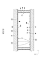
- As shown in FIG. 1A, a pressure-resistant spacer material is prepared, and cut to a predetermined shape using a cutter, such as a diamond wheel and a laser cutter, to thereby form a
spacer body 10. - The spacer material is formed with any one of glass, ceramic, reinforced glass, and various other materials currently used in forming spacers. The
spacer body 10 may be formed in the shape of a bar, a pillar, or various other shapes. A bar-shaped spacer body is illustrated in the drawing. - Alternatively, the
spacer body 10 may be formed of a photosensitive glass material, and completed by patterning it through partial light exposing, heat treating and etching. - As seen in the magnified portion of FIG. 1A, micro-cracks or micro-pores are present at the surface of the completed
spacer body 10, which has a surface roughness of 0.12 - 0.2 µm. - As shown in FIG. 1B, a
resistance layer 12 is formed by coating a resistant material onto the lateral sides of thespacer body 10. Theresistance layer 12 has the role of providing movement routes of electrons such that the electrons colliding against the surface of the spacers flow out to an electron emission unit (not shown) or to a light emission unit (not shown), preventing the spacers from being surface-charged. - The
resistance layer 12 is designed to prevent the electron emission unit and the light emission unit from being short circuited with each other through the spacer, and to provide the movement routes of the electrons. For this purpose, theresistance layer 12 has a specific resistance of roughly 105 - 108Ωcm. For instance, theresistance layer 12 may be formed with Cr2O3. - In order to maintain the above-identified specific resistance value, the
resistance layer 12 may be roughly formed with a thin thickness of 0.5 - 1 µm. Accordingly, theresistance layer 12 may not fill the surface micro-cracks or micro-pores of thespacer body 10 sufficiently, and may be only partially formed on the surface of thespacer body 10 due to the surface roughness of thespacer body 10. - However, as shown in FIG. 1C, a
flattening layer 14 is formed on the surface of theresistance layer 12 with a thickness larger than that of theresistance layer 12. Theflattening layer 14 roughly has a thickness of 1 - 1.5 µm, and sufficiently covers thespacer body 10 and theresistance layer 12 such that it fills the surface micro-cracks and micro-pores of thespacer body 10. Theflattening layer 14 is not influenced by the surface roughness of thespacer body 10 and theresistance layer 12, and has an external surface with an extremely small surface roughness of 0.01 - 0.1 µm - The
flattening layer 14 is formed with an insulating material, or a resistant material having a specific resistance greater than that of theresistance layer 12. For instance, theflattening layer 14 may be formed with polyimide (PI). Theflattening layer 14 may be formed in various ways, such as spraying and dipping, and have the above-identified surface roughness range through the surface treatment process. - With the
spacers 16 according to the present embodiment, the movement routes of electrons are provided through theresistance layer 12 having the above-identified specific resistance value, thereby preventing thespacers 16 from being surface-charged. Furthermore, thespacer 16 prevents the surface of thespacer body 10 based on the dielectric material from being exposed by theflattening layer 14 having the above-identified thickness and surface roughness, and minimizes the surface roughness, thereby preventing the arc discharging with the mounting thereof within the vacuum vessel. - FIG. 2, according to an embodiment of the present invention, is a schematic sectional view of an electron emission display having the above-described spacers.
- As shown in FIG. 2, the electron emission display includes
first substrate 20 andsecond substrate 22 facing each other in parallel at a predetermined distance. A sealingmember 24 is provided at the peripheries of the first andsecond substrates second substrates - The first and
second substrates active area 26 internal to the sealingmember 24 which serves to emit visible rays, and anon-active area 28 surrounding theactive area 26. Anelectron emission unit 200 is provided at theactive area 26 of thefirst substrate 20 to emit electrons, and alight emission unit 300 is provided at the active area of thesecond substrate 22 to emit visible rays. - A plurality of
spacers second substrates spacers 161 are provided in theactive area 26 and thespacers 162 are provided in thenon-active area 28. For explanatory convenience, the spacers placed at theactive area 26 are called thefirst spacers 161, and the spacers placed at thenon-active area 28 are called thesecond spacers 162. - The
first spacers 161 are so small in width that they are not seen from the sight of the user during the operation of the electron emission display. Since the limitation in width of thesecond spacers 162 is not so great as compared to that of thefirst spacers 161, thespacer body 102 of thesecond spacer 162 may be formed to be larger in width than thespacer body 101 of thefirst spacer 161. - The first and
second spacers spacer bodies spacer bodies layers spacer bodies - The internal structure and spacer operation of the FEA type electron emission display will be now explained with reference to FiGs. 3 and 4, and the internal structure and spacer operation of the SCE type electron emission display with reference to FIG. 5.
- As shown in FIGs. 3 and 4, with the FEA type electron emission display, the
electron emission unit 210 includeselectron emission regions 30,cathode electrodes 32, gate electrodes, 34, and a focusingelectrode 36 for focusing the electron beams. - Specifically,
cathode electrodes 32 are stripe-patterned on thefirst substrate 201 in a direction of thefirst substrate 201, and a first insulatinglayer 38 is formed on the entire surface of thefirst substrate 201 such that it covers thecathode electrodes 32.Gate electrodes 34 are stripe-patterned on the first insulatinglayer 38 such that they cross thecathode electrodes 32. - In this embodiment, when the crossed regions of the cathode and
gate electrodes electron emission regions 30 are formed on thecathode electrodes 32 at the respective pixels, andopenings 381 are formed at the first insulatinglayer 38, andopenings 341 are formed at thegate electrodes 34 corresponding to the respectiveelectron emission regions 30 such that theelectron emission regions 30 are exposed on thefirst substrate 201 therethrough. - The
electron emission regions 30 are formed of a material emitting electrons when an electric field is applied thereto under a vacuum atmosphere, such as a carbonaceous material and a nanometer-sized material. For instance, theelectron emission regions 30 may be formed with carbon nanotube, graphite, graphite nanofiber, diamond, diamond-like carbon, fullerene C60, silicon nanowire, or a combination thereof, through screen-printing, direct growth, sputtering, or chemical vapor deposition. - Alternatively, the electron emission regions may be formed with a sharp-pointed tip structure mainly based on molybdenum (Mo) or silicon (Si).
- It is illustrated in the drawings that the circular-shaped
electron emission regions 30 are linearly arranged in the longitudinal direction of thecathode electrodes 32. However, the shape, number per pixel and arrangement of theelectron emission regions 30 are not limited to that illustrated, but may be altered in various manners. - A focusing
electrode 36 is formed on thegate electrodes 34 and the first insulatinglayer 38. A second insulatinglayer 40 is placed under the focusingelectrode 36 to insulate thegate electrodes 34 from the focusingelectrode 36, andopenings 361 are formed at the focusingelectrode 36 andopenings 401 are formed at the second insulatinglayer 40 to pass the electron beams. - The focusing
electrodes 36 have openings corresponding to the respectiveelectron emission regions 30 to separately focus the electrons emitted from the respectiveelectron emission regions 30. Alternatively, oneopening 361 is formed at each pixel to collectively focus the electrons emitted from the pixel. FIG. 3 illustrates the second case. - The
light emission unit 310 includes phosphor layers 42, a black layer disposed between the neighboring phosphor layers 42, and ananode electrode 46 placed on a surface of the phosphor andblack layers - The phosphor layers 42 include red, green and blue phosphor layers 42R, 42G, 42B such that one colored phosphor layer is placed at each crossed region of the cathode and
gate electrodes black layer 42 is placed between the respective phosphor layers 42 in the shape of a matrix to enhance the screen contrast. - The
anode electrode 46 is formed of an aluminum-like metallic layer placed on a surface of the phosphor and theblack layers first substrate 201. Theanode electrode 46 receives from the outside a high voltage required to make the phosphor layers 42 be in a high potential state for accelerating the electron beams, and reflects the visible rays radiated from the phosphor layers 42 to thefirst substrate 201 toward thesecond substrate 221, thereby enhancing the screen luminance. - Alternatively, the anode electrode may be formed with a transparent conductive layer such as indium tin oxide (ITO). In this case, the anode electrode is placed on a surface of the phosphor and
black layers second substrate 221. It is also possible to simultaneously form the metallic layer and the transparent conductive layer as the anode electrode. - The
first spacers 161 correspond to theblack layer 44 such that they do not intrude upon the area of the phosphor layers 42. Thefirst spacer 161 has aspacer body 101 roughly with a surface roughness of 0.12 - 0.2 µm, aresistance layer 121 placed on the lateral side of thespacer body 101 with a thickness of 0.5 - 1 µm and a specific resistance of 105- 108Ωcm, and aflattening layer 141 placed on a surface of theresistance layer 121 roughly with a thickness of 1 - 1.5 µm and a surface roughness of 0.01 - 0.1 µm. - A conductive adhesive layer (not shown) is placed on a surface of the
first spacer 161 directed toward thefirst substrate 201 or a surface of thefirst spacer 161 directed toward thesecond substrate 221 to electrically connect theresistance layer 121 to the focusingelectrode 36 or theresistance layer 121 to theanode electrode 46. - Although not shown in the drawings, second spacers are placed at the non-active area of the first and
second substrates first spacers 161. The second spacers have the same general structure as that of thefirst spacers 161 except for the width of the spacer body thereof. - The above-structured electron emission display is driven by supplying predetermined voltages to the
cathode electrodes 32, thegate electrodes 34, the focusingelectrode 36 and theanode electrode 46 from the outside. - For instance, one of the cathode and
gate electrodes electrode 36 receives a voltage required for focusing the electron beams, for example, 0V or a negative direct current voltage, and theanode electrode 46 receives a voltage required for accelerating electron beams, for example, a positive direct current voltage of several hundreds to several thousands volts. - Electric fields are then formed around the
electron emission regions 30 at the pixels where the voltage difference between the cathode and thegate electrodes electron emission regions 30. The emitted electrons pass through theopenings 361 of the focusingelectrode 36, and are focused at the centers of the bundles of electron beams. The focused electrons are attracted by the high voltage applied to theanode electrode 36, and collide against the phosphor layers 42 at the relevant pixels, thereby exciting the phosphor layers to emit light. - With the above driving process, the electrons emitted from the respective
electron emission regions 30 are diffused at a predetermined diffusion angle even under the operation of the focusingelectrode 36. Accordingly, although some of the electrons collide against the surface of thefirst spacers 161, those electrons flow to the focusingelectrode 36 or theanode electrode 46 through theresistance layer 121, thereby preventing thefirst spacers 161 from being surface-charged. - Furthermore, since the
flattening layer 141 of thefirst spacer 161 prevents the surface of thespacer body 101 based on the dielectric material from being exposed so that the surface charging at the area with noresistance layer 121 may be prevented. Since the first and second spacers have a smooth surface due to the flattening layer, the arc discharging induced by the spacers can be effectively prevented. - As shown in FIG. 5, with an SCE type electron emission display the
electron emission unit 220 includes first andsecond electrodes thin films second electrodes electron emission regions 56 disposed between the first and second conductivethin films - The first and
second electrodes thin films - The
electron emission regions 56 may be formed with micro-cracks provided between the first and second conductivethin films electron emission regions 56 may contain carbon nanotube, graphite, graphite nanofiber, diamond, diamond-like carbon, fullerene C60, or a combination thereof. - The
light emission unit 320 may have the same structure as that of the light emission unit of the previously-described FEA type electron emission display. Thefirst spacers 161 placed at the active area and the second spacers (not shown) placed at the non-active area also have the same structure as that of the spacers of the previously-described electron emission display. For explanatory convenience, like reference numerals will be used for the same structural components as those related to the FEA type electron emission display, and detailed explanation thereof will be omitted. - With the SCE type electron emission display, when predetermined driving voltages are applied to the first and
second electrodes electron emission regions 56 through the first and second conductivethin films anode electrode 46, and directed toward thesecond substrate 222, thereby hitting the phosphor layers 42 to emit light. - With the above driving process, the electrons emitted from the respective
electron emission regions 56 are diffused at a predetermined diffusion angle so that some of the electrons collide against the surface of thefirst spacers 161. However, since those electrons flow to theanode electrode 46 through theresistance layer 121, thefirst spacer 161 may be prevented from being surface-charged. - Furthermore, since the
flattening layer 141 of thefirst spacer 161 prevents the surface of thespacer body 101 from being exposed, the surface charging of thefirst spacers 161 at the area with noresistance layer 121 is prevented. Since the flattening layer has an extremely small surface roughness, the first and second spacers may effectively prevent arc discharging induced by the spacers.
Claims (15)
- A spacer (161, 162) locatable between a first substrate (20, 201, 202) and a second substrate (22, 221, 222), the first substrate (20, 201, 202) and the second substrate (22, 221, 222) together with a sealing member forming a vacuum vessel, the spacer (161, 162) comprising:a spacer body (10, 101, 102);a resistance layer (12, 121, 122) placed on at least one lateral side of the spacer body (10, 101, 102); anda flattening layer (14, 141, 142) covering the resistance layer (12, 121, 122), the flattening layer (14, 141, 142) having a thickness larger than a thickness of the resistance layer (12, 121, 122) and the flattening layer (14, 141, 142) having a surface roughness smaller than a surface roughness of the spacer body (10, 101, 102).
- The spacer of claim 1, wherein the resistance layer (12, 121, 122) has a specific resistance of 105 - 108Ωcm and a thickness of 0.5 - 1 µm.
- The spacer according to one of the preceding claims, wherein the flattening layer (14, 141, 142) has a thickness of 1 - 1.5 µm and a surface roughness of 0.01 - 0.1 µm.
- The spacer according to one of the preceding claims, wherein the flattening layer (14, 141, 142) has a specific resistance greater than a specific resistance of the resistance layer (12, 121, 122).
- The spacer according to one of the preceding claims, wherein the spacer body (10, 101, 102) has a surface roughness of 0.12 µm or more.
- A method of manufacturing a spacer (161, 162), the method comprising:forming a spacer body (10, 101, 102) having a surface with a surface roughness by patterning a spacer body material;forming a resistance layer (12, 121, 122) covering at least one lateral side of the spacer body (10, 101, 102) by coating a resistant material onto the lateral side of the spacer body (10, 101, 102); andforming a flattening layer (14, 141, 142) over the resistance layer (12, 121, 122), the flattening layer (14, 141, 142) having a thickness larger than a thickness of the resistance layer (12, 121, 122) and having a surface roughness smaller than a surface roughness of the spacer body (10, 101, 102).
- The method of claim 6, wherein the resistance layer (12, 121, 122) is formed with a specific resistance of 105 - 108Ωcm and a thickness of 0.5 - 1 µm and/or wherein the flattening layer (14, 141, 142) is formed with a thickness of 1 - 1.5 µm and a surface roughness of 0.01 - 0.1 µm.
- The method according to one of the claims 6 and 7, wherein the flattening layer (14, 141, 142) is formed either by spraying or by dipping, and the step of forming the flattening layer (14, 141, 142) further comprises a step of surface-treating the flattening layer (14, 141, 142).
- The method according to one of the claims 6 - 8, wherein the flattening layer (14, 141, 142) is formed from an insulating material or a material having a specific resistance greater than a specific resistance of the resistance layer (12, 121, 122).
- An electron emission display comprising:a first substrate (20, 201, 202) and a second substrate (22, 221, 222) facing each other, the first substrate (20, 201, 202) and the second substrate (22, 221, 222) with a sealing member forming a vacuum vessel;an electron emission unit (200, 210, 220) provided on the first substrate (20, 201, 202);a light emission unit (300, 310, 320) provided on the second substrate (22, 221, 222); anda plurality of spacers (161, 162) according to one of the claims 1-5 disposed between the first and the second substrates (20, 201, 202, 22, 221, 222).
- The electron emission display of claim 10, wherein the electron emission unit (210) includes cathode electrodes (32) and gate electrodes (34) insulated from each other, and electron emission regions (30) electrically connected to the cathode electrodes (32).
- The electron emission display of claim 11, wherein the electron emission unit (210) further comprises a focusing electrode (36) placed over the cathode electrodes (32) and the gate electrodes (34) such that the focusing electrode (36) is insulated from the cathode electrodes (32) and the gate electrodes (34).
- The electron emission display of claim 10, wherein the electron emission unit comprises:a first conductive thin film and a second conductive thin film spaced from each other;first electrodes electrically connected to the first conductive thin film;second electrodes electrically connected to the second conductive thin film, and electron emission regions disposed between the first conductive thin film and the second conductive thin film.
- The electron emission display according to one of the claims 10-13, wherein the light emission unit (300, 310, 320) comprises:phosphor layers (42R, 42G, 42B),at least one black layer (44) disposed between the phosphor layers (42R, 42G, 42B); andan anode electrode (46) placed on a surface of the phosphor layers (42R, 42G, 42B) and the black layers (44).
- The electron emission display of claim 10, wherein:the first substrate (20, 201, 202) and the second substrate (22, 221, 222) include:an active area (26) having the electron emission unit (200) and the light emission unit (300), respectively;a non-active area (28) placed external to the active area (26), and the spacers (161, 162) include:first spacers (161) placed at the active area (26); andsecond spacers (162) placed at the non-active area (28).
Applications Claiming Priority (1)
| Application Number | Priority Date | Filing Date | Title |
|---|---|---|---|
| KR1020060009328A KR101173859B1 (en) | 2006-01-31 | 2006-01-31 | Spacer and electron emission display device having the same |
Publications (2)
| Publication Number | Publication Date |
|---|---|
| EP1818966A1 true EP1818966A1 (en) | 2007-08-15 |
| EP1818966B1 EP1818966B1 (en) | 2009-08-26 |
Family
ID=38055139
Family Applications (1)
| Application Number | Title | Priority Date | Filing Date |
|---|---|---|---|
| EP07101392A Expired - Fee Related EP1818966B1 (en) | 2006-01-31 | 2007-01-30 | Electron emission display spacer and manufacturing method thereof |
Country Status (6)
| Country | Link |
|---|---|
| US (1) | US7772754B2 (en) |
| EP (1) | EP1818966B1 (en) |
| JP (1) | JP4430652B2 (en) |
| KR (1) | KR101173859B1 (en) |
| CN (1) | CN100576411C (en) |
| DE (1) | DE602007002080D1 (en) |
Families Citing this family (2)
| Publication number | Priority date | Publication date | Assignee | Title |
|---|---|---|---|---|
| KR20090023903A (en) * | 2007-09-03 | 2009-03-06 | 삼성에스디아이 주식회사 | Light emission device and display device using the light emission device as a light source |
| JP5262797B2 (en) * | 2009-02-16 | 2013-08-14 | コニカミノルタビジネステクノロジーズ株式会社 | Image display device |
Citations (3)
| Publication number | Priority date | Publication date | Assignee | Title |
|---|---|---|---|---|
| EP1032014A2 (en) * | 1999-02-25 | 2000-08-30 | Canon Kabushiki Kaisha | Manufacturing method of spacer for electron-beam apparatus and manufacturing method of electron-beam apparatus |
| EP1137041A1 (en) * | 1998-09-08 | 2001-09-26 | Canon Kabushiki Kaisha | Electron beam device, method for producing charging-suppressing member used in the electron beam device, and image forming device |
| US6734608B1 (en) * | 1998-12-11 | 2004-05-11 | Candescent Technologies Corporation | Constitution and fabrication of flat-panel display and porous-faced structure suitable for partial of full use in spacer of flat-panel display |
Family Cites Families (10)
| Publication number | Priority date | Publication date | Assignee | Title |
|---|---|---|---|---|
| JP3302313B2 (en) * | 1996-12-27 | 2002-07-15 | キヤノン株式会社 | Antistatic film, image forming apparatus and method of manufacturing the same |
| CN1282448A (en) | 1997-12-17 | 2001-01-31 | 摩托罗拉公司 | Field emission device having composite spacer |
| US6255772B1 (en) * | 1998-02-27 | 2001-07-03 | Micron Technology, Inc. | Large-area FED apparatus and method for making same |
| US6566794B1 (en) * | 1998-07-22 | 2003-05-20 | Canon Kabushiki Kaisha | Image forming apparatus having a spacer covered by heat resistant organic polymer film |
| JP2000082422A (en) | 1998-09-02 | 2000-03-21 | Canon Inc | Antistatic film for image display device |
| JP3639732B2 (en) | 1998-10-07 | 2005-04-20 | キヤノン株式会社 | Spacer manufacturing method and image display device manufacturing method |
| JP2000251705A (en) | 1999-02-24 | 2000-09-14 | Canon Inc | Manufacture of atmospheric pressure-resistant support structure for electron beam device, atmospheric pressure-resistant support structure for electron beam device and electron beam device |
| US7315115B1 (en) * | 2000-10-27 | 2008-01-01 | Canon Kabushiki Kaisha | Light-emitting and electron-emitting devices having getter regions |
| TWI312166B (en) * | 2001-09-28 | 2009-07-11 | Toppan Printing Co Ltd | Multi-layer circuit board, integrated circuit package, and manufacturing method for multi-layer circuit board |
| KR20070044894A (en) * | 2005-10-26 | 2007-05-02 | 삼성에스디아이 주식회사 | Electron emission display device |
-
2006
- 2006-01-31 KR KR1020060009328A patent/KR101173859B1/en not_active IP Right Cessation
- 2006-11-22 JP JP2006315252A patent/JP4430652B2/en not_active Expired - Fee Related
-
2007
- 2007-01-30 DE DE602007002080T patent/DE602007002080D1/en active Active
- 2007-01-30 CN CN200710006926A patent/CN100576411C/en not_active Expired - Fee Related
- 2007-01-30 US US11/700,749 patent/US7772754B2/en not_active Expired - Fee Related
- 2007-01-30 EP EP07101392A patent/EP1818966B1/en not_active Expired - Fee Related
Patent Citations (3)
| Publication number | Priority date | Publication date | Assignee | Title |
|---|---|---|---|---|
| EP1137041A1 (en) * | 1998-09-08 | 2001-09-26 | Canon Kabushiki Kaisha | Electron beam device, method for producing charging-suppressing member used in the electron beam device, and image forming device |
| US6734608B1 (en) * | 1998-12-11 | 2004-05-11 | Candescent Technologies Corporation | Constitution and fabrication of flat-panel display and porous-faced structure suitable for partial of full use in spacer of flat-panel display |
| EP1032014A2 (en) * | 1999-02-25 | 2000-08-30 | Canon Kabushiki Kaisha | Manufacturing method of spacer for electron-beam apparatus and manufacturing method of electron-beam apparatus |
Also Published As
| Publication number | Publication date |
|---|---|
| DE602007002080D1 (en) | 2009-10-08 |
| CN101013647A (en) | 2007-08-08 |
| US20070176530A1 (en) | 2007-08-02 |
| KR101173859B1 (en) | 2012-08-14 |
| EP1818966B1 (en) | 2009-08-26 |
| US7772754B2 (en) | 2010-08-10 |
| CN100576411C (en) | 2009-12-30 |
| JP2007207747A (en) | 2007-08-16 |
| KR20070078899A (en) | 2007-08-03 |
| JP4430652B2 (en) | 2010-03-10 |
Similar Documents
| Publication | Publication Date | Title |
|---|---|---|
| US20060261725A1 (en) | Electron emission device, electron emission display, and manufacturing method of the electron emission device | |
| EP1696465B1 (en) | Electron emission device and method for manufacturing the same | |
| EP1708226B1 (en) | Electron emission device and electron emission display device using the same | |
| EP1708237B1 (en) | Electron emission device | |
| EP1818966B1 (en) | Electron emission display spacer and manufacturing method thereof | |
| US7911123B2 (en) | Electron emission device and electron emission display using the electron emission device | |
| US7456563B2 (en) | Electron emission display and manufacturing method of the same | |
| US20070182311A1 (en) | Electron emission display | |
| EP1780759B1 (en) | Electron emission device and electron emission display having the same | |
| EP1786020B1 (en) | Electron emission device and display device using the same | |
| US20070114911A1 (en) | Electron emission device, electron emission display device using the same, and method for manufacturing the same | |
| US7772758B2 (en) | Electron emission display including spacers with layers | |
| EP1848021B1 (en) | Vacuum envelope and electron emission display using vacuum envelope | |
| US7468577B2 (en) | Electron emission display having a spacer with inner electrode inserted therein | |
| US7518303B2 (en) | Electron emission device with plurality of lead lines crossing adhesive film | |
| US20070247056A1 (en) | Electron emission display | |
| EP1821329A2 (en) | Electron emission device and electron emission display using the same | |
| EP1780753B1 (en) | Electron emission display | |
| US7750547B2 (en) | Electron emission device with reduced deterioration of screen image quality | |
| EP1780758A1 (en) | Electron emission display | |
| KR20080034621A (en) | Spacer for electron emission display and electron emission display | |
| KR20080006912A (en) | Spacer and electron emission display device with the spacer | |
| KR20070111860A (en) | Electron emission device and electron emission display device using the same | |
| KR20080034622A (en) | Spacer for electron emission display and electron emission display |
Legal Events
| Date | Code | Title | Description |
|---|---|---|---|
| PUAI | Public reference made under article 153(3) epc to a published international application that has entered the european phase |
Free format text: ORIGINAL CODE: 0009012 |
|
| 17P | Request for examination filed |
Effective date: 20070130 |
|
| AK | Designated contracting states |
Kind code of ref document: A1 Designated state(s): AT BE BG CH CY CZ DE DK EE ES FI FR GB GR HU IE IS IT LI LT LU LV MC NL PL PT RO SE SI SK TR |
|
| AX | Request for extension of the european patent |
Extension state: AL BA HR MK YU |
|
| RIN1 | Information on inventor provided before grant (corrected) |
Inventor name: LEE, JAE-HOON Inventor name: CHANG, CHEOL-HYEON Inventor name: SEON, HYEONG-RAE |
|
| AKX | Designation fees paid |
Designated state(s): DE FR GB |
|
| GRAP | Despatch of communication of intention to grant a patent |
Free format text: ORIGINAL CODE: EPIDOSNIGR1 |
|
| GRAS | Grant fee paid |
Free format text: ORIGINAL CODE: EPIDOSNIGR3 |
|
| GRAA | (expected) grant |
Free format text: ORIGINAL CODE: 0009210 |
|
| AK | Designated contracting states |
Kind code of ref document: B1 Designated state(s): DE FR GB |
|
| REG | Reference to a national code |
Ref country code: GB Ref legal event code: FG4D |
|
| REF | Corresponds to: |
Ref document number: 602007002080 Country of ref document: DE Date of ref document: 20091008 Kind code of ref document: P |
|
| PLBE | No opposition filed within time limit |
Free format text: ORIGINAL CODE: 0009261 |
|
| STAA | Information on the status of an ep patent application or granted ep patent |
Free format text: STATUS: NO OPPOSITION FILED WITHIN TIME LIMIT |
|
| 26N | No opposition filed |
Effective date: 20100527 |
|
| PGFP | Annual fee paid to national office [announced via postgrant information from national office to epo] |
Ref country code: GB Payment date: 20130111 Year of fee payment: 7 Ref country code: FR Payment date: 20130215 Year of fee payment: 7 Ref country code: DE Payment date: 20130117 Year of fee payment: 7 |
|
| REG | Reference to a national code |
Ref country code: DE Ref legal event code: R119 Ref document number: 602007002080 Country of ref document: DE |
|
| GBPC | Gb: european patent ceased through non-payment of renewal fee |
Effective date: 20140130 |
|
| REG | Reference to a national code |
Ref country code: DE Ref legal event code: R119 Ref document number: 602007002080 Country of ref document: DE Effective date: 20140801 |
|
| PG25 | Lapsed in a contracting state [announced via postgrant information from national office to epo] |
Ref country code: DE Free format text: LAPSE BECAUSE OF NON-PAYMENT OF DUE FEES Effective date: 20140801 |
|
| REG | Reference to a national code |
Ref country code: FR Ref legal event code: ST Effective date: 20140930 |
|
| PG25 | Lapsed in a contracting state [announced via postgrant information from national office to epo] |
Ref country code: GB Free format text: LAPSE BECAUSE OF NON-PAYMENT OF DUE FEES Effective date: 20140130 Ref country code: FR Free format text: LAPSE BECAUSE OF NON-PAYMENT OF DUE FEES Effective date: 20140131 |