EP1818851A1 - Portable object having a contact interface, and personalisation of contact interface - Google Patents
Portable object having a contact interface, and personalisation of contact interface Download PDFInfo
- Publication number
- EP1818851A1 EP1818851A1 EP06290235A EP06290235A EP1818851A1 EP 1818851 A1 EP1818851 A1 EP 1818851A1 EP 06290235 A EP06290235 A EP 06290235A EP 06290235 A EP06290235 A EP 06290235A EP 1818851 A1 EP1818851 A1 EP 1818851A1
- Authority
- EP
- European Patent Office
- Prior art keywords
- contact interface
- layer
- portable object
- contact
- interface
- Prior art date
- Legal status (The legal status is an assumption and is not a legal conclusion. Google has not performed a legal analysis and makes no representation as to the accuracy of the status listed.)
- Withdrawn
Links
Images
Classifications
-
- G—PHYSICS
- G06—COMPUTING OR CALCULATING; COUNTING
- G06K—GRAPHICAL DATA READING; PRESENTATION OF DATA; RECORD CARRIERS; HANDLING RECORD CARRIERS
- G06K1/00—Methods or arrangements for marking the record carrier in digital fashion
- G06K1/12—Methods or arrangements for marking the record carrier in digital fashion otherwise than by punching
- G06K1/126—Methods or arrangements for marking the record carrier in digital fashion otherwise than by punching by photographic or thermographic registration
-
- G—PHYSICS
- G06—COMPUTING OR CALCULATING; COUNTING
- G06K—GRAPHICAL DATA READING; PRESENTATION OF DATA; RECORD CARRIERS; HANDLING RECORD CARRIERS
- G06K19/00—Record carriers for use with machines and with at least a part designed to carry digital markings
- G06K19/06—Record carriers for use with machines and with at least a part designed to carry digital markings characterised by the kind of the digital marking, e.g. shape, nature, code
- G06K19/067—Record carriers with conductive marks, printed circuits or semiconductor circuit elements, e.g. credit or identity cards also with resonating or responding marks without active components
- G06K19/07—Record carriers with conductive marks, printed circuits or semiconductor circuit elements, e.g. credit or identity cards also with resonating or responding marks without active components with integrated circuit chips
- G06K19/077—Constructional details, e.g. mounting of circuits in the carrier
- G06K19/07743—External electrical contacts
Definitions
- the invention relates to a portable object having at least a contact interface flushing its surface, and to the personalisation of such contact interface.
- the invention applies to any type of smart card or other portable object which holds in the hand , provided that it uses contact pads to connect electrically the chip to the outside world.
- the portable object can be either a pure contact smart card or an hybrid smart card or a dual-interface smart card, for example.
- contacts of the contact interface are currently made of a stack of layers comprising at least a first layer of copper 1, plated on both sides by a second layer of nickel 2, which is also plated on both sides by an upper layer 3 of either gold or palladium.
- the contact interface of the currently commercialised electronic modules exist only in two colours. Indeed, the surface of the contact interface is either yellow-gold or silver-grey, depending on the upper conductive layer of the contacts.
- a known process for colouring the surface of a contact interface consists in covering the spaces between the contacts by a stencil in order to prevent any later short-circuit and then, applying a conductive lacquer comprising pigments on the contacts.
- the stencil has to be positioned with precision before the application of the conductive lacquer, so that the process is time consuming and increases the cost of the module.
- the use of a stencil, for each module to colour, and the lacquer components increase also substantially the cost of the module.
- a problem intended to be solved by the invention is to provide a method of personalization of an electronic module comprising a contact interface, said method being an alternative solution with those which already exist, allowing better productivity and cost reduction.
- First step A consists in taking a conventional module having a contact interface either with gold-plated finish 10 or with palladium-plated finish 11.
- a second step B the whole surface of the interface contact 13 is covered by a conductive coloured layer.
- this layer comprises a ceramic of Tin-doped Indium oxide (ITO ceramic). Such ceramic is known as having an excellent conductivity.
- This layer allows to keep properties compatible with the current qualification plan of the electronic module.
- This coating layer is preferably applied on the surface of the contact interface by sputtering.
- the thickness of this layer is limited by the dimensions of the portable object in which the module is embedded because the contact interface has to flush the surface of the portable object. For this reason, the thickness of the applied layer is preferably less than 1 ⁇ m.
- This second step leads to the creation of electric short-circuits in the areas 14 located between each contact 13 of the contact interface. These short-circuits are removed in a further step C. For that, the layer applied is removed in these spaces between the contacts of the contact interface, for creating insulation lines 15. This step of removal is advantageously carried out by means of a laser.
- the laser used is for example a YAG laser.
- other lasers may be used such as, for example, SHG or THG lasers.
- the contact interface obtained, after the step C, comprises contacts 13, covered by a conducting coloured layer, well isolated the ones from the others by lines 15.
- An optional step D can be performed simultaneously with step C of removal of the coating layer, in the inter-contact areas 15.
- This optional step allows to apply any kind of logo and/or text 16 required onto the contact interface.
- the laser beam is also used to remove the additional coloured coating layer on at least one contact 13 of the interface, in order to reveal the initial colour of the upper gold or palladium layer of the contact, and thus creating a logo and/or text for distinction purposes.
- This further optional step is very interesting because it does not involve the engraving of initial upper layers, of gold or palladium, composing the contacts, said engraving revealing the lower layer of nickel and being able to lead to lower corrosion resistance and damage electrical properties of contacts.
- gold and palladium being metals nobler than nickel, when the layer of nickel is engraved, the corrosion of the least noble metal (i.e. nickel) is accelerate with the profit of the noblest metal (i.e. gold or palladium).
- An electronic module is inserted in a cavity provided in a portable object, in such a manner that its contact plate flushes the surface of the portable object.
- the coloration and the personalization of the electronic module, according to the invention, can be made either before or after its insertion in the portable object.
- the portable object can be either a pure contact smart card or an hybrid smart card or a dual-interface smart card, for example.
- the portable object may comprise more than one personalized module.
Landscapes
- Engineering & Computer Science (AREA)
- Physics & Mathematics (AREA)
- General Physics & Mathematics (AREA)
- Theoretical Computer Science (AREA)
- Computer Hardware Design (AREA)
- Microelectronics & Electronic Packaging (AREA)
- Credit Cards Or The Like (AREA)
Abstract
The invention relates to a portable object having at least a contact interface flushing its surface, and to the personalisation of such contact interface (10, 11). The method of personalization comprises the steps of :
- applying a conductive coloured layer on the whole surface of the contact interface (10, 11) and,
- removing the applied layer at least in spaces (15) between the contacts (13) of the contact interface.
- applying a conductive coloured layer on the whole surface of the contact interface (10, 11) and,
- removing the applied layer at least in spaces (15) between the contacts (13) of the contact interface.
Description
- The invention relates to a portable object having at least a contact interface flushing its surface, and to the personalisation of such contact interface.
- The invention applies to any type of smart card or other portable object which holds in the hand , provided that it uses contact pads to connect electrically the chip to the outside world. The portable object can be either a pure contact smart card or an hybrid smart card or a dual-interface smart card, for example.
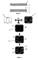
- As illustrated in figure 1, contacts of the contact interface are currently made of a stack of layers comprising at least a first layer of
copper 1, plated on both sides by a second layer ofnickel 2, which is also plated on both sides by anupper layer 3 of either gold or palladium. Thus, the contact interface of the currently commercialised electronic modules exist only in two colours. Indeed, the surface of the contact interface is either yellow-gold or silver-grey, depending on the upper conductive layer of the contacts. - Nowadays, there is a strong request for making fully personalized portable object, namely as well as on the surface of a card body as on the surface of the module. Such full personalization is particularly requested because it allows to obtain easily distinguishable products.
- Today, a known process for colouring the surface of a contact interface consists in covering the spaces between the contacts by a stencil in order to prevent any later short-circuit and then, applying a conductive lacquer comprising pigments on the contacts.
- However, the stencil has to be positioned with precision before the application of the conductive lacquer, so that the process is time consuming and increases the cost of the module. In addition, the use of a stencil, for each module to colour, and the lacquer components increase also substantially the cost of the module.
- Considering the above, a problem intended to be solved by the invention is to provide a method of personalization of an electronic module comprising a contact interface, said method being an alternative solution with those which already exist, allowing better productivity and cost reduction.
- The solution of the invention to this problem relates to the fact that the method comprises the steps of :
- applying a conductive coloured layer on the whole surface of the contact interface and,
- removing the applied layer at least in spaces between the contacts of the contact interface.
- Thus, an additional stencil is not required anymore.
- For a better understanding of the present invention, reference will now be made, by way of example, to the following description of the invention and to the accompanying drawings, in which:
- figure 1, already described, is a schematic cross-section illustrating the composition layers of a contact of a conventional electronic module ;
- figure 2 is a front view of the surface of a contact interface at different steps of a personalization process according to the invention.
- In figure 2, are schematized the different steps of the personalization of a contact interface. First step A consists in taking a conventional module having a contact interface either with gold-plated
finish 10 or with palladium-platedfinish 11. - In a second step B, the whole surface of the
interface contact 13 is covered by a conductive coloured layer. Preferably, this layer comprises a ceramic of Tin-doped Indium oxide (ITO ceramic). Such ceramic is known as having an excellent conductivity. This layer allows to keep properties compatible with the current qualification plan of the electronic module. This coating layer is preferably applied on the surface of the contact interface by sputtering. - In this case, coloration is given by light reflection and refraction of the ITO ceramic. Consequently various colours are obtained depending on the thickness of the sputtered layer. Moreover, the coloration depends also from the specific nature and colour of the substrate, namely the gold-plated or the palladium-plated contact interface. However, the thickness of this layer is limited by the dimensions of the portable object in which the module is embedded because the contact interface has to flush the surface of the portable object. For this reason, the thickness of the applied layer is preferably less than 1µm.
- This second step leads to the creation of electric short-circuits in the
areas 14 located between eachcontact 13 of the contact interface. These short-circuits are removed in a further step C. For that, the layer applied is removed in these spaces between the contacts of the contact interface, for creatinginsulation lines 15. This step of removal is advantageously carried out by means of a laser. - The laser used is for example a YAG laser. However, other lasers may be used such as, for example, SHG or THG lasers.
- The contact interface obtained, after the step C, comprises
contacts 13, covered by a conducting coloured layer, well isolated the ones from the others bylines 15. - An optional step D can be performed simultaneously with step C of removal of the coating layer, in the
inter-contact areas 15. This optional step allows to apply any kind of logo and/ortext 16 required onto the contact interface. For that, the laser beam is also used to remove the additional coloured coating layer on at least onecontact 13 of the interface, in order to reveal the initial colour of the upper gold or palladium layer of the contact, and thus creating a logo and/or text for distinction purposes. - This further optional step is very interesting because it does not involve the engraving of initial upper layers, of gold or palladium, composing the contacts, said engraving revealing the lower layer of nickel and being able to lead to lower corrosion resistance and damage electrical properties of contacts. Indeed, gold and palladium being metals nobler than nickel, when the layer of nickel is engraved, the corrosion of the least noble metal (i.e. nickel) is accelerate with the profit of the noblest metal (i.e. gold or palladium).
- An electronic module is inserted in a cavity provided in a portable object, in such a manner that its contact plate flushes the surface of the portable object. The coloration and the personalization of the electronic module, according to the invention, can be made either before or after its insertion in the portable object.
- The portable object can be either a pure contact smart card or an hybrid smart card or a dual-interface smart card, for example. The portable object may comprise more than one personalized module.
Claims (7)
- A method of personalization of an electronic module comprising a contact interface (10, 11), said method comprising the steps of :- applying a conductive coloured layer on the whole surface of the contact interface (10, 11) and,- removing the applied layer at least in spaces (15) between the contacts (13) of the contact interface.
- A method as claimed in claim 1, wherein the conductive coloured layer comprises a ITO ceramic.
- A method as claimed in claim 1 or 2, wherein the thickness of the conductive coloured layer is less than 1µm.
- A method as claimed in claim 2, wherein the conductive coloured layer is applied by sputtering.
- A method as claimed in claim 1, wherein the applied layer is removed by means of a laser beam.
- A method as claimed in claim 5, wherein the laser is a YAG laser.
- A portable object comprising at least one embedded electronic module whose contact interface flushes the surface of said portable object, wherein the contact interface of the module is personalized according to the method as claimed in previous claims 1 to 6.
Priority Applications (2)
| Application Number | Priority Date | Filing Date | Title |
|---|---|---|---|
| EP06290235A EP1818851A1 (en) | 2006-02-09 | 2006-02-09 | Portable object having a contact interface, and personalisation of contact interface |
| PCT/IB2007/000300 WO2007091158A1 (en) | 2006-02-09 | 2007-02-08 | Portable object having a contact interface, and coloration of contact interface |
Applications Claiming Priority (1)
| Application Number | Priority Date | Filing Date | Title |
|---|---|---|---|
| EP06290235A EP1818851A1 (en) | 2006-02-09 | 2006-02-09 | Portable object having a contact interface, and personalisation of contact interface |
Publications (1)
| Publication Number | Publication Date |
|---|---|
| EP1818851A1 true EP1818851A1 (en) | 2007-08-15 |
Family
ID=36282951
Family Applications (1)
| Application Number | Title | Priority Date | Filing Date |
|---|---|---|---|
| EP06290235A Withdrawn EP1818851A1 (en) | 2006-02-09 | 2006-02-09 | Portable object having a contact interface, and personalisation of contact interface |
Country Status (2)
| Country | Link |
|---|---|
| EP (1) | EP1818851A1 (en) |
| WO (1) | WO2007091158A1 (en) |
Citations (3)
| Publication number | Priority date | Publication date | Assignee | Title |
|---|---|---|---|---|
| US6049055A (en) * | 1996-02-23 | 2000-04-11 | Orga Kartensysteme Gmbh | Method of producing a smart card |
| WO2000031686A1 (en) * | 1998-11-24 | 2000-06-02 | Gemplus | Method for making a flush chip card using a laser engraving step and resulting chip card |
| EP1411467A1 (en) * | 2002-10-17 | 2004-04-21 | Giesecke & Devrient GmbH | Portable data carrier with display |
-
2006
- 2006-02-09 EP EP06290235A patent/EP1818851A1/en not_active Withdrawn
-
2007
- 2007-02-08 WO PCT/IB2007/000300 patent/WO2007091158A1/en not_active Ceased
Patent Citations (3)
| Publication number | Priority date | Publication date | Assignee | Title |
|---|---|---|---|---|
| US6049055A (en) * | 1996-02-23 | 2000-04-11 | Orga Kartensysteme Gmbh | Method of producing a smart card |
| WO2000031686A1 (en) * | 1998-11-24 | 2000-06-02 | Gemplus | Method for making a flush chip card using a laser engraving step and resulting chip card |
| EP1411467A1 (en) * | 2002-10-17 | 2004-04-21 | Giesecke & Devrient GmbH | Portable data carrier with display |
Also Published As
| Publication number | Publication date |
|---|---|
| WO2007091158A1 (en) | 2007-08-16 |
Similar Documents
| Publication | Publication Date | Title |
|---|---|---|
| CN104918421A (en) | Manufacturing method for PCB golden finger | |
| CN1180365C (en) | Chip card manufacturing method | |
| US20120201994A1 (en) | Functional laminate | |
| WO2000055808A1 (en) | Method for making an electronic device such as a contactless card | |
| CN1528109A (en) | Method for manufacturing printed circuit and planar antenna manufactured using said printed circuit | |
| CN100359682C (en) | Electronic label and its manufacturing method | |
| CN108207082A (en) | A kind of method for laser machining line slot and making two-sided printed circuit board of sunkening cord | |
| CN101594740A (en) | Circuit board with embedded electronic device and method thereof | |
| US6783077B1 (en) | Conductor track supporting layer for laminating inside a chip card, chip card comprising a conductor track supporting layer, and method for producing a chip card | |
| JPH0750801B2 (en) | Method of making a hybrid circuit device with an array of the same electronic components | |
| CN1254858C (en) | Electronic chip assembly with integrated circuit and manufacturing method thereof | |
| EP1491078B1 (en) | Multi-layer integrated circuit package | |
| WO2007091158A1 (en) | Portable object having a contact interface, and coloration of contact interface | |
| WO2015024821A1 (en) | Electronic device having a memory | |
| CN111465721B (en) | Circuit, electronic module of a chip card implemented on the circuit and method for implementing such a circuit | |
| CN104866132A (en) | Manufacturing method of touch sensor and touch sensor | |
| EP4472359A1 (en) | Wiring board | |
| KR102913578B1 (en) | Optimized process for graphic personalization of chip card modules and acquired chip card modules | |
| CN109890145A (en) | A kind of keypad gold plating method | |
| CN115668494B (en) | Method for manufacturing electronic chip card module circuit with colored contacts and circuit produced by the method | |
| WO2008040307A2 (en) | Method for producing an arrangement of optoelectronic components, and arrangement of optoelectronic components | |
| CN111491458A (en) | Circuit board and manufacturing method thereof | |
| JPH1146061A (en) | Manufacture of printed-wiring board | |
| US20230064497A1 (en) | Resistor-embedded circuit board and method for processing the resistor-embedded circuit board | |
| CN103731998A (en) | Method for manufacturing printed circuit board |
Legal Events
| Date | Code | Title | Description |
|---|---|---|---|
| PUAI | Public reference made under article 153(3) epc to a published international application that has entered the european phase |
Free format text: ORIGINAL CODE: 0009012 |
|
| AK | Designated contracting states |
Kind code of ref document: A1 Designated state(s): AT BE BG CH CY CZ DE DK EE ES FI FR GB GR HU IE IS IT LI LT LU LV MC NL PL PT RO SE SI SK TR |
|
| AX | Request for extension of the european patent |
Extension state: AL BA HR MK YU |
|
| AKX | Designation fees paid | ||
| REG | Reference to a national code |
Ref country code: DE Ref legal event code: 8566 |
|
| STAA | Information on the status of an ep patent application or granted ep patent |
Free format text: STATUS: THE APPLICATION IS DEEMED TO BE WITHDRAWN |
|
| 18D | Application deemed to be withdrawn |
Effective date: 20080216 |