EP1817789B1 - Mass spectrometer - Google Patents
Mass spectrometer Download PDFInfo
- Publication number
- EP1817789B1 EP1817789B1 EP05811474A EP05811474A EP1817789B1 EP 1817789 B1 EP1817789 B1 EP 1817789B1 EP 05811474 A EP05811474 A EP 05811474A EP 05811474 A EP05811474 A EP 05811474A EP 1817789 B1 EP1817789 B1 EP 1817789B1
- Authority
- EP
- European Patent Office
- Prior art keywords
- electrodes
- ions
- ion
- voltage
- array
- Prior art date
- Legal status (The legal status is an assumption and is not a legal conclusion. Google has not performed a legal analysis and makes no representation as to the accuracy of the status listed.)
- Active
Links
- 150000002500 ions Chemical class 0.000 claims abstract description 372
- 230000001052 transient effect Effects 0.000 claims abstract description 40
- 238000013467 fragmentation Methods 0.000 claims description 48
- 238000006062 fragmentation reaction Methods 0.000 claims description 48
- 238000006243 chemical reaction Methods 0.000 claims description 34
- 238000000034 method Methods 0.000 claims description 17
- 238000005036 potential barrier Methods 0.000 claims description 15
- 239000000758 substrate Substances 0.000 claims description 15
- 230000004323 axial length Effects 0.000 claims description 13
- 230000001133 acceleration Effects 0.000 claims description 6
- 230000000694 effects Effects 0.000 claims description 6
- 238000005040 ion trap Methods 0.000 claims description 6
- 238000000816 matrix-assisted laser desorption--ionisation Methods 0.000 claims description 6
- 230000005540 biological transmission Effects 0.000 claims description 5
- 238000003795 desorption Methods 0.000 claims description 5
- 238000000926 separation method Methods 0.000 claims description 5
- 238000010265 fast atom bombardment Methods 0.000 claims description 4
- 238000004992 fast atom bombardment mass spectroscopy Methods 0.000 claims description 4
- 238000009616 inductively coupled plasma Methods 0.000 claims description 4
- 238000001871 ion mobility spectroscopy Methods 0.000 claims description 4
- 238000001698 laser desorption ionisation Methods 0.000 claims description 4
- 239000000126 substance Substances 0.000 claims description 4
- KXGFMDJXCMQABM-UHFFFAOYSA-N 2-methoxy-6-methylphenol Chemical compound [CH]OC1=CC=CC([CH])=C1O KXGFMDJXCMQABM-UHFFFAOYSA-N 0.000 claims description 3
- RYGMFSIKBFXOCR-UHFFFAOYSA-N Copper Chemical compound [Cu] RYGMFSIKBFXOCR-UHFFFAOYSA-N 0.000 claims description 3
- 238000004252 FT/ICR mass spectrometry Methods 0.000 claims description 3
- 229910052802 copper Inorganic materials 0.000 claims description 3
- 239000010949 copper Substances 0.000 claims description 3
- 238000000688 desorption electrospray ionisation Methods 0.000 claims description 3
- 239000003822 epoxy resin Substances 0.000 claims description 3
- 239000011152 fibreglass Substances 0.000 claims description 3
- 239000012212 insulator Substances 0.000 claims description 3
- 229920001568 phenolic resin Polymers 0.000 claims description 3
- 239000005011 phenolic resin Substances 0.000 claims description 3
- 239000004033 plastic Substances 0.000 claims description 3
- 229920000647 polyepoxide Polymers 0.000 claims description 3
- 102100022704 Amyloid-beta precursor protein Human genes 0.000 claims description 2
- 208000035699 Distal ileal obstruction syndrome Diseases 0.000 claims description 2
- 101000823051 Homo sapiens Amyloid-beta precursor protein Proteins 0.000 claims description 2
- XUIMIQQOPSSXEZ-UHFFFAOYSA-N Silicon Chemical compound [Si] XUIMIQQOPSSXEZ-UHFFFAOYSA-N 0.000 claims description 2
- 239000008186 active pharmaceutical agent Substances 0.000 claims description 2
- DZHSAHHDTRWUTF-SIQRNXPUSA-N amyloid-beta polypeptide 42 Chemical compound C([C@@H](C(=O)N[C@@H](C)C(=O)N[C@@H](CCC(O)=O)C(=O)N[C@@H](CC(O)=O)C(=O)N[C@H](C(=O)NCC(=O)N[C@@H](CO)C(=O)N[C@@H](CC(N)=O)C(=O)N[C@@H](CCCCN)C(=O)NCC(=O)N[C@@H](C)C(=O)N[C@H](C(=O)N[C@@H]([C@@H](C)CC)C(=O)NCC(=O)N[C@@H](CC(C)C)C(=O)N[C@@H](CCSC)C(=O)N[C@@H](C(C)C)C(=O)NCC(=O)NCC(=O)N[C@@H](C(C)C)C(=O)N[C@@H](C(C)C)C(=O)N[C@@H]([C@@H](C)CC)C(=O)N[C@@H](C)C(O)=O)[C@@H](C)CC)C(C)C)NC(=O)[C@H](CC=1C=CC=CC=1)NC(=O)[C@@H](NC(=O)[C@H](CC(C)C)NC(=O)[C@H](CCCCN)NC(=O)[C@H](CCC(N)=O)NC(=O)[C@H](CC=1N=CNC=1)NC(=O)[C@H](CC=1N=CNC=1)NC(=O)[C@@H](NC(=O)[C@H](CCC(O)=O)NC(=O)[C@H](CC=1C=CC(O)=CC=1)NC(=O)CNC(=O)[C@H](CO)NC(=O)[C@H](CC(O)=O)NC(=O)[C@H](CC=1N=CNC=1)NC(=O)[C@H](CCCNC(N)=N)NC(=O)[C@H](CC=1C=CC=CC=1)NC(=O)[C@H](CCC(O)=O)NC(=O)[C@H](C)NC(=O)[C@@H](N)CC(O)=O)C(C)C)C(C)C)C1=CC=CC=C1 DZHSAHHDTRWUTF-SIQRNXPUSA-N 0.000 claims description 2
- 238000000132 electrospray ionisation Methods 0.000 claims description 2
- PXHVJJICTQNCMI-RNFDNDRNSA-N nickel-63 Chemical compound [63Ni] PXHVJJICTQNCMI-RNFDNDRNSA-N 0.000 claims description 2
- 238000004150 penning trap Methods 0.000 claims description 2
- 230000002285 radioactive effect Effects 0.000 claims description 2
- 229910052710 silicon Inorganic materials 0.000 claims description 2
- 239000010703 silicon Substances 0.000 claims description 2
- 238000010494 dissociation reaction Methods 0.000 description 12
- 230000005593 dissociations Effects 0.000 description 12
- 239000012634 fragment Substances 0.000 description 11
- 238000003491 array Methods 0.000 description 4
- 230000005855 radiation Effects 0.000 description 4
- 238000001360 collision-induced dissociation Methods 0.000 description 3
- 230000005684 electric field Effects 0.000 description 3
- 230000032258 transport Effects 0.000 description 3
- 102000004190 Enzymes Human genes 0.000 description 2
- 108090000790 Enzymes Proteins 0.000 description 2
- 230000004888 barrier function Effects 0.000 description 2
- 230000008901 benefit Effects 0.000 description 2
- 230000015556 catabolic process Effects 0.000 description 2
- 238000006731 degradation reaction Methods 0.000 description 2
- 238000001211 electron capture detection Methods 0.000 description 2
- 238000001077 electron transfer detection Methods 0.000 description 2
- 238000001976 enzyme digestion Methods 0.000 description 2
- 230000001965 increasing effect Effects 0.000 description 2
- 230000037427 ion transport Effects 0.000 description 2
- 230000005405 multipole Effects 0.000 description 2
- 230000007935 neutral effect Effects 0.000 description 2
- 238000004088 simulation Methods 0.000 description 2
- 238000000065 atmospheric pressure chemical ionisation Methods 0.000 description 1
- 230000008859 change Effects 0.000 description 1
- 238000000451 chemical ionisation Methods 0.000 description 1
- 238000001816 cooling Methods 0.000 description 1
- 238000000766 differential mobility spectroscopy Methods 0.000 description 1
- 238000001962 electrophoresis Methods 0.000 description 1
- 230000001939 inductive effect Effects 0.000 description 1
- 230000001788 irregular Effects 0.000 description 1
- 238000004949 mass spectrometry Methods 0.000 description 1
- 239000000203 mixture Substances 0.000 description 1
- 230000009467 reduction Effects 0.000 description 1
- 238000011144 upstream manufacturing Methods 0.000 description 1
Images


Classifications
-
- H—ELECTRICITY
- H01—ELECTRIC ELEMENTS
- H01J—ELECTRIC DISCHARGE TUBES OR DISCHARGE LAMPS
- H01J49/00—Particle spectrometers or separator tubes
- H01J49/02—Details
- H01J49/06—Electron- or ion-optical arrangements
- H01J49/062—Ion guides
- H01J49/065—Ion guides having stacked electrodes, e.g. ring stack, plate stack
-
- H—ELECTRICITY
- H01—ELECTRIC ELEMENTS
- H01J—ELECTRIC DISCHARGE TUBES OR DISCHARGE LAMPS
- H01J49/00—Particle spectrometers or separator tubes
- H01J49/02—Details
- H01J49/06—Electron- or ion-optical arrangements
-
- H—ELECTRICITY
- H01—ELECTRIC ELEMENTS
- H01J—ELECTRIC DISCHARGE TUBES OR DISCHARGE LAMPS
- H01J9/00—Apparatus or processes specially adapted for the manufacture, installation, removal, maintenance of electric discharge tubes, discharge lamps, or parts thereof; Recovery of material from discharge tubes or lamps
- H01J9/02—Manufacture of electrodes or electrode systems
- H01J9/14—Manufacture of electrodes or electrode systems of non-emitting electrodes
-
- H—ELECTRICITY
- H01—ELECTRIC ELEMENTS
- H01J—ELECTRIC DISCHARGE TUBES OR DISCHARGE LAMPS
- H01J9/00—Apparatus or processes specially adapted for the manufacture, installation, removal, maintenance of electric discharge tubes, discharge lamps, or parts thereof; Recovery of material from discharge tubes or lamps
- H01J9/02—Manufacture of electrodes or electrode systems
- H01J9/18—Assembling together the component parts of electrode systems
Definitions
- the present invention relates to a device which may comprise an ion guide, an ion mobility spectrometer or separator or a collision, fragmentation or reaction device.
- the device preferably forms part of a mass spectrometer.
- the present Invention also relates to a method of guiding ions, a method of ion mobility spectrometry or ion mobility separation and a method of colliding, fragmenting or reacting ions.
- the preferred embodiment relates to an ion guide comprising a stack of layers of intermediate planar, plate or mesh electrodes.
- the ion guide further comprises an array of upper electrodes and an array of lower electrodes.
- One or more transient DC voltages or potentials or one or more transient DC voltage or potential waveforms are applied to the array of upper electrodes and the array of lower electrodes in order to urge ions along and through at least a portion of the preferred ion guide.
- Multipole rod set ion guides comprising four, six or eight parallel rods which are equi-spaced about a circular circumference.
- the rods are all maintained at substantially the same DC voltage.
- a two-phase RF voltage is also applied to the rods with adjacent rods being supplied with opposite phases of the RF voltage.
- the RF voltage applied to the rods causes a symmetrical effective radial pseudo-potential well to be generated within the space circumscribed by the rods.
- the radial pseudo-potential well causes Ions to be confined radially within the ion guide.
- the ion guide may be maintained at a relatively high pressure and can result in a reduction in the Ion radial density distribution due to collisional cooling of ions with background gas molecules.
- the multipole rod set ion guide may be arranged to confine, transport and focus ions in the presence of background gas.
- the known rod set ion guide may be used, for example, to couple an Atmospheric Pressure ion source to a mass analyser which must be maintained at relatively low pressure.
- ion guide which comprises a plurality or stack of ring electrodes having apertures through which ions are transmitted in use. Opposite phases of a two-phase AC or RF voltage are applied to adjacent electrodes.
- the ion guide may comprise an ion tunnel ion guide comprising electrodes which have apertures which are all substantially the same size or diameter.
- the ion guide may comprise an ion funnel ion guide comprising a plurality of electrodes which have apertures which progressively decrease in diameter along the axial length of the ion guide.
- Ion guide which comprises a stack or a plurality of layers of intermediate planar electrodes.
- the plurality of intermediate planar electrodes are bounded by a single upper planar electrode on one side and a single lower planar electrode on an opposed side.
- Each layer of intermediate planar electrodes comprises two longitudinal electrodes.
- the two longitudinal electrodes in any layer are supplied with the same phase of a two-phase RF voltage.
- Adjacent layers of intermediate planar electrodes are supplied with opposite phases of the two-phase RF voltage.
- the RF voltage applied to the layers of intermediate planar electrodes causes a pseudo-potential well to be generated which acts to confine ions between the longitudinal electrodes within the ion guide in the horizontal radial direction.
- Voltages are applied to the upper and lower single planar electrodes in order to confine ions within the ion guide in the vertical radial direction.
- the known ion guide comprising a stack of layers of intermediate planar electrodes and single upper and lower planar electrodes is particularly advantageous compared to other known ion guides in that various complex and efficient ion transport volumes or geometries can be provided that would be otherwise be very difficult to provide using a rod set ion guide or an ion guide comprising a plurality of ring electrodes.
- Ion guides comprising a stack or plurality of layers of intermediate planar electrodes can be relatively easily designed so as to transport ions along relatively convoluted or potentially complex ion paths.
- a further advantage of an ion guide comprising a plurality of layers of intermediate planar electrodes is that the shape and/or area of the ion confinement volume can be arranged to vary along the length of the ion guide. This enables the ion guide to effectively couple two components of a mass spectrometer which may have different ion-optical acceptance profiles.
- an ion guide comprising a plurality of layers of intermediate planar electrodes may be arranged so that two or more separate ion guides merge into a single ion guide.
- an ion guide comprising a plurality of layers of intermediate planar electrodes may be arranged so that an ion guide divides into two or more separate ion guides.
- the known ion guide comprising a plurality of layers of intermediate planar electrodes and single upper and lower planar electrodes suffers from the problem that collisions between ions and background gas molecules present within the ion guide may reduce the kinetic energy of the ions as they pass through the ion guide. This can have the effect of increasing the transit times of ions as they pass through the ion guide.
- the first array of first electrodes preferably comprises at least 2, 3, 4, 5, 6, 7, 8. 9, 10, 11, 12, 13, 14, 15, 16, 17, 18, 19, 20 or more than 20 electrodes.
- the first array of first electrodes may comprise: (i) a printed circuit board, printed wiring board or etched wiring board; (ii) a plurality of conductive traces applied or laminated onto a non-conductive substrate; (iii) a plurality of copper or metallic electrodes arranged on a substrate; (iv) a screen printed, photoengraved, etched or milled printed circuit board; (v) a plurality of electrodes arranged on a paper substrate impregnated with phenolic resin; (vi) a plurality of electrodes arranged on a fibreglass mat impregnated within an epoxy resin; (vii) a plurality of electrodes arranged on a plastic substrate; or (viii) a plurality of electrodes arranged on a substrate.
- At least 5%. 10%, 15%, 20%, 25%, 30%, 35%, 40%, 45%, 50%, 55%, 60%, 65%, 70%, 75%, 80%, 85%, 90%, 95% or 100% of the first electrodes have an axial centre to centre spacing selected from the group consisting of: (i) ⁇ 1 mm; (ii) 1-2 mm; (iii) 2-3 mm; (Iv) 3-4 mm; (v) 4-5 mm; (vi) 5-6 mm; (vii) 6-7 mm; (viii) 7-8 mm; (Ix) 8-9 mm; (x) 9-10 mm; (xi) 10-11 mm; (xii) 11-12 mm; (xiii) 12-13 mm; (xiv) 13-14 mm; (xv) 14-15 mm; (xvi) 15-16 mm; (xvii) 16-17 mm; (xviii) 17-18 mm; (xix) 18-19 mm; (xx) 19-20 mm;
- At least 5%, 10%, 15%, 20%, 25%, 30%. 35%, 40%, 45%, 50%, 55%, 60%, 65%, 70%, 75%, 80%, 85%, 90%, 95% or 100% of the first electrodes preferably have an axial length selected from the group consisting of: (i) ⁇ 1 mm; (ii) 1-2 mm; (iii) 2-3 mm; (iv) 3-4 mm; (v) 4-5 mm; (vi) 5-6 mm; (vii) 6-7 mm; (viii) 7-8 mm; (ix) 8-9 mm; (x) 9-10 mm; (xi) 10-11 mm; (xii) 11-12 mm; (xiii) 12-13 mm; (xiv) 13-14 mm; (xv) 14-15 mm; (xvi) 15-16 mm; (xvii) 16-17 mm; (xviii) 17-18 mm; (xix) 18-19 mm; (xx) 19-20 mm; and (xxi)
- At least 5%, 10%, 15%, 20%, 25%, 30%. 35%, 40%, 45%, 50%, 55%, 60%, 65%, 70%, 75%, 80%, 85%, 90%, 95% or 100% of the first electrodes have a width selected from the group consisting of: (i) ⁇ 1 mm; (ii) 1-2 mm; (iii) 2-3 mm; (iv) 3-4 mm; (v) 4-5 mm; (vi) 5-6 mm; (vii) 6-7 mm; (viii) 7-8 mm; (ix) 8-9 mm; (x) 9-10 mm; (xi) 10-11 mm; (xii) 11-12 mm; (xiii) 12-13 mm; (xiv) 13-14 mm; (xv) 14-15 mm; (xvi) 15-16 mm; (xvii) 16-17 mm; (xviii) 17-18 mm; (xix) 18-19 mm; (xx) 19-20 mm; and (xxi)
- the first electrodes preferably have a thickness selected from the group consisting of: (i) ⁇ 0.01 mm; (ii) 0.01-0.1 mm; (iii) 0.1-0.2 mm; (iv) 0.2-0.3 mm; (v) 0.3-0.4 mm; (vi) 0.4-0.5 mm; (vii) 0.5-0.6 mm; (viii) 0.6-0.7 mm; (ix) 0.7-0.8 mm; (x) 0.8-0.9 mm: (xi) 0.9-1.0 mm; (xii) 1-2 mm; (xiii) 2-3 mm; (xiv) 3-4 mm; (xv) 4-5 mm; and (xvi) > 5 mm.
- 60%, 65%, 10%; 75%, 80%; 85%, 90%, 95% or 100% of the first electrodes are preferably biased, in use, at a first bias DC voltage or potential with respect to the mean or average voltage or potential of at least some or all of the intermediate planar, plate or mesh electrodes.
- the first DC bias voltage or potential is preferably selected from the group consisting of: (i) less than -10V; (ii) -9 to -8V; (iii) -8 to -7V; (iv) -7 to -6V; (v) -6 to -5V; (vi) -5 to -4V; (vii) -4 to -3V; (viii) -3 to -2V; (ix) -2 to -1V; (x) -1 to 0V; (xi) 0 to 1V; (xii) 1 to 2V; (xiii) 2 to 3V; (xiv) 3 to 4V; (xv) 4 to 5V; (xvi) 5 to 6V; (xvii) 6 to 7V; (xviii) 7 to 8V; (xix) 8 to 9V; (xx) 9 to 10V; and (xxi) more than 10V.
- the first array of first electrodes are preferably supplied in a mode of operation with a DC only voltage. According to another embodiment, the first array of first electrodes may be supplied in a mode of operation with a DC and an AC or RF voltage.
- the voltage means is arranged and adapted to apply one or more transient DC voltages or potentials or one or more transient DC voltage or potential waveforms to the first array of first electrodes in order to urge, propel, force or accelerate at least some ions through and/or along at least a portion or at least 5%, 10%, 15%, 20%, 25%, 30%. 35%, 40%. 45%, 50%, 55%. 60%, 65%, 70%, 75%, 80%, 85%, 90%, 95% or 100% of the device.
- the second array of second electrodes comprises at least 2, 3, 4, 5, 6, 7, 8, 9, 10, 11, 12, 13, 14, 15, 16, 17, 18, 19, 20 or more than 20 electrodes.
- the second array of second electrodes may comprise: (i) a printed circuit board, printed wiring board or etched wiring board; (ii) a plurality of conductive traces applied or laminated onto a non-conductive substrate; (iii) a plurality of copper or metallic electrodes arranged on a substrate: (iv) a screen printed, photoengraved, etched or milled printed circuit board; (v) a plurality of electrodes arranged on a paper substrate impregnated with phenolic resin; (vi) a plurality of electrodes arranged on a fibreglass mat impregnated within an epoxy resin; (vii) a plurality of electrodes arranged on a plastic substrate; or (viii) a plurality of electrodes arranged on a substrate.
- At least 5%, 10%, 15%, 20%, 25%, 30%, 35%, 40%, 45%, 50%, 55%, 60%, 65%, 70%, 75%, 80%, 85%, 90%, 95% or 100% of the second electrodes preferably have an axial centre to centre spacing selected from the group consisting of: (i) ⁇ 1 mm; (ii) 1-2 mm; (iii) 2-3 mm; (iv) 3-4 mm; (v) 4-5 mm; (vi) 5-6 mm; (vii) 6-7 mm; (viii) 7-8 mm; (ix) 8-9 mm; (x) 9-10 mm; (xi) 10-11 mm; (xii) 11-12 mm; (xiii) 12-13 mm; (xiv) 13-14 mm; (xv) 14-15 mm; (xvi) 15-16 mm; (xvii) 16-17 mm; (xviii) 17-18 mm; (xix) 18-19 mm; (xx) 19-20 mm; and (
- At least 5%, 10%, 15%, 20%, 25%, 30%, 35%, 40%, 45%, 50%, 55%, 60%, 65%, 70%, 75%, 80%, 85%. 90%, 95% or 100% of the second electrodes preferably have an axial length selected from the group consisting of: (i) ⁇ 1 mm; (ii) 1-2 mm; (iii) 2-3 mm; (iv) 3-4 mm; (v) 4-5 mm; (vi) 5-6 mm; (vii) 6-7 mm; (viii) 7-8 mm; (ix) 8-9 mm; (x) 9-10 mm; (xi) 10-11 mm; (xii) 11-12 mm; (xiii) 12-13 mm; (xiv) 13-14 mm; (xv) 14-15 mm; (xvi) 15-16 mm; (xvii) 16-17 mm; (xviii) 17-18 mm; (xix) 18-19 mm; (xx) 19-20 mm; and (xxi)
- At least 5%, 10%, 15%. 20%, 25%, 30%, 35%, 40%, 45%, 50%, 55%, 60%, 65%, 70%, 75%, 80%, 85%, 90%, 95% or 100% of the second electrodes have a width selected from the group consisting of: (i) ⁇ 1 mm; (ii) 1-2 mm; (iii) 2-3 mm; (iv) 3-4 mm; (v) 4-5 mm: (vi) 5-6 mm; (vii) 6-7 mm; (viii) 7-8 mm; (ix) 8-9 mm; (x) 9-10 mm; (xi) 10-11 mm; (xii) 11-12 mm; (xiii) 12-13 mm; (xiv) 13-14 mm; (xv) 14-15 mm; (xvi) 15-16 mm; (xvii) 16-17 mm; (xviii) 17-18 mm; (xix) 18-19 mm; (xx) 19-20 mm; and (xxi)
- the second electrodes preferably have a thickness selected from the group consisting of: (i) ⁇ 0.01 mm; (ii) 0.01-0.1 mm; (iii) 0.1-0-2 mm; (iv) 0.2-0.3 mm; (v) 0.3-0.4 mm; (vi) 0.4-0.5 mm; (vii) 0.5-0.6 mm; (viii) 0.6-0.7 mm; (ix) 0.7-0.8 mm; (x) 0.8-0.9 mm; (xi) 0.9-1.0 mm; (xii) 1-2 mm; (xiii) 2-3 mm; (xiv) 3-4 mm; (xv) 4-5 mm; and (xvi) > 5 mm.
- At least 5%, 10%, 15%, 20%, 25%, 30%, 35%, 40%, 45%, 50%, 55%, 60%, 65%, 70%, 75%, 80%, 85%, 90%, 95% or 100% of the second electrodes are preferably biased, in use, at a second bias DC voltage or potential with respect to the mean or average voltage or potential of at least some or all of the planar, plate or mesh electrodes.
- the second DC bias voltage or potential is preferably selected from the group consisting of: (i) less than -10V; (ii) -9 to -8V; (iii) -8 to -7V; (iv) -7 to - 6V; (v) -6 to -5V; (vi) -5 to -4V; (vii) -4 to -3V; (viii) -3 to -2V; (ix) -2 to -1V; (x) -1 to 0V; (xi) 0 to 1 V; (xii) 1 to 2V; (xiii) 2 to 3V; (xiv) 3 to 4V; (xv) 4 to 5V; (xvi) 5 to 6V; (xvii) 6 to 7V; (xviii) 7 to 8V; (xix) 8 to 9V; (xx) 9 to 10V; and (xxi) more than 10V.
- the second array of second electrodes are supplied in a mode of operation with a DC only voltage. According to another embodiment the second array of second electrodes may be supplied in a mode of operation with a DC and an AC or RF voltage.
- the voltage means is arranged and adapted to apply one or more transient DC voltages or potentials or one or more transient DC voltage or potential waveforms to the second array of second electrodes in order to urge, propel, force or accelerate at least some ions through and/or along at least a portion or at least 5%, 10%, 15%, 20%, 25%, 30%, 35%, 40%, 45%, 50%, 55%, 60%, 65%, 70%, 75%, 80%, 85%, 90%, 95% or 100% of the device.
- the device may comprise means for maintaining a non-zero DC voltage or potential gradient along at least a portion or at least 5%. 10%, 15%, 20%, 25%, 30%, 35%, 40%, 45%, 50%, 55%, 60%, 65%, 70%, 75%, 80%, 85%, 90%, 95% or 100% of the axial length of the device.
- the non-zero DC voltage or potential gradient may cause ions to be accelerated along at least a portion or at least 5%, 10%, 15%, 20%, 25%, 30%, 35%, 40%, 45%, 50%, 55%, 60%, 65%, 70%, 75%, 80%, 85%, 90%, 95% or 100% of the axial length of the device.
- the non-zero DC voltage or potential gradient may present a potential barrier or hill which acts to oppose the onward transmission of ions or which acts to decelerate ions.
- the non-zero DC voltage or potential gradient being maintained along at least a portion or at least 5%, 10%, 15%, 20%, 25%, 30%, 35%, 40%, 45%, 50%, 65%, 60%, 65%, 70%, 75%, 80%, 85%, 90%, 95% or 100% of the axial length of the device.
- the non-zero DC voltage or potential gradient which opposes the onward transmission of ions may be maintained across a relatively short distance e.g. ⁇ 5% of the axial length of the device. It is contemplated that the non-zero DC voltage or potential gradient which opposes the onward transmission of ions may be maintained only across ⁇ 4%, ⁇ 3%, ⁇ 2% or ⁇ 1% of the axial length of the device.
- the voltage means may be arranged to cause ions to overcome the effects of the non-zero DC voltage or potential gradient so that at least a portion or at least 5%, 10%, 15%, 20%, 25%, 30%, 35%, 40%, 45%, 50%, 55%, 60%, 65%, 70%, 75%, 80%, 85%, 90%, 95% or 100% of ions within the device are onwardly transmitted across or through the non-zero DC voltage or potential gradient.
- a potential barrier may be maintained across a portion of the device which opposes the onward transmission of ions and one or more transient DC voltages or potentials or one or more transient DC voltage or potential waveforms may be applied to the upper and lower electrodes in order to urge, force, propel, or accelerate ions to overcome the potential barrier and hence to be onwardly transmitted.
- the one or more layers of intermediate planar, plate or mesh electrodes may comprise 1, 2, 3, 4, 5, 6, 7, 8, 9, 10, 11, 12, 13, 14, 15, 16, 17, 18, 19, 20 or more than 20 layers of intermediate planar, plate or mesh electrodes.
- Each layer of intermediate planar, plate or mesh electrodes preferably comprises two or more longitudinal electrodes.
- At least one or at least two of the longitudinal electrodes preferably have a centre to centre separation in a width direction selected from the group consisting of: (i) ⁇ 1 mm; (ii) 1-2 mm; (iii) 2-3 mm; (iv) 3-4 mm; (v) 4-5 mm; (vi) 5-6 mm; (vii) 6-7 mm; (viii) 7-8 mm; (ix) 8-9 mm; (x) 9-10 mm; (xi) 10-11 mm; (xii) 11-12 mm; (xiii) 12-13 mm; (xiv) 13-14 mm; (xv) 14-15 mm; (xvi) 15-16 mm; (xvii) 16-17 mm; (xviii) 17-18 mm; (xix) 18-19 mm; (xx) 19-20 mm; and (xxi) > 20 mm.
- At least one or at least two of the longitudinal electrodes have an axial length selected from the group consisting of: (i) ⁇ 10 mm; (ii) 10-20 mm; (iii) 20-30 mm; (iv) 30-40 mm; (v) 40-50 mm; (vi) 50-60 mm; (vii) 60-70 mm; (viii) 70-80 mm; (ix) 80-90 mm; (x) 90-100 mm; (xi) 100-110 mm; (xii) 110-120 mm; (xiii) 120-130 mm; (xiv) 130-140 mm; (xv) 140-150 mm; (xvi) 150-160 mm; (xvii) 160-170 mm; (xviii) 170-180 mm; (xix) 180-190 mm; (xx) 190-200 mm; and (xxi) > 200 mm.
- At least one or at least two of the longitudinal electrodes have a width selected from the group consisting of: (i) ⁇ 1 mm; (il) 1-2 mm; (iii) 2-3 mm; (iv) 3-4 mm; (v) 4-5 mm; (vi) 5-6 mm; (vii) 6-7 mm; (viii) 7-8 mm; (ix) 8-9 mm; (x) 9-10 mm; (xi) 10-11 mm; (xii) 11-12 mm; (xiii) 12-13 mm; (xiv) 13-14 mm; (xv) 14-15 mm; (xvi) 15-16 mm; (xvii) 16-17 mm; (xviii) 17-18 mm; (xix) 18-19 mm; (xx) 19-20 mm; and (xxi) > 20 mm.
- At least one or at least two of the longitudinal electrodes have a thickness selected from the group consisting of: (i) ⁇ 0.01 mm; (ii) 0.01-0.1 mm; (iii) 0.1-0.2 mm; (iv) 0.2-0.3 mm; (v) 0.3-0.4 mm; (vi) 0.4-0.5 mm; (vii) 0.5-0.6 mm: (viii) 0.6-0.7 mm; (ix) 0.7-0.8 mm; (x) 0.8-0.9 mm; (xi) 0.9-1.0 mm; (xii) 1-2 mm; (xiii) 2-3 mm; (xiv) 3-4 mm; (xv) 4-5 mm; and (xvi) > 5 mm.
- the two or more longitudinal electrodes are preferably substantially co-planar.
- the two or more longitudinal electrodes in a layer of intermediate planar, plate or mesh electrodes are supplied, in use, with substantially the same phase of a two-phase or multi-phase AC or RF voltage or signal.
- Adjacent layers of planar, plate or mesh electrodes in the vertical direction are preferably supplied with opposite or different phases of the AC or RF voltage or signal.
- the AC or RF voltage or signal preferably has a frequency selected from the group consisting of: (i) ⁇ 100 kHz; (ii) 100-200 kHz; (iii) 200-300 kHz; (iv) 300-400 kHz; (v) 400-500 kHz; (vi) 0.5-1.0 MHz; (vii) 1.0-1.5 MHz; (viii) 1.5-2.0 MHz; (ix) 2.0-2.5 MHz; (x) 2.5-3.0 MHz; (xi) 3.0-3.5 MHz; (xii) 3.5-4.0 MHz; (xiii) 4.0-4.5 MHz; (xiv) 4.5-5.0 MHz; (xv) 5.0-5.5 MHz; (xvi) 5.5-6.0 MHz; (xvii) 6.0-6.5 MHz; (xviii) 6.5-7.0 MHz; (xix) 7.0-7.5 MHz; (xx) 7.5-8.0 MHz; (xxi) 8.0-8.5 MHz; (xxii)
- the amplitude of the AC or RF voltage or signal is preferably selected from the group consisting of: (i) ⁇ 50V peak to peak: (ii) 50-100V peak to peak; (iii) 100-150V peak to peak; (iv) 150-200V peak to peak; (v) 200-250V peak to peak; (vi) 250-300V peak to peak: (vii) 300-350V peak to peak; (viii) 350-400V peak to peak; (ix) 400-450V peak to peak; (x) 450-500V peak to peak; and (xi) > 500V peak to peak.
- At least 5%, 10%, 15%, 20%, 25%, 30%, 35%, 40%, 45%, 50%, 55%, 60%, 65%, 70%, 75%, 80%, 85%, 90%, 95°5% or 100% of the intermediate planar, plate or mesh electrodes are supplied with an AC or RF voltage or signal.
- At least 5%, 10%, 15%, 20%, 25%, 30%, 35%, 40%, 45%, 50%, 55%, 60%, 65%, 70%, 75%, 80%, 85%, 90%, 95% or 100% of the layers of intermediate planar, plate or mesh electrodes are preferably arranged substantially parallel to one another.
- At least 5%, 10%, 16%, 20%, 25%, 30%, 35%, 40%, 45%, 50%, 55%, 60%, 65%, 70%, 75%, 80%, 85%. 90%, 95% or 100% of the layers of intermediate planar, plate or mesh electrodes are substantially planar or flat and the device curves in the plane of the electrodes.
- At least 5%, 10%, 15%, 20%, 25%, 30%, 35%, 40%, 45%. 50%, 55%, 60%, 65%, 70%, 75%, 80%, 85%, 90%, 95% or 100% of the layers of intermediate planar, plate or mesh electrodes are substantially nonplanar or non-flat such that the electrodes curve upwards or downwards along their axial length. It is contemplated that the electrodes may curve in some other manner.
- Intermediate planar, plate or mesh electrodes are preferably arranged substantially equidistant from one another.
- At least 5%, 10%, 16%, 20%, 25%, 30%, 35%, 40%, 45%, 50%, 55%, 60%, 65%, 70%, 75%, 80%, 85%, 90%, 95% or 100% of the layers of intermediate planar, plate or mesh electrodes are preferably spaced apart from one another by a distance selected from the group consisting of: (i) less than or equal to 5 mm; (ii) less than or equal to 4.5 mm; (iii) less than or equal to 4 mm; (iv) less than or equal to 3.5 mm; (v) less than or equal to 3 mm; (vi) less than or equal to 2.5 mm; (vii) less than or equal to 2 mm; (viii) less than or equal to 1.5 mm; (ix) less than or equal to 1 mm; (x) less than or equal to 0.8 mm; (xi) less than or equal to 0.6 mm; (xii) less than or equal to 0.4 mm; (xiii) less than or equal to
- the device preferably has a substantially linear ion guiding region. According to an alternative embodiment the device may have a substantially curved ion guiding region.
- the device may have an entrance for receiving ions along a first axis and an exit from which ions emerge from the device along a second axis, wherein the second axis makes an angle ⁇ to the first axis, and wherein ⁇ falls within a range selected from the group consisting of: (i) ⁇ 10°; (ii) 10-20°; (iii) 20-30°; (iv) 30-40°; (v) 40-50°; (vi) 50-60°; (vii) 60-70°; (viii) 70-80°; (ix) 80-90°; (x) 90-100°; (xi) 100-110°; (xii) 110-120°; (xiii) 120-130°; (xiv) 130-140°; (xv) 140-150°; (xvi) 150-160°; (xvii) 160-170°; and (xviii) 170-180°.
- the device may comprise an ion guiding region arranged between an ion entrance of the device and an ion exit of the device, and wherein the ion guiding region is substantially linear, curved, "S"-shaped or has one or more points of inflexion.
- the device may have one or more separate entrances for receiving ions and one or more separate exits from which ions may emerge from the device.
- the device may comprise a Y-shaped arrangement wherein two separate ion guides merge into a single ion guide or alternatively a single ion guide diverges into two separate ion guides.
- the device may comprise an X-shaped arrangement wherein two separate ion guides cross over to form two separate ion guides.
- the device may have an entrance having a first cross-sectional profile and a first cross-sectional area and an exit having a second cross-sectional profile and a second cross-sectional area.
- the first cross-sectional profile may be different to the second cross-sectional profile and/or the first cross-sectional area may be different to the second cross-sectional area.
- the first cross-sectional profile and/or the second cross-sectional profile may have a substantially circular, oval, rectangular or square cross-section.
- the device may be arranged and adapted to be coupled to an ion-optical component selected from the group consisting of: (I) an ion-optical component having a substantially circular, square, rectangular or elliptical cross-sectional profile; (ii) a quadrupole mass filter/analyser having a substantially circular or elliptical cross-sectional profile; (iii) an orthogonal acceleration Time of Flight mass analyser having a substantially square or rectangular cross-sectional profile; (iv) a magnetic sector analyser having a substantially rectangular cross-sectional profile; (v) a Fourier Transform Ion Cyclotron Resonance ("FTICR”) mass analyser having a substantially circular or elliptical cross-sectional profile; (vi) a 2D (linear) quadrupole ion trap having a substantially circular or elliptical cross-sectional profile; and (vii) a 3D (Paul) quadrupole ion trap having a substantially circular or elliptical cross-section
- the device may comprise an ion guiding region arranged between an entrance and an exit, and wherein the ion guiding region either: (i) varies in size and/or shape along the length of the ion guiding region; or (ii) has a width and/or height which progressively tapers or enlarges in size.
- the device may be maintained, in use, at a pressure selected from the group consisting of: (i) > 0.0001 mbar; (ii) > 0.001 mbar; (iii) > 0.01 mbar; (iv) > 0.1 mbar; (v) > 1 mbar; (vi) > 10 mbar; (vii) > 100 mbar: (viii) 0.0001-0.001 mbar; (ix) 0.001-0.01 mbar: (x) 0.01-0.1 mbar; (xi) 0.1-1 mar: (xii) 1-10 mbar; (xiii) 10-100 mbar; and (xiv) 100-1000 mbar.
- the device may be maintained, in use, at a pressure selected from the group consisting of: (i) ⁇ 0.0001 mbar; (ii) ⁇ 0.001 mbar; (iii) ⁇ 0.01 mbar; (iv) ⁇ 0.1 mbar; (v) ⁇ 1 mbar; (vi) ⁇ 10 mbar; (vii) > 100 mbar; (viii) 0.0001-100 mbar; (ix) 0.001-10 mbar, and (x) 0.01-1 mbar.
- the device preferably comprises an ion guide.
- the device may comprise an ion mobility spectrometer or separator, preferably a gas phase electrophoresis device.
- the one or more transient DC voltages or potentials or one or more transient DC voltage or potential waveforms applied to the upper and lower electrodes may have a relatively low amplitude.
- ions having a relatively high ion mobility may slip or pass over the relatively low amplitude potential hill as it is translated along the length of the device.
- ions having a relatively low ion mobility may be urged along the device by the relatively low amplitude potential hill. Ions are therefore preferably temporally separated according to their ion mobility.
- a device substantially similar to the preferred ion guide may be provided wherein ions are separated according to another physico-chemical property other than ion mobility.
- ions may be separated according to their mass to charge ratio or on the basis of their rate of change of ion mobility with electric field strength.
- a Field Asymmetric Ion Mobility Spectrometry or "FAIMS" device may also be provided having the same structure as the preferred ion guide.
- the device may comprise a collision, fragmentation or reaction device.
- the device may be arranged and adapted to fragment ions by Collision Induced Dissociation ("CID").
- CID Collision Induced Dissociation
- ions may be accelerated such that they have a relatively high kinetic energy when they enter the device that they are caused to fragment into fragment or daughter ions upon colliding with gas molecules in the device.
- ions may accelerated within the device such that they collide energetically with background gas molecules within the device and fragment into fragment or daughter ions.
- the collision, fragmentation or reaction device may selected from the group consisting of: (i) a Surface Induced Dissociation (“SID”) fragmentation device; (ii) an Electron Transfer Dissociation fragmentation device; (iii) an Electron Capture Dissociation fragmentation device; (iv) an Electron Collision or Impact Dissociation fragmentation device; (v) a Photo Induced Dissociation (“PID”) fragmentation device: (vi) a Laser induced Dissociation fragmentation device; (vii) an infrared radiation induced dissociation device; (viii) an ultraviolet radiation induced dissociation device; (ix) a nozzle-skimmer interface fragmentation device; (x) an in-source fragmentation device; (xi) an ion-source Collision Induced Dissociation fragmentation device; (xii) a thermal or temperature source fragmentation device: (xiii) an electric field induced fragmentation device; (xiv) a magnetic field induced fragmentation device; (xv)
- a reaction device should be understood as comprising a device wherein ions, atoms or molecules are rearranged or reacted so as to form a new species of ion, atom or molecule.
- An X-Y reaction fragmentation device should be understood as meaning a device wherein X and Y combine to form a product which then fragments. This is different to a fragmentation device per se wherein ions may be caused to fragment without first forming a product.
- An X-Y reaction device should be understood as meaning a device wherein X and Y combine to form a product and wherein the product does not necessarily then fragment.
- a plurality of insulator layers may be interspersed or interleaved between the one or more layers of intermediate planar, plate or mesh electrodes and optionally also between the intermediate planar, plate or mesh electrodes and the upper and/or lower array of electrodes.
- At least 5%, 10%, 15%, 20%, 25%. 30%, 35%, 40%, 45%, 50%, 55%, 60%, 65%, 70%, 75%, 80%, 85%, 90%, 95% or 100% of the one or more layers of intermediate planar, plate or mesh electrodes may be arranged on or are deposited on the insulator layers.
- the device is arranged and adapted to transmit ions in a first axial direction.
- the device may be arranged and adapted to transmit ions in a second axial direction, wherein the second axial direction forms an angle ⁇ to the first axial direction, and wherein ⁇ is selected from the group consisting of: (i) ⁇ 10°; (ii) 10-20°; (iii) 20-30°; (iv) 30-40°; (v) 40-50°; (vi) 50-60°; (vii) 60-70°; (viii) 70-80°; (ix) 80-90°; (x) 90-100°; (xi) 100-110°; (xii) 110-120°; (xiii) 120-130°; (xiv) 130-140°; (xv) 140-150°; (xvi) 150-160°; (xvii) 160-170°; (xviii) 170-180°; and (xix) substantially 180°.
- a preferred aspect of the device is that it may be arranged and adapted to receive a substantially continuous beam of ions and the device may release or eject ions as a plurality of packets or bunches of ions.
- the device or ion guide may be arranged and adapted to convert a substantially continuous beam of ions into a pulsed or discontinuous beam of ions.
- a mass spectrometer comprising one or more devices as described above.
- the mass spectrometer preferably further comprises an ion source.
- the ion source may be selected from the group consisting of: (i) an Electrospray ionisation (“ESI”) ion source; (ii) an Atmospheric Pressure Photo Ionisation (“APPI”) ion source; (ill) an Atmospheric Pressure Chemical Ionisation (“APCI”) ion source; (iv) a Matrix Assisted Laser Desorption Ionisation (“MALDI”) ion source: (v) a Laser Desorption Ionisation (“LDI”) ion source; (vi) an Atmospheric Pressure Ionisation (“API”) ion source; (vii) a Desorption Ionisation on Silicon (“DIOS”) ion source; (viii) an Electron Impact (“EI”) ion source; (ix) a Chemical Ionisation (“CI”) ion source; (x)
- EI Electros
- the ion source may comprise a pulsed or continuous ion source.
- a mass analyser is preferably arranged downstream of the device.
- the mass analyser may be selected from the group consisting of: (i) a quadrupole mass analyser; (ii) a 2D or linear quadrupole mass analyser: (iii) a Paul or 3D quadrupole mass analyser; (iv) a Penning trap mass analyser; (v) an ion trap mass analyser; (vi) a magnetic sector mass analyser; (vii) Ion Cyclotron Resonance (“ICR”) mass analyser; (viii) a Fourier Transform Ion Cyclotron Resonance (“FTICR”) mass analyser: (ix) an electrostatic or orbitrap mass analyser; (x) a Fourier Transform electrostatic or orbitrap mass analyser; (xi) a Fourier Transform mass analyser; (xii) a Time of Flight mass analyser; (xiii) an axial acceleration Time of Flight mass analyser; and (xiv) an orthogonal acceleration Time of Flight mass analyse
- the mass spectrometer may further comprise one or more mass or mass to charge ratio filters and/or mass analysers arranged upstream and/or downstream of the device.
- the one or more mass or mass to charge ratio filters and/or analysers may be selected from the group consisting of: (i) a quadrupole mass filter or analyser; (ii) a Wien filter; (iii) a magnetic sector mass filter or analyser; (iv) a velocity filter; and (v) an ion gate.
- the method preferably further comprises passing or guiding ions though or along the device.
- the method preferably further comprises passing or transmitting ions into the device and allowing the ions to become temporally separated on the basis of their mass, mass to charge ratio or other physico-chemical property.
- the method preferably further comprises passing or transmitting ions into the device and allowing or arranging for the ions collide, fragment or react preferably with gas molecules present in the device.
- the preferred embodiment relates to an ion guide comprising a plurality of intermediate plate, planar or mesh electrodes and a plurality or array of upper electrodes and a plurality or array of lower electrodes.
- One or more transient DC voltages or potentials or one or more transient DC voltage or potential waveforms are preferably applied to the upper and lower electrodes so as to urge, propel, force or accelerate ions along and through the preferred ion guide.
- the preferred embodiment enables a plurality of complex ion guide geometries or designs to be provided and enables the motion of ions through the ion guide to be effectively controlled.
- the transit times of ions through an ion guide according to the preferred embodiment may be significantly improved compared with conventional ion guides.
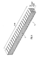
- a known ion guide 1 comprising a stack or plurality of layers of intermediate planar electrodes 2 is shown in Fig. 1 .
- Each layer of intermediate electrodes 2 comprises a first longitudinal electrode and a second longitudinal electrode.
- the longitudinal electrodes in each layer of intermediate planar electrodes 2 are all arranged substantially in the plane in which ions are transmitted in use through the ion guide 1.
- the particular ion guide shown in Fig. 1 comprises four layers of intermediate planar electrodes, a single upper planar electrode 3 and a single lower planar electrode 4.
- the first longitudinal electrode and the second longitudinal electrode are arranged in the same plane and are arranged to have the same phase of a two-phase AC or RF voltage supply 5 applied to them. Opposite phases of a two-phase AC or RF voltage supply 5 are applied to the adjacent or neighbouring vertical layers of intermediate planar electrodes 2.
- the single upper planar electrode 3 and the single lower planar electrode 4 may be supplied with a DC voltage only, an RF voltage only, or a combination of both DC and AC or RF voltages.
- the voltage(s) applied to the single upper planar electrode 3 and the single lower planar electrode 4 act to cause ions to be confined in the vertical radial direction within the ion guide 1,
- the voltage(s) applied to the single upper planar electrode 3 and the single lower planar electrode 4 merely confine ions within the ion guide 1 and do not drive or propel ions through the ion guide 1.
- the AC or RF voltage applied to the longitudinal electrodes in each layer of intermediate planar electrodes 2 generates a pseudo-potential well or barrier which acts to confine ions in the horizontal radial direction within the ion guide 1.
- the geometry of the ion guide 1 provides an ion confining volume between the first and second longitudinal electrodes of each layer of intermediate planar electrodes 2 and between the upper and lower single planar electrodes 3,4. ions can be efficiently transported through the ion confining volume especially when the gas pressure within the ion guide 1 is relatively low. However, if the known ion guide 1 is operated at a relatively high pressure then the kinetic energy of ions passing through the ion guide may be reduced due to collisions between the ions and gas molecules present in the ion guide 1. This will increase the transit time of ions through the known ion guide 1.
- An increased ion transit time may be problematic for certain applications particularly when it is desired to scan or switch a component of a mass spectrometer such as an ion gate, a mass filter or mass analyser or a collision cell arranged downstream of the ion guide 1 relatively quickly.
- a component of a mass spectrometer such as an ion gate, a mass filter or mass analyser or a collision cell arranged downstream of the ion guide 1 relatively quickly.
- the preferred ion guide 7a comprises a plurality or stack of layers of intermediate planar, plate or mesh electrode 2.
- Each layer of intermediate planar, plate or mesh electrodes 2 preferably comprises a first longitudinal electrode and a second longitudinal electrode. According to other embodiments each layer of intermediate planar, plate or mesh electrodes 2 may comprise more than two longitudinal electrodes.
- Each layer of intermediate planar, plate or mesh electrodes 2 are preferably arranged generally or substantially in the plane in which ions are transmitted, in use, through the preferred ion guide 7a.
- the ion guide 7a preferably comprises an array or a plurality of upper electrodes 8a-8e.
- a DC and/or AC or RF voltage is preferably applied to the array or plurality of upper electrodes in order to confine ions within the preferred ion guide 7a and hence to provide an upper boundary or ion confinement region to the preferred ion guide 7a.
- the ion guide 7a preferably comprises an array or a plurality of lower electrodes 9a-9e.
- a DC and/or AC or RF voltage is preferably applied to the array or plurality of lower electrodes in order to confine ions within the preferred ion guide 7a and hence to provide an lower boundary or ion confinement region to the preferred ion guide 7a.
- the first longitudinal electrode and the second longitudinal electrode of each layer of intermediate planar, plate or mesh electrodes 2 are preferably arranged in the same plane and are preferably arranged to have the same phase of a two-phase AC or RF voltage 5 applied to them. Opposite phases of a two-phase AC or RF voltage supply 5 are preferably applied to adjacent vertical or neighbouring layers of intermediate planar, plate or mesh electrodes 2.
- Fig. 2 Each having a first longitudinal electrode and a second longitudinal electrode.
- the preferred ion guide 7a may comprise one, two or three layers of intermediate planar, plate or mesh electrodes.
- the preferred ion guide 7a may comprise 5, 6, 7, 8, 9, 10, 11, 12, 13, 14, 15, 16, 17, 18, 19, 20 or more than 20 separate layers of intermediate planar, plate or mesh electrodes 2.
- the plurality or array of upper electrodes 8a-8e and the plurality or array of lower electrodes 9a-9e may be supplied with either a DC voltage only, or a combination of both DC and AC or RF voltages in order to confine ions within the preferred ion guide 7a.
- the AC or RF voltage which is preferably applied to the layers of intermediate planar, plate or mesh electrodes 2 preferably causes an effective pseudo-potential barrier or potential well to be generated which preferably acts to prevent ions moving towards either of the two longitudinal electrodes which comprise each layer of intermediate planar, plate or mesh electrodes 2. Ions are therefore preferably prevented from moving in a horizontal radial direction towards the first and second longitudinal electrodes of each layer of intermediate planar, plate or mesh electrodes 2. Ions are preferably confined in the vertical radial direction by the DC and/or AC or RF voltage which is preferably applied to the plurality or array of upper electrodes 8a-8e and/or to the plurality or array of lower electrodes 9a-9e.
- the geometry of the preferred ion guide 7a preferably provides an ion guiding volume between the first and second longitudinal electrodes of each of the layers of intermediate planar, plate or mesh electrodes 2 and between the plurality or array of upper electrodes 8a-8e and the plurality or array of lower electrodes 9a-9e. Ions can preferably be efficiently transported along the ion guiding volume and ions are preferably confined radially within the preferred ion guide 7a.
- the preferred ion guide 7a may be maintained at a gas pressure of between 10 -4 -10 mbar or more preferably at a gas pressure between 10 -3 and 1 mbar.
- the plurality of upper electrodes 8a-8e and/or the plurality of lower electrodes 9a-9e preferably comprise or form a set or an array of electrodes which are preferably electrically isolated from one another.
- the plurality of upper electrodes 8a-8g are preferably all arranged in substantially the same plane and the plurality of lower electrodes 9a-9g are preferably all arranged in substantially the same plane.
- some of the upper electrodes 8a-8e may be arranged such that they are not all substantially co-planar.
- some of the plurality of lower electrodes 9a-9e may be arranged so that they are not all substantially co-planar.
- the plurality of upper electrodes 8a-8e and/or the plurality of lower electrodes 9a-9e may be arranged in a mode of operation such that they are maintained in use at substantially the same DC potential or voltage and/or that substantially the same AC or RF voltage is applied to the electrodes.
- opposite phases of a two-phase AC or RF voltage 5 are preferably applied to adjacent layers of intermediate planar, plate or mesh electrodes 2 preferably in a substantially similar manner to the known ion guide 1.
- the ion guide 7a will act in a substantially similar manner to that of the known ion guide 1 as described above with reference to Fig. 1 i.e. ions will not be actively propelled or urged through or along the ion guide 7a.
- the preferred ion guide 7a is operated in a mode of operation wherein one or more transient DC voltages or potentials or one or more transient DC voltage or potential waveforms are additionally applied or are additionally superimposed to the plurality of upper electrodes 8a-8e and to the plurality of lower electrodes 9a-9e.
- one or more axial potential barriers or one or more axial potential wells are created within the ion guiding region of the preferred ion guide 7.
- the ion guiding region is preferably defined by the region below the plurality of upper electrodes 8a-8e, the region between the longitudinal electrodes in the layers of intermediate planar, plate or mesh electrodes 2 and the region above the plurality of lower electrodes 9a-9e.
- the one or more axial potential wells or barriers which are preferably created within the ion guiding region are preferably progressively translated or moved along at least part of the axial length of the preferred ion guide 7a.
- ions are preferably driven, propelled or urged along and through at least a portion of the preferred ion guide 7a.
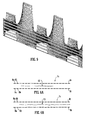
- Fig. 3 illustrates an embodiment of the present invention wherein the preferred ion guide 7b comprises four layers of intermediate planar, plate or mesh electrodes 2.
- the plurality or array of upper electrodes 8a-8g and the plurality or array of lower electrodes 9a-9g each comprise seven separate or discrete electrodes.
- the potential of each electrode in the array of upper and lower electrodes 8a-8g,9a-9g may be independently controllable.
- the number of upper electrodes is preferably the same as the number of lower electrodes.
- the upper electrodes may be arranged differently and/or may have different dimensions to those of the lower electrodes.
- the spacing between the upper electrodes may be different to the spacing between the lower electrodes. It is therefore contemplated that according to less preferred embodiments the number of electrodes in the upper array of electrodes may differ from the number of electrodes in the lower array of electrodes.
- Fig. 3 also shows how according to an embodiment of the present invention one or more transient DC voltages or potentials or one or more transient DC voltage or potential waveforms 10 may be progressively or sequentially applied to the upper electrodes 8a-8g and the lower electrodes 9a-9g of the ion guide 7b.
- Fig. 3 shows how at a first time t 1 a transient DC voltage or potential is preferably applied to the first electrode 8a,9a of the array of upper and lower electrodes 8a-8g,9a-9g.
- a transient DC voltage or potential is preferably then applied to the second electrode 8b,9b of the array of upper and lower electrodes 8a-8g,9a-9g.
- a transient DC voltage or potential is preferably applied to the third electrodes 8c,9c of the array of upper and lower electrodes 8a-8g,9a-9g.
- a transient DC voltage or potential is preferably applied to the fourth 8d,9d, fifth 8e,9e, sixth 8f,9f and seventh 8g,9g electrodes of the array of upper and lower electrodes 8a-8g,9a-9g.
- ions 11 are preferably urged along in front of a travelling potential barrier 10 which is preferably created within the preferred ion guide 7b.
- the ions 11 are therefore preferably propelled or urged along the length of the preferred ion guide 7b ahead of the potential barrier 10 which is preferably translated along the length of the ion guide 7b.
- a moving axial potential barrier or potential well is preferably created which is preferably progressively translated along the length of the preferred ion guide 7a,7b.
- the potential barrier or potential well which is preferably translated along the length of the preferred ion guide 7a,7b preferably causes some or substantially all of the ions 11 to be driven or propelled through the preferred ion guide 7a,7b preferably against background gas which may be present in the preferred ion guide 7a,7b.
- the one or more transient DC voltages or potentials or one or more transient DC voltage or potential waveforms which are applied to the arrays of upper electrodes 8a-Bg and to the lower electrodes 9a-9g preferably has the advantageous effect of reducing the ion transit time through the preferred ion guide 7a,7b.
- a simulation of an ion transiting through a preferred ion guide 7c as shown in Fig. 4 was modelled using the ion optics package SIMION v7.0 (RTM).
- the ion guide 7c was modelled as comprising five layers of intermediate planar electrodes 2.
- Each layer of intermediate planar electrodes 2 comprised a first longitudinal electrode and a second longitudinal electrode.
- Each longitudinal electrode was 0.6 mm thick, 2.4 mm wide and 97 mm long.
- the longitudinal electrodes were modelled as being arranged one above another with a vertical centre-to-centre spacing of 1.6 mm.
- the first and second longitudinal electrodes of each layer were arranged to separated horizontally from one another by 5 mm.
- a two-phase AC or RF voltage was modelled as being applied to the layers of intermediate planar electrodes 2 with both longitudinal electrodes in each layer 2 being connected to the same phase of the AC or RF voltage.
- Vertically adjacent layers of intermediate planar electrodes 2 were arranged to be connected to opposite phases of the AC or RF voltage.
- An array of twenty upper electrodes 8a-8t and an array of twenty lower electrodes 9a-9t was modelled as being provided.
- Each electrode in the array of upper and lower electrodes 8a-8t,9a-9t was modelled as being 0.6 mm thick, 4 mm long (in the axial direction) and 9.8 mm wide.
- the face to face spacing of each electrode in the array of upper electrodes 8a-8t to corresponding electrodes in the array of lower electrodes 9a-9t was modelled as being 9 mm.
- Fig. 5 illustrates a potential surface resulting from applying 10V DC to every third electrode of the array of upper electrodes 8a-8t and by applying 10V DC to every third electrode of the array of lower electrodes 9a-9t.
- a user program was written for the SIMION (RTM) package to enable simulation of collisions between an ion modelled as being present within the ion guide 7c and a neutral gas.
- Fig. 6A shows the trajectory 12 of an ion having an energy of 3eV in an ion guide 7c according to a preferred embodiment but wherein no transient DC voltage or potential was modelled as being applied to either the array of upper electrodes 8a-8t or to the array of lower electrodes 9a-9t.
- An RF voltage having a frequency of 1 MHz and a peak-to-peak amplitude of 200 V was modelled as being applied to the electrodes in the five layers of intermediate planar electrodes 2 in order to confine ions in the horizontal radial direction.
- a constant DC offset of +2 V was simulated as being maintained between the array of upper electrodes 8a-8t and the layers of intermediate planar electrodes 2.
- a constant DC offset of +2V was also simulated as being maintained between the array of lower electrodes 9a-9t relative to layers of intermediate planar electrodes 2.
- the constant DC offset between the array of upper electrodes 8a-8t and the array of lower electrodes 9a-9t relative to the layers of intermediate planar electrodes 2 ensured that ions were confined within the preferred ion guide 7 in the vertical radial direction.
- the gas pressure within the ion guide 7c was simulated as being 1 x 10 -2 mbar. After multiple collisions with the neutral gas molecules the ion was observed to lose axial kinetic velocity to such an extent that the ion did not exit the preferred ion guide 7.
- Fig. 6B shows the trajectory 13 of an ion having an energy of 3eV in a preferred ion guide 7c wherein a transient DC voltage or potential having an amplitude 10 V was modelled as being progressively applied to the electrodes in the arrays of upper and lower electrodes 8a-8t,9a-9t.
- the transient DC voltage or potential was applied to each electrode for a period of 20 ⁇ s before being applied to the next or successive electrode along the length of the ion guide 7c.
- the ion 13 was observed to be efficiently propelled through the preferred ion guide 7c by an axial potential barrier which was preferably progressively translated along the axial length of the preferred ion guide 7c. It is apparent therefore, that from the model the application of a transient DC voltage or potential to the arrays of upper and lower electrodes 8a-8t,9a-9t had the effect of significantly improving the transit time through the preferred ion guide 7c.
- the preferred ion guide has been described as comprising a linear ion guiding region
- the ion transport volume may have a convoluted or substantially curved or irregular path. Such embodiments may be particularly advantageous in certain circumstances.
- the array of upper electrodes and/or the array of lower electrodes may be mounted on one or more printed circuit boards. Such an embodiment has the advantage of simplifying the connections and interconnections of the upper electrodes and the lower electrodes.
- An ion guide 7a,7b,7c may be used to effect the rapid transport of ions through a gas.
- An alternative embodiment of the present invention is contemplated wherein a device substantially similar to the preferred ion guide 7a,7b,7c may be provided but wherein the device may be used as an ion mobility spectrometer or separator.
- the height, amplitude or depth of the one or more DC voltage or potential barriers, hills or wells created within the device may be preferably set to a relatively low level such that at least some ions present within the device will slip or otherwise pass over the potential barrier or hill as it is preferably being translated along the length of the device.
- ions having a relatively high ion mobility will tend to slip over or otherwise pass over the potential barrier or hill as it passes along whereas ions having a relatively low ion mobility will tend to be urged forwards by the potential barrier or hill.
- ions will become temporally separated on the basis of or according to their ion mobility.
- a yet further alternative embodiment of the present invention is contemplated wherein a device substantially similar to the preferred ion guide 7a,7b,7c may be provided but wherein the device may be used as a collision, fragmentation or reaction device.
- ions may be transported through the device or may be transported into the device with sufficient kinetic energy or velocity such that the ions are preferably caused to collide with background gas molecules present in the device thereby causing or otherwise inducing the ions to fragment into fragment or daughter ions.
- the device may accordingly be used as a collision or fragmentation cell preferably as part of a tandem mass spectrometer.
- the tandem mass spectrometer may comprise a quadrupole mass filter, a magnetic sector mass analyser, a linear quadrupole ion trap mass analyser, a 3-D quadrupole ion trap mass analyser, an axial Time of Flight mass analyser, an orthogonal acceleration Time of Flight mass analyser, a Fourier Transform ICR mass analyser, or any combination thereof.
- the device may comprise a collision, reaction or fragmentation device wherein the fragmentation or reaction device is selected from the group consisting of: (i) a Surface Induced Dissociation (“SID”) fragmentation device; (ii) an Electron Transfer Dissociation fragmentation device; (iii) an Electron Capture Dissociation fragmentation device; (iv) an Electron Collision or impact Dissociation fragmentation device; (v) a Photo Induced Dissociation (“PID”) fragmentation device; (vi) a Laser Induced Dissociation fragmentation device; (vii) an infrared radiation induced dissociation device; (viii) an ultraviolet radiation induced dissociation device; (ix) a nozzle-skimmer interface fragmentation device; (x) an in-source fragmentation device; (xi) an ion-source Collision Induced Dissociation fragmentation device; (xii) a thermal or temperature source fragmentation device; (xiii) an electric field induced fragmentation device; (xiv) a
- each layer of intermediate planar, plate or mesh electrodes may comprise more than two longitudinal electrodes.
- each layer of intermediate planar, plate or mesh electrode may comprise 3, 4, 5, 6, 7, 8, 9, 10 or more than 10 longitudinal electrodes.
Abstract
Description
- The present invention relates to a device which may comprise an ion guide, an ion mobility spectrometer or separator or a collision, fragmentation or reaction device. The device preferably forms part of a mass spectrometer. The present Invention also relates to a method of guiding ions, a method of ion mobility spectrometry or ion mobility separation and a method of colliding, fragmenting or reacting ions. The preferred embodiment relates to an ion guide comprising a stack of layers of intermediate planar, plate or mesh electrodes. The ion guide further comprises an array of upper electrodes and an array of lower electrodes. One or more transient DC voltages or potentials or one or more transient DC voltage or potential waveforms are applied to the array of upper electrodes and the array of lower electrodes in order to urge ions along and through at least a portion of the preferred ion guide.
- Multipole rod set ion guides are known comprising four, six or eight parallel rods which are equi-spaced about a circular circumference. The rods are all maintained at substantially the same DC voltage. A two-phase RF voltage is also applied to the rods with adjacent rods being supplied with opposite phases of the RF voltage. The RF voltage applied to the rods causes a symmetrical effective radial pseudo-potential well to be generated within the space circumscribed by the rods. The radial pseudo-potential well causes Ions to be confined radially within the ion guide. The ion guide may be maintained at a relatively high pressure and can result in a reduction in the Ion radial density distribution due to collisional cooling of ions with background gas molecules. The multipole rod set ion guide may be arranged to confine, transport and focus ions in the presence of background gas. The known rod set ion guide may be used, for example, to couple an Atmospheric Pressure ion source to a mass analyser which must be maintained at relatively low pressure.
- Another form of ion guide is known which comprises a plurality or stack of ring electrodes having apertures through which ions are transmitted in use. Opposite phases of a two-phase AC or RF voltage are applied to adjacent electrodes. The ion guide may comprise an ion tunnel ion guide comprising electrodes which have apertures which are all substantially the same size or diameter. Alternatively, the ion guide may comprise an ion funnel ion guide comprising a plurality of electrodes which have apertures which progressively decrease in diameter along the axial length of the ion guide.
- Another form of Ion guide is known which comprises a stack or a plurality of layers of intermediate planar electrodes. Such an ion guide is shown In
GB-2392005 - The known ion guide comprising a stack of layers of intermediate planar electrodes and single upper and lower planar electrodes is particularly advantageous compared to other known ion guides in that various complex and efficient ion transport volumes or geometries can be provided that would be otherwise be very difficult to provide using a rod set ion guide or an ion guide comprising a plurality of ring electrodes.
- Ion guides comprising a stack or plurality of layers of intermediate planar electrodes can be relatively easily designed so as to transport ions along relatively convoluted or potentially complex ion paths. A further advantage of an ion guide comprising a plurality of layers of intermediate planar electrodes is that the shape and/or area of the ion confinement volume can be arranged to vary along the length of the ion guide. This enables the ion guide to effectively couple two components of a mass spectrometer which may have different ion-optical acceptance profiles.
- According to an arrangement an ion guide comprising a plurality of layers of intermediate planar electrodes may be arranged so that two or more separate ion guides merge into a single ion guide. Alternatively, according to another arrangement an ion guide comprising a plurality of layers of intermediate planar electrodes may be arranged so that an ion guide divides into two or more separate ion guides.
- The known ion guide comprising a plurality of layers of intermediate planar electrodes and single upper and lower planar electrodes suffers from the problem that collisions between ions and background gas molecules present within the ion guide may reduce the kinetic energy of the ions as they pass through the ion guide. This can have the effect of increasing the transit times of ions as they pass through the ion guide.
- According to an aspect of the present invention there is provided a device as claimed in claim 1.
- The first array of first electrodes preferably comprises at least 2, 3, 4, 5, 6, 7, 8. 9, 10, 11, 12, 13, 14, 15, 16, 17, 18, 19, 20 or more than 20 electrodes.
- The first array of first electrodes may comprise: (i) a printed circuit board, printed wiring board or etched wiring board; (ii) a plurality of conductive traces applied or laminated onto a non-conductive substrate; (iii) a plurality of copper or metallic electrodes arranged on a substrate; (iv) a screen printed, photoengraved, etched or milled printed circuit board; (v) a plurality of electrodes arranged on a paper substrate impregnated with phenolic resin; (vi) a plurality of electrodes arranged on a fibreglass mat impregnated within an epoxy resin; (vii) a plurality of electrodes arranged on a plastic substrate; or (viii) a plurality of electrodes arranged on a substrate.
- According to an embodiment at least 5%. 10%, 15%, 20%, 25%, 30%, 35%, 40%, 45%, 50%, 55%, 60%, 65%, 70%, 75%, 80%, 85%, 90%, 95% or 100% of the first electrodes have an axial centre to centre spacing selected from the group consisting of: (i) < 1 mm; (ii) 1-2 mm; (iii) 2-3 mm; (Iv) 3-4 mm; (v) 4-5 mm; (vi) 5-6 mm; (vii) 6-7 mm; (viii) 7-8 mm; (Ix) 8-9 mm; (x) 9-10 mm; (xi) 10-11 mm; (xii) 11-12 mm; (xiii) 12-13 mm; (xiv) 13-14 mm; (xv) 14-15 mm; (xvi) 15-16 mm; (xvii) 16-17 mm; (xviii) 17-18 mm; (xix) 18-19 mm; (xx) 19-20 mm; and (xxi) > 20 mm.
- At least 5%, 10%, 15%, 20%, 25%, 30%. 35%, 40%, 45%, 50%, 55%, 60%, 65%, 70%, 75%, 80%, 85%, 90%, 95% or 100% of the first electrodes preferably have an axial length selected from the group consisting of: (i) < 1 mm; (ii) 1-2 mm; (iii) 2-3 mm; (iv) 3-4 mm; (v) 4-5 mm; (vi) 5-6 mm; (vii) 6-7 mm; (viii) 7-8 mm; (ix) 8-9 mm; (x) 9-10 mm; (xi) 10-11 mm; (xii) 11-12 mm; (xiii) 12-13 mm; (xiv) 13-14 mm; (xv) 14-15 mm; (xvi) 15-16 mm; (xvii) 16-17 mm; (xviii) 17-18 mm; (xix) 18-19 mm; (xx) 19-20 mm; and (xxi) > 20 mm.
- According to an embodiment at least 5%, 10%, 15%, 20%, 25%, 30%. 35%, 40%, 45%, 50%, 55%, 60%, 65%, 70%, 75%, 80%, 85%, 90%, 95% or 100% of the first electrodes have a width selected from the group consisting of: (i) < 1 mm; (ii) 1-2 mm; (iii) 2-3 mm; (iv) 3-4 mm; (v) 4-5 mm; (vi) 5-6 mm; (vii) 6-7 mm; (viii) 7-8 mm; (ix) 8-9 mm; (x) 9-10 mm; (xi) 10-11 mm; (xii) 11-12 mm; (xiii) 12-13 mm; (xiv) 13-14 mm; (xv) 14-15 mm; (xvi) 15-16 mm; (xvii) 16-17 mm; (xviii) 17-18 mm; (xix) 18-19 mm; (xx) 19-20 mm; and (xxi) > 20 mm.
- The first electrodes preferably have a thickness selected from the group consisting of: (i) < 0.01 mm; (ii) 0.01-0.1 mm; (iii) 0.1-0.2 mm; (iv) 0.2-0.3 mm; (v) 0.3-0.4 mm; (vi) 0.4-0.5 mm; (vii) 0.5-0.6 mm; (viii) 0.6-0.7 mm; (ix) 0.7-0.8 mm; (x) 0.8-0.9 mm: (xi) 0.9-1.0 mm; (xii) 1-2 mm; (xiii) 2-3 mm; (xiv) 3-4 mm; (xv) 4-5 mm; and (xvi) > 5 mm.
- At least 5%, 10%, 15%, 20%, 25%, 30%, 35%, 40%, 45%, 50%, 55%. 60%, 65%, 10%; 75%, 80%; 85%, 90%, 95% or 100% of the first electrodes are preferably biased, in use, at a first bias DC voltage or potential with respect to the mean or average voltage or potential of at least some or all of the intermediate planar, plate or mesh electrodes. The first DC bias voltage or potential is preferably selected from the group consisting of: (i) less than -10V; (ii) -9 to -8V; (iii) -8 to -7V; (iv) -7 to -6V; (v) -6 to -5V; (vi) -5 to -4V; (vii) -4 to -3V; (viii) -3 to -2V; (ix) -2 to -1V; (x) -1 to 0V; (xi) 0 to 1V; (xii) 1 to 2V; (xiii) 2 to 3V; (xiv) 3 to 4V; (xv) 4 to 5V; (xvi) 5 to 6V; (xvii) 6 to 7V; (xviii) 7 to 8V; (xix) 8 to 9V; (xx) 9 to 10V; and (xxi) more than 10V.
- According to an embodiment the first array of first electrodes are preferably supplied in a mode of operation with a DC only voltage. According to another embodiment, the first array of first electrodes may be supplied in a mode of operation with a DC and an AC or RF voltage.
- The voltage means is arranged and adapted to apply one or more transient DC voltages or potentials or one or more transient DC voltage or potential waveforms to the first array of first electrodes in order to urge, propel, force or accelerate at least some ions through and/or along at least a portion or at least 5%, 10%, 15%, 20%, 25%, 30%. 35%, 40%. 45%, 50%, 55%. 60%, 65%, 70%, 75%, 80%, 85%, 90%, 95% or 100% of the device.
- The second array of second electrodes comprises at least 2, 3, 4, 5, 6, 7, 8, 9, 10, 11, 12, 13, 14, 15, 16, 17, 18, 19, 20 or more than 20 electrodes.
- The second array of second electrodes may comprise: (i) a printed circuit board, printed wiring board or etched wiring board; (ii) a plurality of conductive traces applied or laminated onto a non-conductive substrate; (iii) a plurality of copper or metallic electrodes arranged on a substrate: (iv) a screen printed, photoengraved, etched or milled printed circuit board; (v) a plurality of electrodes arranged on a paper substrate impregnated with phenolic resin; (vi) a plurality of electrodes arranged on a fibreglass mat impregnated within an epoxy resin; (vii) a plurality of electrodes arranged on a plastic substrate; or (viii) a plurality of electrodes arranged on a substrate.
- At least 5%, 10%, 15%, 20%, 25%, 30%, 35%, 40%, 45%, 50%, 55%, 60%, 65%, 70%, 75%, 80%, 85%, 90%, 95% or 100% of the second electrodes preferably have an axial centre to centre spacing selected from the group consisting of: (i) < 1 mm; (ii) 1-2 mm; (iii) 2-3 mm; (iv) 3-4 mm; (v) 4-5 mm; (vi) 5-6 mm; (vii) 6-7 mm; (viii) 7-8 mm; (ix) 8-9 mm; (x) 9-10 mm; (xi) 10-11 mm; (xii) 11-12 mm; (xiii) 12-13 mm; (xiv) 13-14 mm; (xv) 14-15 mm; (xvi) 15-16 mm; (xvii) 16-17 mm; (xviii) 17-18 mm; (xix) 18-19 mm; (xx) 19-20 mm; and (xxi) > 20 mm.
- At least 5%, 10%, 15%, 20%, 25%, 30%, 35%, 40%, 45%, 50%, 55%, 60%, 65%, 70%, 75%, 80%, 85%. 90%, 95% or 100% of the second electrodes preferably have an axial length selected from the group consisting of: (i) < 1 mm; (ii) 1-2 mm; (iii) 2-3 mm; (iv) 3-4 mm; (v) 4-5 mm; (vi) 5-6 mm; (vii) 6-7 mm; (viii) 7-8 mm; (ix) 8-9 mm; (x) 9-10 mm; (xi) 10-11 mm; (xii) 11-12 mm; (xiii) 12-13 mm; (xiv) 13-14 mm; (xv) 14-15 mm; (xvi) 15-16 mm; (xvii) 16-17 mm; (xviii) 17-18 mm; (xix) 18-19 mm; (xx) 19-20 mm; and (xxi) > 20 mm.
- According to an embodiment at least 5%, 10%, 15%. 20%, 25%, 30%, 35%, 40%, 45%, 50%, 55%, 60%, 65%, 70%, 75%, 80%, 85%, 90%, 95% or 100% of the second electrodes have a width selected from the group consisting of: (i) < 1 mm; (ii) 1-2 mm; (iii) 2-3 mm; (iv) 3-4 mm; (v) 4-5 mm: (vi) 5-6 mm; (vii) 6-7 mm; (viii) 7-8 mm; (ix) 8-9 mm; (x) 9-10 mm; (xi) 10-11 mm; (xii) 11-12 mm; (xiii) 12-13 mm; (xiv) 13-14 mm; (xv) 14-15 mm; (xvi) 15-16 mm; (xvii) 16-17 mm; (xviii) 17-18 mm; (xix) 18-19 mm; (xx) 19-20 mm; and (xxi) > 20 mm.
- The second electrodes preferably have a thickness selected from the group consisting of: (i) < 0.01 mm; (ii) 0.01-0.1 mm; (iii) 0.1-0-2 mm; (iv) 0.2-0.3 mm; (v) 0.3-0.4 mm; (vi) 0.4-0.5 mm; (vii) 0.5-0.6 mm; (viii) 0.6-0.7 mm; (ix) 0.7-0.8 mm; (x) 0.8-0.9 mm; (xi) 0.9-1.0 mm; (xii) 1-2 mm; (xiii) 2-3 mm; (xiv) 3-4 mm; (xv) 4-5 mm; and (xvi) > 5 mm.
- At least 5%, 10%, 15%, 20%, 25%, 30%, 35%, 40%, 45%, 50%, 55%, 60%, 65%, 70%, 75%, 80%, 85%, 90%, 95% or 100% of the second electrodes are preferably biased, in use, at a second bias DC voltage or potential with respect to the mean or average voltage or potential of at least some or all of the planar, plate or mesh electrodes. The second DC bias voltage or potential is preferably selected from the group consisting of: (i) less than -10V; (ii) -9 to -8V; (iii) -8 to -7V; (iv) -7 to - 6V; (v) -6 to -5V; (vi) -5 to -4V; (vii) -4 to -3V; (viii) -3 to -2V; (ix) -2 to -1V; (x) -1 to 0V; (xi) 0 to 1 V; (xii) 1 to 2V; (xiii) 2 to 3V; (xiv) 3 to 4V; (xv) 4 to 5V; (xvi) 5 to 6V; (xvii) 6 to 7V; (xviii) 7 to 8V; (xix) 8 to 9V; (xx) 9 to 10V; and (xxi) more than 10V.
- According to an embodiment the second array of second electrodes are supplied in a mode of operation with a DC only voltage. According to another embodiment the second array of second electrodes may be supplied in a mode of operation with a DC and an AC or RF voltage.
- The voltage means is arranged and adapted to apply one or more transient DC voltages or potentials or one or more transient DC voltage or potential waveforms to the second array of second electrodes in order to urge, propel, force or accelerate at least some ions through and/or along at least a portion or at least 5%, 10%, 15%, 20%, 25%, 30%, 35%, 40%, 45%, 50%, 55%, 60%, 65%, 70%, 75%, 80%, 85%, 90%, 95% or 100% of the device.
- According to an embodiment of the present invention, the device may comprise means for maintaining a non-zero DC voltage or potential gradient along at least a portion or at least 5%. 10%, 15%, 20%, 25%, 30%, 35%, 40%, 45%, 50%, 55%, 60%, 65%, 70%, 75%, 80%, 85%, 90%, 95% or 100% of the axial length of the device.
- The non-zero DC voltage or potential gradient may cause ions to be accelerated along at least a portion or at least 5%, 10%, 15%, 20%, 25%, 30%, 35%, 40%, 45%, 50%, 55%, 60%, 65%, 70%, 75%, 80%, 85%, 90%, 95% or 100% of the axial length of the device.
- Alternatively, the non-zero DC voltage or potential gradient may present a potential barrier or hill which acts to oppose the onward transmission of ions or which acts to decelerate ions. The non-zero DC voltage or potential gradient being maintained along at least a portion or at least 5%, 10%, 15%, 20%, 25%, 30%, 35%, 40%, 45%, 50%, 65%, 60%, 65%, 70%, 75%, 80%, 85%, 90%, 95% or 100% of the axial length of the device. According to an embodiment the non-zero DC voltage or potential gradient which opposes the onward transmission of ions may be maintained across a relatively short distance e.g. < 5% of the axial length of the device. It is contemplated that the non-zero DC voltage or potential gradient which opposes the onward transmission of ions may be maintained only across < 4%, < 3%, < 2% or < 1% of the axial length of the device.
- According to a preferred aspect of the present invention the voltage means may be arranged to cause ions to overcome the effects of the non-zero DC voltage or potential gradient so that at least a portion or at least 5%, 10%, 15%, 20%, 25%, 30%, 35%, 40%, 45%, 50%, 55%, 60%, 65%, 70%, 75%, 80%, 85%, 90%, 95% or 100% of ions within the device are onwardly transmitted across or through the non-zero DC voltage or potential gradient. For example, a potential barrier may be maintained across a portion of the device which opposes the onward transmission of ions and one or more transient DC voltages or potentials or one or more transient DC voltage or potential waveforms may be applied to the upper and lower electrodes in order to urge, force, propel, or accelerate ions to overcome the potential barrier and hence to be onwardly transmitted.
- According to an embodiment the one or more layers of intermediate planar, plate or mesh electrodes may comprise 1, 2, 3, 4, 5, 6, 7, 8, 9, 10, 11, 12, 13, 14, 15, 16, 17, 18, 19, 20 or more than 20 layers of intermediate planar, plate or mesh electrodes. Each layer of intermediate planar, plate or mesh electrodes preferably comprises two or more longitudinal electrodes.
- According to an embodiment at least one or at least two of the longitudinal electrodes preferably have a centre to centre separation in a width direction selected from the group consisting of: (i) < 1 mm; (ii) 1-2 mm; (iii) 2-3 mm; (iv) 3-4 mm; (v) 4-5 mm; (vi) 5-6 mm; (vii) 6-7 mm; (viii) 7-8 mm; (ix) 8-9 mm; (x) 9-10 mm; (xi) 10-11 mm; (xii) 11-12 mm; (xiii) 12-13 mm; (xiv) 13-14 mm; (xv) 14-15 mm; (xvi) 15-16 mm; (xvii) 16-17 mm; (xviii) 17-18 mm; (xix) 18-19 mm; (xx) 19-20 mm; and (xxi) > 20 mm. Preferably, at least one or at least two of the longitudinal electrodes have an axial length selected from the group consisting of: (i) < 10 mm; (ii) 10-20 mm; (iii) 20-30 mm; (iv) 30-40 mm; (v) 40-50 mm; (vi) 50-60 mm; (vii) 60-70 mm; (viii) 70-80 mm; (ix) 80-90 mm; (x) 90-100 mm; (xi) 100-110 mm; (xii) 110-120 mm; (xiii) 120-130 mm; (xiv) 130-140 mm; (xv) 140-150 mm; (xvi) 150-160 mm; (xvii) 160-170 mm; (xviii) 170-180 mm; (xix) 180-190 mm; (xx) 190-200 mm; and (xxi) > 200 mm.
- According to an embodiment at least one or at least two of the longitudinal electrodes have a width selected from the group consisting of: (i) < 1 mm; (il) 1-2 mm; (iii) 2-3 mm; (iv) 3-4 mm; (v) 4-5 mm; (vi) 5-6 mm; (vii) 6-7 mm; (viii) 7-8 mm; (ix) 8-9 mm; (x) 9-10 mm; (xi) 10-11 mm; (xii) 11-12 mm; (xiii) 12-13 mm; (xiv) 13-14 mm; (xv) 14-15 mm; (xvi) 15-16 mm; (xvii) 16-17 mm; (xviii) 17-18 mm; (xix) 18-19 mm; (xx) 19-20 mm; and (xxi) > 20 mm. Preferably, at least one or at least two of the longitudinal electrodes have a thickness selected from the group consisting of: (i) < 0.01 mm; (ii) 0.01-0.1 mm; (iii) 0.1-0.2 mm; (iv) 0.2-0.3 mm; (v) 0.3-0.4 mm; (vi) 0.4-0.5 mm; (vii) 0.5-0.6 mm: (viii) 0.6-0.7 mm; (ix) 0.7-0.8 mm; (x) 0.8-0.9 mm; (xi) 0.9-1.0 mm; (xii) 1-2 mm; (xiii) 2-3 mm; (xiv) 3-4 mm; (xv) 4-5 mm; and (xvi) > 5 mm.
- The two or more longitudinal electrodes are preferably substantially co-planar.
- According to the preferred embodiment the two or more longitudinal electrodes in a layer of intermediate planar, plate or mesh electrodes are supplied, in use, with substantially the same phase of a two-phase or multi-phase AC or RF voltage or signal. Adjacent layers of planar, plate or mesh electrodes in the vertical direction are preferably supplied with opposite or different phases of the AC or RF voltage or signal. The AC or RF voltage or signal preferably has a frequency selected from the group consisting of: (i) < 100 kHz; (ii) 100-200 kHz; (iii) 200-300 kHz; (iv) 300-400 kHz; (v) 400-500 kHz; (vi) 0.5-1.0 MHz; (vii) 1.0-1.5 MHz; (viii) 1.5-2.0 MHz; (ix) 2.0-2.5 MHz; (x) 2.5-3.0 MHz; (xi) 3.0-3.5 MHz; (xii) 3.5-4.0 MHz; (xiii) 4.0-4.5 MHz; (xiv) 4.5-5.0 MHz; (xv) 5.0-5.5 MHz; (xvi) 5.5-6.0 MHz; (xvii) 6.0-6.5 MHz; (xviii) 6.5-7.0 MHz; (xix) 7.0-7.5 MHz; (xx) 7.5-8.0 MHz; (xxi) 8.0-8.5 MHz; (xxii) 8.5-9.0 MHz; (xxiii) 9.0-9.5 MHz; (xxiv) 9.5-10.0 MHz; and (xxv) > 10.0 MHz. The amplitude of the AC or RF voltage or signal is preferably selected from the group consisting of: (i) < 50V peak to peak: (ii) 50-100V peak to peak; (iii) 100-150V peak to peak; (iv) 150-200V peak to peak; (v) 200-250V peak to peak; (vi) 250-300V peak to peak: (vii) 300-350V peak to peak; (viii) 350-400V peak to peak; (ix) 400-450V peak to peak; (x) 450-500V peak to peak; and (xi) > 500V peak to peak.
- According to an embodiment at least 5%, 10%, 15%, 20%, 25%, 30%, 35%, 40%, 45%, 50%, 55%, 60%, 65%, 70%, 75%, 80%, 85%, 90%, 95°5% or 100% of the intermediate planar, plate or mesh electrodes are supplied with an AC or RF voltage or signal. At least 5%, 10%, 15%, 20%, 25%, 30%, 35%, 40%, 45%, 50%, 55%, 60%, 65%, 70%, 75%, 80%, 85%, 90%, 95% or 100% of the layers of intermediate planar, plate or mesh electrodes are preferably arranged substantially parallel to one another.
- According to an embodiment at least 5%, 10%, 16%, 20%, 25%, 30%, 35%, 40%, 45%, 50%, 55%, 60%, 65%, 70%, 75%, 80%, 85%. 90%, 95% or 100% of the layers of intermediate planar, plate or mesh electrodes are substantially planar or flat and the device curves in the plane of the electrodes.
- According to another embodiment at least 5%, 10%, 15%, 20%, 25%, 30%, 35%, 40%, 45%. 50%, 55%, 60%, 65%, 70%, 75%, 80%, 85%, 90%, 95% or 100% of the layers of intermediate planar, plate or mesh electrodes are substantially nonplanar or non-flat such that the electrodes curve upwards or downwards along their axial length. It is contemplated that the electrodes may curve in some other manner.
- At least 5%, 10%, 15%, 20%, 25%, 30%, 35%, 40%, 45%, 50%, 55%, 60%, 65%, 70%, 75%, 80%, 85%, 90%, 95% or 100% of the layers of Intermediate planar, plate or mesh electrodes are preferably arranged substantially equidistant from one another.
- At least 5%, 10%, 16%, 20%, 25%, 30%, 35%, 40%, 45%, 50%, 55%, 60%, 65%, 70%, 75%, 80%, 85%, 90%, 95% or 100% of the layers of intermediate planar, plate or mesh electrodes are preferably spaced apart from one another by a distance selected from the group consisting of: (i) less than or equal to 5 mm; (ii) less than or equal to 4.5 mm; (iii) less than or equal to 4 mm; (iv) less than or equal to 3.5 mm; (v) less than or equal to 3 mm; (vi) less than or equal to 2.5 mm; (vii) less than or equal to 2 mm; (viii) less than or equal to 1.5 mm; (ix) less than or equal to 1 mm; (x) less than or equal to 0.8 mm; (xi) less than or equal to 0.6 mm; (xii) less than or equal to 0.4 mm; (xiii) less than or equal to 0.2 mm; (xiv) less than or equal to 0.1 mm; and (xv) less than or equal to 0.25 mm.
- According to the preferred embodiment the device preferably has a substantially linear ion guiding region. According to an alternative embodiment the device may have a substantially curved ion guiding region.
- The device may have an entrance for receiving ions along a first axis and an exit from which ions emerge from the device along a second axis, wherein the second axis makes an angle θ to the first axis, and wherein θ falls within a range selected from the group consisting of: (i) < 10°; (ii) 10-20°; (iii) 20-30°; (iv) 30-40°; (v) 40-50°; (vi) 50-60°; (vii) 60-70°; (viii) 70-80°; (ix) 80-90°; (x) 90-100°; (xi) 100-110°; (xii) 110-120°; (xiii) 120-130°; (xiv) 130-140°; (xv) 140-150°; (xvi) 150-160°; (xvii) 160-170°; and (xviii) 170-180°.
- The device may comprise an ion guiding region arranged between an ion entrance of the device and an ion exit of the device, and wherein the ion guiding region is substantially linear, curved, "S"-shaped or has one or more points of inflexion.
- The device may have one or more separate entrances for receiving ions and one or more separate exits from which ions may emerge from the device. According to a preferred embodiment the device may comprise a Y-shaped arrangement wherein two separate ion guides merge into a single ion guide or alternatively a single ion guide diverges into two separate ion guides. According to another embodiment the device may comprise an X-shaped arrangement wherein two separate ion guides cross over to form two separate ion guides.
- According to a preferred embodiment the device may have an entrance having a first cross-sectional profile and a first cross-sectional area and an exit having a second cross-sectional profile and a second cross-sectional area. The first cross-sectional profile may be different to the second cross-sectional profile and/or the first cross-sectional area may be different to the second cross-sectional area. The first cross-sectional profile and/or the second cross-sectional profile may have a substantially circular, oval, rectangular or square cross-section.
- The device may be arranged and adapted to be coupled to an ion-optical component selected from the group consisting of: (I) an ion-optical component having a substantially circular, square, rectangular or elliptical cross-sectional profile; (ii) a quadrupole mass filter/analyser having a substantially circular or elliptical cross-sectional profile; (iii) an orthogonal acceleration Time of Flight mass analyser having a substantially square or rectangular cross-sectional profile; (iv) a magnetic sector analyser having a substantially rectangular cross-sectional profile; (v) a Fourier Transform Ion Cyclotron Resonance ("FTICR") mass analyser having a substantially circular or elliptical cross-sectional profile; (vi) a 2D (linear) quadrupole ion trap having a substantially circular or elliptical cross-sectional profile; and (vii) a 3D (Paul) quadrupole ion trap having a substantially circular or elliptical cross-sectional profile.
- The device may comprise an ion guiding region arranged between an entrance and an exit, and wherein the ion guiding region either: (i) varies in size and/or shape along the length of the ion guiding region; or (ii) has a width and/or height which progressively tapers or enlarges in size.
- The device may be maintained, in use, at a pressure selected from the group consisting of: (i) > 0.0001 mbar; (ii) > 0.001 mbar; (iii) > 0.01 mbar; (iv) > 0.1 mbar; (v) > 1 mbar; (vi) > 10 mbar; (vii) > 100 mbar: (viii) 0.0001-0.001 mbar; (ix) 0.001-0.01 mbar: (x) 0.01-0.1 mbar; (xi) 0.1-1 mar: (xii) 1-10 mbar; (xiii) 10-100 mbar; and (xiv) 100-1000 mbar.
- The device may be maintained, in use, at a pressure selected from the group consisting of: (i) < 0.0001 mbar; (ii) < 0.001 mbar; (iii) < 0.01 mbar; (iv) < 0.1 mbar; (v) < 1 mbar; (vi) < 10 mbar; (vii) > 100 mbar; (viii) 0.0001-100 mbar; (ix) 0.001-10 mbar, and (x) 0.01-1 mbar.
- According to the preferred embodiment the device preferably comprises an ion guide.
- According to an alternative embodiment the device may comprise an ion mobility spectrometer or separator, preferably a gas phase electrophoresis device.
- The one or more transient DC voltages or potentials or one or more transient DC voltage or potential waveforms applied to the upper and lower electrodes may have a relatively low amplitude. As a result, ions having a relatively high ion mobility may slip or pass over the relatively low amplitude potential hill as it is translated along the length of the device. However, ions having a relatively low ion mobility may be urged along the device by the relatively low amplitude potential hill. Ions are therefore preferably temporally separated according to their ion mobility.
- It is also contemplated that a device substantially similar to the preferred ion guide may be provided wherein ions are separated according to another physico-chemical property other than ion mobility. For example, ions may be separated according to their mass to charge ratio or on the basis of their rate of change of ion mobility with electric field strength. It is contemplated therefore that a Field Asymmetric Ion Mobility Spectrometry or "FAIMS" device may also be provided having the same structure as the preferred ion guide.
- According to another embodiment the device may comprise a collision, fragmentation or reaction device. The device may be arranged and adapted to fragment ions by Collision Induced Dissociation ("CID"). According to this embodiment, ions may be accelerated such that they have a relatively high kinetic energy when they enter the device that they are caused to fragment into fragment or daughter ions upon colliding with gas molecules in the device. Alternatively and/or additionally, ions may accelerated within the device such that they collide energetically with background gas molecules within the device and fragment into fragment or daughter ions.
- Alternatively, the collision, fragmentation or reaction device may selected from the group consisting of: (i) a Surface Induced Dissociation ("SID") fragmentation device; (ii) an Electron Transfer Dissociation fragmentation device; (iii) an Electron Capture Dissociation fragmentation device; (iv) an Electron Collision or Impact Dissociation fragmentation device; (v) a Photo Induced Dissociation ("PID") fragmentation device: (vi) a Laser induced Dissociation fragmentation device; (vii) an infrared radiation induced dissociation device; (viii) an ultraviolet radiation induced dissociation device; (ix) a nozzle-skimmer interface fragmentation device; (x) an in-source fragmentation device; (xi) an ion-source Collision Induced Dissociation fragmentation device; (xii) a thermal or temperature source fragmentation device: (xiii) an electric field induced fragmentation device; (xiv) a magnetic field induced fragmentation device; (xv) an enzyme digestion or enzyme degradation fragmentation device; (xvi) an ion-ion reaction fragmentation device; (xvii) an ion-molecule reaction fragmentation device; (xviii) an ion-atom reaction fragmentation device; (xix) an ion-metastable ion reaction fragmentation device: (xx) an ion-metastable molecule reaction fragmentation device; (xxi) an ion-metastable atom reaction fragmentation device; (xxii) an ion-ion reaction device for reacting ions to form adduct or product ions; (xxiii) an ion-molecule reaction device for reacting ions to form adduct or product ions; (xxiv) an ion-atom reaction device for reacting ions to form adduct or product ions: (xxv) an ion-metastable ion reaction device for reacting ions to form adduct or product ions; (xxvi) an ion-metastable molecule reaction device for reacting ions to form adduct or product ions; and (xxvii) an ion-metastable atom reaction device for reacting ions to form adduct or product ions.
- A reaction device should be understood as comprising a device wherein ions, atoms or molecules are rearranged or reacted so as to form a new species of ion, atom or molecule. An X-Y reaction fragmentation device should be understood as meaning a device wherein X and Y combine to form a product which then fragments. This is different to a fragmentation device per se wherein ions may be caused to fragment without first forming a product. An X-Y reaction device should be understood as meaning a device wherein X and Y combine to form a product and wherein the product does not necessarily then fragment.
- A plurality of insulator layers may be interspersed or interleaved between the one or more layers of intermediate planar, plate or mesh electrodes and optionally also between the intermediate planar, plate or mesh electrodes and the upper and/or lower array of electrodes.
- At least 5%, 10%, 15%, 20%, 25%. 30%, 35%, 40%, 45%, 50%, 55%, 60%, 65%, 70%, 75%, 80%, 85%, 90%, 95% or 100% of the one or more layers of intermediate planar, plate or mesh electrodes may be arranged on or are deposited on the insulator layers.
- According to an embodiment in a mode of operation the device is arranged and adapted to transmit ions in a first axial direction. In another mode of operation the device may be arranged and adapted to transmit ions in a second axial direction, wherein the second axial direction forms an angle α to the first axial direction, and wherein α is selected from the group consisting of: (i) < 10°; (ii) 10-20°; (iii) 20-30°; (iv) 30-40°; (v) 40-50°; (vi) 50-60°; (vii) 60-70°; (viii) 70-80°; (ix) 80-90°; (x) 90-100°; (xi) 100-110°; (xii) 110-120°; (xiii) 120-130°; (xiv) 130-140°; (xv) 140-150°; (xvi) 150-160°; (xvii) 160-170°; (xviii) 170-180°; and (xix) substantially 180°.
- A preferred aspect of the device is that it may be arranged and adapted to receive a substantially continuous beam of ions and the device may release or eject ions as a plurality of packets or bunches of ions. The device or ion guide may be arranged and adapted to convert a substantially continuous beam of ions into a pulsed or discontinuous beam of ions.
- According to another aspect of the present invention there is provided a mass spectrometer comprising one or more devices as described above. The mass spectrometer preferably further comprises an ion source. The ion source may be selected from the group consisting of: (i) an Electrospray ionisation ("ESI") ion source; (ii) an Atmospheric Pressure Photo Ionisation ("APPI") ion source; (ill) an Atmospheric Pressure Chemical Ionisation ("APCI") ion source; (iv) a Matrix Assisted Laser Desorption Ionisation ("MALDI") ion source: (v) a Laser Desorption Ionisation ("LDI") ion source; (vi) an Atmospheric Pressure Ionisation ("API") ion source; (vii) a Desorption Ionisation on Silicon ("DIOS") ion source; (viii) an Electron Impact ("EI") ion source; (ix) a Chemical Ionisation ("CI") ion source; (x) a Field Ionisation ("FI") ion source; (xi) a Field Desorption ("FD") ion source; (xii) an Inductively Coupled Plasma ("ICP") ion source: (xiii) a Fast Atom Bombardment ("FAB") ion source; (xiv) a Liquid Secondary Ion Mass Spectrometry ("LSIMS") ion source; (xv) a Desorption Electrospray lonisation ("DESI") ion source; (xvi) a Nickel-63 radioactive ion source; (xvii) an Atmospheric Pressure Matrix Assisted Laser Desorption Ionisation ion source; and (xviii) a Thermospray ion source.
- The ion source may comprise a pulsed or continuous ion source.
- A mass analyser is preferably arranged downstream of the device. The mass analyser may be selected from the group consisting of: (i) a quadrupole mass analyser; (ii) a 2D or linear quadrupole mass analyser: (iii) a Paul or 3D quadrupole mass analyser; (iv) a Penning trap mass analyser; (v) an ion trap mass analyser; (vi) a magnetic sector mass analyser; (vii) Ion Cyclotron Resonance ("ICR") mass analyser; (viii) a Fourier Transform Ion Cyclotron Resonance ("FTICR") mass analyser: (ix) an electrostatic or orbitrap mass analyser; (x) a Fourier Transform electrostatic or orbitrap mass analyser; (xi) a Fourier Transform mass analyser; (xii) a Time of Flight mass analyser; (xiii) an axial acceleration Time of Flight mass analyser; and (xiv) an orthogonal acceleration Time of Flight mass analyser.
- The mass spectrometer may further comprise one or more mass or mass to charge ratio filters and/or mass analysers arranged upstream and/or downstream of the device. The one or more mass or mass to charge ratio filters and/or analysers may be selected from the group consisting of: (i) a quadrupole mass filter or analyser; (ii) a Wien filter; (iii) a magnetic sector mass filter or analyser; (iv) a velocity filter; and (v) an ion gate.
- According to an aspect of the present invention there is provided a method of guiding ions as claimed in claim 26.
- The method preferably further comprises passing or guiding ions though or along the device.
- According to another aspect of the present invention there is provided a method of ion mobility spectrometry or ion mobility separation as claimed in claim 27.
- The method preferably further comprises passing or transmitting ions into the device and allowing the ions to become temporally separated on the basis of their mass, mass to charge ratio or other physico-chemical property.
- According to another aspect of the present invention there is provided a method of colliding, fragmenting or reacting ions as claimed in claim 28.
- The method preferably further comprises passing or transmitting ions into the device and allowing or arranging for the ions collide, fragment or react preferably with gas molecules present in the device.
- According to another aspect of the present invention there is provided a method of mass spectrometry comprising one or more of the methods as discussed above.
- The preferred embodiment relates to an ion guide comprising a plurality of intermediate plate, planar or mesh electrodes and a plurality or array of upper electrodes and a plurality or array of lower electrodes. One or more transient DC voltages or potentials or one or more transient DC voltage or potential waveforms are preferably applied to the upper and lower electrodes so as to urge, propel, force or accelerate ions along and through the preferred ion guide.
- The preferred embodiment enables a plurality of complex ion guide geometries or designs to be provided and enables the motion of ions through the ion guide to be effectively controlled. The transit times of ions through an ion guide according to the preferred embodiment may be significantly improved compared with conventional ion guides.
- Various embodiments of the present invention together with an arrangement given for illustrative purposes only will now be described, by way of example only, and with reference to the accompanying drawings in which:
-
Fig. 1 shows a known ion guide comprising a plurality of layers of intermediate planar electrodes and a single planar upper electrode and a single planar lower electrode; -
Fig. 2 shows an ion guide according to a preferred embodiment of the present invention comprising a plurality of layers of intermediate planar, plate or mesh electrodes arranged generally in the plane of ion travel and an array of upper and lower electrodes to which one or more transient DC voltages or potentials are applied; -
Fig. 3 shows a side view of a preferred ion guide and illustrates ions being propelled or urged through the preferred ion guide by a transient DC voltage or potential being progressively applied to successive electrodes of the upper array of electrodes and the lower array of electrodes; -
Fig. 4 shows the geometry of a preferred ion guide which was used to model various ion trajectories; -
Fig. 5 shows an electric potential surface created by applying +10 V to every third electrode of the electrodes in the array of upper electrodes and the array of lower electrodes whilst the other electrodes in the array of upper electrodes and the array of lower electrodes were maintained at 0V and whilst the plurality of layers of intermediate planar electrodes were also maintained at 0V; and -
Fig. 6A shows the trajectory of an ion through a preferred ion guide in a mode of operation wherein no transient DC voltage or potential was applied to the upper array of electrodes and no transient DC voltage or potential was applied to the lower array of electrodes andFig. 6B shows the trajectory of an ion according to the preferred embodiment when a transient DC voltage or potential was progressively applied to the electrodes of the upper array of electrodes and to the electrodes of the lower array of electrodes. - A known ion guide 1 comprising a stack or plurality of layers of intermediate
planar electrodes 2 is shown inFig. 1 . Each layer ofintermediate electrodes 2 comprises a first longitudinal electrode and a second longitudinal electrode. The longitudinal electrodes in each layer of intermediateplanar electrodes 2 are all arranged substantially in the plane in which ions are transmitted in use through the ion guide 1. The particular ion guide shown inFig. 1 comprises four layers of intermediate planar electrodes, a single upperplanar electrode 3 and a single lowerplanar electrode 4. - The first longitudinal electrode and the second longitudinal electrode are arranged in the same plane and are arranged to have the same phase of a two-phase AC or
RF voltage supply 5 applied to them. Opposite phases of a two-phase AC orRF voltage supply 5 are applied to the adjacent or neighbouring vertical layers of intermediateplanar electrodes 2. - The single upper
planar electrode 3 and the single lowerplanar electrode 4 may be supplied with a DC voltage only, an RF voltage only, or a combination of both DC and AC or RF voltages. The voltage(s) applied to the single upperplanar electrode 3 and the single lowerplanar electrode 4 act to cause ions to be confined in the vertical radial direction within the ion guide 1, The voltage(s) applied to the single upperplanar electrode 3 and the single lowerplanar electrode 4 merely confine ions within the ion guide 1 and do not drive or propel ions through the ion guide 1. The AC or RF voltage applied to the longitudinal electrodes in each layer of intermediateplanar electrodes 2 generates a pseudo-potential well or barrier which acts to confine ions in the horizontal radial direction within the ion guide 1. - The geometry of the ion guide 1 provides an ion confining volume between the first and second longitudinal electrodes of each layer of intermediate
planar electrodes 2 and between the upper and lower singleplanar electrodes - An increased ion transit time may be problematic for certain applications particularly when it is desired to scan or switch a component of a mass spectrometer such as an ion gate, a mass filter or mass analyser or a collision cell arranged downstream of the ion guide 1 relatively quickly.
- An
ion guide 7a according to a preferred embodiment of the present invention is shown inFig. 2 . Thepreferred ion guide 7a comprises a plurality or stack of layers of intermediate planar, plate ormesh electrode 2. Each layer of intermediate planar, plate ormesh electrodes 2 preferably comprises a first longitudinal electrode and a second longitudinal electrode. According to other embodiments each layer of intermediate planar, plate ormesh electrodes 2 may comprise more than two longitudinal electrodes. - Each layer of intermediate planar, plate or
mesh electrodes 2 are preferably arranged generally or substantially in the plane in which ions are transmitted, in use, through thepreferred ion guide 7a. - According to the preferred embodiment the
ion guide 7a preferably comprises an array or a plurality ofupper electrodes 8a-8e. A DC and/or AC or RF voltage is preferably applied to the array or plurality of upper electrodes in order to confine ions within thepreferred ion guide 7a and hence to provide an upper boundary or ion confinement region to thepreferred ion guide 7a. Similarly, theion guide 7a preferably comprises an array or a plurality oflower electrodes 9a-9e. A DC and/or AC or RF voltage is preferably applied to the array or plurality of lower electrodes in order to confine ions within thepreferred ion guide 7a and hence to provide an lower boundary or ion confinement region to thepreferred ion guide 7a. - The first longitudinal electrode and the second longitudinal electrode of each layer of intermediate planar, plate or
mesh electrodes 2 are preferably arranged in the same plane and are preferably arranged to have the same phase of a two-phase AC orRF voltage 5 applied to them. Opposite phases of a two-phase AC orRF voltage supply 5 are preferably applied to adjacent vertical or neighbouring layers of intermediate planar, plate ormesh electrodes 2. - Four layers of intermediate planar, plate or mesh electrodes are shown in
Fig. 2 each having a first longitudinal electrode and a second longitudinal electrode. According to an embodiment thepreferred ion guide 7a may comprise one, two or three layers of intermediate planar, plate or mesh electrodes. According to another embodiment thepreferred ion guide 7a may comprise 5, 6, 7, 8, 9, 10, 11, 12, 13, 14, 15, 16, 17, 18, 19, 20 or more than 20 separate layers of intermediate planar, plate ormesh electrodes 2. - The plurality or array of
upper electrodes 8a-8e and the plurality or array oflower electrodes 9a-9e may be supplied with either a DC voltage only, or a combination of both DC and AC or RF voltages in order to confine ions within thepreferred ion guide 7a. - The AC or RF voltage which is preferably applied to the layers of intermediate planar, plate or
mesh electrodes 2 preferably causes an effective pseudo-potential barrier or potential well to be generated which preferably acts to prevent ions moving towards either of the two longitudinal electrodes which comprise each layer of intermediate planar, plate ormesh electrodes 2. Ions are therefore preferably prevented from moving in a horizontal radial direction towards the first and second longitudinal electrodes of each layer of intermediate planar, plate ormesh electrodes 2. Ions are preferably confined in the vertical radial direction by the DC and/or AC or RF voltage which is preferably applied to the plurality or array ofupper electrodes 8a-8e and/or to the plurality or array oflower electrodes 9a-9e. - The geometry of the
preferred ion guide 7a preferably provides an ion guiding volume between the first and second longitudinal electrodes of each of the layers of intermediate planar, plate ormesh electrodes 2 and between the plurality or array ofupper electrodes 8a-8e and the plurality or array oflower electrodes 9a-9e. Ions can preferably be efficiently transported along the ion guiding volume and ions are preferably confined radially within thepreferred ion guide 7a. - The
preferred ion guide 7a may be maintained at a gas pressure of between 10-4-10 mbar or more preferably at a gas pressure between 10-3 and 1 mbar. - The plurality of
upper electrodes 8a-8e and/or the plurality oflower electrodes 9a-9e preferably comprise or form a set or an array of electrodes which are preferably electrically isolated from one another. The plurality ofupper electrodes 8a-8g are preferably all arranged in substantially the same plane and the plurality oflower electrodes 9a-9g are preferably all arranged in substantially the same plane. However, according to less preferred embodiments some of theupper electrodes 8a-8e may be arranged such that they are not all substantially co-planar. Similarly, according to a less preferred embodiment some of the plurality oflower electrodes 9a-9e may be arranged so that they are not all substantially co-planar. - According to an embodiment the plurality of
upper electrodes 8a-8e and/or the plurality oflower electrodes 9a-9e may be arranged in a mode of operation such that they are maintained in use at substantially the same DC potential or voltage and/or that substantially the same AC or RF voltage is applied to the electrodes. According to this embodiment opposite phases of a two-phase AC orRF voltage 5 are preferably applied to adjacent layers of intermediate planar, plate ormesh electrodes 2 preferably in a substantially similar manner to the known ion guide 1. - It will be apparent that where no transient DC voltage or potential is additionally applied to either the plurality of
upper electrodes 8a-8e or to the plurality oflower electrodes 9a-9e then theion guide 7a will act in a substantially similar manner to that of the known ion guide 1 as described above with reference toFig. 1 i.e. ions will not be actively propelled or urged through or along theion guide 7a. - The
preferred ion guide 7a is operated in a mode of operation wherein one or more transient DC voltages or potentials or one or more transient DC voltage or potential waveforms are additionally applied or are additionally superimposed to the plurality ofupper electrodes 8a-8e and to the plurality oflower electrodes 9a-9e. As a result one or more axial potential barriers or one or more axial potential wells are created within the ion guiding region of the preferred ion guide 7. The ion guiding region is preferably defined by the region below the plurality ofupper electrodes 8a-8e, the region between the longitudinal electrodes in the layers of intermediate planar, plate ormesh electrodes 2 and the region above the plurality oflower electrodes 9a-9e. - The one or more axial potential wells or barriers which are preferably created within the ion guiding region are preferably progressively translated or moved along at least part of the axial length of the
preferred ion guide 7a. As a result, ions are preferably driven, propelled or urged along and through at least a portion of thepreferred ion guide 7a. -
Fig. 3 illustrates an embodiment of the present invention wherein thepreferred ion guide 7b comprises four layers of intermediate planar, plate ormesh electrodes 2. The plurality or array ofupper electrodes 8a-8g and the plurality or array oflower electrodes 9a-9g each comprise seven separate or discrete electrodes. The potential of each electrode in the array of upper andlower electrodes 8a-8g,9a-9g may be independently controllable. - According to the preferred embodiment the number of upper electrodes is preferably the same as the number of lower electrodes. However, according to less preferred embodiments the upper electrodes may be arranged differently and/or may have different dimensions to those of the lower electrodes. For example, the spacing between the upper electrodes may be different to the spacing between the lower electrodes. It is therefore contemplated that according to less preferred embodiments the number of electrodes in the upper array of electrodes may differ from the number of electrodes in the lower array of electrodes.
-
Fig. 3 also shows how according to an embodiment of the present invention one or more transient DC voltages or potentials or one or more transient DC voltage orpotential waveforms 10 may be progressively or sequentially applied to theupper electrodes 8a-8g and thelower electrodes 9a-9g of theion guide 7b.Fig. 3 shows how at a first time t1 a transient DC voltage or potential is preferably applied to thefirst electrode lower electrodes 8a-8g,9a-9g. At a second later time t2 a transient DC voltage or potential is preferably then applied to thesecond electrode lower electrodes 8a-8g,9a-9g. At a yet later third time t3 a transient DC voltage or potential is preferably applied to thethird electrodes lower electrodes 8a-8g,9a-9g. At yet later fourth, fifth, sixth and seventh times t4, t5, t6 and t7 a transient DC voltage or potential is preferably applied to the fourth 8d,9d, fifth 8e,9e, sixth 8f,9f and seventh 8g,9g electrodes of the array of upper andlower electrodes 8a-8g,9a-9g. - As the transient DC voltage or potential 10 is progressively or successively applied to the array of
upper electrodes 8a-8g and to the array oflower electrodes 9a-9g,ions 11 are preferably urged along in front of a travellingpotential barrier 10 which is preferably created within thepreferred ion guide 7b. Theions 11 are therefore preferably propelled or urged along the length of thepreferred ion guide 7b ahead of thepotential barrier 10 which is preferably translated along the length of theion guide 7b. - By progressively or sequentially applying one or more transient DC voltages or potentials or one or more transient DC voltage or
potential waveforms 10 to the arrays ofupper electrodes 8a-8g andlower electrodes 9a-9g a moving axial potential barrier or potential well is preferably created which is preferably progressively translated along the length of thepreferred ion guide preferred ion guide ions 11 to be driven or propelled through thepreferred ion guide preferred ion guide upper electrodes 8a-Bg and to thelower electrodes 9a-9g preferably has the advantageous effect of reducing the ion transit time through thepreferred ion guide - A simulation of an ion transiting through a
preferred ion guide 7c as shown inFig. 4 was modelled using the ion optics package SIMION v7.0 (RTM). Theion guide 7c was modelled as comprising five layers of intermediateplanar electrodes 2. Each layer of intermediateplanar electrodes 2 comprised a first longitudinal electrode and a second longitudinal electrode. Each longitudinal electrode was 0.6 mm thick, 2.4 mm wide and 97 mm long. The longitudinal electrodes were modelled as being arranged one above another with a vertical centre-to-centre spacing of 1.6 mm. The first and second longitudinal electrodes of each layer were arranged to separated horizontally from one another by 5 mm. A two-phase AC or RF voltage was modelled as being applied to the layers of intermediateplanar electrodes 2 with both longitudinal electrodes in eachlayer 2 being connected to the same phase of the AC or RF voltage. Vertically adjacent layers of intermediateplanar electrodes 2 were arranged to be connected to opposite phases of the AC or RF voltage. - An array of twenty
upper electrodes 8a-8t and an array of twentylower electrodes 9a-9t was modelled as being provided. Each electrode in the array of upper andlower electrodes 8a-8t,9a-9t was modelled as being 0.6 mm thick, 4 mm long (in the axial direction) and 9.8 mm wide. The face to face spacing of each electrode in the array ofupper electrodes 8a-8t to corresponding electrodes in the array oflower electrodes 9a-9t was modelled as being 9 mm. -
Fig. 5 illustrates a potential surface resulting from applying 10V DC to every third electrode of the array ofupper electrodes 8a-8t and by applying 10V DC to every third electrode of the array oflower electrodes 9a-9t. A user program was written for the SIMION (RTM) package to enable simulation of collisions between an ion modelled as being present within theion guide 7c and a neutral gas. -
Fig. 6A shows thetrajectory 12 of an ion having an energy of 3eV in anion guide 7c according to a preferred embodiment but wherein no transient DC voltage or potential was modelled as being applied to either the array ofupper electrodes 8a-8t or to the array oflower electrodes 9a-9t. An RF voltage having a frequency of 1 MHz and a peak-to-peak amplitude of 200 V was modelled as being applied to the electrodes in the five layers of intermediateplanar electrodes 2 in order to confine ions in the horizontal radial direction. - A constant DC offset of +2 V was simulated as being maintained between the array of
upper electrodes 8a-8t and the layers of intermediateplanar electrodes 2. Similarly, a constant DC offset of +2V was also simulated as being maintained between the array oflower electrodes 9a-9t relative to layers of intermediateplanar electrodes 2. The constant DC offset between the array ofupper electrodes 8a-8t and the array oflower electrodes 9a-9t relative to the layers of intermediateplanar electrodes 2 ensured that ions were confined within the preferred ion guide 7 in the vertical radial direction. - The gas pressure within the
ion guide 7c was simulated as being 1 x 10⁻² mbar. After multiple collisions with the neutral gas molecules the ion was observed to lose axial kinetic velocity to such an extent that the ion did not exit the preferred ion guide 7. -
Fig. 6B shows thetrajectory 13 of an ion having an energy of 3eV in apreferred ion guide 7c wherein a transient DC voltage or potential having an amplitude 10 V was modelled as being progressively applied to the electrodes in the arrays of upper andlower electrodes 8a-8t,9a-9t. The transient DC voltage or potential was applied to each electrode for a period of 20 µs before being applied to the next or successive electrode along the length of theion guide 7c. - According to this embodiment the
ion 13 was observed to be efficiently propelled through thepreferred ion guide 7c by an axial potential barrier which was preferably progressively translated along the axial length of thepreferred ion guide 7c. It is apparent therefore, that from the model the application of a transient DC voltage or potential to the arrays of upper andlower electrodes 8a-8t,9a-9t had the effect of significantly improving the transit time through thepreferred ion guide 7c. - Although the preferred ion guide has been described as comprising a linear ion guiding region other embodiments are contemplated wherein the ion transport volume may have a convoluted or substantially curved or irregular path. Such embodiments may be particularly advantageous in certain circumstances.
- According to an embodiment the array of upper electrodes and/or the array of lower electrodes may be mounted on one or more printed circuit boards. Such an embodiment has the advantage of simplifying the connections and interconnections of the upper electrodes and the lower electrodes.
- An
ion guide preferred ion guide - When the device is used as an ion mobility spectrometer or separator the height, amplitude or depth of the one or more DC voltage or potential barriers, hills or wells created within the device may be preferably set to a relatively low level such that at least some ions present within the device will slip or otherwise pass over the potential barrier or hill as it is preferably being translated along the length of the device. As a result, ions having a relatively high ion mobility will tend to slip over or otherwise pass over the potential barrier or hill as it passes along whereas ions having a relatively low ion mobility will tend to be urged forwards by the potential barrier or hill. Accordingly, ions will become temporally separated on the basis of or according to their ion mobility. By using elevated gas pressures and/or higher wave velocities, ion mobility separation of an ion mixture can therefore be achieved.
- A yet further alternative embodiment of the present invention is contemplated wherein a device substantially similar to the
preferred ion guide - According to this embodiment ions may be transported through the device or may be transported into the device with sufficient kinetic energy or velocity such that the ions are preferably caused to collide with background gas molecules present in the device thereby causing or otherwise inducing the ions to fragment into fragment or daughter ions. The device may accordingly be used as a collision or fragmentation cell preferably as part of a tandem mass spectrometer. The tandem mass spectrometer may comprise a quadrupole mass filter, a magnetic sector mass analyser, a linear quadrupole ion trap mass analyser, a 3-D quadrupole ion trap mass analyser, an axial Time of Flight mass analyser, an orthogonal acceleration Time of Flight mass analyser, a Fourier Transform ICR mass analyser, or any combination thereof.
- According to another embodiment the device may comprise a collision, reaction or fragmentation device wherein the fragmentation or reaction device is selected from the group consisting of: (i) a Surface Induced Dissociation ("SID") fragmentation device; (ii) an Electron Transfer Dissociation fragmentation device; (iii) an Electron Capture Dissociation fragmentation device; (iv) an Electron Collision or impact Dissociation fragmentation device; (v) a Photo Induced Dissociation ("PID") fragmentation device; (vi) a Laser Induced Dissociation fragmentation device; (vii) an infrared radiation induced dissociation device; (viii) an ultraviolet radiation induced dissociation device; (ix) a nozzle-skimmer interface fragmentation device; (x) an in-source fragmentation device; (xi) an ion-source Collision Induced Dissociation fragmentation device; (xii) a thermal or temperature source fragmentation device; (xiii) an electric field induced fragmentation device; (xiv) a magnetic field induced fragmentation device; (xv) an enzyme digestion or enzyme degradation fragmentation device; (xvi) an ion-ion reaction fragmentation device; (xvii) an ion-molecule reaction fragmentation device; (xviii) an ion-atom reaction fragmentation device; (xix) an ion-metastable ion reaction fragmentation device; (xx) an ion-metastable molecule reaction fragmentation device; (xxi) an ion-metastable atom reaction fragmentation device; (xxii) an ion-ion reaction device for reacting ions to form adduct or product ions: (xxiii) an ion-molecule reaction device for reacting ions to form adduct or product ions; (xxiv) an ion-atom reaction device for reacting ions to form adduct or product ions: (xxv) an ion-metastable ion reaction device for reacting ions to form adduct or product ions; (xxvi) an ion-metastable molecule reaction device for reacting ions to form adduct or product ions; and (xxvii) an ion-metastable atom reaction device for reacting ions to form adduct or product ions.
- Further embodiments are contemplated wherein each layer of intermediate planar, plate or mesh electrodes may comprise more than two longitudinal electrodes. For example, embodiments are contemplated wherein each layer of intermediate planar, plate or mesh electrode may comprise 3, 4, 5, 6, 7, 8, 9, 10 or more than 10 longitudinal electrodes.
- Although the present invention has been described with reference to the preferred embodiments, it will be understood by those skilled in the art that various changes in form and detail may be made without departing from the scope of the invention as set forth in the accompanying claims.
Claims (28)
- A device comprising:one or more layers of intermediate plate electrodes (2) arranged generally or substantially in a plane in which ions travel in use,characterised in that said device (70) further comprises:a first array of first electrodes (8a, 8b, 8c, 8d, 8e) disposed on a first side of said one or more layers of intermediate plate electrodes (2);a second array of second electrodes (9a, 9b, 9c, 9d, 9e) disposed on a second opposed side of said one or more layers of intermediate plate electrodes (2) to said first array of first electrodes (8a ... 8e);voltage means arranged and adapted to apply one or more voltages or one or more voltage waveforms to said first array of first electrodes (8a ... 8e) and said second array of second electrodes (9a ... 9e) in order to propel at least some ions through and/or along at least a portion of said device (7a), wherein said voltage means is arranged and adapted to apply one or more transient DC voltages or potentials or one or more transient DC voltage or potential waveforms to said first array of first electrodes (8a ... 8e) and said second array of second electrodes (9a ... 9e) in order to propel at least some ions through and/or along at least a portion of said device (7a).
- A device as claimed in claim 1, wherein said first array of first electrodes (8a ... 8e) and/or said second array of second electrodes (9a ... 9e) comprise at least 2, 3, 4, 5, 6, 7, 8, 9, 10, 11, 12, 13, 14, 15, 16, 17, 18, 19, 20 or more than 20 electrodes.
- A device as claimed in claim 1 or 2, wherein said first array of first electrodes (8a ... 8e) and/or said second array of second electrodes (9a ... 9e) comprises: (i) a printed circuit board, printed wiring board or etched wiring board; (ii) a plurality of conductive traces applied or laminated onto a non-conductive substrate; (iii) a plurality of copper or metallic electrodes arranged on a substrate; (iv) a screen printed, photoengraved, etched or milled printed circuit board; (v) a plurality of electrodes arranged on a paper substrate impregnated with phenolic resin: (vi) a plurality of electrodes arranged on a fibreglass mat impregnated within an epoxy resin; (vii) a plurality of electrodes arranged on a plastic substrate; or (viii) a plurality of electrodes arranged on a substrate.
- A device as claimed in claim 1, 2 or 3, wherein at least 5%, 10%, 15%, 20%, 25%, 30%, 35%, 40%, 45%, 50%, 55%, 60%, 65%, 70%, 75%. 80%, 85%, 90%, 95% or 100% of said first electrodes (8a ... 8e) and/or said second electrodes (9a ... 9e) have an axial centre to centre spacing selected from the group consisting of: (i) < 1 mm; (ii) 1-2 mm; (iii) 2-3 mm; (iv) 3-4 mm; (v) 4-5 mm; (vi) 5-6 mm; (vii) 6-7 mm; (viii) 7-8 mm; (ix) 8-9 mm; (x) 9-10 mm; (xi) 10-11 mm; (xii) 11-12 mm; (xiii) 12-13 mm; (xiv) 13-14 mm; (xv) 14-15 mm; (xvi) 15-16 mm; (xvii) 16-17 mm; (xviii) 17-18 mm; (xix) 18-19 mm; (xx) 19-20 mm; and (xxi) > 20 mm.
- A device as claimed in any preceding claim, wherein at least 5%, 10%, 15%, 20%, 25%, 30%, 35%, 40%, 45%, 50%, 55%, 60%, 65%, 70%, 75%, 80%, 85%, 90%, 95% or 100% of said first electrodes (8a ... 8e) and/or said second electrodes (9a ... 9e) have an axial length selected from the group consisting of: (i) < 1 mm; (ii) 1-2 mm; (iii) 2-3 mm; (iv) 3-4 mm; (v) 4-5 mm; (vi) 5-6 mm; (vii) 6-7 mm; (viii) 7-8 mm; (ix) 8-9 mm; (x) 9-10 mm; (xi) 10-11 mm; (xii) 11-12 mm; (xiii) 12-13 mm; (xiv) 13-14 mm; (xv) 14-15 mm; (xvi) 15-16 mm; (xvii) 16-17 mm; (xviii) 17-18 mm; (xix) 18-19 mm; (xx) 19-20 mm; and (xxi) > 20 mm.
- A device as claimed in any preceding claim, wherein at least 5%, 10%, 15%, 20%, 25%, 30%, 35%, 40%, 45%, 50%, 55%, 60%, 65%, 70%, 75%, 80%, 85%, 90%, 95% or 100% of said first electrodes (8a ... 8e) and/or said second electrodes (9a ... 9e) have a width selected from the group consisting of: (i) < 1 mm; (ii) 1-2 mm; (iii) 2-3 mm; (iv) 3-4 mm; (v) 4-5 mm; (vi) 5-6 mm; (vii) 6-7 mm; (viii) 7-8 mm; (ix) 8-9 mm; (x) 9-10 mm; (xi) 10-11 mm; (xii) 11-12 mm; (xiii) 12-13 mm; (xiv) 13-14 mm; (xv) 14-15 mm; (xvi) 15-16 mm; (xvii) 16-17 mm; (xviii) 17-18 mm: (xix) 18-19 mm; (xx) 19-20 mm; and (xxi) > 20 mm.
- A device as claimed in a preceding claim, wherein the first electrodes (8a .... 8e) and/or said second electrodes (9a ... 9e) have a thickness selected from the group consisting of: (i) < 0.01 mm; (ii) 0.01-0.1 mm; (iii) 0.1-0.2 mm; (iv) 0.2-0.3 mm; (v) 0.3-0.4 mm; (vi) 0.4-0.5 mm; (vii) 0.5-0.6 mm; (viii) 0.6-0.7 mm; (ix) 0.7-0.8 mm; (x) 0.8-0.9 mm; (xi) 0.9-1.0 mm; (xii) 1-2 mm; (xiii) 2-3 mm; (xiv) 3-4 mm; (xv) 4-5 mm; and (xvi) > 5 mm.
- A device as claimed in any preceding claim, wherein at least 5%, 14%, 15%, 20%. 25%, 30%, 35%, 40%, 45%, 50%, 55%. 60%, 65%, 70%, 75%, 80%, 85%, 90%, 95% or 100% of said first electrodes (8a ... 8e) and/or said second electrodes (9a ... 9e) are biased, in use, at a first bias DC voltage or potential with respect to the mean or average voltage or potential of at least some or all of said intermediate plate electrodes (2), and wherein said first DC bias voltage or potential is selected from the group consisting of: (i) less than -10V; (ii) -9 to -8V; (iii) -8 to -7V; (iv) -7 to -6V; (v) -6 to -5V; (vi) -5 to -4V; (vii) -4 to -3V; (viii) -3 to -2V; (ix) -2 to -1V; (x) -1 to 0V; (xi) 0 to 1V; (xii) 1 to 2V; (xiii) 2 to 3V; (xiv) 3 to 4V; (xv) 4 to 5V; (xvi) 5 to 6V; (xvii) 6 to 7V; (xviii) 7 to 8V; (xix) 8 to 9V; (xx) 9 to 10V; and (xxi) more than 10V.
- A device as claimed in any preceding claim, wherein said first array of first electrodes and/or said second array of second electrodes are supplied in a mode of operation with:(i) a DC only voltage; or(ii) a DC and an AC or RF voltage.
- A device as claimed in any preceding claim, further comprising means for maintaining a non-zero DC voltage or potential gradient along at least a portion or at least 5%, 10%, 15%, 20%, 25%, 30%, 35%, 40%, 45%. 50%, 55%, 60%, 65%, 70%, 75%, 80%, 85%, 90%, 95% or 100% of said device, wherein said non-zero DC voltage or potential gradient causes ions to be accelerated along at least a portion or at least 5%, 10%, 15%, 20%, 25%, 30%, 35%, 40%, 45%, 50%, 55%, 60%, 65%, 70%, 75%, 80%, 85%, 90%, 95% or 100% of said device (7a).
- A device as claimed in claim 10, wherein said non-zero DC voltage or potential gradient presents a potential barrier or hill which acts to oppose the onward transmission of ions or which acts to decelerate ions, said non-zero DC voltage or potential gradient being maintained along at least a portion or at least 5%, 10%, 15%, 20%, 25%, 30%, 35%, 40%, 45%, 50%, 55%, 60%, 65%, 70%, 75%, 80%, 85%, 90%, 95% or 100% of said device (7a).
- A device as claimed in claim 11, wherein said voltage means causes ions to overcome the effects of said non-zero DC voltage or potential gradient so that at least a portion or at least 5%, 10%, 15%, 20%, 25%, 30%, 35%, 40%, 45%, 50%, 55%, 60%, 65%, 70%, 75%, 80%, 85%, 90%, 95% or 100% of ions within said device (7a) are onwardly transmitted across or through said non-zero DC voltage or potential gradient.
- A device as claimed in any preceding claim, wherein said one or more layers of intermediate plate electrodes (2) comprises 1, 2, 3, 4, 5. 6, 7, 8, 9, 10, 11, 12, 13, 14, 15, 16, 17, 18, 19, 20 or more than 20 layers of intermediate plate electrodes (2),
- A device as claimed in any preceding claim, wherein each layer of intermediate plate electrodes (2) comprises two or more longitudinal electrodes.
- A device as claimed in claim 14, wherein said two or more longitudinal electrodes are supplied, in use, with substantially the same phase of a two-phase or multi-phase AC or RF voltage or signal, and wherein adjacent layers of plate electrodes (2) are supplied with opposite or different phases of an AC or RF voltage or signal.
- A device as claimed in claim 15, wherein said AC or RF voltage or signal has a frequency selected from the group consisting of: (i) < 100 kHz; (ii) 100-200 kHz; (iii) 200-300 kHz; (iv) 300-400 kHz; (v) 400-500 kHz; (vi) 0.5-1.0 MHz: (vii) 1.0-1.5 MHz; (viii) 1.5-2.0 MHz; (ix) 2.0-2.5 MHz; (x) 2.5-3.0 MHz; (xi) 3.0-3.5 MHz; (xii) 3.5-4.0 MHz; (xiii) 4.0-4.5 MHz; (xiv) 4.5-5.0 MHz; (xv) 5.0-5-5 MHz; (xvi) 5.5-6.0 MHz; (xvii) 6.0-6.5 MHz; (xviii) 6.5-7.0 MHz; (xix) 7.0-7.5 MHz; (xx) 7.5-8.0 MHz; (xxi) 8.0-8.5 MHz; (xxii) 8.5-9.0 MHz; (xxiii) 9.0-9.5 MHz; (xxiv) 9.5-10.0 MHz; and (xxv) > 10.0 MHz.
- A device as claimed in claim 15 or 16, wherein the amplitude of said AC or RF voltage or signal is selected from the group consisting of: (i) < 50V peak to peak: (ii) 50-100V peak to peak; (iii) 100-150V peak to peak; (iv) 150-200V peak to peak; (v) 200-250V peak to peak; (vi) 250-300V peak to peak; (vii) 300-350V peak to peak; (viii) 350-400V peak to peak; (ix) 400-450V peak to peak; (x) 450-500V peak to peak; and (xi) > 500V peak to peak.
- A device as claimed in any preceding claim, wherein said device (7a) has a substantially linear or substantially curved ion guiding region.
- A device as claimed in any preceding claim, wherein said device (7a) is maintained, in use, at a pressure selected from the group consisting of: (i) > 0.0001 mbar; (ii) > 0.001 mbar; (iii) > 0.01 mbar; (iv) > 0.1 mbar; (v) > 1 mbar; (vi) > 10 mbar; (vii) > 100 mbar; (viii) 0.0001-0.001 mbar; (ix) 0.001-0.01 mbar; (x) 0.01-0.1 mbar, (xi) 0.1-1 mbar; (xii) 1-10 mbar; (xiii) 90-100 mbar;(xiv) 100-1000 mbar; (xv) < 0.0001 mbar; (xvi) < 0.001 mbar; (xvii) < 0.01 mbar; (xviii) < 0.1 mbar; (xix) < 1 mbar; (xx) < 10 mbar; (xxi) 0.0001-100 mbar; (xxii) 0.001-10 mbar; and (xxiii) 0.01-1 mbar.
- A device as claimed in any preceding claim, wherein said device (7a) comprises:(i) an ion guide;(ii) an ion mobility spectrometer or separator; or(iii) a collision, fragmentation or reaction device.
- A device as claimed in any preceding claim, further comprising a plurality of insulator layers interspersed or interleaved between said one or more layers of intermediate plate electrodes (2).
- A device as claimed in any preceding claim, wherein said device (7a) is arranged and adapted:(i) to receive a substantially continuous beam of ions and is arranged and adapted to release or eject ions as a plurality of packets or bunches of ions; or(ii) to convert a substantially continuous beam of ions into a pulsed or discontinuous beam of ions.
- A mass spectrometer comprising one or more devices as claimed in any preceding claim.
- A mass spectrometer as claimed in claim 23, further comprising an ion source, wherein said ion source is selected from the group consisting of: (I) an Electrospray ionisation ("ESI") ion source; (ii) an Atmospheric Pressure Photo Ionisation ("APPI") ion source; (iii) an Atmospheric Pressure Chemical lonisation ("APCI") ion source; (Iv) a Matrix Assisted Laser Desorption Ionisation ("MALDI") ion source; (v) a Laser Desorption Ionisation ("LDI") ion source; (vi) an Atmospheric Pressure lonisation ("API") ion source; (vii) a Desorption Ionisation on Silicon ("DIOS") ion source; (viii) an Electron Impact ("EI") ion source; (ix) a Chemical lonisation ("CI") ion source; (x) a Field Ionisation ("FI") ion source; (xi) a Field Desorption ("FD") ion source; (xii) an Inductively Coupled Plasma ("ICP") ion source; (xiii) a Fast Atom Bombardment ("FAB") ion source; (xiv) a Liquid Secondary Ion Mass Spectrometry ("LSIMS") ion source: (xv) a Desorption Electrospray Ionisation ("DESI") ion source; (xvi) a Nickel-63 radioactive ion source; (xvii) an Atmospheric Pressure Matrix Assisted Laser Desorption Ionisation ion source; and (xviii) a Thermospray ion source.
- A mass spectrometer as claimed in claims 23 or 24. further comprising a mass analyser selected from the group consisting of: (i) a quadrupole mass analyser; (ii) a 2D or linear quadrupole mass analyser; (iii) a Paul or 3D quadrupole mass analyser; (iv) a Penning trap mass analyser: (v) an ion trap mass analyser: (vi) a magnetic sector mass analyser; (vii) Ion Cyclotron Resonance ("ICR") mass analyser; (viii) a Fourier Transform Ion Cyclotron Resonance ("FTICR") mass analyser; (ix) an electrostatic or orbitrap mass analyser; (x) a Fourier Transform electrostatic or orbitrap mass analyser; (xi) a Fourier Transform mass analyser; (xii) a Time of Flight mass analyser; (xiii) an axial acceleration Time of Flight mass analyser; and (xiv) an orthogonal acceleration Time of Flight mass analyser.
- A method of guiding ions comprising:providing a device (7a) comprising one or more layers of intermediate plate electrodes (2) arranged generally or substantially in the plane in which ions travel, characterised In that said method further comprises the steps of:providing a first array of first electrodes (8a, 8b, 8c, 8d, 8e) disposed on a first side of said one or more layers of intermediate plate electrodes (2);providing a second array of second electrodes (9a, 9b, 9c, 9d, 9e) disposed on a second opposed side of said one or more layers of intermediate plate electrodes (2) to said first array of first electrodes (8a ... 8e); andapplying one or more voltages or one or more voltage waveforms to said first array of first electrodes (8a ... 8e) and said second array of second electrodes (9a ... 9e) in order to propel at least some ions through and/or along at least a portion of said device (7a), wherein said step of applying one or more voltages or one or more voltage waveforms comprises applying one or more transient DC voltages or potentials or one or more transient DC voltage or potential waveforms to said first array of first electrodes (8a ... 8e) and said second array of second electrodes (9a 9e).
- A method of ion mobility spectrometry or ion mobility separation comprising the method of guiding ions as claimed in claim 26.
- A method of colliding or fragmenting ions comprising the method of guiding ions as claimed in claim 26.
Applications Claiming Priority (3)
| Application Number | Priority Date | Filing Date | Title |
|---|---|---|---|
| GBGB0426520.3A GB0426520D0 (en) | 2004-12-02 | 2004-12-02 | Mass spectrometer |
| US63770604P | 2004-12-21 | 2004-12-21 | |
| PCT/GB2005/004627 WO2006059123A2 (en) | 2004-12-02 | 2005-12-02 | Mass spectrometer |
Publications (2)
| Publication Number | Publication Date |
|---|---|
| EP1817789A2 EP1817789A2 (en) | 2007-08-15 |
| EP1817789B1 true EP1817789B1 (en) | 2011-11-30 |
Family
ID=34043983
Family Applications (1)
| Application Number | Title | Priority Date | Filing Date |
|---|---|---|---|
| EP05811474A Active EP1817789B1 (en) | 2004-12-02 | 2005-12-02 | Mass spectrometer |
Country Status (7)
| Country | Link |
|---|---|
| US (1) | US9466472B2 (en) |
| EP (1) | EP1817789B1 (en) |
| JP (1) | JP4937924B2 (en) |
| AT (1) | ATE535933T1 (en) |
| CA (1) | CA2586857C (en) |
| GB (3) | GB0426520D0 (en) |
| WO (1) | WO2006059123A2 (en) |
Cited By (8)
| Publication number | Priority date | Publication date | Assignee | Title |
|---|---|---|---|---|
| US11355331B2 (en) | 2018-05-31 | 2022-06-07 | Micromass Uk Limited | Mass spectrometer |
| US11367607B2 (en) | 2018-05-31 | 2022-06-21 | Micromass Uk Limited | Mass spectrometer |
| US11373849B2 (en) | 2018-05-31 | 2022-06-28 | Micromass Uk Limited | Mass spectrometer having fragmentation region |
| US11437226B2 (en) | 2018-05-31 | 2022-09-06 | Micromass Uk Limited | Bench-top time of flight mass spectrometer |
| US11476103B2 (en) | 2018-05-31 | 2022-10-18 | Micromass Uk Limited | Bench-top time of flight mass spectrometer |
| US11538676B2 (en) | 2018-05-31 | 2022-12-27 | Micromass Uk Limited | Mass spectrometer |
| US11621154B2 (en) | 2018-05-31 | 2023-04-04 | Micromass Uk Limited | Bench-top time of flight mass spectrometer |
| US11879470B2 (en) | 2018-05-31 | 2024-01-23 | Micromass Uk Limited | Bench-top time of flight mass spectrometer |
Families Citing this family (54)
| Publication number | Priority date | Publication date | Assignee | Title |
|---|---|---|---|---|
| GB0424426D0 (en) | 2004-11-04 | 2004-12-08 | Micromass Ltd | Mass spectrometer |
| CA2587742C (en) | 2004-12-07 | 2014-03-11 | Micromass Uk Limited | Mass spectrometer |
| GB0503010D0 (en) * | 2005-02-14 | 2005-03-16 | Micromass Ltd | Mass spectrometer |
| US8440968B2 (en) * | 2005-02-14 | 2013-05-14 | Micromass Uk Limited | Ion-mobility analyser |
| CN101063672A (en) * | 2006-04-29 | 2007-10-31 | 复旦大学 | Ion trap array |
| GB0624740D0 (en) * | 2006-12-12 | 2007-01-17 | Micromass Ltd | Mass spectrometer |
| DE102007017055B4 (en) * | 2007-04-11 | 2011-06-22 | Bruker Daltonik GmbH, 28359 | Measuring the mobility of mass-selected ions |
| US7964843B2 (en) | 2008-07-18 | 2011-06-21 | The George Washington University | Three-dimensional molecular imaging by infrared laser ablation electrospray ionization mass spectrometry |
| US8067730B2 (en) | 2007-07-20 | 2011-11-29 | The George Washington University | Laser ablation electrospray ionization (LAESI) for atmospheric pressure, In vivo, and imaging mass spectrometry |
| US8901487B2 (en) | 2007-07-20 | 2014-12-02 | George Washington University | Subcellular analysis by laser ablation electrospray ionization mass spectrometry |
| US9442887B2 (en) * | 2007-08-31 | 2016-09-13 | Dh Technologies Development Pte. Ltd. | Systems and methods for processing fragment ion spectra to determine mechanism of fragmentation and structure of molecule |
| GB0723487D0 (en) | 2007-11-30 | 2008-01-09 | Micromass Ltd | Mass spectrometer |
| CN102150219B (en) * | 2008-07-28 | 2015-01-28 | 莱克公司 | Method and apparatus for ion manipulation using mesh in a radio frequency field |
| US8124930B2 (en) * | 2009-06-05 | 2012-02-28 | Agilent Technologies, Inc. | Multipole ion transport apparatus and related methods |
| GB201018184D0 (en) * | 2010-10-27 | 2010-12-08 | Micromass Ltd | Asymmetric field ion mobility in a linear geometry ion trap |
| GB201103255D0 (en) * | 2011-02-25 | 2011-04-13 | Micromass Ltd | Curved ion guide with non mass to charge ratio dependent confinement |
| GB201104220D0 (en) * | 2011-03-14 | 2011-04-27 | Micromass Ltd | Ion guide with orthogonal sampling |
| WO2013085572A2 (en) | 2011-07-14 | 2013-06-13 | The George Washington University | Plume collimation for laser ablation electrospray ionization mass spectrometry |
| GB201114734D0 (en) * | 2011-08-25 | 2011-10-12 | Micromass Ltd | Mass spectrometer |
| US8883088B2 (en) | 2011-12-23 | 2014-11-11 | California Institute Of Technology | Sample preparation devices and systems |
| US9518291B2 (en) | 2011-12-23 | 2016-12-13 | California Institute Of Technology | Devices and methods for biological sample-to-answer and analysis |
| CN104205287B (en) * | 2012-01-06 | 2019-04-26 | 安捷伦科技有限公司 | Radio frequency (RF) ion guide for improvement performance of the mass spectrograph in high pressure |
| US8859961B2 (en) | 2012-01-06 | 2014-10-14 | Agilent Technologies, Inc. | Radio frequency (RF) ion guide for improved performance in mass spectrometers |
| US9053915B2 (en) * | 2012-09-25 | 2015-06-09 | Agilent Technologies, Inc. | Radio frequency (RF) ion guide for improved performance in mass spectrometers at high pressure |
| JP6027239B2 (en) * | 2012-07-31 | 2016-11-16 | レコ コーポレイションLeco Corporation | Ion mobility spectrometer with high throughput |
| WO2014036465A1 (en) * | 2012-08-31 | 2014-03-06 | The Regents Of The University Of California | A spatially alternating asymmetric field ion mobility spectrometry |
| GB2506362B (en) | 2012-09-26 | 2015-09-23 | Thermo Fisher Scient Bremen | Improved ion guide |
| WO2014071253A1 (en) | 2012-11-05 | 2014-05-08 | California Institute Of Technology | Instruments for biological sample-to-answer devices |
| US8704193B1 (en) | 2012-11-16 | 2014-04-22 | Thermo Fisher Scientific (Bremen) Gmbh | RF transformer |
| US9812311B2 (en) | 2013-04-08 | 2017-11-07 | Battelle Memorial Institute | Ion manipulation method and device |
| US8835839B1 (en) | 2013-04-08 | 2014-09-16 | Battelle Memorial Institute | Ion manipulation device |
| CN104112642B (en) * | 2013-04-18 | 2017-05-24 | 岛津分析技术研发(上海)有限公司 | Ion guide device and ion guide method |
| US9543136B2 (en) * | 2013-05-13 | 2017-01-10 | Thermo Finnigan Llc | Ion optics components and method of making the same |
| GB2528152B (en) * | 2014-04-11 | 2016-09-21 | Micromass Ltd | Ion entry/exit device |
| CN105679636B (en) * | 2014-11-19 | 2018-04-10 | 株式会社岛津制作所 | Focused ion guiding device and mass spectrometer |
| US9972480B2 (en) * | 2015-01-30 | 2018-05-15 | Agilent Technologies, Inc. | Pulsed ion guides for mass spectrometers and related methods |
| US9330894B1 (en) | 2015-02-03 | 2016-05-03 | Thermo Finnigan Llc | Ion transfer method and device |
| US9704701B2 (en) | 2015-09-11 | 2017-07-11 | Battelle Memorial Institute | Method and device for ion mobility separations |
| US10317364B2 (en) | 2015-10-07 | 2019-06-11 | Battelle Memorial Institute | Method and apparatus for ion mobility separations utilizing alternating current waveforms |
| JP6330154B2 (en) | 2016-05-24 | 2018-05-30 | パナソニックIpマネジメント株式会社 | Field asymmetric ion mobility spectrometer and mixture separation method using the same |
| GB201609243D0 (en) | 2016-05-25 | 2016-07-06 | Micromass Ltd | Efficient ion tapping |
| US10224194B2 (en) * | 2016-09-08 | 2019-03-05 | Battelle Memorial Institute | Device to manipulate ions of same or different polarities |
| CN109003876B (en) * | 2017-06-06 | 2020-10-16 | 岛津分析技术研发(上海)有限公司 | Ion mobility analyzer and analysis method |
| US10692710B2 (en) * | 2017-08-16 | 2020-06-23 | Battelle Memorial Institute | Frequency modulated radio frequency electric field for ion manipulation |
| WO2019036497A1 (en) | 2017-08-16 | 2019-02-21 | Battelle Memorial Institute | Methods and systems for ion manipulation |
| US10804089B2 (en) * | 2017-10-04 | 2020-10-13 | Batelle Memorial Institute | Methods and systems for integrating ion manipulation devices |
| US10236168B1 (en) | 2017-11-21 | 2019-03-19 | Thermo Finnigan Llc | Ion transfer method and device |
| US10332723B1 (en) | 2017-12-20 | 2019-06-25 | Battelle Memorial Institute | Ion focusing device |
| GB2575342B (en) * | 2018-05-17 | 2022-08-10 | Thermo Fisher Scient Bremen Gmbh | Ion guide |
| US11219393B2 (en) | 2018-07-12 | 2022-01-11 | Trace Matters Scientific Llc | Mass spectrometry system and method for analyzing biological samples |
| US10720315B2 (en) | 2018-06-05 | 2020-07-21 | Trace Matters Scientific Llc | Reconfigurable sequentially-packed ion (SPION) transfer device |
| US10840077B2 (en) | 2018-06-05 | 2020-11-17 | Trace Matters Scientific Llc | Reconfigureable sequentially-packed ion (SPION) transfer device |
| US10460920B1 (en) | 2018-06-26 | 2019-10-29 | Battelle Memorial Institute | Flexible ion conduit |
| US11480544B2 (en) * | 2020-02-05 | 2022-10-25 | Battelle Memorial Institute | Atmospheric pressure ion focusing device employing nonlinear DC voltage sequences |
Citations (1)
| Publication number | Priority date | Publication date | Assignee | Title |
|---|---|---|---|---|
| US20040026613A1 (en) * | 2002-05-30 | 2004-02-12 | Bateman Robert Harold | Mass spectrometer |
Family Cites Families (18)
| Publication number | Priority date | Publication date | Assignee | Title |
|---|---|---|---|---|
| KR19990022867A (en) | 1995-06-13 | 1999-03-25 | 니콜라스 제이, 키르흐너 | Improved parallel ion optics and devices for generating high current, low energy ion beams |
| WO1997007530A1 (en) | 1995-08-11 | 1997-02-27 | Mds Health Group Limited | Spectrometer with axial field |
| JPH11307040A (en) * | 1998-04-23 | 1999-11-05 | Jeol Ltd | Ion guide |
| US6107628A (en) | 1998-06-03 | 2000-08-22 | Battelle Memorial Institute | Method and apparatus for directing ions and other charged particles generated at near atmospheric pressures into a region under vacuum |
| US6545268B1 (en) * | 2000-04-10 | 2003-04-08 | Perseptive Biosystems | Preparation of ion pulse for time-of-flight and for tandem time-of-flight mass analysis |
| GB0028586D0 (en) | 2000-11-23 | 2001-01-10 | Univ Warwick | An ion focussing and conveying device |
| GB2375653B (en) * | 2001-02-22 | 2004-11-10 | Bruker Daltonik Gmbh | Travelling field for packaging ion beams |
| US6956205B2 (en) * | 2001-06-15 | 2005-10-18 | Bruker Daltonics, Inc. | Means and method for guiding ions in a mass spectrometer |
| CA2391140C (en) | 2001-06-25 | 2008-10-07 | Micromass Limited | Mass spectrometer |
| GB2392548B (en) | 2001-06-25 | 2004-09-08 | Micromass Ltd | Mass spectrometer |
| US6891157B2 (en) * | 2002-05-31 | 2005-05-10 | Micromass Uk Limited | Mass spectrometer |
| GB2392005B (en) * | 2002-05-31 | 2004-07-14 | * Micromass Limited | Mass spectrometer |
| US6791078B2 (en) * | 2002-06-27 | 2004-09-14 | Micromass Uk Limited | Mass spectrometer |
| JP3791479B2 (en) | 2002-09-17 | 2006-06-28 | 株式会社島津製作所 | Ion guide |
| US20040195503A1 (en) * | 2003-04-04 | 2004-10-07 | Taeman Kim | Ion guide for mass spectrometers |
| DE602005027656D1 (en) * | 2004-01-09 | 2011-06-09 | Micromass Ltd | ION EXTRACTION DEVICES AND METHOD FOR THE SELECTIVE EXTRACTION OF IONS |
| GB0424426D0 (en) | 2004-11-04 | 2004-12-08 | Micromass Ltd | Mass spectrometer |
| GB0503010D0 (en) * | 2005-02-14 | 2005-03-16 | Micromass Ltd | Mass spectrometer |
-
2004
- 2004-12-02 GB GBGB0426520.3A patent/GB0426520D0/en not_active Ceased
-
2005
- 2005-12-02 CA CA2586857A patent/CA2586857C/en not_active Expired - Fee Related
- 2005-12-02 GB GB0524683A patent/GB2423628B/en active Active
- 2005-12-02 WO PCT/GB2005/004627 patent/WO2006059123A2/en active Application Filing
- 2005-12-02 US US11/720,520 patent/US9466472B2/en active Active
- 2005-12-02 EP EP05811474A patent/EP1817789B1/en active Active
- 2005-12-02 JP JP2007543919A patent/JP4937924B2/en not_active Expired - Fee Related
- 2005-12-02 GB GB0618068A patent/GB2427507B/en active Active
- 2005-12-02 AT AT05811474T patent/ATE535933T1/en active
Patent Citations (1)
| Publication number | Priority date | Publication date | Assignee | Title |
|---|---|---|---|---|
| US20040026613A1 (en) * | 2002-05-30 | 2004-02-12 | Bateman Robert Harold | Mass spectrometer |
Cited By (8)
| Publication number | Priority date | Publication date | Assignee | Title |
|---|---|---|---|---|
| US11355331B2 (en) | 2018-05-31 | 2022-06-07 | Micromass Uk Limited | Mass spectrometer |
| US11367607B2 (en) | 2018-05-31 | 2022-06-21 | Micromass Uk Limited | Mass spectrometer |
| US11373849B2 (en) | 2018-05-31 | 2022-06-28 | Micromass Uk Limited | Mass spectrometer having fragmentation region |
| US11437226B2 (en) | 2018-05-31 | 2022-09-06 | Micromass Uk Limited | Bench-top time of flight mass spectrometer |
| US11476103B2 (en) | 2018-05-31 | 2022-10-18 | Micromass Uk Limited | Bench-top time of flight mass spectrometer |
| US11538676B2 (en) | 2018-05-31 | 2022-12-27 | Micromass Uk Limited | Mass spectrometer |
| US11621154B2 (en) | 2018-05-31 | 2023-04-04 | Micromass Uk Limited | Bench-top time of flight mass spectrometer |
| US11879470B2 (en) | 2018-05-31 | 2024-01-23 | Micromass Uk Limited | Bench-top time of flight mass spectrometer |
Also Published As
| Publication number | Publication date |
|---|---|
| GB0618068D0 (en) | 2006-10-25 |
| GB0426520D0 (en) | 2005-01-05 |
| CA2586857C (en) | 2018-02-20 |
| CA2586857A1 (en) | 2006-06-08 |
| GB2423628A (en) | 2006-08-30 |
| GB2423628B (en) | 2007-02-14 |
| ATE535933T1 (en) | 2011-12-15 |
| US9466472B2 (en) | 2016-10-11 |
| WO2006059123A8 (en) | 2007-04-12 |
| US20090173880A1 (en) | 2009-07-09 |
| EP1817789A2 (en) | 2007-08-15 |
| GB2427507A (en) | 2006-12-27 |
| JP4937924B2 (en) | 2012-05-23 |
| GB0524683D0 (en) | 2006-01-11 |
| WO2006059123A2 (en) | 2006-06-08 |
| GB2427507B (en) | 2007-05-23 |
| WO2006059123A3 (en) | 2007-02-22 |
| JP2008522377A (en) | 2008-06-26 |
Similar Documents
| Publication | Publication Date | Title |
|---|---|---|
| EP1817789B1 (en) | Mass spectrometer | |
| US7829849B2 (en) | Mass spectrometer | |
| US9620346B2 (en) | Mass spectrometer | |
| US9786479B2 (en) | Mass spectrometer device and method using scanned phase applied potentials in ion guidance | |
| EP3640970B1 (en) | Ion guiding device | |
| US8440968B2 (en) | Ion-mobility analyser | |
| US20160169837A1 (en) | Mass spectrometer | |
| CA2650390C (en) | Mass spectrometer |
Legal Events
| Date | Code | Title | Description |
|---|---|---|---|
| PUAI | Public reference made under article 153(3) epc to a published international application that has entered the european phase |
Free format text: ORIGINAL CODE: 0009012 |
|
| 17P | Request for examination filed |
Effective date: 20070522 |
|
| AK | Designated contracting states |
Kind code of ref document: A2 Designated state(s): AT BE BG CH CY CZ DE DK EE ES FI FR GB GR HU IE IS IT LI LT LU LV MC NL PL PT RO SE SI SK TR |
|
| AX | Request for extension of the european patent |
Extension state: AL BA HR MK YU |
|
| DAX | Request for extension of the european patent (deleted) | ||
| 17Q | First examination report despatched |
Effective date: 20101015 |
|
| REG | Reference to a national code |
Ref country code: DE Ref legal event code: R079 Ref document number: 602005031517 Country of ref document: DE Free format text: PREVIOUS MAIN CLASS: H01J0049420000 Ipc: H01J0049060000 |
|
| GRAP | Despatch of communication of intention to grant a patent |
Free format text: ORIGINAL CODE: EPIDOSNIGR1 |
|
| RIC1 | Information provided on ipc code assigned before grant |
Ipc: H01J 49/06 20060101AFI20110517BHEP |
|
| GRAS | Grant fee paid |
Free format text: ORIGINAL CODE: EPIDOSNIGR3 |
|
| GRAA | (expected) grant |
Free format text: ORIGINAL CODE: 0009210 |
|
| AK | Designated contracting states |
Kind code of ref document: B1 Designated state(s): AT BE BG CH CY CZ DE DK EE ES FI FR GB GR HU IE IS IT LI LT LU LV MC NL PL PT RO SE SI SK TR |
|
| REG | Reference to a national code |
Ref country code: GB Ref legal event code: FG4D Ref country code: CH Ref legal event code: EP |
|
| REG | Reference to a national code |
Ref country code: IE Ref legal event code: FG4D |
|
| REG | Reference to a national code |
Ref country code: DE Ref legal event code: R096 Ref document number: 602005031517 Country of ref document: DE Effective date: 20120301 |
|
| REG | Reference to a national code |
Ref country code: NL Ref legal event code: VDEP Effective date: 20111130 |
|
| LTIE | Lt: invalidation of european patent or patent extension |
Effective date: 20111130 |
|
| PG25 | Lapsed in a contracting state [announced via postgrant information from national office to epo] |
Ref country code: LT Free format text: LAPSE BECAUSE OF FAILURE TO SUBMIT A TRANSLATION OF THE DESCRIPTION OR TO PAY THE FEE WITHIN THE PRESCRIBED TIME-LIMIT Effective date: 20111130 Ref country code: IS Free format text: LAPSE BECAUSE OF FAILURE TO SUBMIT A TRANSLATION OF THE DESCRIPTION OR TO PAY THE FEE WITHIN THE PRESCRIBED TIME-LIMIT Effective date: 20120330 |
|
| PG25 | Lapsed in a contracting state [announced via postgrant information from national office to epo] |
Ref country code: PT Free format text: LAPSE BECAUSE OF FAILURE TO SUBMIT A TRANSLATION OF THE DESCRIPTION OR TO PAY THE FEE WITHIN THE PRESCRIBED TIME-LIMIT Effective date: 20120330 Ref country code: SE Free format text: LAPSE BECAUSE OF FAILURE TO SUBMIT A TRANSLATION OF THE DESCRIPTION OR TO PAY THE FEE WITHIN THE PRESCRIBED TIME-LIMIT Effective date: 20111130 Ref country code: NL Free format text: LAPSE BECAUSE OF FAILURE TO SUBMIT A TRANSLATION OF THE DESCRIPTION OR TO PAY THE FEE WITHIN THE PRESCRIBED TIME-LIMIT Effective date: 20111130 Ref country code: LV Free format text: LAPSE BECAUSE OF FAILURE TO SUBMIT A TRANSLATION OF THE DESCRIPTION OR TO PAY THE FEE WITHIN THE PRESCRIBED TIME-LIMIT Effective date: 20111130 Ref country code: GR Free format text: LAPSE BECAUSE OF FAILURE TO SUBMIT A TRANSLATION OF THE DESCRIPTION OR TO PAY THE FEE WITHIN THE PRESCRIBED TIME-LIMIT Effective date: 20120301 Ref country code: BE Free format text: LAPSE BECAUSE OF FAILURE TO SUBMIT A TRANSLATION OF THE DESCRIPTION OR TO PAY THE FEE WITHIN THE PRESCRIBED TIME-LIMIT Effective date: 20111130 Ref country code: SI Free format text: LAPSE BECAUSE OF FAILURE TO SUBMIT A TRANSLATION OF THE DESCRIPTION OR TO PAY THE FEE WITHIN THE PRESCRIBED TIME-LIMIT Effective date: 20111130 |
|
| PG25 | Lapsed in a contracting state [announced via postgrant information from national office to epo] |
Ref country code: CY Free format text: LAPSE BECAUSE OF FAILURE TO SUBMIT A TRANSLATION OF THE DESCRIPTION OR TO PAY THE FEE WITHIN THE PRESCRIBED TIME-LIMIT Effective date: 20111130 |
|
| PG25 | Lapsed in a contracting state [announced via postgrant information from national office to epo] |
Ref country code: EE Free format text: LAPSE BECAUSE OF FAILURE TO SUBMIT A TRANSLATION OF THE DESCRIPTION OR TO PAY THE FEE WITHIN THE PRESCRIBED TIME-LIMIT Effective date: 20111130 Ref country code: BG Free format text: LAPSE BECAUSE OF FAILURE TO SUBMIT A TRANSLATION OF THE DESCRIPTION OR TO PAY THE FEE WITHIN THE PRESCRIBED TIME-LIMIT Effective date: 20120229 Ref country code: CZ Free format text: LAPSE BECAUSE OF FAILURE TO SUBMIT A TRANSLATION OF THE DESCRIPTION OR TO PAY THE FEE WITHIN THE PRESCRIBED TIME-LIMIT Effective date: 20111130 Ref country code: MC Free format text: LAPSE BECAUSE OF NON-PAYMENT OF DUE FEES Effective date: 20111231 Ref country code: SK Free format text: LAPSE BECAUSE OF FAILURE TO SUBMIT A TRANSLATION OF THE DESCRIPTION OR TO PAY THE FEE WITHIN THE PRESCRIBED TIME-LIMIT Effective date: 20111130 Ref country code: DK Free format text: LAPSE BECAUSE OF FAILURE TO SUBMIT A TRANSLATION OF THE DESCRIPTION OR TO PAY THE FEE WITHIN THE PRESCRIBED TIME-LIMIT Effective date: 20111130 |
|
| REG | Reference to a national code |
Ref country code: CH Ref legal event code: PL |
|
| PG25 | Lapsed in a contracting state [announced via postgrant information from national office to epo] |
Ref country code: RO Free format text: LAPSE BECAUSE OF FAILURE TO SUBMIT A TRANSLATION OF THE DESCRIPTION OR TO PAY THE FEE WITHIN THE PRESCRIBED TIME-LIMIT Effective date: 20111130 Ref country code: IT Free format text: LAPSE BECAUSE OF FAILURE TO SUBMIT A TRANSLATION OF THE DESCRIPTION OR TO PAY THE FEE WITHIN THE PRESCRIBED TIME-LIMIT Effective date: 20111130 Ref country code: PL Free format text: LAPSE BECAUSE OF FAILURE TO SUBMIT A TRANSLATION OF THE DESCRIPTION OR TO PAY THE FEE WITHIN THE PRESCRIBED TIME-LIMIT Effective date: 20111130 |
|
| REG | Reference to a national code |
Ref country code: AT Ref legal event code: MK05 Ref document number: 535933 Country of ref document: AT Kind code of ref document: T Effective date: 20111130 |
|
| REG | Reference to a national code |
Ref country code: IE Ref legal event code: MM4A |
|
| PLBE | No opposition filed within time limit |
Free format text: ORIGINAL CODE: 0009261 |
|
| STAA | Information on the status of an ep patent application or granted ep patent |
Free format text: STATUS: NO OPPOSITION FILED WITHIN TIME LIMIT |
|
| PG25 | Lapsed in a contracting state [announced via postgrant information from national office to epo] |
Ref country code: CH Free format text: LAPSE BECAUSE OF NON-PAYMENT OF DUE FEES Effective date: 20111231 Ref country code: IE Free format text: LAPSE BECAUSE OF NON-PAYMENT OF DUE FEES Effective date: 20111202 Ref country code: LI Free format text: LAPSE BECAUSE OF NON-PAYMENT OF DUE FEES Effective date: 20111231 |
|
| 26N | No opposition filed |
Effective date: 20120831 |
|
| REG | Reference to a national code |
Ref country code: FR Ref legal event code: ST Effective date: 20121019 |
|
| REG | Reference to a national code |
Ref country code: DE Ref legal event code: R097 Ref document number: 602005031517 Country of ref document: DE Effective date: 20120831 |
|
| PG25 | Lapsed in a contracting state [announced via postgrant information from national office to epo] |
Ref country code: FR Free format text: LAPSE BECAUSE OF NON-PAYMENT OF DUE FEES Effective date: 20120130 Ref country code: AT Free format text: LAPSE BECAUSE OF FAILURE TO SUBMIT A TRANSLATION OF THE DESCRIPTION OR TO PAY THE FEE WITHIN THE PRESCRIBED TIME-LIMIT Effective date: 20111130 |
|
| PG25 | Lapsed in a contracting state [announced via postgrant information from national office to epo] |
Ref country code: ES Free format text: LAPSE BECAUSE OF FAILURE TO SUBMIT A TRANSLATION OF THE DESCRIPTION OR TO PAY THE FEE WITHIN THE PRESCRIBED TIME-LIMIT Effective date: 20120311 |
|
| PG25 | Lapsed in a contracting state [announced via postgrant information from national office to epo] |
Ref country code: LU Free format text: LAPSE BECAUSE OF NON-PAYMENT OF DUE FEES Effective date: 20111202 |
|
| PG25 | Lapsed in a contracting state [announced via postgrant information from national office to epo] |
Ref country code: FI Free format text: LAPSE BECAUSE OF FAILURE TO SUBMIT A TRANSLATION OF THE DESCRIPTION OR TO PAY THE FEE WITHIN THE PRESCRIBED TIME-LIMIT Effective date: 20111130 |
|
| PG25 | Lapsed in a contracting state [announced via postgrant information from national office to epo] |
Ref country code: TR Free format text: LAPSE BECAUSE OF FAILURE TO SUBMIT A TRANSLATION OF THE DESCRIPTION OR TO PAY THE FEE WITHIN THE PRESCRIBED TIME-LIMIT Effective date: 20111130 |
|
| PG25 | Lapsed in a contracting state [announced via postgrant information from national office to epo] |
Ref country code: HU Free format text: LAPSE BECAUSE OF FAILURE TO SUBMIT A TRANSLATION OF THE DESCRIPTION OR TO PAY THE FEE WITHIN THE PRESCRIBED TIME-LIMIT Effective date: 20111130 |
|
| REG | Reference to a national code |
Ref country code: DE Ref legal event code: R082 Ref document number: 602005031517 Country of ref document: DE |
|
| P01 | Opt-out of the competence of the unified patent court (upc) registered |
Effective date: 20230506 |
|
| PGFP | Annual fee paid to national office [announced via postgrant information from national office to epo] |
Ref country code: GB Payment date: 20231121 Year of fee payment: 19 |
|
| PGFP | Annual fee paid to national office [announced via postgrant information from national office to epo] |
Ref country code: DE Payment date: 20231121 Year of fee payment: 19 |