EP1815529B1 - Methods of making semiconductor devices - Google Patents
Methods of making semiconductor devices Download PDFInfo
- Publication number
- EP1815529B1 EP1815529B1 EP05801974A EP05801974A EP1815529B1 EP 1815529 B1 EP1815529 B1 EP 1815529B1 EP 05801974 A EP05801974 A EP 05801974A EP 05801974 A EP05801974 A EP 05801974A EP 1815529 B1 EP1815529 B1 EP 1815529B1
- Authority
- EP
- European Patent Office
- Prior art keywords
- electrode
- semiconductor
- insulator
- forming
- transistor
- Prior art date
- Legal status (The legal status is an assumption and is not a legal conclusion. Google has not performed a legal analysis and makes no representation as to the accuracy of the status listed.)
- Ceased
Links
Images




Classifications
-
- H—ELECTRICITY
- H10—SEMICONDUCTOR DEVICES; ELECTRIC SOLID-STATE DEVICES NOT OTHERWISE PROVIDED FOR
- H10D—INORGANIC ELECTRIC SEMICONDUCTOR DEVICES
- H10D30/00—Field-effect transistors [FET]
- H10D30/60—Insulated-gate field-effect transistors [IGFET]
- H10D30/67—Thin-film transistors [TFT]
- H10D30/674—Thin-film transistors [TFT] characterised by the active materials
- H10D30/6755—Oxide semiconductors, e.g. zinc oxide, copper aluminium oxide or cadmium stannate
-
- H—ELECTRICITY
- H10—SEMICONDUCTOR DEVICES; ELECTRIC SOLID-STATE DEVICES NOT OTHERWISE PROVIDED FOR
- H10D—INORGANIC ELECTRIC SEMICONDUCTOR DEVICES
- H10D12/00—Bipolar devices controlled by the field effect, e.g. insulated-gate bipolar transistors [IGBT]
- H10D12/211—Gated diodes
-
- H—ELECTRICITY
- H10—SEMICONDUCTOR DEVICES; ELECTRIC SOLID-STATE DEVICES NOT OTHERWISE PROVIDED FOR
- H10D—INORGANIC ELECTRIC SEMICONDUCTOR DEVICES
- H10D30/00—Field-effect transistors [FET]
- H10D30/01—Manufacture or treatment
- H10D30/021—Manufacture or treatment of FETs having insulated gates [IGFET]
- H10D30/031—Manufacture or treatment of FETs having insulated gates [IGFET] of thin-film transistors [TFT]
-
- H—ELECTRICITY
- H10—SEMICONDUCTOR DEVICES; ELECTRIC SOLID-STATE DEVICES NOT OTHERWISE PROVIDED FOR
- H10D—INORGANIC ELECTRIC SEMICONDUCTOR DEVICES
- H10D30/00—Field-effect transistors [FET]
- H10D30/60—Insulated-gate field-effect transistors [IGFET]
- H10D30/67—Thin-film transistors [TFT]
- H10D30/6729—Thin-film transistors [TFT] characterised by the electrodes
-
- H—ELECTRICITY
- H10—SEMICONDUCTOR DEVICES; ELECTRIC SOLID-STATE DEVICES NOT OTHERWISE PROVIDED FOR
- H10D—INORGANIC ELECTRIC SEMICONDUCTOR DEVICES
- H10D99/00—Subject matter not provided for in other groups of this subclass
Definitions
- a field effect transistor typically comprises a drain electrode and a source electrode connected by a channel of semiconductor material, and a gate electrode separated from the channel by an insulating layer.
- the length of the channel from the source to the drain affects the properties of the transistor and, in particular, affects the speed at which the transistor can be switched on and off.
- US 2003/111663 A1 describes a thin film transistor that has, on a transparent substrate, a transparent semiconductor layer containing nitrogen, hydrogen and one or more elements selected from Al, Ga and In, a transparent source electrode and a transparent drain electrode at least partially in contact with the transparent semiconductor layer, and a transparent gate electrode.
- EP 0 273 743 A2 describes an electronic device using an oxide film of a molybdenum-tantalum alloy having a tantalum composition ratio of 50 to 97 atomic percent.
- the oxide film of the Mo-Ta alloy is higher in resistivity than the oxide film of Ta. Therefore, the TFT and MIM elements using the oxide film of the Mo-Ta alloy have a small leak electric current because of the high resistivity of the oxide film.
- An anodic oxidation film of the Mo-Ta alloy of a better quality can be formed for a multi-layered insulating film.
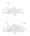
- Figure 1 is a schematic sectional view of a partly formed first embodiment of a transistor according to an embodiment of the invention.
- Figure 2 is a schematic sectional view showing the transistor of Figure 1 at a later stage in formation.
- Figure 3 is a schematic sectional view showing the transistor of Figure 2 at a later stage in formation.
- Figure 4 is a schematic sectional view showing the transistor of Figure 3 at a later stage in formation.
- Figure 5 is a schematic sectional view showing the transistor of Figure 4 at a later stage in formation.
- Figure 6 is a schematic sectional view, similar to Figure 5 , of a second embodiment of a transistor according to an embodiment of the invention.
- Figure 7 is a schematic sectional view, similar to Figure 6 , of a third embodiment of a transistor according to an embodiment of the invention.
- Figure 8 is a schematic sectional view of a partly formed fourth embodiment of a transistor according to an embodiment of the invention.
- Figure 9 is a schematic sectional view showing the transistor of Figure 8 at a later stage in formation.
- Figure 10 is a schematic sectional view, similar to Figure 4 , of a partly formed transistor.
- Figure 11 is a schematic sectional view; similar to Figure 5 , showing the transistor of Figure 10 at a later stage in formation.
- Figure 12 is a schematic sectional view, similar to Figure 6 , of a fifth embodiment of a semiconductor device according to an embodiment of the invention.
- a gate electrode 22 is applied to a substrate 24, and is covered by a dielectric layer 26.
- the gate electrode 22 may be of aluminum, and may then be anodized to form an aluminum oxide dielectric layer approximately 5 to 500 nm thick.
- Anodization is a process whereby a metal is electrochemically oxidized, with voltage applied such that the metal is the anode.
- the gate dielectric 26 may be annealed, for example, by thermal processing.
- the gate electrode 22 may project beyond the dielectric layer 26 at one side, so that there is an exposed part of the gate electrode that can be connected to an electrical circuit.
- the substrate 24 may be part of a larger electrical or electronic circuit structure, and may include a connection to the gate electrode 22. There may be a layer such as an insulator 27 between the larger substrate 24 and the gate electrode 22. An insulator layer 27 may be appropriate, for example, in an embodiment in which the larger substrate 24 is of electrically conductive material.
- the semiconductor material may be, for example, a zinc-tin oxide material, and may be formed, for example, by RF sputtering or by being deposited from a sol-gel precursor that comprises partially hydrolyzed and/or oligomerized metal alkoxides in an alcohol solution.
- the width and thickness of the semiconductor strip 28 affect the current flow through the finished transistor, and so are controlled when the strip is formed.
- the length of the semiconductor strip 28, which is the dimension extending from left to right in Figure 2 is relatively unimportant, provided that it is long enough to contact both the source and drain electrodes, and is not so long as to interfere with neighboring circuit elements.
- the semiconductor strip 28 may be annealed, for example, by laser annealing or by thermal processing.
- a source or drain electrode 30 is then applied over the semiconductor strip 28.
- the basic structure of an FET is sufficiently nearly symmetrical that either the source or the drain may be the electrode 30, or it may not even be determined at this stage which is which.
- the source and drain electrodes may be made of different metals.
- the electrode 30 consists of aluminum, tantalum or another metal that can be anodized, such as tungsten, bismuth, antimony, niobium, or alloys thereof, including alloys of aluminum and tantalum with one another, with the other metals mentioned above, and with Ag, Cd, Cr, Cu, Fe, Mg, Sn, Ti, W, Zn, Zr, and combinations thereof.
- An optional underlayer 31 of some material that forms a better electrical contact with the semiconductor and/or improves adhesion may optionally be applied before the electrode 30 is deposited.
- One edge 32 of the electrode 30 extends substantially across the width of the semiconductor strip 28. The exact position of the edge 32 is unimportant, provided that there is sufficient overlap between the electrode 30 and the semiconductor strip 28 for adequate current transfer between them. The location of the opposite edge of the electrode 30 is also relatively unimportant, although again, there must be provided sufficient overlap between the electrode 30 and the semiconductor strip 28 for adequate current transfer between them.
- the source or drain electrode 30 may project beyond the dielectric layer 26 and the substrate 24 at one side, so that there is an exposed part of the electrode that can be connected to an electrical circuit. However, other methods of connecting to the electrode 30 may be used.
- the edge face 32 may be formed so as to be smooth to a fraction of the intended channel length.
- the electrode 30 may be formed by existing techniques such as sputtering or other vacuum deposition processes in combination with photolithography, imprinting, shadow masking, laser ablation, or the like. By utilizing the single edge face 32, the techniques used are not restricted to techniques capable of fine resolution.
- the source or drain electrode 30 is anodized, to form an insulating layer 34 of oxide.
- One edge 35 of the insulating layer 34 extends substantially across the width of the semiconductor strip 28, parallel to and spaced from the edge 32.
- the anodization is controlled so that the width 36 of the insulating layer 34 between the electrode edge 32 and the insulator edge 35 is equal to the intended channel length of the finished transistor, and the insulating layer is smooth and uniform to a fraction of the intended channel length.
- the width is measured along the surface of the semiconductor strip 28 and in a direction perpendicular to the lines defined by the intersections of edge 32 and 35 and the surface of semiconductor strip 28.
- the edge face 32 is approximately perpendicular to the surface of the semiconductor strip 28, so the width 36 is approximately equal to the thickness of the layer 34.
- the insulating layer 34 may be, for example, approximately 20 nm to 1 ⁇ m thick.
- the channel length may be in the region of a few micrometers, assuming a moderate channel mobility value.
- An insulating layer 34 of this thickness and the appropriate smoothness and uniformity can be formed by existing anodization techniques. In this embodiment, if the insulating layer 34 is more than about 300 nm thick, it may be formed by a two-step anodization process.
- a porous alumina layer can be formed by anodization in an electrolyte based on, for example, oxalic, sulfuric, chromic, and/or phosphoric acid or their mixtures.
- a dense or barrier-type alumina layer can be formed by anodization in an electrolyte based on, for example, citric, boric, or tartaric acid.
- the second source or drain electrode 38 is then applied onto the semiconductor strip 28, abutting the insulating layer 34 that covers the edge 32 of the first source or drain electrode 30.
- the channel length 36 is not affected by the position of either edge of the second source or drain electrode 38, as long as the second electrode 38 extends at least across the nearest edge 35 of insulating layer 34.
- the two electrodes 30 and 38 may even overlap one another, because they are separated by the dielectric layer 34.
- the electrode 38 may be formed by the same techniques as the electrode 30, or by other low-precision deposition and patterning techniques, including inkjet printing, offset lithography, flexography, gravure, extrusion, screen printing, dry electrophotographic (DEP) printing, and liquid electrophotographic (LEP) printing.
- inkjet printing offset lithography, flexography, gravure, extrusion, screen printing
- DEP dry electrophotographic
- LEP liquid electrophotographic
- the positions of none of the edges of the elements 22, 26, 28, 30, 38 affects the channel length, as long as their positions are such as to ensure the necessary overlaps as described above, and none of the elements has to be as small as the channel length.
- the principal properties of the transistor are determined by layer thicknesses.
- the width of the semiconductor strip 28 is typically considerably larger than the channel length 36. None of the steps used in fabricating the transistor 20 requires a patterning resolution fine enough to form the dimension 36 directly. This makes it possible for the transistor 20 to be formed by comparatively simple and economical processes, while simultaneously obtaining a relatively small channel length dimension.
- a second embodiment 40 of a transistor is generally similar to the embodiment 20 shown in Figure 5 , and is made by a method generally similar to that described with reference to Figures 1 to 5 .
- the gate electrode 22 is aluminum, and is covered with a dielectric layer 26 by anodizing.
- the semiconductor layer 28 is zinc tin oxide.
- the electrode 30, which is the drain electrode, is aluminum.
- the insulating layer 34 can be formed by anodizing the aluminum electrode 30 to aluminum oxide.
- the source electrode 38 can be formed of indium tin oxide.
- a third embodiment 50 of a transistor is generally similar to the second embodiment 40.
- the drain electrode 30 can be formed by vacuum sputtering with a shadow mask. As is shown in Figure 7 , the shadow mask produces an edge 52 that tapers away gradually.
- the insulating layer 34 can be formed by anodizing the aluminum electrode 30 to aluminum oxide. Because of the gentle taper of the edge 52, the width of the aluminum oxide layer measured along the underlying semiconductor layer 28, which is the eventual channel length 36, may be substantially greater than the thickness of the aluminum oxide layer. With this embodiment of the transistor 50, the channel length 36 may be, for example, 30 to 40 ⁇ m, even though the thickness of the dielectric layer 34 may be only about a few hundred nanometers.
- the source electrode 38 can be formed of indium tin oxide and in an alternate embodiment can include a gold overlayer 54.
- the edge 52 of the aluminum is etched or otherwise patterned to form an edge face similar to the edge face 32 shown in Figure 5 , roughly perpendicular to the surface of semiconductor layer 28.
- the patterning may be carried out by existing processes, such as conventional photolithography and etching. Because there is considerable tolerance in the position of the edge face 32, and because it is not necessary to form a narrow structure, comparatively low-precision processes can be used.
- the semiconductor strip 28 can be formed directly on the substrate 24, without first forming a gate electrode 22.
- the first source or drain electrode 30 and the anodized oxide covering it are then formed as described with reference to Figures 3 and 4 .
- the second source or drain electrode 62 is applied by a liquid-phase process and can be formed from a material that wets the semiconductor 28 but does not wet the dielectric coating 34.
- the material of the electrode 62 then tends to form a layer of fairly uniform thickness on the semiconductor 28, without spreading up the dielectric layer 34.
- the material of the electrode 62 does not need to adhere strongly to the dielectric layer, provided that it lies close enough to the dielectric layer that the thickness of the dielectric layer 34 accurately determines the channel length 36 between the electrodes 30 and 62.
- a dielectric layer 64 is then deposited over the electrode 62, and optionally over at least a portion of dielectric layer 34.
- a gate electrode 66 is then formed, by any convenient method, over at least a portion of the dielectric layers 34 and 64, so as to cover at least the region defined by the source to drain gap 36.
- the substrate 24, gate 22, gate dielectric 26, semiconductor 28, and first source or drain electrode 30 are formed substantially as described above with reference to Figures 1 to 3 .
- a dielectric layer 74 is then applied over the electrode 30 by a printing process, such as thermal inkjet (TIJ), piezo inkjet, liquid electrophotographic (LEP), dry electrophotographic (DEP), offset lithography, flexography, gravure, extrusion, or screen printing.
- TIJ thermal inkjet
- LEP liquid electrophotographic
- DEP dry electrophotographic
- offset lithography flexography
- gravure extrusion
- screen printing with these printing proccesses, accurate printing of sharp edges is possible, but it is difficult to print very tine lines.
- the minimum line width is currently typically more than 10 ⁇ m.
- the dielectric layer 74 there is considerable tolerance in the width. Only the position of one edge, the right hand edge 75 as seen in Figure 10 , needs to be controlled, because the distance of that edge from the edge of the electrode 30 determines the channel length 76 of the finished transistor 70.
- the printed material 74 that defines the channel length 76 can be chosen from materials such as silane coupling agents, alkane thiols, and other that have a propensity for preferential attachment to the source or drain electrode 30 as opposed to the semiconductor material 28.
- the right-hand edge 75 of the dielectric layer 74 may be aligned to a registration mark that was deposited in the same operation as the electrode 30. or the right-hand edges of the electrode 30 and the dielectric layer 74 may be successively aligned to a registration mark or other suitable datum provided at an earlier stage.
- the second source or drain electrode 78 is then applied by any convenient method, including a printing process.
- the position of the electrode 78 is not critical, provided that the electrode 78 overlaps at least the edge 75 of the dielectric 74, and provided that the electrode 78 does not extend far enough to contact neighboring circuit elements.
- the electrode 78 may be applied by processes, such as LEP, DFP, TIJ, or piezo inkjet, that have an accuracy and/or resolution coarser than the channel length 78,
- a fifth embodiment of semiconductor device is a diode 80.
- the diode 80 is similar to the second form of transistor 40 shown in Figure 6 , except that the diode 80 does not have a gate 22 or gate dielectric 26.
- the electrode 38 which in this embodiment is the drain, is arranged to extend over the entire length 36 of the channel. This extension of the drain 38 effectively acts as a gate hard-wired to the drain.
- the insulating; layer 34 may be formed directly by oxidizing certain metals, including tantalum and tungsten, by heating in air. At temperatures tolerable in forming semiconductor devices, an oxides layer a few hundred nanometers thick may be formed by thermal oxidation in an hour or so.
- the second source or drain electrode (62 in Figure 8 could be formed without using selective wetting, or selective wetting could be used in forming the electrode 38 in Figure 5 if the electrode 38 is formed by a liquid process. It is not necessary for the dielectric 34 to form a strong bond to the semiconductor 28. However, if adhesion between the semiconductor 28 and the dielectric 34 is not good, then liquid phase deposition of the electrode 38 or 62, which might penetrate into any gap at the interface between the semiconductor 28 and the dielectric 34, may not be appropriate.
- An optional wetting layer may be used to promote wetting of the desired surface.
- the wetting layer may be selectively deposited by using a material with specific chemical affinities to the underlying material.
- a repellent layer could be applied to a surface to discourage adhesion of a subsequent deposition.
- a repellent layer could be applied to the dielectric layer 34 to ensure that the material of the electrode 62 does not wet it.
- other layers for example, the insulator 27, that do not prevent the operation of the semiconductor device 20, 30, 40, 50, 60 may be included.
- the transistors shown in Figures 6 and 7 were described as having source and drain electrodes of different metals, and the transistors shown in Figures 5 , 9 , 11 , and 12 were not described as having source and drain electrodes of different metals.
- any of the structures shown may be used with source and drain electrodes of the same or different metals.
- Either the source or the drain electrode may in general be the electrode 30 that is formed first. However, in some cases a specific electrode can be formed first.
- the insulating layer 34 is formed by anodization and only one electrode is of a material capable of being anodized
- the anodizable electrode is the electrode 30 that is formed first.
- the electrode that also acts as the gate is the electrode 38 that is formed second.
Landscapes
- Thin Film Transistor (AREA)
- Bipolar Transistors (AREA)
- Solid State Image Pick-Up Elements (AREA)
- Hall/Mr Elements (AREA)
Abstract
Description
- A field effect transistor (FET) typically comprises a drain electrode and a source electrode connected by a channel of semiconductor material, and a gate electrode separated from the channel by an insulating layer. The length of the channel from the source to the drain affects the properties of the transistor and, in particular, affects the speed at which the transistor can be switched on and off.
-
US 2003/111663 A1 describes a thin film transistor that has, on a transparent substrate, a transparent semiconductor layer containing nitrogen, hydrogen and one or more elements selected from Al, Ga and In, a transparent source electrode and a transparent drain electrode at least partially in contact with the transparent semiconductor layer, and a transparent gate electrode. -
EP 0 273 743 A2 describes an electronic device using an oxide film of a molybdenum-tantalum alloy having a tantalum composition ratio of 50 to 97 atomic percent. The oxide film of the Mo-Ta alloy is higher in resistivity than the oxide film of Ta. Therefore, the TFT and MIM elements using the oxide film of the Mo-Ta alloy have a small leak electric current because of the high resistivity of the oxide film. An anodic oxidation film of the Mo-Ta alloy of a better quality can be formed for a multi-layered insulating film. - It is an object of the invention to provide an improved method for forming a semiconductor device.
- This object is achieved by a method according to claim 1.
-
Figure 1 is a schematic sectional view of a partly formed first embodiment of a transistor according to an embodiment of the invention. -
Figure 2 is a schematic sectional view showing the transistor ofFigure 1 at a later stage in formation. -
Figure 3 is a schematic sectional view showing the transistor ofFigure 2 at a later stage in formation. -
Figure 4 is a schematic sectional view showing the transistor ofFigure 3 at a later stage in formation. -
Figure 5 is a schematic sectional view showing the transistor ofFigure 4 at a later stage in formation. -
Figure 6 is a schematic sectional view, similar toFigure 5 , of a second embodiment of a transistor according to an embodiment of the invention. -
Figure 7 is a schematic sectional view, similar toFigure 6 , of a third embodiment of a transistor according to an embodiment of the invention. -
Figure 8 is a schematic sectional view of a partly formed fourth embodiment of a transistor according to an embodiment of the invention. -
Figure 9 is a schematic sectional view showing the transistor ofFigure 8 at a later stage in formation. -
Figure 10 is a schematic sectional view, similar toFigure 4 , of a partly formed transistor. -
Figure 11 is a schematic sectional view; similar toFigure 5 , showing the transistor ofFigure 10 at a later stage in formation. -
Figure 12 is a schematic sectional view, similar toFigure 6 , of a fifth embodiment of a semiconductor device according to an embodiment of the invention. - Referring to the drawings, and initially to
Figure 1 , in one embodiment of a method of forming a field effect transistor (FET), indicated generally by thereference numeral 20, agate electrode 22 is applied to asubstrate 24, and is covered by adielectric layer 26. In this embodiment thegate electrode 22 may be of aluminum, and may then be anodized to form an aluminum oxide dielectric layer approximately 5 to 500 nm thick. Anodization is a process whereby a metal is electrochemically oxidized, with voltage applied such that the metal is the anode. After deposition the gate dielectric 26 may be annealed, for example, by thermal processing. Thegate electrode 22 may project beyond thedielectric layer 26 at one side, so that there is an exposed part of the gate electrode that can be connected to an electrical circuit. However, other methods of connecting to the gate electrode may be used. Thesubstrate 24 may be part of a larger electrical or electronic circuit structure, and may include a connection to thegate electrode 22. There may be a layer such as aninsulator 27 between thelarger substrate 24 and thegate electrode 22. Aninsulator layer 27 may be appropriate, for example, in an embodiment in which thelarger substrate 24 is of electrically conductive material. - Referring now to
Figure 2 , a strip ofsemiconductor material 28 is applied over the gate dielectric. In this embodiment, the semiconductor material may be, for example, a zinc-tin oxide material, and may be formed, for example, by RF sputtering or by being deposited from a sol-gel precursor that comprises partially hydrolyzed and/or oligomerized metal alkoxides in an alcohol solution. The width and thickness of thesemiconductor strip 28 affect the current flow through the finished transistor, and so are controlled when the strip is formed. As will be explained below, the length of thesemiconductor strip 28, which is the dimension extending from left to right inFigure 2 , is relatively unimportant, provided that it is long enough to contact both the source and drain electrodes, and is not so long as to interfere with neighboring circuit elements. After deposition thesemiconductor strip 28 may be annealed, for example, by laser annealing or by thermal processing. - Referring now to
Figure 3 , a source ordrain electrode 30 is then applied over thesemiconductor strip 28. The basic structure of an FET is sufficiently nearly symmetrical that either the source or the drain may be theelectrode 30, or it may not even be determined at this stage which is which. However, for some purposes the source and drain electrodes may be made of different metals. In this embodiment, theelectrode 30 consists of aluminum, tantalum or another metal that can be anodized, such as tungsten, bismuth, antimony, niobium, or alloys thereof, including alloys of aluminum and tantalum with one another, with the other metals mentioned above, and with Ag, Cd, Cr, Cu, Fe, Mg, Sn, Ti, W, Zn, Zr, and combinations thereof. Anoptional underlayer 31 of some material that forms a better electrical contact with the semiconductor and/or improves adhesion may optionally be applied before theelectrode 30 is deposited. Oneedge 32 of theelectrode 30 extends substantially across the width of thesemiconductor strip 28. The exact position of theedge 32 is unimportant, provided that there is sufficient overlap between theelectrode 30 and thesemiconductor strip 28 for adequate current transfer between them. The location of the opposite edge of theelectrode 30 is also relatively unimportant, although again, there must be provided sufficient overlap between theelectrode 30 and thesemiconductor strip 28 for adequate current transfer between them. The source ordrain electrode 30 may project beyond thedielectric layer 26 and thesubstrate 24 at one side, so that there is an exposed part of the electrode that can be connected to an electrical circuit. However, other methods of connecting to theelectrode 30 may be used. - The
edge face 32 may be formed so as to be smooth to a fraction of the intended channel length. Theelectrode 30 may be formed by existing techniques such as sputtering or other vacuum deposition processes in combination with photolithography, imprinting, shadow masking, laser ablation, or the like. By utilizing thesingle edge face 32, the techniques used are not restricted to techniques capable of fine resolution. - Referring now to
Figure 4 , in this embodiment the source ordrain electrode 30 is anodized, to form aninsulating layer 34 of oxide. Oneedge 35 of theinsulating layer 34 extends substantially across the width of thesemiconductor strip 28, parallel to and spaced from theedge 32. The anodization is controlled so that thewidth 36 of theinsulating layer 34 between theelectrode edge 32 and theinsulator edge 35 is equal to the intended channel length of the finished transistor, and the insulating layer is smooth and uniform to a fraction of the intended channel length. The width is measured along the surface of thesemiconductor strip 28 and in a direction perpendicular to the lines defined by the intersections ofedge semiconductor strip 28. In this embodiment, theedge face 32 is approximately perpendicular to the surface of thesemiconductor strip 28, so thewidth 36 is approximately equal to the thickness of thelayer 34. In this embodiment, theinsulating layer 34 may be, for example, approximately 20 nm to 1 µm thick. For a thin film FET with a switching frequency of several MHz, the channel length may be in the region of a few micrometers, assuming a moderate channel mobility value. Aninsulating layer 34 of this thickness and the appropriate smoothness and uniformity can be formed by existing anodization techniques. In this embodiment, if theinsulating layer 34 is more than about 300 nm thick, it may be formed by a two-step anodization process. First, a porous alumina layer can be formed by anodization in an electrolyte based on, for example, oxalic, sulfuric, chromic, and/or phosphoric acid or their mixtures. Next, a dense or barrier-type alumina layer can be formed by anodization in an electrolyte based on, for example, citric, boric, or tartaric acid. - Referring now to
Figure 5 , the second source ordrain electrode 38 is then applied onto thesemiconductor strip 28, abutting theinsulating layer 34 that covers theedge 32 of the first source ordrain electrode 30. As may be seen fromFigure 5 , there is considerable tolerance in the exact position of the second source ordrain electrode 38 relative to the first source ordrain electrode 30, because thechannel length 36 is not affected by the position of either edge of the second source ordrain electrode 38, as long as thesecond electrode 38 extends at least across thenearest edge 35 ofinsulating layer 34. The twoelectrodes dielectric layer 34. Theelectrode 38 may be formed by the same techniques as theelectrode 30, or by other low-precision deposition and patterning techniques, including inkjet printing, offset lithography, flexography, gravure, extrusion, screen printing, dry electrophotographic (DEP) printing, and liquid electrophotographic (LEP) printing. - The positions of none of the edges of the
elements semiconductor strip 28, which may affect the current-carrying capacity of thetransistor 20, the principal properties of the transistor are determined by layer thicknesses. The width of thesemiconductor strip 28 is typically considerably larger than thechannel length 36. None of the steps used in fabricating thetransistor 20 requires a patterning resolution fine enough to form thedimension 36 directly. This makes it possible for thetransistor 20 to be formed by comparatively simple and economical processes, while simultaneously obtaining a relatively small channel length dimension. - Referring now to
Figure 6 , asecond embodiment 40 of a transistor is generally similar to theembodiment 20 shown inFigure 5 , and is made by a method generally similar to that described with reference toFigures 1 to 5 . In the embodiment shown inFigure 6 , thegate electrode 22 is aluminum, and is covered with adielectric layer 26 by anodizing. Thesemiconductor layer 28 is zinc tin oxide. Theelectrode 30, which is the drain electrode, is aluminum. The insulatinglayer 34 can be formed by anodizing thealuminum electrode 30 to aluminum oxide. The source electrode 38 can be formed of indium tin oxide. - Referring now to
Figure 7 , athird embodiment 50 of a transistor is generally similar to thesecond embodiment 40. In thetransistor 50, thedrain electrode 30 can be formed by vacuum sputtering with a shadow mask. As is shown inFigure 7 , the shadow mask produces anedge 52 that tapers away gradually. The insulatinglayer 34 can be formed by anodizing thealuminum electrode 30 to aluminum oxide. Because of the gentle taper of theedge 52, the width of the aluminum oxide layer measured along theunderlying semiconductor layer 28, which is theeventual channel length 36, may be substantially greater than the thickness of the aluminum oxide layer. With this embodiment of thetransistor 50, thechannel length 36 may be, for example, 30 to 40 µm, even though the thickness of thedielectric layer 34 may be only about a few hundred nanometers. The source electrode 38 can be formed of indium tin oxide and in an alternate embodiment can include agold overlayer 54. - In an alternative form of the third embodiment shown in
Figure 7 , after thealuminum drain electrode 30 is deposited and before it is anodized, theedge 52 of the aluminum is etched or otherwise patterned to form an edge face similar to theedge face 32 shown inFigure 5 , roughly perpendicular to the surface ofsemiconductor layer 28. The patterning may be carried out by existing processes, such as conventional photolithography and etching. Because there is considerable tolerance in the position of theedge face 32, and because it is not necessary to form a narrow structure, comparatively low-precision processes can be used. - Referring now to
Figures 8 and 9 , and initially toFigure 8 , in afourth embodiment 60 of a transistor, thesemiconductor strip 28 can be formed directly on thesubstrate 24, without first forming agate electrode 22. The first source or drainelectrode 30 and the anodized oxide covering it are then formed as described with reference toFigures 3 and4 . The second source or drainelectrode 62 is applied by a liquid-phase process and can be formed from a material that wets thesemiconductor 28 but does not wet thedielectric coating 34. The material of theelectrode 62 then tends to form a layer of fairly uniform thickness on thesemiconductor 28, without spreading up thedielectric layer 34. The material of theelectrode 62 does not need to adhere strongly to the dielectric layer, provided that it lies close enough to the dielectric layer that the thickness of thedielectric layer 34 accurately determines thechannel length 36 between theelectrodes - Referring; now to
Figure 9 , adielectric layer 64 is then deposited over theelectrode 62, and optionally over at least a portion ofdielectric layer 34. Agate electrode 66 is then formed, by any convenient method, over at least a portion of thedielectric layers gap 36. - Referring now to
Figures 10 and 11 , and initially toFigure 10 , in anembodiment 70 of a transistor not falling within the scope of the present invention, thesubstrate 24,gate 22,gate dielectric 26,semiconductor 28, and first source or drainelectrode 30 are formed substantially as described above with reference toFigures 1 to 3 . Adielectric layer 74 is then applied over theelectrode 30 by a printing process, such as thermal inkjet (TIJ), piezo inkjet, liquid electrophotographic (LEP), dry electrophotographic (DEP), offset lithography, flexography, gravure, extrusion, or screen printing. With these printing proccesses, accurate printing of sharp edges is possible, but it is difficult to print very tine lines. The minimum line width is currently typically more than 10 µm. However, for thedielectric layer 74 there is considerable tolerance in the width. Only the position of one edge, theright hand edge 75 as seen inFigure 10 , needs to be controlled, because the distance of that edge from the edge of theelectrode 30 determines thechannel length 76 of thefinished transistor 70. The printedmaterial 74 that defines thechannel length 76 can be chosen from materials such as silane coupling agents, alkane thiols, and other that have a propensity for preferential attachment to the source or drainelectrode 30 as opposed to thesemiconductor material 28. Furthermore, the right-hand edge 75 of thedielectric layer 74 may be aligned to a registration mark that was deposited in the same operation as theelectrode 30. or the right-hand edges of theelectrode 30 and thedielectric layer 74 may be successively aligned to a registration mark or other suitable datum provided at an earlier stage. - Referring now to
Figure 11 , the second source or drainelectrode 78 is then applied by any convenient method, including a printing process. As in the case of the second source or drainelectrode 38 shown inFigure 5 , the position of theelectrode 78 is not critical, provided that theelectrode 78 overlaps at least theedge 75 of the dielectric 74, and provided that theelectrode 78 does not extend far enough to contact neighboring circuit elements. Theelectrode 78 may be applied by processes, such as LEP, DFP, TIJ, or piezo inkjet, that have an accuracy and/or resolution coarser than thechannel length 78, - Referring now to
Figure 12 , a fifth embodiment of semiconductor device according to an embodiment of the invention is adiode 80. Thediode 80 is similar to the second form oftransistor 40 shown inFigure 6 , except that thediode 80 does not have agate 22 orgate dielectric 26. Theelectrode 38, which in this embodiment is the drain, is arranged to extend over theentire length 36 of the channel. This extension of thedrain 38 effectively acts as a gate hard-wired to the drain. - Although the invention has been described and illustrated with reference to exemplary embodiments thereof, it will be understood by those skilled in the art that various changes, omissions, and additions may be made thereto, without departing from the scope of the invention as recited in the attached claims. For example, in another alternative form of these embodiments, the insulating;
layer 34 may be formed directly by oxidizing certain metals, including tantalum and tungsten, by heating in air. At temperatures tolerable in forming semiconductor devices, an oxides layer a few hundred nanometers thick may be formed by thermal oxidation in an hour or so. - The second source or drain electrode (62 in
Figure 8 could be formed without using selective wetting, or selective wetting could be used in forming theelectrode 38 inFigure 5 if theelectrode 38 is formed by a liquid process. It is not necessary for the dielectric 34 to form a strong bond to thesemiconductor 28. However, if adhesion between thesemiconductor 28 and the dielectric 34 is not good, then liquid phase deposition of theelectrode semiconductor 28 and the dielectric 34, may not be appropriate. - An optional wetting layer may be used to promote wetting of the desired surface. The wetting layer may be selectively deposited by using a material with specific chemical affinities to the underlying material. Alternatively, or in addition, a repellent layer could be applied to a surface to discourage adhesion of a subsequent deposition. For example, in
Figure 8 , a repellent layer could be applied to thedielectric layer 34 to ensure that the material of theelectrode 62 does not wet it. In any of the embodiments, other layers, for example, theinsulator 27, that do not prevent the operation of thesemiconductor device - The transistors shown in
Figures 6 and 7 were described as having source and drain electrodes of different metals, and the transistors shown inFigures 5 ,9 ,11 , and12 were not described as having source and drain electrodes of different metals. However, any of the structures shown may be used with source and drain electrodes of the same or different metals. Either the source or the drain electrode may in general be theelectrode 30 that is formed first. However, in some cases a specific electrode can be formed first. For example, if the insulatinglayer 34 is formed by anodization and only one electrode is of a material capable of being anodized, the anodizable electrode is theelectrode 30 that is formed first. For example, in an embodiment such as thediode 80 shown inFigure 12 , the electrode that also acts as the gate is theelectrode 38 that is formed second.
Claims (8)
- A method of forming a semiconductor device (20, 40, 50, 60), comprising:forming a first electrode (30) on and electrically coupled with a semiconductor (28), said first electrode having an edge (32) extending across said semiconductor (28);after forming said first electrode (30), forming an insulator (34) over the semiconductor (28), said insulator (34) adjoining the first electrode (30) and extending a selected distance (36) from said edge (32) of said first electrode (30); andafter forming said insulator (34), forming a second electrode (38, 62) on and electrically coupled with the semiconductor (28) adjoining the insulator (34) such that said second electrode (38, 62) is spaced from said edge (32) of said first electrode (30) by said distance (36),wherein forming said insulator (34) comprises reacting the material of said first electrode (30) to form said insulator (34) of selected thickness on the surface of said first electrode (30).
- A method according to claim 1, wherein forming the insulator (34) comprises at least partially covering the first electrode (30) with the insulator (34).
- A method according to claim 1 or claim 2, wherein forming the second electrode (38) comprises at least partially covering the insulator (34) with the second electrode (38).
- A method according to claim 3 when dependent from claim 2, wherein forming the second electrode (38) comprises at least partially covering with the second electrode (38) the part of the insulator (34) that is at least partially covering the first electrode (30).
- A method according to any of claims 1 to 4, comprising providing a substrate (24), and providing a gate electrode (22) over the substrate, with an insulating layer (26) separating the gate electrode (22) from the semiconductor (28), whereby a transistor (20, 40, 50) is formed.
- A method according to any of claims 1 to 5, comprising forming an insulating layer (64) on the second electrode (62), and forming a gate electrode (66) over said insulator (34) and said insulating layer (64), whereby a transistor (60) is formed.
- A method according to any of claims 1 to 6, wherein forming said second electrode (62) comprises applying a material that wets said semiconductor (28) more readily than said material wets said insulator (34).
- A method according to any of claims 1 to 6, wherein forming said second electrode (38) comprises printing said second electrode (38) on said semiconductor (28) overlapping said insulator (34).
Applications Claiming Priority (2)
| Application Number | Priority Date | Filing Date | Title |
|---|---|---|---|
| US10/975,873 US7291522B2 (en) | 2004-10-28 | 2004-10-28 | Semiconductor devices and methods of making |
| PCT/US2005/034913 WO2006049763A2 (en) | 2004-10-28 | 2005-09-27 | Thin film semiconductor devices and methods of making |
Publications (2)
| Publication Number | Publication Date |
|---|---|
| EP1815529A2 EP1815529A2 (en) | 2007-08-08 |
| EP1815529B1 true EP1815529B1 (en) | 2011-03-23 |
Family
ID=35524954
Family Applications (1)
| Application Number | Title | Priority Date | Filing Date |
|---|---|---|---|
| EP05801974A Ceased EP1815529B1 (en) | 2004-10-28 | 2005-09-27 | Methods of making semiconductor devices |
Country Status (6)
| Country | Link |
|---|---|
| US (2) | US7291522B2 (en) |
| EP (1) | EP1815529B1 (en) |
| CN (1) | CN101053085A (en) |
| DE (1) | DE602005027105D1 (en) |
| TW (1) | TW200616054A (en) |
| WO (1) | WO2006049763A2 (en) |
Families Citing this family (2)
| Publication number | Priority date | Publication date | Assignee | Title |
|---|---|---|---|---|
| US20070040165A1 (en) * | 2005-08-16 | 2007-02-22 | Klaus Dimmler | Method of fabricating organic FETs |
| US20070075365A1 (en) * | 2005-10-03 | 2007-04-05 | Peter Mardilovich | Thin-film transistor and method of making the same |
Family Cites Families (40)
| Publication number | Priority date | Publication date | Assignee | Title |
|---|---|---|---|---|
| US4602192A (en) | 1983-03-31 | 1986-07-22 | Matsushita Electric Industrial Co., Ltd. | Thin film integrated device |
| JPS63166236A (en) | 1986-12-26 | 1988-07-09 | Toshiba Corp | Electronic device |
| US4994401A (en) * | 1987-01-16 | 1991-02-19 | Hosiden Electronics Co., Ltd. | Method of making a thin film transistor |
| JPH065755B2 (en) * | 1987-01-16 | 1994-01-19 | ホシデン株式会社 | Thin film transistor |
| JP2700277B2 (en) * | 1990-06-01 | 1998-01-19 | 株式会社半導体エネルギー研究所 | Method for manufacturing thin film transistor |
| JP3562588B2 (en) * | 1993-02-15 | 2004-09-08 | 株式会社半導体エネルギー研究所 | Method for manufacturing semiconductor device |
| US6713330B1 (en) * | 1993-06-22 | 2004-03-30 | Semiconductor Energy Laboratory Co., Ltd. | Method of fabricating a thin film transistor |
| US6300659B1 (en) * | 1994-09-30 | 2001-10-09 | Semiconductor Energy Laboratory Co., Ltd. | Thin-film transistor and fabrication method for same |
| US5574291A (en) * | 1994-12-09 | 1996-11-12 | Lucent Technologies Inc. | Article comprising a thin film transistor with low conductivity organic layer |
| KR100225098B1 (en) * | 1996-07-02 | 1999-10-15 | 구자홍 | Method of manufacturing thin film transistor |
| TW335503B (en) * | 1996-02-23 | 1998-07-01 | Semiconductor Energy Lab Kk | Semiconductor thin film and manufacturing method and semiconductor device and its manufacturing method |
| US6014189A (en) * | 1996-11-15 | 2000-01-11 | International Business Machines Corporation | Transmissive liquid crystal cell with trench capacitor |
| US5981970A (en) * | 1997-03-25 | 1999-11-09 | International Business Machines Corporation | Thin-film field-effect transistor with organic semiconductor requiring low operating voltages |
| US5946551A (en) * | 1997-03-25 | 1999-08-31 | Dimitrakopoulos; Christos Dimitrios | Fabrication of thin film effect transistor comprising an organic semiconductor and chemical solution deposited metal oxide gate dielectric |
| US6344662B1 (en) * | 1997-03-25 | 2002-02-05 | International Business Machines Corporation | Thin-film field-effect transistor with organic-inorganic hybrid semiconductor requiring low operating voltages |
| TW495635B (en) * | 1997-07-11 | 2002-07-21 | Hitachi Ltd | Liquid crystal display device |
| US6251470B1 (en) * | 1997-10-09 | 2001-06-26 | Micron Technology, Inc. | Methods of forming insulating materials, and methods of forming insulating materials around a conductive component |
| JP4376979B2 (en) * | 1998-01-12 | 2009-12-02 | 株式会社半導体エネルギー研究所 | Method for manufacturing semiconductor device |
| KR100453176B1 (en) * | 1998-06-13 | 2005-04-08 | 엘지.필립스 엘시디 주식회사 | Manufacturing method of liquid crystal display device |
| US6294401B1 (en) * | 1998-08-19 | 2001-09-25 | Massachusetts Institute Of Technology | Nanoparticle-based electrical, chemical, and mechanical structures and methods of making same |
| US6506438B2 (en) * | 1998-12-15 | 2003-01-14 | E Ink Corporation | Method for printing of transistor arrays on plastic substrates |
| US6274412B1 (en) * | 1998-12-21 | 2001-08-14 | Parelec, Inc. | Material and method for printing high conductivity electrical conductors and other components on thin film transistor arrays |
| US6498114B1 (en) * | 1999-04-09 | 2002-12-24 | E Ink Corporation | Method for forming a patterned semiconductor film |
| US6736985B1 (en) * | 1999-05-05 | 2004-05-18 | Agere Systems Inc. | High-resolution method for patterning a substrate with micro-printing |
| JP3318285B2 (en) * | 1999-05-10 | 2002-08-26 | 松下電器産業株式会社 | Method for manufacturing thin film transistor |
| CA2374236C (en) * | 1999-06-21 | 2014-12-23 | Cambridge University Technical Services Limited | Aligned polymers for an organic tft |
| JP3645755B2 (en) * | 1999-09-17 | 2005-05-11 | 日本電気株式会社 | Thin film transistor and manufacturing method thereof |
| US6284562B1 (en) * | 1999-11-17 | 2001-09-04 | Agere Systems Guardian Corp. | Thin film transistors |
| US6621098B1 (en) * | 1999-11-29 | 2003-09-16 | The Penn State Research Foundation | Thin-film transistor and methods of manufacturing and incorporating a semiconducting organic material |
| CN1245769C (en) | 1999-12-21 | 2006-03-15 | 造型逻辑有限公司 | Solution processing |
| JP2001257350A (en) * | 2000-03-08 | 2001-09-21 | Semiconductor Energy Lab Co Ltd | Semiconductor device and manufacturing method thereof |
| US6414164B1 (en) * | 2000-07-12 | 2002-07-02 | International Business Machines Corporation | Synthesis of soluble derivatives of sexithiophene and their use as the semiconducting channels in thin-film filed-effect transistors |
| GB2373095A (en) | 2001-03-09 | 2002-09-11 | Seiko Epson Corp | Patterning substrates with evaporation residues |
| GB0111423D0 (en) * | 2001-05-10 | 2001-07-04 | Koninkl Philips Electronics Nv | An electronic device including a thin film transistor |
| JP2003179233A (en) | 2001-12-13 | 2003-06-27 | Fuji Xerox Co Ltd | Thin film transistor and display element having the same |
| US6555411B1 (en) * | 2001-12-18 | 2003-04-29 | Lucent Technologies Inc. | Thin film transistors |
| GB0130485D0 (en) | 2001-12-21 | 2002-02-06 | Plastic Logic Ltd | Self-aligned printing |
| JP2003229541A (en) * | 2002-01-31 | 2003-08-15 | Sony Corp | Semiconductor storage and manufacturing method thereof |
| US6596569B1 (en) * | 2002-03-15 | 2003-07-22 | Lucent Technologies Inc. | Thin film transistors |
| TW571342B (en) * | 2002-12-18 | 2004-01-11 | Au Optronics Corp | Method of forming a thin film transistor |
-
2004
- 2004-10-28 US US10/975,873 patent/US7291522B2/en not_active Expired - Lifetime
-
2005
- 2005-09-27 CN CN200580036681.6A patent/CN101053085A/en active Pending
- 2005-09-27 DE DE602005027105T patent/DE602005027105D1/en not_active Expired - Lifetime
- 2005-09-27 WO PCT/US2005/034913 patent/WO2006049763A2/en not_active Ceased
- 2005-09-27 EP EP05801974A patent/EP1815529B1/en not_active Ceased
- 2005-09-28 TW TW094133743A patent/TW200616054A/en unknown
-
2007
- 2007-09-14 US US11/855,459 patent/US8823100B2/en active Active
Also Published As
| Publication number | Publication date |
|---|---|
| US7291522B2 (en) | 2007-11-06 |
| EP1815529A2 (en) | 2007-08-08 |
| WO2006049763A3 (en) | 2006-08-03 |
| TW200616054A (en) | 2006-05-16 |
| US20080042201A1 (en) | 2008-02-21 |
| WO2006049763A2 (en) | 2006-05-11 |
| US20060091460A1 (en) | 2006-05-04 |
| CN101053085A (en) | 2007-10-10 |
| DE602005027105D1 (en) | 2011-05-05 |
| US8823100B2 (en) | 2014-09-02 |
Similar Documents
| Publication | Publication Date | Title |
|---|---|---|
| US9711613B2 (en) | Stacked graphene field-effect transistor | |
| US5202274A (en) | Method of fabricating thin film transistor | |
| JPH07273118A (en) | Wiring and electrode formation method | |
| JPH04253342A (en) | Thin film transistor array substrate | |
| US20090309134A1 (en) | Semiconductor device and method of manufacturing the same | |
| TW201310548A (en) | Method of forming a top gate transistor | |
| US8823100B2 (en) | Semiconductor devices and methods of making | |
| EP0641028B1 (en) | A thin film device and a method for fabricating the same | |
| JPH03217059A (en) | thin film transistor | |
| JPH0475670B2 (en) | ||
| US7129181B2 (en) | Sub-resolution gaps generated by controlled over-etching | |
| JPS6146068B2 (en) | ||
| JPS6222536B2 (en) | ||
| JP2570607B2 (en) | Method for manufacturing capacitor | |
| JP2006245589A (en) | Transistor using physical property conversion layer, and operation and manufacturing method thereof | |
| JP4401531B2 (en) | Method for forming fine pattern electrode and optical element | |
| JPH01219721A (en) | Metal insulator construction and liquid crystal display device | |
| JPH05152573A (en) | Thin film transistor and its manufacture | |
| RU2031481C1 (en) | Method of manufacture of semiconductor device with controlling electrode of submicron length | |
| US12513942B2 (en) | Vertical-structure field-effect transistor and manufacturing method therefor | |
| KR102832445B1 (en) | Self-aligned manufacturing method of field effect transistor with edge contact structure | |
| GB2111302A (en) | Thin film transistor | |
| JPH04218926A (en) | Manufacture of thin film transistor | |
| JPH09223803A (en) | Method for manufacturing thin film transistor | |
| JPH04302474A (en) | Thin-film transistor |
Legal Events
| Date | Code | Title | Description |
|---|---|---|---|
| PUAI | Public reference made under article 153(3) epc to a published international application that has entered the european phase |
Free format text: ORIGINAL CODE: 0009012 |
|
| 17P | Request for examination filed |
Effective date: 20070525 |
|
| AK | Designated contracting states |
Kind code of ref document: A2 Designated state(s): DE FR GB |
|
| DAX | Request for extension of the european patent (deleted) | ||
| RBV | Designated contracting states (corrected) |
Designated state(s): DE FR GB |
|
| 17Q | First examination report despatched |
Effective date: 20090709 |
|
| RTI1 | Title (correction) |
Free format text: METHODS OF MAKING SEMICONDUCTOR DEVICES |
|
| GRAP | Despatch of communication of intention to grant a patent |
Free format text: ORIGINAL CODE: EPIDOSNIGR1 |
|
| GRAS | Grant fee paid |
Free format text: ORIGINAL CODE: EPIDOSNIGR3 |
|
| GRAA | (expected) grant |
Free format text: ORIGINAL CODE: 0009210 |
|
| AK | Designated contracting states |
Kind code of ref document: B1 Designated state(s): DE FR GB |
|
| REG | Reference to a national code |
Ref country code: GB Ref legal event code: FG4D |
|
| REF | Corresponds to: |
Ref document number: 602005027105 Country of ref document: DE Date of ref document: 20110505 Kind code of ref document: P |
|
| REG | Reference to a national code |
Ref country code: DE Ref legal event code: R096 Ref document number: 602005027105 Country of ref document: DE Effective date: 20110505 |
|
| REG | Reference to a national code |
Ref country code: DE Ref legal event code: R081 Ref document number: 602005027105 Country of ref document: DE Owner name: HEWLETT-PACKARD DEVELOPMENT COMPANY, L.P., HOU, US Free format text: FORMER OWNER: HEWLETT-PACKARD DEVELOPMENT CO., L.P., FORT COLLINS, COL., US Effective date: 20110420 |
|
| PLBE | No opposition filed within time limit |
Free format text: ORIGINAL CODE: 0009261 |
|
| STAA | Information on the status of an ep patent application or granted ep patent |
Free format text: STATUS: NO OPPOSITION FILED WITHIN TIME LIMIT |
|
| 26N | No opposition filed |
Effective date: 20111227 |
|
| REG | Reference to a national code |
Ref country code: DE Ref legal event code: R097 Ref document number: 602005027105 Country of ref document: DE Effective date: 20111227 |
|
| REG | Reference to a national code |
Ref country code: FR Ref legal event code: PLFP Year of fee payment: 12 |
|
| REG | Reference to a national code |
Ref country code: FR Ref legal event code: PLFP Year of fee payment: 13 |
|
| REG | Reference to a national code |
Ref country code: FR Ref legal event code: PLFP Year of fee payment: 14 |
|
| PGFP | Annual fee paid to national office [announced via postgrant information from national office to epo] |
Ref country code: GB Payment date: 20230823 Year of fee payment: 19 |
|
| PGFP | Annual fee paid to national office [announced via postgrant information from national office to epo] |
Ref country code: FR Payment date: 20230822 Year of fee payment: 19 Ref country code: DE Payment date: 20230822 Year of fee payment: 19 |
|
| REG | Reference to a national code |
Ref country code: DE Ref legal event code: R079 Ref document number: 602005027105 Country of ref document: DE Free format text: PREVIOUS MAIN CLASS: H01L0029786000 Ipc: H10D0030670000 |
|
| REG | Reference to a national code |
Ref country code: DE Ref legal event code: R119 Ref document number: 602005027105 Country of ref document: DE |
|
| GBPC | Gb: european patent ceased through non-payment of renewal fee |
Effective date: 20240927 |
|
| PG25 | Lapsed in a contracting state [announced via postgrant information from national office to epo] |
Ref country code: DE Free format text: LAPSE BECAUSE OF NON-PAYMENT OF DUE FEES Effective date: 20250401 |
|
| PG25 | Lapsed in a contracting state [announced via postgrant information from national office to epo] |
Ref country code: GB Free format text: LAPSE BECAUSE OF NON-PAYMENT OF DUE FEES Effective date: 20240927 |
|
| PG25 | Lapsed in a contracting state [announced via postgrant information from national office to epo] |
Ref country code: FR Free format text: LAPSE BECAUSE OF NON-PAYMENT OF DUE FEES Effective date: 20240930 |