EP1814232A1 - Pipelined analog-to-digital converters - Google Patents
Pipelined analog-to-digital converters Download PDFInfo
- Publication number
- EP1814232A1 EP1814232A1 EP06024141A EP06024141A EP1814232A1 EP 1814232 A1 EP1814232 A1 EP 1814232A1 EP 06024141 A EP06024141 A EP 06024141A EP 06024141 A EP06024141 A EP 06024141A EP 1814232 A1 EP1814232 A1 EP 1814232A1
- Authority
- EP
- European Patent Office
- Prior art keywords
- voltage
- analog
- voltage reference
- digital
- pipelined
- Prior art date
- Legal status (The legal status is an assumption and is not a legal conclusion. Google has not performed a legal analysis and makes no representation as to the accuracy of the status listed.)
- Granted
Links
- 238000013500 data storage Methods 0.000 description 24
- 230000001413 cellular effect Effects 0.000 description 12
- 238000010586 diagram Methods 0.000 description 12
- 230000006870 function Effects 0.000 description 7
- 238000000034 method Methods 0.000 description 7
- 238000004364 calculation method Methods 0.000 description 6
- 230000003287 optical effect Effects 0.000 description 6
- 238000004891 communication Methods 0.000 description 2
- 230000003044 adaptive effect Effects 0.000 description 1
- 230000005540 biological transmission Effects 0.000 description 1
- 238000006243 chemical reaction Methods 0.000 description 1
- 238000012986 modification Methods 0.000 description 1
- 230000004048 modification Effects 0.000 description 1
- 238000013139 quantization Methods 0.000 description 1
- 238000005070 sampling Methods 0.000 description 1
Images


Classifications
-
- H—ELECTRICITY
- H03—ELECTRONIC CIRCUITRY
- H03M—CODING; DECODING; CODE CONVERSION IN GENERAL
- H03M1/00—Analogue/digital conversion; Digital/analogue conversion
- H03M1/12—Analogue/digital converters
- H03M1/14—Conversion in steps with each step involving the same or a different conversion means and delivering more than one bit
- H03M1/145—Conversion in steps with each step involving the same or a different conversion means and delivering more than one bit the steps being performed sequentially in series-connected stages
-
- H—ELECTRICITY
- H03—ELECTRONIC CIRCUITRY
- H03M—CODING; DECODING; CODE CONVERSION IN GENERAL
- H03M1/00—Analogue/digital conversion; Digital/analogue conversion
- H03M1/002—Provisions or arrangements for saving power, e.g. by allowing a sleep mode, using lower supply voltage for downstream stages, using multiple clock domains or by selectively turning on stages when needed
Definitions
- the present disclosure relates to pipelined analog-to-digital converters (ADCs).
- ADCs analog-to-digital converters
- ADCs Analog-to-digital converters
- the ADC may include a pipelined ADC that utilizes multiple stages. Each stage employs a sample and hold circuit that samples an analog Input voltage V in to the pipelined ADC or a residue voltage V res from a prior stage. In addition, each of the stages receives a reference voltage V ref .
- the ADC 10 includes a plurality of stages 12-1, 12-2, and 12-3 (collectively stages 12) that are cascaded in series. Although three stages 12-1, 12-2, and 12-3 are shown, the pipelined ADC 10 may include additional or fewer stages.
- Some of the A/D converter stages 12 include a sample and hold module 14 that samples and holds the analog input signal V in or the residue signal V res from a prior stage.
- a low resolution A/D subconverter module 16 quantizes the held analog signal to a resolution of B i bits where / corresponds to the current stage of the pipelined A/D converter 10.
- the number of bits per stage B i and/or the number of stages may be determined in part by the desired sampling rate and resolution.
- the output of the A/D subconverter module 16 is supplied to a low-resolution D/A subconverter module 18 that converts the resulting digital output signal back into an analog representation.
- the D/A subconverter module 18 may have a resolution that is equivalent to that of the corresponding A/D subconverter module 16 of the same stage.
- a difference module 20 subtracts the analog output from the D/A subconverter module 18 from the voltage input V in to generate a residue signal V res .
- the residue signal V res is equal to the difference between the held analog signal (V in or V res from the prior stage) and the reconstructed analog signal.
- An analog interstage difference module 22 may be used to amplify the residue signal.
- the amplified residue signal is output to the next stage 12-2 of the pipelined ADC 10.
- the first ADC stage 12-1 of the pipelined ADC 10 operates on a most current analog input sample while the second ADC stage 12-2 operates on the amplified residue of the prior input sample.
- the third stage 12-3 operates on the amplified residue output by the second ADC stage 12-2.
- the concurrency of operations allows a conversion speed that is determined by the time it takes in one stage. Once a current stage has completed operating on the analog input sample received from the prior stage, the current stage is available to operate on the next sample.
- a pipelined analog to digital converter comprises a first ADC stage that receives one of an input voltage and a first residue voltage and a first voltage reference and that generates a first digital signal and a second residue voltage.
- a second ADC stage receives the second residue voltage from the first ADC stage and a second voltage reference and that generates a second digital signal.
- the second voltage reference is lower than the first voltage reference.
- a system comprises the pipelined analog to digital converter and further comprises a first voltage source that supplies the first voltage reference.
- a second voltage source supplies the second voltage reference.
- An analog circuit receives the first voltage reference.
- a digital circuit receives the second voltage reference.
- An integrated circuit comprises the pipelined analog to digital converter and further comprises a first voltage source that supplies the first voltage reference.
- a second voltage source supplies the second voltage reference.
- An analog circuit receives the first voltage reference.
- a digital circuit receives the second voltage reference.
- the first ADC stage further comprises a sample and hold module that samples and holds the one of the input voltage and the first residue voltage.
- An analog to digital converter converts an output of the sample and hold module to a digital signal.
- a digital to analog converter converts the digital signal to an analog signal.
- the first ADC stage further comprises a difference module that generates a difference between the output of the sample and hold module and the analog signal.
- An amplifier module amplifies the difference.
- An integrated circuit comprises the pipelined analog to digital converter and further comprises an analog voltage supply that generates the first voltage reference.
- the first voltage reference is an analog voltage reference.
- a digital voltage supply generates the second voltage reference.
- the second voltage reference is a digital voltage reference.
- a system comprises the pipelined analog to digital converter and further comprises an analog voltage supply that generates the first voltage reference.
- the first voltage reference is an analog voltage reference.
- a digital voltage supply generates the second voltage reference.
- the second voltage reference is a digital voltage reference.
- FIG. 1 is a functional block diagram of a pipelined analog to digital converter (ADC) according to the prior art
- FIG. 2 is a functional block diagram of an exemplary pipelined ADC according to the present invention.
- FIG. 3 is a functional block diagram of another exemplary pipelined ADC according to the present invention.
- FIG. 4 is a functional block diagram of an integrated circuit including a pipelined ADC according to the present invention.
- FIG. 5 is a functional block diagram of an integrated circuit including an analog voltage supply, a digital voltage supply, and a pipelined ADC according to the present invention
- FIG. 6A Is a functional block diagram of a hard disk drive
- FIG. 6B is a functional block diagram of a digital versatile disk (DVD).
- DVD digital versatile disk
- FIG. 6C is a functional block diagram of a high definition television
- FIG. 6D is a functional block diagram of a vehicle control system
- FIG. 6E is a functional block diagram of a cellular phone
- FIG. 6F is a functional block diagram of a set top box.
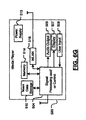
- FIG. 6G is a functional block diagram of a media player.
- module, circuit and/or device refers to an Application Specific Integrated Circuit (ASIC), an electronic circuit, a processor (shared, dedicated, or group) and memory that execute one or more software or firmware programs, a combinational logic circuit, and/or other suitable components that provide the described functionality.
- ASIC Application Specific Integrated Circuit
- processor shared, dedicated, or group
- memory that execute one or more software or firmware programs, a combinational logic circuit, and/or other suitable components that provide the described functionality.
- phrase at least one of A, B, and C should be construed to mean a logical (A or B or C), using a non-exclusive logical or. It should be understood that steps within a method may be executed In different order without altering the principles of the present disclosure.
- a pipelined ADC 100 including multiple voltage references V ref_1 is shown, where / corresponds to the current stage of the pipelined ADC 100.
- the pipelined ADC 100 includes stages 112-1, 112-2, and 112-3 (collectively stages 112), a sample and hold module 114, an ADC module 116, a digital to analog converter (DAC) module 118, a difference module 120 and an amplifier module 122. While three stages are shown, additional or fewer stages can be used.
- the quantization of bits by a subsequent stage of the pipelined ADC 100 does not require the same signal to noise levels (SNR) as the current stage and therefore a lower reference voltage can be used for at least one of the second and third stages.
- SNR signal to noise levels
- the power consumed by stages 112-1, 112-2, and 112-3 of the pipelined ADC 100 is related to the voltage reference of each stage. As a result, the pipelined ADC 100 tends to consume less power than a pipelined ADC having stages supplied with the same voltage reference as shown in FIG. 1.
- a pipelined ADC 120 including different voltage references, V ref_1 is shown, where / corresponds to the current stage of the pipelined A/D converter 120.
- At least one of the voltage references V ref_1 is derived from an analog supply voltage V analog_ref for analog circuits in the system containing the ADC 120 and at least one of the voltage references is derived from a digital supply voltage V digital_ref for digital circuit in the system containing the ADC 120.
- an integrated circuit (IC) 200 is shown.
- One or more power supply 202 supplies unregulated voltage to voltage regulators 204 and 206.
- a first voltage regulator 204 provides analog supply voltages, V analog_ref_1 , V analog_ref_2, ..., and V analog_ref_X , where X is an integer greater than zero.
- a second voltage regulator 206 provides digital supply voltages, V digital_ref_1 , V digital_ref_2 , ..., and V digital_ref_Y , where Y is an integer greater than zero.
- the IC 200 may also include IC components 210 to perform additional circuit functions.
- the first voltage regulator 204 also supplies one or more analog circuits 216 in the IC 200.
- the second voltage regulator 206 also supplies one or more digital circuits 214.
- An integrated circuit (IC) 220 is shown.
- An analog voltage supply 224 generates analog supply voltages, V analog_ref_1' V analog_ref_2 ., and V analog_ref_X , where X is an integer greater than zero.
- a digital voltage supply 226 generates digital supply voltages, V digital_ref_1 , V digital_ref_2 , ..., and V digital_ref_Y , where Y is an integer greater than zero.
- the IC 220 may also include IC components 210 to perform additional circuit functions.
- the analog voltage supply 224 also supplies one or more analog circuits 216 in the IC 200.
- the digital voltage supply 226 also supplies one or more digital circuits 214.
- the device can be implemented in one of more ADCs in a hard disk drive 400.
- the device may implement and/or be implemented in either or both signal processing and/or control circuits, which are generally identified in FIG. 6A at 402 and/or in a power supply 403.
- the signal processing and/or control circuit 402 and/or other circuits (not shown) in the HDD 400 may process data, perform coding and/or encryption, perform calculations, and/or format data that is output to and/or received from a magnetic storage medium 406.
- the HDD 400 may communicate with a host device (not shown) such as a computer, mobile computing devices such as personal digital assistants, cellular phones, media or MP3 players and the like, and/or other devices via one or more wired or wireless communication links 408.
- a host device such as a computer, mobile computing devices such as personal digital assistants, cellular phones, media or MP3 players and the like, and/or other devices via one or more wired or wireless communication links 408.
- the HDD 400 may be connected to memory 409 such as random access memory (RAM).
- RAM random access memory
- ROM read only memory
- the device can be implemented in one of more ADCs in a digital versatile disc (DVD) drive 410.
- the device may implement and/or be implemented in either or both signal processing and/or control circuits, which are generally identified in FIG. 6B at 412, mass data storage of the DVD drive 410 and/or a power supply 413.
- the signal processing and/or control circuit 412 and/or other circuits (not shown) In the DVD 410 may process data, perform coding and/or encryption, perform calculations, and/or format data that is read from and/or data written to an optical storage medium 416.
- the signal processing and/or control circuit 412 and/or other circuits (not shown) in the DVD 410 can also perform other functions such as encoding and/or decoding and/or any other signal processing functions associated with a DVD drive.
- the DVD drive 410 may communicate with an output device (not shown) such as a computer, television or other device via one or more wired or wireless communication links 417.
- the DVD 410 may communicate with mass data storage 418 that stores data in a nonvolatile manner.
- the mass data storage 418 may include a hard disk drive (HDD).
- the HDD may have the configuration shown in FIG. 6A.
- the HDD may be a mini HDD that includes one or more platters having a diameter that is smaller than approximately 1.8".
- the DVD 410 may be connected to memory 419 such as RAM, ROM, low latency nonvolatile memory such as flash memory and/or other suitable electronic data storage.
- the device can be implemented in one of more ADCs in a high definition television (HDTV) 420.
- the device may implement and/or be implemented in either or both signal processing and/or control circuits, which are generally identified in FIG. 6E at 422, a WLAN interface, mass data storage of the HDTV 420 and/or a power supply 423.
- the HDTV 420 receives HDTV input signals in either a wired or wireless format and generates HDTV output signals for a display 426.
- signal processing circuit and/or control circuit 422 and/or other circuits (not shown) of the HDTV 420 may process data, perform coding and/or encryption, perform calculations, format data and/or perform any other type of HDTV processing that may be required.
- the HDTV 420 may communicate with mass data storage 427 that stores data in a nonvolatile manner such as optical and/or magnetic storage devices. At least one HDD may have the configuration shown in FIG. 6A and/or at least one DVD may have the configuration shown in FIG. 6B. The HDD may be a mini HDD that includes one or more platters having a diameter that is smaller than approximately 1,8".
- the HDTV 420 may be connected to memory 428 such as RAM, ROM, low latency nonvolatile memory such as flash memory and/or other suitable electronic data storage.
- the HDTV 420 also may support connections with a WLAN via a WLAN network interface 429.
- the device may implement and/or be implemented in one of more ADCs in a control system of a vehicle 430, a WLAN interface, mass data storage of the vehicle control system and/or a power supply 433.
- the device implement a powertrain control system 432 that receives Inputs from one or more sensors such as temperature sensors, pressure sensors, rotational sensors, airflow sensors and/or any other suitable sensors and/or that generates one or more output control signals such as engine operating parameters, transmission operating parameters, and/or other control signals.
- the device may also be implemented in other control systems 440 of the vehicle 430.
- the control system 440 may likewise receive signals from input sensors 442 and/or output control signals to one or more output devices 444.
- the control system 440 may be part of an anti-lock braking system (ABS), a navigation system, a telematics system, a vehicle telematics system, a lane departure system, an adaptive cruise control system, a vehicle entertainment system such as a stereo, DVD, compact disc and the like. Still other implementations are contemplated.
- the powertrain control system 432 may communicate with mass data storage 446 that stores data in a nonvolatile manner.
- the mass data storage 446 may include optical and/or magnetic storage devices for example hard disk drives HDD and/or DVDs. At least one HDD may have the configuration shown in FIG. 6A and/or at least one DVD may have the configuration shown in FIG. 6B.
- the HDD may be a mini HDD that includes one or more platters having a diameter that is smaller than approximately 1.8".
- the powertrain control system 432 may be connected to memory 447 such as RAM, ROM, low latency nonvolatile memory such as flash memory and/or other suitable electronic data storage.
- the powertrain control system 432 also may support connections with a WLAN via a WLAN network interface 448.
- the control system 440 may also include mass data storage, memory and/or a WLAN interface (all not shown).
- the device can be implemented in one of more ADCs in a cellular phone 450 that may include a cellular antenna 451.
- the device may implement and/or be implemented in either or both signal processing and/or control circuits, which are generally identified in FIG. 6E at 452, a WLAN interface, mass data storage of the cellular phone 450 and/or a power supply 453.
- the cellular phone 450 includes a microphone 456, an audio output 458 such as a speaker and/or audio output jack, a display 460 and/or an input device 462 such as a keypad, pointing device, voice actuation and/or other input device.
- the signal processing and/or control circuits 452 and/or other circuits (not shown) in the cellular phone 450 may process data, perform coding and/or encryption, perform calculations, format data and/or perform other cellular phone functions.
- the cellular phone 450 may communicate with mass data storage 464 that stores data in a nonvolatile manner such as optical and/or magnetic storage devices for example hard disk drives HDD and/or DVDs. At least one HDD may have the configuration shown in FIG. 6A and/or at least one DVD may have the configuration shown in FIG. 6B. The HDD may be a mini HDD that includes one or more platters having a diameter that is smaller than approximately 1.8".
- the cellular phone 450 may be connected to memory 466 such as RAM, ROM, low latency nonvolatile memory such as flash memory and/or other suitable electronic data storage.
- the cellular phone 450 also may support connections with a WLAN via a WLAN network interface 468.
- the device can be implemented in one of more ADCs in a set top box 480.
- the device may implement and/or be Implemented in either or both signal processing and/or control circuits, which are generally identified in FIG. 6F at 484, a WLAN interface, mass data storage of the set top box 480 and/or a power supply 483.
- the set top box 480 receives signals from a source such as a broadband source and outputs standard and/or high definition audio/video signals suitable for a display 488 such as a television and/or monitor and/or other video and/or audio output devices.
- the signal processing and/or control circuits 484 and/or other circuits (not shown) of the set top box 480 may process data, perform coding and/or encryption, perform calculations, format data and/or perform any other set top box function.
- the set top box 480 may communicate with mass data storage 490 that stores data in a nonvolatile manner.
- the mass data storage 490 may include optical and/or magnetic storage devices for example hard disk drives HDD and/or DVDs. At least one HDD may have the configuration shown in FIG. 6A and/or at least one DVD may have the configuration shown in FIG. 6B.
- the HDD may be a mini HDD that includes one or more platters having a diameter that is smaller than approximately 1.8".
- the set top box 480 may be connected to memory 494 such as RAM, ROM, low latency nonvolatile memory such as flash memory and/or other suitable electronic data storage.
- the set top box 480 also may support connections with a WLAN via a WLAN network interface 496.
- the device can be Implemented In one of more ADCs in a media player 500.
- the device may implement and/or be implemented in either or both signal processing and/or control circuits, which are generally identified in FIG. 6G at 504, a WLAN interface, mass data storage of the media player 500 and/or a power supply 503.
- the media player 500 includes a display 507 and/or a user input 508 such as a keypad, touchpad and the like.
- the media player 500 may employ a graphical user Interface (GUI) that typically employs menus, drop down menus, icons and/or a point-and-click Interface via the display 507 and/or user input 508.
- GUI graphical user Interface
- the media player 500 further includes an audio output 509 such as a speaker and/or audio output jack.
- the signal processing and/or control circuits 504 and/or other circuits (not shown) of the media player 500 may process data, perform coding and/or encryption, perform calculations, format data and/or perform any other media player function.
- the media player 500 may communicate with mass data storage 510 that stores data such as compressed audio and/or video content in a nonvolatile manner.
- the compressed audio files include files that are compliant with MP3 format or other suitable compressed audio and/or video formats.
- the mass data storage may include optical and/or magnetic storage devices for example hard disk drives HDD and/or DVDs. At least one HDD may have the configuration shown in FIG. 6A and/or at least one DVD may have the configuration shown in FIG. 6B.
- the HDD may be a mini HDD that includes one or more platters having a diameter that is smaller than approximately 1.8".
- the media player 500 may be connected to memory 514 such as RAM, ROM, low latency nonvolatile memory such as flash memory and/or other suitable electronic data storage.
- the media player 500 also may support connections with a WLAN via a WLAN network interface 516. Still other implementations in addition to those described above are contemplated.
Landscapes
- Engineering & Computer Science (AREA)
- Theoretical Computer Science (AREA)
- Analogue/Digital Conversion (AREA)
- Signal Processing For Digital Recording And Reproducing (AREA)
- Navigation (AREA)
Abstract
Description
- The present disclosure relates to pipelined analog-to-digital converters (ADCs).
- Reducing power consumption of electronic devices has become increasingly important, particularly for battery powered devices such as laptop computers, personal digital assistants, cellular phones, MP3 players and other devices. Analog-to-digital converters (ADCs) are commonly used in these electronic devices to transform analog signals to digital signals. The ADC may include a pipelined ADC that utilizes multiple stages. Each stage employs a sample and hold circuit that samples an analog Input voltage Vin to the pipelined ADC or a residue voltage Vres from a prior stage. In addition, each of the stages receives a reference voltage Vref.
- Referring now to FIG. 1, a typical
pipelined ADC 10 is shown. TheADC 10 includes a plurality of stages 12-1, 12-2, and 12-3 (collectively stages 12) that are cascaded in series. Although three stages 12-1, 12-2, and 12-3 are shown, thepipelined ADC 10 may include additional or fewer stages. Some of the A/D converter stages 12 Include a sample and holdmodule 14 that samples and holds the analog input signal Vin or the residue signal Vres from a prior stage. A low resolution A/D subconverter module 16 quantizes the held analog signal to a resolution of Bi bits where / corresponds to the current stage of the pipelined A/D converter 10. The number of bits per stage B i and/or the number of stages may be determined in part by the desired sampling rate and resolution. The output of the A/D subconverter module 16 is supplied to a low-resolution D/A subconverter module 18 that converts the resulting digital output signal back into an analog representation. - The D/
A subconverter module 18 may have a resolution that is equivalent to that of the corresponding A/D subconverter module 16 of the same stage. Adifference module 20 subtracts the analog output from the D/A subconverter module 18 from the voltage input Vin to generate a residue signal Vres. The residue signal Vres is equal to the difference between the held analog signal (Vin or Vres from the prior stage) and the reconstructed analog signal. - An analog
interstage difference module 22 may be used to amplify the residue signal. The amplified residue signal is output to the next stage 12-2 of the pipelinedADC 10. The first ADC stage 12-1 of the pipelined ADC 10 operates on a most current analog input sample while the second ADC stage 12-2 operates on the amplified residue of the prior input sample. The third stage 12-3 operates on the amplified residue output by the second ADC stage 12-2. - The concurrency of operations allows a conversion speed that is determined by the time it takes in one stage. Once a current stage has completed operating on the analog input sample received from the prior stage, the current stage is available to operate on the next sample.
- A pipelined analog to digital converter comprises a first ADC stage that receives one of an input voltage and a first residue voltage and a first voltage reference and that generates a first digital signal and a second residue voltage. A second ADC stage receives the second residue voltage from the first ADC stage and a second voltage reference and that generates a second digital signal. The second voltage reference is lower than the first voltage reference.
- A system comprises the pipelined analog to digital converter and further comprises a first voltage source that supplies the first voltage reference. A second voltage source supplies the second voltage reference. An analog circuit receives the first voltage reference. A digital circuit receives the second voltage reference.
- An integrated circuit comprises the pipelined analog to digital converter and further comprises a first voltage source that supplies the first voltage reference. A second voltage source supplies the second voltage reference. An analog circuit receives the first voltage reference. A digital circuit receives the second voltage reference.
- In other features, the first ADC stage further comprises a sample and hold module that samples and holds the one of the input voltage and the first residue voltage. An analog to digital converter converts an output of the sample and hold module to a digital signal. A digital to analog converter converts the digital signal to an analog signal. The first ADC stage further comprises a difference module that generates a difference between the output of the sample and hold module and the analog signal. An amplifier module amplifies the difference.
- An integrated circuit comprises the pipelined analog to digital converter and further comprises an analog voltage supply that generates the first voltage reference. The first voltage reference is an analog voltage reference. A digital voltage supply generates the second voltage reference. The second voltage reference is a digital voltage reference.
- A system comprises the pipelined analog to digital converter and further comprises an analog voltage supply that generates the first voltage reference. The first voltage reference is an analog voltage reference. A digital voltage supply generates the second voltage reference. The second voltage reference is a digital voltage reference.
- Further areas of applicability of the present disclosure will become apparent from the detailed description provided hereinafter. It should be understood that the detailed description and specific examples, while indicating the preferred embodiment of the disclosure, are intended for purposes of illustration only and are not intended to limit the scope of the disclosure.
- The present disclosure will become more fully understood from the detailed description and the accompanying drawings, wherein:
- FIG. 1 is a functional block diagram of a pipelined analog to digital converter (ADC) according to the prior art;
- FIG. 2 is a functional block diagram of an exemplary pipelined ADC according to the present invention;
- FIG. 3 is a functional block diagram of another exemplary pipelined ADC according to the present invention;
- FIG. 4 is a functional block diagram of an integrated circuit including a pipelined ADC according to the present invention;
- FIG. 5 is a functional block diagram of an integrated circuit including an analog voltage supply, a digital voltage supply, and a pipelined ADC according to the present invention;
- FIG. 6A Is a functional block diagram of a hard disk drive;
- FIG. 6B is a functional block diagram of a digital versatile disk (DVD);
- FIG. 6C is a functional block diagram of a high definition television;
- FIG. 6D is a functional block diagram of a vehicle control system;
- FIG. 6E is a functional block diagram of a cellular phone;
- FIG. 6F is a functional block diagram of a set top box; and
- FIG. 6G is a functional block diagram of a media player.
- The following description is merely exemplary in nature and is in no way intended to limit the disclosure, its application, or uses. For purposes of clarity, the same reference numbers will be used in the drawings to identify similar elements. As used herein, the term module, circuit and/or device refers to an Application Specific Integrated Circuit (ASIC), an electronic circuit, a processor (shared, dedicated, or group) and memory that execute one or more software or firmware programs, a combinational logic circuit, and/or other suitable components that provide the described functionality. As used herein, the phrase at least one of A, B, and C should be construed to mean a logical (A or B or C), using a non-exclusive logical or. It should be understood that steps within a method may be executed In different order without altering the principles of the present disclosure.
- Referring now to FIG. 2, a pipelined
ADC 100 according to the present invention including multiple voltage references Vref_1 is shown, where / corresponds to the current stage of the pipelinedADC 100. The pipelinedADC 100 includes stages 112-1, 112-2, and 112-3 (collectively stages 112), a sample and holdmodule 114, anADC module 116, a digital to analog converter (DAC)module 118, adifference module 120 and anamplifier module 122. While three stages are shown, additional or fewer stages can be used. In FIG. 2, Vref_1≥ Vref_2 and Vref_1 > Vref_3. The quantization of bits by a subsequent stage of the pipelinedADC 100 does not require the same signal to noise levels (SNR) as the current stage and therefore a lower reference voltage can be used for at least one of the second and third stages. - The power consumed by stages 112-1, 112-2, and 112-3 of the pipelined
ADC 100 is related to the voltage reference of each stage. As a result, the pipelinedADC 100 tends to consume less power than a pipelined ADC having stages supplied with the same voltage reference as shown in FIG. 1. - Referring now to FIG. 3, a pipelined
ADC 120 including different voltage references, Vref_1 is shown, where / corresponds to the current stage of the pipelined A/D converter 120. At least one of the voltage references Vref_1 is derived from an analog supply voltage Vanalog_ref for analog circuits in the system containing theADC 120 and at least one of the voltage references is derived from a digital supply voltage Vdigital_ref for digital circuit in the system containing theADC 120. - Referring now to FIG. 4, an integrated circuit (IC) 200 is shown. One or
more power supply 202 supplies unregulated voltage tovoltage regulators first voltage regulator 204 provides analog supply voltages, Vanalog_ref_1, Vanalog_ref_2,..., and Vanalog_ref_X, where X is an integer greater than zero. Asecond voltage regulator 206 provides digital supply voltages, Vdigital_ref_1, Vdigital_ref_2, ..., and Vdigital_ref_Y, where Y is an integer greater than zero. TheIC 200 may also includeIC components 210 to perform additional circuit functions. Thefirst voltage regulator 204 also supplies one or moreanalog circuits 216 in theIC 200. Thesecond voltage regulator 206 also supplies one or moredigital circuits 214. - Referring now to FIG. 5, an integrated circuit (IC) 220 is shown. An
analog voltage supply 224 generates analog supply voltages, Vanalog_ref_1' Vanalog_ref_2 ....., and Vanalog_ref_X, where X is an integer greater than zero. Adigital voltage supply 226 generates digital supply voltages, Vdigital_ref_1, Vdigital_ref_2, ..., and Vdigital_ref_Y, where Y is an integer greater than zero. TheIC 220 may also includeIC components 210 to perform additional circuit functions. Theanalog voltage supply 224 also supplies one or moreanalog circuits 216 in theIC 200. Thedigital voltage supply 226 also supplies one or moredigital circuits 214. - Referring now to FIGs. 6A-6G, various exemplary implementations of the device are shown. Referring now to FIG. 6A, the device can be implemented in one of more ADCs in a
hard disk drive 400. The device may implement and/or be implemented in either or both signal processing and/or control circuits, which are generally identified in FIG. 6A at 402 and/or in apower supply 403. In some implementations, the signal processing and/orcontrol circuit 402 and/or other circuits (not shown) in theHDD 400 may process data, perform coding and/or encryption, perform calculations, and/or format data that is output to and/or received from amagnetic storage medium 406. - The
HDD 400 may communicate with a host device (not shown) such as a computer, mobile computing devices such as personal digital assistants, cellular phones, media or MP3 players and the like, and/or other devices via one or more wired or wireless communication links 408. TheHDD 400 may be connected tomemory 409 such as random access memory (RAM). low latency nonvolatile memory such as flash memory, read only memory (ROM) and/or other suitable electronic data storage. - Referring now to FIG. 6B, the device can be implemented in one of more ADCs in a digital versatile disc (DVD)
drive 410. The device may implement and/or be implemented in either or both signal processing and/or control circuits, which are generally identified in FIG. 6B at 412, mass data storage of theDVD drive 410 and/or apower supply 413. The signal processing and/orcontrol circuit 412 and/or other circuits (not shown) In theDVD 410 may process data, perform coding and/or encryption, perform calculations, and/or format data that is read from and/or data written to anoptical storage medium 416. In some implementations, the signal processing and/orcontrol circuit 412 and/or other circuits (not shown) in theDVD 410 can also perform other functions such as encoding and/or decoding and/or any other signal processing functions associated with a DVD drive. - The
DVD drive 410 may communicate with an output device (not shown) such as a computer, television or other device via one or more wired or wireless communication links 417. TheDVD 410 may communicate withmass data storage 418 that stores data in a nonvolatile manner. Themass data storage 418 may include a hard disk drive (HDD). The HDD may have the configuration shown in FIG. 6A. The HDD may be a mini HDD that includes one or more platters having a diameter that is smaller than approximately 1.8". TheDVD 410 may be connected tomemory 419 such as RAM, ROM, low latency nonvolatile memory such as flash memory and/or other suitable electronic data storage. - Referring now to FIG. 6C, the device can be implemented in one of more ADCs in a high definition television (HDTV) 420. The device may implement and/or be implemented in either or both signal processing and/or control circuits, which are generally identified in FIG. 6E at 422, a WLAN interface, mass data storage of the
HDTV 420 and/or apower supply 423.] TheHDTV 420 receives HDTV input signals in either a wired or wireless format and generates HDTV output signals for adisplay 426. In some implementations, signal processing circuit and/orcontrol circuit 422 and/or other circuits (not shown) of theHDTV 420 may process data, perform coding and/or encryption, perform calculations, format data and/or perform any other type of HDTV processing that may be required. - The
HDTV 420 may communicate withmass data storage 427 that stores data in a nonvolatile manner such as optical and/or magnetic storage devices. At least one HDD may have the configuration shown in FIG. 6A and/or at least one DVD may have the configuration shown in FIG. 6B. The HDD may be a mini HDD that includes one or more platters having a diameter that is smaller than approximately 1,8". TheHDTV 420 may be connected tomemory 428 such as RAM, ROM, low latency nonvolatile memory such as flash memory and/or other suitable electronic data storage. TheHDTV 420 also may support connections with a WLAN via aWLAN network interface 429. - Referring now to FIG. 6D, the device may implement and/or be implemented in one of more ADCs in a control system of a
vehicle 430, a WLAN interface, mass data storage of the vehicle control system and/or apower supply 433. In some implementations, the device implement apowertrain control system 432 that receives Inputs from one or more sensors such as temperature sensors, pressure sensors, rotational sensors, airflow sensors and/or any other suitable sensors and/or that generates one or more output control signals such as engine operating parameters, transmission operating parameters, and/or other control signals. - The device may also be implemented in
other control systems 440 of thevehicle 430. Thecontrol system 440 may likewise receive signals from input sensors 442 and/or output control signals to one or more output devices 444. In some implementations, thecontrol system 440 may be part of an anti-lock braking system (ABS), a navigation system, a telematics system, a vehicle telematics system, a lane departure system, an adaptive cruise control system, a vehicle entertainment system such as a stereo, DVD, compact disc and the like. Still other implementations are contemplated. - The
powertrain control system 432 may communicate withmass data storage 446 that stores data in a nonvolatile manner. Themass data storage 446 may include optical and/or magnetic storage devices for example hard disk drives HDD and/or DVDs. At least one HDD may have the configuration shown in FIG. 6A and/or at least one DVD may have the configuration shown in FIG. 6B. The HDD may be a mini HDD that includes one or more platters having a diameter that is smaller than approximately 1.8". Thepowertrain control system 432 may be connected tomemory 447 such as RAM, ROM, low latency nonvolatile memory such as flash memory and/or other suitable electronic data storage. Thepowertrain control system 432 also may support connections with a WLAN via aWLAN network interface 448. Thecontrol system 440 may also include mass data storage, memory and/or a WLAN interface (all not shown). - Referring now to FIG. 6E, the device can be implemented in one of more ADCs in a
cellular phone 450 that may include acellular antenna 451. The device may implement and/or be implemented in either or both signal processing and/or control circuits, which are generally identified in FIG. 6E at 452, a WLAN interface, mass data storage of thecellular phone 450 and/or apower supply 453. In some implementations, thecellular phone 450 includes amicrophone 456, anaudio output 458 such as a speaker and/or audio output jack, adisplay 460 and/or aninput device 462 such as a keypad, pointing device, voice actuation and/or other input device. The signal processing and/orcontrol circuits 452 and/or other circuits (not shown) in thecellular phone 450 may process data, perform coding and/or encryption, perform calculations, format data and/or perform other cellular phone functions. - The
cellular phone 450 may communicate withmass data storage 464 that stores data in a nonvolatile manner such as optical and/or magnetic storage devices for example hard disk drives HDD and/or DVDs. At least one HDD may have the configuration shown in FIG. 6A and/or at least one DVD may have the configuration shown in FIG. 6B. The HDD may be a mini HDD that includes one or more platters having a diameter that is smaller than approximately 1.8". Thecellular phone 450 may be connected tomemory 466 such as RAM, ROM, low latency nonvolatile memory such as flash memory and/or other suitable electronic data storage. Thecellular phone 450 also may support connections with a WLAN via aWLAN network interface 468. - Referring now to FIG. 6F, the device can be implemented in one of more ADCs in a set
top box 480. The device may implement and/or be Implemented in either or both signal processing and/or control circuits, which are generally identified in FIG. 6F at 484, a WLAN interface, mass data storage of the settop box 480 and/or apower supply 483. The settop box 480 receives signals from a source such as a broadband source and outputs standard and/or high definition audio/video signals suitable for adisplay 488 such as a television and/or monitor and/or other video and/or audio output devices. The signal processing and/orcontrol circuits 484 and/or other circuits (not shown) of the settop box 480 may process data, perform coding and/or encryption, perform calculations, format data and/or perform any other set top box function. - The set
top box 480 may communicate withmass data storage 490 that stores data in a nonvolatile manner. Themass data storage 490 may include optical and/or magnetic storage devices for example hard disk drives HDD and/or DVDs. At least one HDD may have the configuration shown in FIG. 6A and/or at least one DVD may have the configuration shown in FIG. 6B. The HDD may be a mini HDD that includes one or more platters having a diameter that is smaller than approximately 1.8". The settop box 480 may be connected tomemory 494 such as RAM, ROM, low latency nonvolatile memory such as flash memory and/or other suitable electronic data storage. The settop box 480 also may support connections with a WLAN via aWLAN network interface 496. - Referring now to FIG. 6G, the device can be Implemented In one of more ADCs in a
media player 500. The device may implement and/or be implemented in either or both signal processing and/or control circuits, which are generally identified in FIG. 6G at 504, a WLAN interface, mass data storage of themedia player 500 and/or a power supply 503. In some implementations, themedia player 500 includes adisplay 507 and/or auser input 508 such as a keypad, touchpad and the like. In some implementations, themedia player 500 may employ a graphical user Interface (GUI) that typically employs menus, drop down menus, icons and/or a point-and-click Interface via thedisplay 507 and/oruser input 508. Themedia player 500 further includes anaudio output 509 such as a speaker and/or audio output jack. The signal processing and/orcontrol circuits 504 and/or other circuits (not shown) of themedia player 500 may process data, perform coding and/or encryption, perform calculations, format data and/or perform any other media player function. - The
media player 500 may communicate withmass data storage 510 that stores data such as compressed audio and/or video content in a nonvolatile manner. In some implementations, the compressed audio files include files that are compliant with MP3 format or other suitable compressed audio and/or video formats. The mass data storage may include optical and/or magnetic storage devices for example hard disk drives HDD and/or DVDs. At least one HDD may have the configuration shown in FIG. 6A and/or at least one DVD may have the configuration shown in FIG. 6B. The HDD may be a mini HDD that includes one or more platters having a diameter that is smaller than approximately 1.8". Themedia player 500 may be connected tomemory 514 such as RAM, ROM, low latency nonvolatile memory such as flash memory and/or other suitable electronic data storage. Themedia player 500 also may support connections with a WLAN via aWLAN network interface 516. Still other implementations in addition to those described above are contemplated. - Those skilled in the art can now appreciate from the foregoing description that the broad teachings of the disclosure can be Implemented in a variety of forms. Therefore, while this disclosure includes particular examples, the true scope of the disclosure should not be so limited since other modifications will become apparent to the skilled practitioner upon a study of the drawings, the specification and the following claims.
Claims (10)
- A pipelined analog to digital converter, comprising:a first ADC stage that receives one of an input voltage and a first residue voltage and a first voltage reference and that generates a first digital signal and a second residue voltage; anda second ADC stage that receives said second residue voltage from said first ADC stage and a second voltage reference and that generates a second digital signal, wherein said second voltage reference is lower than said first voltage reference.
- A system comprising the pipelined analog to digital converter of Claim 1 and further comprising:a first voltage source that supplies said first voltage reference; anda second voltage source that supplies said second voltage reference.
- The system of Claim 2 further comprising:an analog circuit that receives said first voltage reference; anda digital circuit that receives said second voltage reference.
- An integrated circuit comprising the pipelined analog to digital converter of Claim 1 and further comprising:a first voltage source that supplies said first voltage reference; anda second voltage source that supplies said second voltage reference.
- The integrated circuit of Claim 4 further comprising:an analog circuit that receives said first voltage reference; anda digital circuit that receives said second voltage reference.
- The pipelined analog to digital converter of Claim 1 wherein said first ADC stage further comprises:a sample and hold module that samples and holds said one of said input voltage and said first residue voltage;an analog to digital converter that converts an output of said sample and hold module to a digital signal; anda digital to analog converter that converts said digital signal to an analog signal.
- The pipelined analog to digital converter of Claim 6 wherein said first ADC stage further comprises:a difference module that generates a difference between said output of said sample and hold module and said analog signal; andan amplifier module that amplifies said difference.
- An integrated circuit comprising the pipelined analog to digital converter of Claim 1 and further comprising:an analog voltage supply that generates said first voltage reference, wherein said first voltage reference is an analog voltage reference; anda digital voltage supply that generates said second voltage reference, wherein said second voltage reference is a digital voltage reference.
- A system comprising the pipelined analog to digital converter of Claim 1 and further comprising an analog voltage supply that generates said first voltage reference, wherein said first voltage reference is an analog voltage reference.
- A system comprising the pipelined analog to digital converter of Claim 1 and further comprising a digital voltage supply that generates said second voltage reference, wherein said second voltage reference is a digital voltage reference.
Applications Claiming Priority (1)
| Application Number | Priority Date | Filing Date | Title |
|---|---|---|---|
| US11/333,935 US7541962B2 (en) | 2006-01-18 | 2006-01-18 | Pipelined analog-to-digital converters |
Publications (2)
| Publication Number | Publication Date |
|---|---|
| EP1814232A1 true EP1814232A1 (en) | 2007-08-01 |
| EP1814232B1 EP1814232B1 (en) | 2013-05-15 |
Family
ID=37685987
Family Applications (1)
| Application Number | Title | Priority Date | Filing Date |
|---|---|---|---|
| EP06024141.1A Ceased EP1814232B1 (en) | 2006-01-18 | 2006-11-21 | Pipelined analog-to-digital converters |
Country Status (6)
| Country | Link |
|---|---|
| US (2) | US7541962B2 (en) |
| EP (1) | EP1814232B1 (en) |
| JP (1) | JP4939201B2 (en) |
| CN (1) | CN101005283B (en) |
| SG (1) | SG134212A1 (en) |
| TW (1) | TWI420827B (en) |
Families Citing this family (8)
| Publication number | Priority date | Publication date | Assignee | Title |
|---|---|---|---|---|
| US7830287B1 (en) * | 2009-05-08 | 2010-11-09 | Himax Media Solutions, Inc. | Analog to digital converter having digital correction logic that utilizes a dither signal to correct a digital code |
| CN101777917B (en) * | 2010-01-14 | 2013-04-03 | 上海迦美信芯通讯技术有限公司 | Pipeline analog-to-digital converter and quick calibration method of capacitance mismatch thereof |
| KR101381250B1 (en) * | 2010-09-15 | 2014-04-04 | 한국전자통신연구원 | Analog digital converting device and reference voltage control method therof |
| CN103247321A (en) * | 2012-02-01 | 2013-08-14 | 宸定股份有限公司 | External mobile device driving system using 3.5 inch hard disk |
| US9143149B1 (en) * | 2014-04-01 | 2015-09-22 | Entropic Communications, LLC. | Method and apparatus for calibration of a time interleaved ADC |
| TWI643185B (en) * | 2017-04-26 | 2018-12-01 | 瑞昱半導體股份有限公司 | Audio processing device and method |
| US10965303B2 (en) * | 2019-08-23 | 2021-03-30 | Analog Devices International Unlimited Company | Data converter system with improved power supply accuracy and sequencing |
| US11258453B2 (en) | 2020-03-09 | 2022-02-22 | SiliconIntervention Inc. | Analog to digital converter |
Citations (8)
| Publication number | Priority date | Publication date | Assignee | Title |
|---|---|---|---|---|
| US5394148A (en) * | 1992-03-04 | 1995-02-28 | Hitachi, Ltd. | AD converter |
| US5682163A (en) * | 1996-03-06 | 1997-10-28 | Industrial Technology Research Institute | Semi-pipelined analog-to-digital converter |
| US5784016A (en) * | 1995-05-02 | 1998-07-21 | Texas Instruments Incorporated | Self-calibration technique for pipe line A/D converters |
| US5966088A (en) * | 1997-05-23 | 1999-10-12 | Mitsubishi Denki Kabushiki Kaisha | Analog/digital converter and voltage comparator capable of fast producing of output offset voltage |
| US6606048B1 (en) * | 2000-11-16 | 2003-08-12 | Marvell International, Ltd. | Method and apparatus for equalizing the digital performance of multiple ADC's |
| US20040189507A1 (en) * | 2003-03-26 | 2004-09-30 | Sanyo Electric Co., Ltd. | Analog-to-digital conversion circuit and image processing circuit for stepwise conversion of a signal through multiple stages of conversion units |
| US6839015B1 (en) * | 2002-12-06 | 2005-01-04 | Marvell International Ltd. | Low power analog to digital converter |
| US20050078025A1 (en) * | 2003-10-09 | 2005-04-14 | Qi Cai | Differential pipelined analog to digital converter with successive approximation register subconverter stages using thermometer coding |
Family Cites Families (9)
| Publication number | Priority date | Publication date | Assignee | Title |
|---|---|---|---|---|
| NL7609608A (en) * | 1976-08-30 | 1978-03-02 | Philips Nv | ANALOG-DIGITAL CONVERTER. |
| US4611196A (en) * | 1985-04-08 | 1986-09-09 | Rca Corporation | Pipelined successive approximation analog-to-digital converter |
| US5771012A (en) * | 1996-09-11 | 1998-06-23 | Harris Corporation | Integrated circuit analog-to-digital converter and associated calibration method and apparatus |
| JP4061033B2 (en) * | 2001-04-18 | 2008-03-12 | 株式会社ルネサステクノロジ | A / D converter and semiconductor integrated circuit |
| JP3942383B2 (en) * | 2001-06-18 | 2007-07-11 | 三洋電機株式会社 | Analog-digital conversion circuit |
| US6710735B1 (en) * | 2003-06-17 | 2004-03-23 | Realter Semiconductor Corp. | Dual supply voltage pipelined ADC |
| US7183962B1 (en) * | 2004-05-17 | 2007-02-27 | Marvell International Ltd. | Low power asynchronous data converter |
| US7161521B2 (en) * | 2004-11-29 | 2007-01-09 | Texas Instruments Incorporated | Multi-stage analog to digital converter architecture |
| KR100688512B1 (en) * | 2004-12-30 | 2007-03-02 | 삼성전자주식회사 | Pipelined Analog-to-Digital Converter Using Two Reference Voltages |
-
2006
- 2006-01-18 US US11/333,935 patent/US7541962B2/en not_active Expired - Fee Related
- 2006-11-21 EP EP06024141.1A patent/EP1814232B1/en not_active Ceased
- 2006-12-15 TW TW095147268A patent/TWI420827B/en not_active IP Right Cessation
- 2006-12-18 CN CN200610168332.6A patent/CN101005283B/en not_active Expired - Fee Related
- 2006-12-18 SG SG200608609-4A patent/SG134212A1/en unknown
- 2006-12-18 JP JP2006340437A patent/JP4939201B2/en not_active Expired - Fee Related
-
2009
- 2009-06-01 US US12/475,947 patent/US7880660B2/en not_active Expired - Lifetime
Patent Citations (8)
| Publication number | Priority date | Publication date | Assignee | Title |
|---|---|---|---|---|
| US5394148A (en) * | 1992-03-04 | 1995-02-28 | Hitachi, Ltd. | AD converter |
| US5784016A (en) * | 1995-05-02 | 1998-07-21 | Texas Instruments Incorporated | Self-calibration technique for pipe line A/D converters |
| US5682163A (en) * | 1996-03-06 | 1997-10-28 | Industrial Technology Research Institute | Semi-pipelined analog-to-digital converter |
| US5966088A (en) * | 1997-05-23 | 1999-10-12 | Mitsubishi Denki Kabushiki Kaisha | Analog/digital converter and voltage comparator capable of fast producing of output offset voltage |
| US6606048B1 (en) * | 2000-11-16 | 2003-08-12 | Marvell International, Ltd. | Method and apparatus for equalizing the digital performance of multiple ADC's |
| US6839015B1 (en) * | 2002-12-06 | 2005-01-04 | Marvell International Ltd. | Low power analog to digital converter |
| US20040189507A1 (en) * | 2003-03-26 | 2004-09-30 | Sanyo Electric Co., Ltd. | Analog-to-digital conversion circuit and image processing circuit for stepwise conversion of a signal through multiple stages of conversion units |
| US20050078025A1 (en) * | 2003-10-09 | 2005-04-14 | Qi Cai | Differential pipelined analog to digital converter with successive approximation register subconverter stages using thermometer coding |
Also Published As
| Publication number | Publication date |
|---|---|
| JP4939201B2 (en) | 2012-05-23 |
| CN101005283A (en) | 2007-07-25 |
| US20090231174A1 (en) | 2009-09-17 |
| SG134212A1 (en) | 2007-08-29 |
| EP1814232B1 (en) | 2013-05-15 |
| US7541962B2 (en) | 2009-06-02 |
| CN101005283B (en) | 2013-03-27 |
| JP2007195159A (en) | 2007-08-02 |
| TW200729740A (en) | 2007-08-01 |
| US20070164891A1 (en) | 2007-07-19 |
| TWI420827B (en) | 2013-12-21 |
| US7880660B2 (en) | 2011-02-01 |
Similar Documents
| Publication | Publication Date | Title |
|---|---|---|
| US7880660B2 (en) | Pipelined analog-to-digital converters | |
| US7768438B1 (en) | Low power analog to digital converter | |
| US7439896B2 (en) | Capacitive digital to analog and analog to digital converters | |
| EP1814221B1 (en) | A variable power adaptice transmitter | |
| KR102958054B1 (en) | Analog-to-digital converter, method of analog-to-digital conversion, and electronic apparatus | |
| US20090024235A1 (en) | Method and apparatus for transmitting and processing audio in inter-ic sound format | |
| EP1814220A1 (en) | A variable power adaptive transmitter | |
| US7388531B1 (en) | Current steering DAC using thin oxide devices | |
| US7586429B1 (en) | Scrambling system for high resolution ditigal-to-analog converter | |
| JP2019201394A (en) | Analog-to-digital converter device and method for generating signal to be tested | |
| WO2022139791A1 (en) | Reconfigurable analog-to-digital converter | |
| US20190373198A1 (en) | Clock Feedthrough Compensation in Image Sensor Systems | |
| HK1109514A (en) | Pipelined analog-to-digital converters | |
| US20230138266A1 (en) | Methods and apparatus to calibrate a dual-residue pipeline analog to digital converter | |
| US7852123B1 (en) | Reset-free comparator with built-in reference | |
| CN101087143A (en) | Method for converting analog signal to digital signal and A/D converter | |
| US12261620B2 (en) | Methods and apparatus to capture switch charge injections and comparator kickback effects | |
| EP1770867B1 (en) | Capacitive digital to analog and analog to digital converters | |
| US20250192796A1 (en) | Methods and apparatus to capture switch charge injections and comparator kickback effects | |
| US7898334B1 (en) | Amplifier with output filtering | |
| US8031821B1 (en) | Digitally assisted power reduction technique for IQ pipeline ADCs used in wireless receivers | |
| US7466572B1 (en) | Three phase voltage tripler | |
| US7576667B1 (en) | Hierarchied calibration circuit | |
| CN118249813A (en) | Method and apparatus for capturing switch charge injection and comparator kickback effects | |
| Xue | An energy-efficient Flash-SAR ADC with two-step flash structure in a 0.18 μm CMOS process |
Legal Events
| Date | Code | Title | Description |
|---|---|---|---|
| PUAI | Public reference made under article 153(3) epc to a published international application that has entered the european phase |
Free format text: ORIGINAL CODE: 0009012 |
|
| AK | Designated contracting states |
Kind code of ref document: A1 Designated state(s): AT BE BG CH CY CZ DE DK EE ES FI FR GB GR HU IE IS IT LI LT LU LV MC NL PL PT RO SE SI SK TR |
|
| AX | Request for extension of the european patent |
Extension state: AL BA HR MK YU |
|
| 17P | Request for examination filed |
Effective date: 20080124 |
|
| 17Q | First examination report despatched |
Effective date: 20080225 |
|
| AKX | Designation fees paid |
Designated state(s): DE FR GB |
|
| GRAP | Despatch of communication of intention to grant a patent |
Free format text: ORIGINAL CODE: EPIDOSNIGR1 |
|
| GRAS | Grant fee paid |
Free format text: ORIGINAL CODE: EPIDOSNIGR3 |
|
| GRAA | (expected) grant |
Free format text: ORIGINAL CODE: 0009210 |
|
| AK | Designated contracting states |
Kind code of ref document: B1 Designated state(s): DE FR GB |
|
| REG | Reference to a national code |
Ref country code: GB Ref legal event code: FG4D |
|
| REG | Reference to a national code |
Ref country code: DE Ref legal event code: R096 Ref document number: 602006036246 Country of ref document: DE Effective date: 20130711 |
|
| PLBE | No opposition filed within time limit |
Free format text: ORIGINAL CODE: 0009261 |
|
| STAA | Information on the status of an ep patent application or granted ep patent |
Free format text: STATUS: NO OPPOSITION FILED WITHIN TIME LIMIT |
|
| 26N | No opposition filed |
Effective date: 20140218 |
|
| REG | Reference to a national code |
Ref country code: DE Ref legal event code: R097 Ref document number: 602006036246 Country of ref document: DE Effective date: 20140218 |
|
| REG | Reference to a national code |
Ref country code: FR Ref legal event code: PLFP Year of fee payment: 10 |
|
| REG | Reference to a national code |
Ref country code: FR Ref legal event code: PLFP Year of fee payment: 11 |
|
| REG | Reference to a national code |
Ref country code: FR Ref legal event code: PLFP Year of fee payment: 12 |
|
| PGFP | Annual fee paid to national office [announced via postgrant information from national office to epo] |
Ref country code: FR Payment date: 20191126 Year of fee payment: 14 |
|
| REG | Reference to a national code |
Ref country code: DE Ref legal event code: R082 Ref document number: 602006036246 Country of ref document: DE Representative=s name: GRUENECKER PATENT- UND RECHTSANWAELTE PARTG MB, DE Ref country code: DE Ref legal event code: R081 Ref document number: 602006036246 Country of ref document: DE Owner name: MARVELL ASIA PTE, LTD., SG Free format text: FORMER OWNER: MARVELL WORLD TRADE LTD., ST. MICHAEL, BB |
|
| REG | Reference to a national code |
Ref country code: GB Ref legal event code: 732E Free format text: REGISTERED BETWEEN 20200709 AND 20200715 |
|
| PGFP | Annual fee paid to national office [announced via postgrant information from national office to epo] |
Ref country code: GB Payment date: 20201126 Year of fee payment: 15 |
|
| PGFP | Annual fee paid to national office [announced via postgrant information from national office to epo] |
Ref country code: DE Payment date: 20210128 Year of fee payment: 15 |
|
| PG25 | Lapsed in a contracting state [announced via postgrant information from national office to epo] |
Ref country code: FR Free format text: LAPSE BECAUSE OF NON-PAYMENT OF DUE FEES Effective date: 20201130 |
|
| REG | Reference to a national code |
Ref country code: DE Ref legal event code: R119 Ref document number: 602006036246 Country of ref document: DE |
|
| GBPC | Gb: european patent ceased through non-payment of renewal fee |
Effective date: 20211121 |
|
| PG25 | Lapsed in a contracting state [announced via postgrant information from national office to epo] |
Ref country code: GB Free format text: LAPSE BECAUSE OF NON-PAYMENT OF DUE FEES Effective date: 20211121 Ref country code: DE Free format text: LAPSE BECAUSE OF NON-PAYMENT OF DUE FEES Effective date: 20220601 |