EP1811662A1 - A lowpass biquad VGA filter - Google Patents
A lowpass biquad VGA filter Download PDFInfo
- Publication number
- EP1811662A1 EP1811662A1 EP06290074A EP06290074A EP1811662A1 EP 1811662 A1 EP1811662 A1 EP 1811662A1 EP 06290074 A EP06290074 A EP 06290074A EP 06290074 A EP06290074 A EP 06290074A EP 1811662 A1 EP1811662 A1 EP 1811662A1
- Authority
- EP
- European Patent Office
- Prior art keywords
- transistor
- terminal
- main
- single ended
- positive
- Prior art date
- Legal status (The legal status is an assumption and is not a legal conclusion. Google has not performed a legal analysis and makes no representation as to the accuracy of the status listed.)
- Granted
Links
- 238000001914 filtration Methods 0.000 abstract description 9
- 238000010586 diagram Methods 0.000 description 8
- 101100228853 Saccharolobus solfataricus (strain ATCC 35092 / DSM 1617 / JCM 11322 / P2) gds gene Proteins 0.000 description 7
- 229920000535 Tan II Polymers 0.000 description 7
- 230000004044 response Effects 0.000 description 7
- 239000000872 buffer Substances 0.000 description 5
- 238000012546 transfer Methods 0.000 description 5
- 230000008901 benefit Effects 0.000 description 3
- 230000008030 elimination Effects 0.000 description 2
- 238000003379 elimination reaction Methods 0.000 description 2
- 238000013459 approach Methods 0.000 description 1
- 239000003990 capacitor Substances 0.000 description 1
- 230000008859 change Effects 0.000 description 1
- 238000006880 cross-coupling reaction Methods 0.000 description 1
- 238000013016 damping Methods 0.000 description 1
- 238000013461 design Methods 0.000 description 1
- 230000001627 detrimental effect Effects 0.000 description 1
- 230000000694 effects Effects 0.000 description 1
- 238000000034 method Methods 0.000 description 1
- 230000003071 parasitic effect Effects 0.000 description 1
- 238000012545 processing Methods 0.000 description 1
- 230000009467 reduction Effects 0.000 description 1
- 238000010079 rubber tapping Methods 0.000 description 1
Images


Classifications
-
- H—ELECTRICITY
- H03—ELECTRONIC CIRCUITRY
- H03H—IMPEDANCE NETWORKS, e.g. RESONANT CIRCUITS; RESONATORS
- H03H11/00—Networks using active elements
- H03H11/02—Multiple-port networks
- H03H11/04—Frequency selective two-port networks
- H03H11/12—Frequency selective two-port networks using amplifiers with feedback
- H03H11/1213—Frequency selective two-port networks using amplifiers with feedback using transistor amplifiers
-
- H—ELECTRICITY
- H03—ELECTRONIC CIRCUITRY
- H03H—IMPEDANCE NETWORKS, e.g. RESONANT CIRCUITS; RESONATORS
- H03H11/00—Networks using active elements
- H03H11/02—Multiple-port networks
- H03H11/04—Frequency selective two-port networks
- H03H11/12—Frequency selective two-port networks using amplifiers with feedback
- H03H11/126—Frequency selective two-port networks using amplifiers with feedback using a single operational amplifier
- H03H11/1286—Sallen-Key biquad
Definitions
- the present invention relates generally to electrical VGA filters and in particular to lowpass biquad VGA filters.
- a lowpass filter is a filter for attenuating or damping the frequency band beyond a given frequency, also called the filter cutoff frequency.
- the amplitude response of a lowpass filter is different for frequencies either above or below the filter cutoff frequency.
- Lowpass filters such as Butterworth, Chebychev or Bessel filters
- These high order filters often present poles only and often consist of several cascaded biquad filters, or biquads.
- a biquad filter is generally a filter with a two pole and two zero filter topology, i.e. with a second order transfer function in the s-domain both in the numerator and denominator. The poles and zeroes are directly linked to the elimination capacities of the biquad filter.
- VGA Variable Gain Amplifier
- ADC Analog to Digital Converter
- a VGA In a typical analog signal chain, a VGA is placed in series with a lowpass filter, however a problem arises in the analog base-band of emerging communications applications where a VGA function is required to amplify a small wide-band signal and a lowpass filter function is required to filter large unwanted blockers.
- An architecture consisting of first filtering the blockers and then amplifying the signal would have the advantage of avoiding non-linearity problems associated with amplifying blockers, but this architecture would suffer from the noise constraints placed upon the filter.
- an architecture consisting of first amplifying the signal and then filtering the blockers would have the advantage of an increased signal to noise ratio (SNR), but would place very difficult non-linearity constraints on the filter.
- SNR signal to noise ratio
- the object of the present invention is to allow these two main functions of a VGA filter without being detrimental to the noise performance or to the linearity of the filter.
- a biquad filter according to claim 1 which has a simple layout, namely with only a few transistors.Therefore such a biquad filter exhibits less current consumption. Furthermore, a low-noise, high Q biquad gain stage is achieved that allows much noise reduction while still minimizing the non-linearity problems at the same time.
- biquad filter can amplify an input signal, it will also be referred to, here after, as a biquad gain stage or biquad filter gain stage.
- the circuit architecture of the proposed biquad filter is based on a well known Sallen-Key biquad circuit, the follower current of which is added to a second current, also derived from the Sallen-Key circuit, to realize the biquad filter transfer function.
- a second aspect of the present invention relates to a lowpass filter as claimed in claim 4 using a plurality of biquad filters as defined in claim 1, all connected in series and powered by the same voltage supply.
- a 2N th order lowpass filter (N being a non nil integer), for example a Butterworth filter, is made of 2N poles. All 2N poles have the same magnitude, but present different angles ⁇ , and thus different values of tan ⁇ . However the 2N poles are actually made up of N pole-pairs, known as complex conjugate pairs.
- the purpose of the biquad filter is to provide a single pole-pair (thus two poles).
- N cascading biquad filters are needed, each providing two poles, or a complex conjugate pole-pair.
- tan ⁇ 4 ⁇ Q 2 - 1 .
- Q factor and tan ⁇ are two ways of indicating the pole positions of a biquad filter. The higher their value is, the harder the circuit is to design. A large tan ⁇ value can be problematic, as the ratio of component values is often related to tan 2 ⁇ .
- both the gain and the filtering are distributed along a signal chain comprising a series of low-noise, high-Q biquad gain stages according to the invention, each with limited current consumption.
- FIG. 1 illustrates a typical Sallen-Key filter circuit.
- the circuit comprises an operational amplifier 10 connected in unity gain. It has positive and negative input terminals 12, 14 and an output terminal 16 connected to the negative input 14.
- First and second conductance g1 and g2 are connected in series between the input Vi of the circuit and the positive input terminal 12 of the amplifier 10.
- a first capacitance C3 is connected between one terminal 22 of the second conductance g2 and the ground 3, or any AC ground node for that matter.
- a second capacitance C4 is connected between a junction 20 between the two first conductances and the output terminal 16 of the amplifier. Naming V22 the output signal on node 22 of FIG.
- the Amp-Op in unity gain arrangement can be replaced by a follower transistor, as shown in FIG. 2.
- the Amp-Op 10 of Fig. 1 is replaced by a follower transistor 40 between the capacitance C4 and node 22.
- the follower transistor comprises two main terminals 41 and 42 and one control terminal 43.
- Capacitance C4 is connected to the second main terminal 42 of the follower transistor.
- Two current sources 30 and 31 have been added. The first one 30 is connected between a first power supply terminal 2 and the first main terminal 41 of the follower transistor, while the second one 31 is connected between the second main terminal 42 of the follower transistor and a second power supply terminal, here the ground 3. Both current sources could deliver the same current, though they could also be used to correct direct current (DC) offsets at the biquad output.
- DC direct current
- the follower transistor itself can be a MOS transistor, either of the NMOS or PMOS type. It could also be an NPN transistor.
- the follower transistor 40 is an NMOS transistor.
- the control terminal 43 of the NMOS transistor is the gate, its first main terminal 41 is the drain and its second main terminal 42 is the source.
- the first power supply terminal delivers a positive DC voltage Vdd, and the second power supply terminal is ground.
- the gate, the drain and the source of the transistor correspond to the same terminals as for an NMOS transistor, while the first power supply terminal is ground, and the second power supply terminal delivers a positive DC voltage Vdd.
- the control terminal 43 of the NPN transistor is the base, its first main terminal 41 is the collector and its second main terminal 42 is the emitter.
- the first power supply terminal of an NPN transistor delivers a positive DC voltage Vdd
- the second power supply terminal is ground.
- the first power supply terminal of a PNP transistor is ground, and the second power supply terminal delivers a positive DC voltage Vdd.
- the man skilled in the art can easily adapt the hereafter examples to alternative circuits using either a PMOS transistor, an NPN or a PNP transistor.
- Transistor 40 is acting as a follower, with the input of the follower connected at the control terminal 43 and the output of the follower connected at the second main terminal 42.
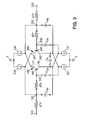
- the general architecture of the differential biquad filter presented on FIG. 3 allows such high tan ⁇ values.
- the architecture is similar to the one of the modified Sallen-Key circuit shown in FIG. 2, and is completed as follows.
- Each single ended circuit comprises a first and second power supply terminal, in this case for example the first power supply terminal delivers a positive DC voltage Vdd, and the second power supply terminal is ground.
- the first single ended circuit hereafter called the positive single ended circuit, further comprises a single input terminal 101 and a single output terminal 102.
- a transistor 140 is also provided, having a control terminal 143, and first main terminal 141 and a second main terminal 142.
- the single output terminal 102 corresponds to the control terminal 143 of the transistor 140.
- a first and second conductances, g1p and g2p are connected in series between the single input terminal 101 and the control terminal 143 of the transistor 140.
- a first current source, or DC current source, 130 is connected between the first power supply terminal 2 and the first main terminal 141 of the transistor 140 while a second current source, or DC current source, 131 is connected between the second main terminal 142 of the transistor 140 and the second power supply terminal 3.
- a first capacitance C3p is connected between the control terminal 143 of the transistor 140 and the second main terminal 242 of the first transistor 240 of the negative single ended circuit.
- a second capacitance C4p connected between the node 120 between the first and second conductances g1p and g2p on one hand, and the second main terminal 142 of the transistor 140 on the other hand.
- the first main terminal 141 is further connected to the node 220 between the first and second conductances g1 n and g2n of the negative single ended circuit.
- the second single ended circuit As the single ended circuits are symmetrical, the second single ended circuit, hereafter called the negative single ended circuit, comprises a single input terminal 201 and a single output terminal 202.
- a transistor 240 is also provided, having a control terminal 243, and first main terminal 241 and a second main terminal 242.
- the single output terminal 202 corresponds to the control terminal 243 of the transistor 240.
- a first and second conductances, g1n and g2n are connected in series between the single input terminal 201 and the control terminal 243 of the transistor 240.
- a first current source, or DC current sink, 230 is connected between the first power supply terminal 2 and the first main terminal 241 of the transistor 240, while a second current source, or DC current source 231 is connected between the second main terminal 242 of the transistor 240 and the second power supply terminal 3.
- a first capacitance C3n is connected between the control terminal 243 of the transistor 240 and the second main terminal 142 of the transistor 140 of the positive single ended circuit.
- a second capacitance C4n connected between the node 220 between the first and second conductances g1n and g2n on one hand, and the second main terminal 242 of the transistor 240 on the other hand.
- the first main terminal 241 is further connected to the node 120 between the first and second conductances g1p and g2n of the negative single ended circuit.
- Both single ended circuits are connected to the same first and second power supply terminals, here Vdd and the ground.
- the differential biquad filter comprising the two single ended circuits further comprises a fifth capacitance C5 connected between the second main terminals 142 and 242 of each transistor 140 and 240 respectively.
- the terminals 101 and 102 of the positive single ended circuit can also be called respectively the positive input and output terminals.
- the terminals 201 and 202 of the negative single ended circuit can also be called respectively the negative input and output terminals.
- transistors 140 and 240 are also called the main transistors of the biquad.
- Rc C ⁇ 4 C ⁇ 3
- Rt C ⁇ 5 C ⁇ 3
- Rg g ⁇ 2 g ⁇ 1
- the component values can be found by choosing g1, Rg (and so g2) and Rt, using equation (3.2) to find Rc, and then using equation (3.5) to find C3 (and so C4 and C5).
- the component values can be found by choosing C3, Rc and Rt (and so C4 and C5), using either equation (3.3) or (3.4) to find Rg, then using equation (3.5) to find g1 (and so g2).
- a novel variation of the circuit of Fig. 3 is to inject a differential signal current using a transconductance GM driven with Vip - Vin.
- the transconductance converts a voltage input signal into a controlled input current signal, where the controlled input current signal produced is equal to the product of the transconductance gain (GM) by the input voltage signal applied to the transconductance.
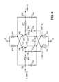
- the circuit of Fig. 3 is modified as follows. First conductances g1 p from the positive single ended circuit, and g1n from the negative single ended circuit, are connected respectively in place of current sources 230 and 130, to yield the circuit of Fig. 4.
- GM.Vip is injected into node 242 (second main terminal of transistor 240) while GM.Vin is injected into node 142 (second main terminal of transistor 140).
- the differential input current signal Isig diff. GM.(Vip - Vin) is injected into the circuit of Fig. 4.
- Biasing current sources 231 and 131 are provided in each single ended circuit to deliver biasing DC current Ibias to the biquad gain stage according to the first embodiment of the invention.
- Biasing current sources are provided to deliver biasing DC current Ibias to each single ended circuit of the biquad gain stage according to the second embodiment of the invention.
- Transconductance GM is characterized by an output current proportional to its input voltage with a small input and output admittance.
- Transconductance GM is connected between an input terminal and one of the nodes mentioned here before. It is in general an active component and in this case is constructed with admittance Yi and a few transistors, including NMOS transistors.Thus, thanks to a transconductance powered by Vip and Vin respectively, to generate current Isig, a gain GM g 1 is implemented without influencing the pole positioning, while simultaneously allowing the elimination of the current sources 130 and 230 respectively, and their associated noise contribution.
- Vop - Von Vip - Vin GM g 1 ⁇ g 1 ⁇ g 2 g 1 ⁇ g 2 + 2 ⁇ s ⁇ g 1 ⁇ C 3 - g 2 ⁇ C 5 + 4 ⁇ s 2 ⁇ C 3 ⁇ C 4 which becomes:
- Vop - Von Vip - Vin g i g 1 ⁇ g 1 ⁇ g 2 g 1 ⁇ g 2 + 2 ⁇ s ⁇ g 1 ⁇ C 3 - g 2 ⁇ C 5 + 4 ⁇ s 2 ⁇ C 3 ⁇ C 4 with the hypothesis that GM is dominated essentially by admittance Yi, here a conductance gi.
- Varying GM using for example well know techniques such as switching conductances, varying bias currents or cross-coupling differential signals, allows the DC gain GM g 1 to be controlled without influencing the pole positioning.
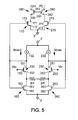
- a transconductance circuit is shown in Fig. 5 and will be described later on.
- biquad gain stage preceded by a transconductance GM, will both provide gain and filtering.
- DC current sinks generating Ibias in the first embodiment may generate noise.
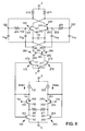
- first current source 231 generates a current Ibias - Isig while first current source 131 generates a current Ibias + Isig thanks to the exemplary GM circuit of Fig. 5.
- the resulting biquad gain stage is shown in FIG. 6 and described later on.
- transconductance GM that is a differential circuit comprising a positive and a negative single ended circuits, each of which including a biasing current source generating a current Ibias.
- Both single ended circuit are symmetrical and will be described hereafter. They respectively correspond to the current sources 231 and 131.
- Each single ended circuit comprises a first 2 and second 3 power supply terminals, in this case for example the first power supply terminal delivers a positive DC voltage Vdd, and the second power supply terminal is ground.
- First and second power supply terminals 2 and 3 correspond to the terminals of the circuit shown in Fig. 4, and are hence given the same numbers.
- the first single ended circuit hereafter called the positive single ended circuit of the GM circuit, comprises a DC current source 132 that delivers bias current Ibias, and a first transistor 150, having a control terminal 153, and a first main terminal 151 and a second main terminal 152.
- DC current source 132 is connected between the first power supply terminal 2 and the first main terminal 151.
- a second transistor 160 having a control terminal 163, and a first main terminal 161 and a second main terminal 162, is also provided on the GM circuit. Its second main terminal 162 is connected to the second power supply terminal 3, while the first main terminal 161 and its control terminal 163 are respectively connected to the second main terminal 152 and the first main terminal 151 of transistor 150.
- a third transistor 170 having a control terminal 173, and a first main terminal 171 and a second main terminal 172, and a fourth transistor 180, having a control terminal 183, and a first main terminal 181 and a second main terminal 182, are further provided on the GM circuit.
- the second main terminal 172 and the control terminal 173 of transistor 170 are respectively connected to the second power supply terminal 3 and the control terminal 163 of transistor 160.
- the first main terminal 171 of transistor 170 is connected to the second main terminal 182 of transistor 180.
- the second single ended circuit As the single ended circuits of the GM circuit are symmetrical, the second single ended circuit, hereafter called the negative single ended circuit, comprises a DC current source 232 that delivers current Ibias, and a first transistor 250, having a control terminal 253, and a first main terminal 251 and a second main terminal 252.
- DC current source 232 is connected between the first power supply terminal 2 and the first main terminal 251.
- a second transistor 260 having a control terminal 263, and a first main terminal 261 and a second main terminal 262, is also provided on the GM circuit. Its second main terminal 262 is connected to the second power supply terminal 3, while its first main terminal 261 and its control terminal 263 is respectively connected to the second main terminal 252 and the first main terminal 251 of transistor 250.
- a third transistor 270 having a control terminal 273, and a first main terminal 271 and a second main terminal 272, and a fourth transistor 280, having a control terminal 283, and a first main terminal 281 and a second main terminal 282, are further provided on the GM circuit.
- the second main terminal 272 and the control terminal 273 of transistor 270 are respectively connected to the second power supply terminal 3 and the control terminal 263 of transistor 260.
- the first main terminal 271 of transistor 270 is connected to the second main terminal 282 of transistor 280.
- Both single ended circuits are connected to the same first and second power supply terminals, in the example of Fig. 5 Vdd and the ground.
- the differential transconductance circuit further comprises two conductances gip and gin connected in series between the second main terminals 152 and 252 of each transistor 150 and 250 respectively.
- control terminals 183 and 283 of transistor 180 and 280 are connected to each other.
- the differential input voltages Vip and Vin are applied to the control terminals the 153 and 253 of transistor 150 and 250 respectively.
- the GM circuit has been chosen for its use of a feedback loop to achieve an accurate gain and good linearity.
- the current sources 132 and 232 ensure that the currents through the input transistors 150 and 250 respectively are constant so that these transistors behave as followers.
- Transconductance GM is connected to the circuit of Fig. 4 by connecting the circuit of Fig. 4 with transistors 180 and 170, i.e. the first main terminal 181 of transistor 180 being connected to the second main terminal 242 of transistor 240, and with transistors 280 and 270, i.e. the first main terminal 281 of transistor 280 being connected to the second main terminal 142 of transistor 140.
- the current through transistor 160 is equal to Ibias - Isig, which corresponds to the current source 231 of the second embodiment, while the current through transistor 260 is equal to Ibias + Isig, which corresponds to the current source 131 of the second embodiment.
- Current through transistor 170 is equal to gm 3 gm 2 ⁇ I bias - I sig
- current through transistor 270 is gm 3 gm 2 ⁇ I bias + I sig
- LG gm 2 Y mir + gds 1 ⁇ Y i gm 1 + gmbs 1 + gds 1 + Y i ⁇ gm 1 + gmbs 1 + gds 1 gm 1 + gmbs 1 + gds 1 + Y i with:
- the DC loop gain may be approximated by: LG DC ⁇ gm 2 g mir ⁇ gm 1 + gmbs 1 gm 1 + gmbs 1 + g i while the dominant pole P L and non dominant pole P H can be approximated by: L L ⁇ g mir C mir and P H ⁇ gm 1 + gmbs 1 + g i C i gi and Ci being respectively the conductance and capacitance of Yi, while gmir and Cmir being respectively the conductance and capacitance of Ymir.
- GM circuit of Fig. 5 provides a linear transconductance proportional to the conductances gip and gin.
- VGA filter with cascaded biquad gain stages, is presented in Fig. 7.
- the VGA filter comprises more precisely 4 gain stages (a mixer stage and 3 biquad gain stages), followed by a pure gain stage (no filtering).
- a mixer stage can consist of a well known Gilbert current multiplier loaded with a conductance and capacitance in order to produce an RF to base-band gain and a single real base-band pole.
- each stage provides a gain of 12dB.
- pole positions (magnitude in MHz, tan ⁇ , and Q factor) are also given in table 1.
- the VGA filter comprises first and second power supply terminals 2, 3, and further comprises a positive input terminal 1101 and a negative input terminal 1201, a positive output terminal 1902 and a negative output terminal 1902.
- the VGA filter also comprises a plurality of biquad gain stages of the type described here above in respect to Fig. 5. In Fig. 7, there are four biquad gain stages cascaded together each as in Fig. 6, preceded by a mixer stage and numbered respectively 10, 30, 50, 70 and 90.
- the differential stages are powered between the first and second power supply terminals 2 and 3.
- the plurality of stages is linked in series with each other. Buffers are required between each stage to isolate the output of the previous biquad from the input of the next. This is common practice for biquads as the buffers are used to isolate the poles of each biquad from outside interference.
- the exemplary VGA filter of Fig. 7 is a 7th order filter with 5 buffers.
- the positive and negative output voltage of one stage correspond to the positive and negative input voltages of a subsequent stage.
- All biquad gain stages comprise a pair of input terminals (positive and negative, driven respectively by the positive and negative input voltages), and a pair of output terminals (positive and negative, from which the positive and negative output voltages are respectively driven).
- Mixer 10 comprises positive and negative input terminals 1101 and 1201 respectively, and positive and negative output terminals 1102 and 1202 respectively.
- First differential biquad 30 comprises positive and negative input terminals 1301 and 1401 respectively, and positive and negative output terminals 1302 and 1402 respectively.
- Second differential biquad 50 comprises positive and negative input terminals 1501 and 1601 respectively, and positive and negative output terminals 1502 and 1602 respectively.
- Third differential biquad 70 comprises positive and negative input terminals 1701 and 1801 respectively, and positive and negative output terminals 1702 and 1802 respectively.
- Pure gain stage 90 comprises positive and negative input terminals 1901 and 2001 respectively, and positive and negative output terminals 1902 and 2002 respectively.
- output terminals 1102 and 1202 are linked to the input terminals 1301 and 1401 respectively, output terminals 1302 and 1402 are linked to the input terminals 1501 and 1601 respectively, output terminals 1502 and 1602 are linked to the input terminals 1701 and 1801 respectively, and output terminals 1702 and 1802 are linked to the input terminals 1901 and 2001 respectively.
- a positive output terminal is linked to a positive input terminal, while a negative output terminal is linked to a negative input terminal.
- the positive and negative input terminals of the whole VGA lowpass filter correspond respectively to the positive and negative input terminals of the first, of the plurality of elementary differential biquad gain stages while the positive and negative output terminals correspond respectively to the positive and negative output terminals of the last of the plurality of differential biquad circuits.
- permutation can be used while linking the positive and negative terminals together.
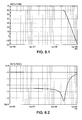
- Fig. 8.1 corresponds to the frequency response while Fig. 8.2 corresponds to the gain.
- gain control is achieved by tapping off various outputs of an R2R resistor network that loads the current mixer.
- the gain control could have been distributed along the chain forming the VGA filter by switching in and out conductance in the transconductance to vary gi.
- a finer gain control is placed at the end of the signal chain to adjust for small variations in the input signal magnitude.
- the differential circuits according to the invention use NMOS transistors, but can alternatively be replaced by PMOS transistors, by inverting the two first and second power supply terminals.
- NMOS transistors are used in the transconductance circuit GM
- a NPN transistor may be used for the main transistors 140 and 240.
- the man skilled in the art can easily adapt the here before architecture to alternative circuits using either PMOS transistors only, or PMOS transistors for the GM circuit and PNP transistors for the main transistors 140 and 240.
Landscapes
- Amplifiers (AREA)
- Networks Using Active Elements (AREA)
Abstract

Description
- The present invention relates generally to electrical VGA filters and in particular to lowpass biquad VGA filters.
- A lowpass filter is a filter for attenuating or damping the frequency band beyond a given frequency, also called the filter cutoff frequency. Thus the amplitude response of a lowpass filter is different for frequencies either above or below the filter cutoff frequency.
- Lowpass filters, such as Butterworth, Chebychev or Bessel filters, have been used for years in the processing of signals in a reverberant or high clutter background. These high order filters often present poles only and often consist of several cascaded biquad filters, or biquads. A biquad filter is generally a filter with a two pole and two zero filter topology, i.e. with a second order transfer function in the s-domain both in the numerator and denominator. The poles and zeroes are directly linked to the elimination capacities of the biquad filter.
- Another type of circuit commonly used in analog signal chains is the Variable Gain Amplifier (VGA). This circuit's function is to amplify a signal in order to drive an Analog to Digital Converter (ADC) with a constant signal magnitude as close as possible to its full swing capacity.
- In a typical analog signal chain, a VGA is placed in series with a lowpass filter, however a problem arises in the analog base-band of emerging communications applications where a VGA function is required to amplify a small wide-band signal and a lowpass filter function is required to filter large unwanted blockers. An architecture consisting of first filtering the blockers and then amplifying the signal would have the advantage of avoiding non-linearity problems associated with amplifying blockers, but this architecture would suffer from the noise constraints placed upon the filter. On the other hand, an architecture consisting of first amplifying the signal and then filtering the blockers would have the advantage of an increased signal to noise ratio (SNR), but would place very difficult non-linearity constraints on the filter.
- Consequently, there is a need for a new VGA filter architecture that integrates together filtering and gain, and that does not display the above mentioned drawbacks from known architectures involving separate VGA and filter functions.
- The object of the present invention is to allow these two main functions of a VGA filter without being detrimental to the noise performance or to the linearity of the filter.
- This is achieved according to a first aspect of the present invention thanks to a biquad filter according to
claim 1 which has a simple layout, namely with only a few transistors.Therefore such a biquad filter exhibits less current consumption. Furthermore, a low-noise, high Q biquad gain stage is achieved that allows much noise reduction while still minimizing the non-linearity problems at the same time. - As the biquad filter according to the invention can amplify an input signal, it will also be referred to, here after, as a biquad gain stage or biquad filter gain stage.
- The circuit architecture of the proposed biquad filter is based on a well known Sallen-Key biquad circuit, the follower current of which is added to a second current, also derived from the Sallen-Key circuit, to realize the biquad filter transfer function.
- A second aspect of the present invention relates to a lowpass filter as claimed in
claim 4 using a plurality of biquad filters as defined inclaim 1, all connected in series and powered by the same voltage supply. - A 2Nth order lowpass filter (N being a non nil integer), for example a Butterworth filter, is made of 2N poles. All 2N poles have the same magnitude, but present different angles θ, and thus different values of tanθ. However the 2N poles are actually made up of N pole-pairs, known as complex conjugate pairs. The purpose of the biquad filter is to provide a single pole-pair (thus two poles). Thus, to build a 2Nth order Butterworth filter, N cascading biquad filters are needed, each providing two poles, or a complex conjugate pole-pair.
- As the order of the filter increases, more biquad filters are required, and the tanθ (or Q factor) values of the last biquad filter gets higher. The Q factor of a biquad is related to the tangent of the biquad pole position (tanθ) by the equation:

- Furthermore, a given number of N structures in parallel will produce

- Thanks to the VGA filter of the invention, both the gain and the filtering are distributed along a signal chain comprising a series of low-noise, high-Q biquad gain stages according to the invention, each with limited current consumption.
- The objects and features of the present invention will become more apparent from the consideration of the following detailed description of exemplary embodiments taken in conjunction with the accompanying drawings, in which:
- FIG. 1 is a schematic circuit diagram of a conventional Sallen-Key filter circuit;
- FIG. 2 is a schematic circuit diagram of a modified Sallen-Key filter circuit;
- FIG. 3 is a structural circuit diagram of a differential Sallen-Key biquad circuit modified for high tanθ values;
- FIG. 4 is a structural circuit diagram of a biquad gain stage with high tanθ and possibility of gain according to a first aspect of the present invention;
- FIG. 5 is a structural circuit diagram of an example of transconductance circuit used in the biquad gain stage according to a first aspect of the present invention;
- FIG. 6 is a structural circuit diagram of the complete biquad gain stage according a first aspect of the present invention;
- FIG. 7 is a structural circuit diagram of the Variable Gain Amplifier filter according to a second aspect of the invention;
- FIG. 8.1 and 8.2 are diagrams showing the gain and frequency response respectively of an application of the Variable Gain Amplifier Filter comprising a mixer gain stage, 3 biquad gain stages (as shown in Fig. 7), and a pure gain stage (as shown in Fig. 7 but with all capacitors removed and with conductances g2 shorted).
- On the different figures, the same elements carry the same reference numbers.
- FIG. 1 illustrates a typical Sallen-Key filter circuit. The circuit comprises an
operational amplifier 10 connected in unity gain. It has positive andnegative input terminals output terminal 16 connected to thenegative input 14. First and second conductance g1 and g2 are connected in series between the input Vi of the circuit and thepositive input terminal 12 of theamplifier 10. A first capacitance C3 is connected between oneterminal 22 of the second conductance g2 and theground 3, or any AC ground node for that matter. A second capacitance C4 is connected between ajunction 20 between the two first conductances and theoutput terminal 16 of the amplifier. Naming V22 the output signal onnode 22 of FIG. 1 and Vi the input signal onnode 1, the Sallen-Key filter circuit yields the following relationship (1.1):
- The main advantage of the Sallen-Key architecture is the simplicity of its implementation.
- The Amp-Op in unity gain arrangement can be replaced by a follower transistor, as shown in FIG. 2. In this figure, the Amp-
Op 10 of Fig. 1 is replaced by afollower transistor 40 between the capacitance C4 andnode 22. The follower transistor comprises twomain terminals control terminal 43. Capacitance C4 is connected to the secondmain terminal 42 of the follower transistor. Twocurrent sources power supply terminal 2 and the firstmain terminal 41 of the follower transistor, while the second one 31 is connected between the secondmain terminal 42 of the follower transistor and a second power supply terminal, here theground 3. Both current sources could deliver the same current, though they could also be used to correct direct current (DC) offsets at the biquad output. - The follower transistor itself can be a MOS transistor, either of the NMOS or PMOS type. It could also be an NPN transistor. In the examples shown hereafter, the
follower transistor 40 is an NMOS transistor. Thus thecontrol terminal 43 of the NMOS transistor is the gate, its firstmain terminal 41 is the drain and its secondmain terminal 42 is the source. The first power supply terminal delivers a positive DC voltage Vdd, and the second power supply terminal is ground. - If a PMOS transistor is chosen, the gate, the drain and the source of the transistor correspond to the same terminals as for an NMOS transistor, while the first power supply terminal is ground, and the second power supply terminal delivers a positive DC voltage Vdd. If an NPN transistor is chosen, the
control terminal 43 of the NPN transistor is the base, its firstmain terminal 41 is the collector and its secondmain terminal 42 is the emitter. The first power supply terminal of an NPN transistor delivers a positive DC voltage Vdd, and the second power supply terminal is ground. The first power supply terminal of a PNP transistor is ground, and the second power supply terminal delivers a positive DC voltage Vdd. The man skilled in the art can easily adapt the hereafter examples to alternative circuits using either a PMOS transistor, an NPN or a PNP transistor. -
Transistor 40 is acting as a follower, with the input of the follower connected at thecontrol terminal 43 and the output of the follower connected at the secondmain terminal 42. - However, the disadvantage of this architecture is that large component ratios are required. If


- From relation (2), it can be appreciated that this architecture is not suitable for generating complex pole pairs with high tanθ values.
- The general architecture of the differential biquad filter presented on FIG. 3 allows such high tanθ values. The architecture is similar to the one of the modified Sallen-Key circuit shown in FIG. 2, and is completed as follows.
- It further comprises a positive and a negative single ended circuit. Both single ended circuits are symmetrical and will be described hereafter. Each single ended circuit comprises a first and second power supply terminal, in this case for example the first power supply terminal delivers a positive DC voltage Vdd, and the second power supply terminal is ground.
- The first single ended circuit, hereafter called the positive single ended circuit, further comprises a
single input terminal 101 and asingle output terminal 102. Atransistor 140 is also provided, having acontrol terminal 143, and firstmain terminal 141 and a secondmain terminal 142. Thesingle output terminal 102 corresponds to thecontrol terminal 143 of thetransistor 140. A first and second conductances, g1p and g2p are connected in series between thesingle input terminal 101 and thecontrol terminal 143 of thetransistor 140. A first current source, or DC current source, 130 is connected between the firstpower supply terminal 2 and the firstmain terminal 141 of thetransistor 140 while a second current source, or DC current source, 131 is connected between the secondmain terminal 142 of thetransistor 140 and the secondpower supply terminal 3. A first capacitance C3p is connected between thecontrol terminal 143 of thetransistor 140 and the secondmain terminal 242 of thefirst transistor 240 of the negative single ended circuit. A second capacitance C4p connected between thenode 120 between the first and second conductances g1p and g2p on one hand, and the secondmain terminal 142 of thetransistor 140 on the other hand. The firstmain terminal 141 is further connected to thenode 220 between the first and second conductances g1 n and g2n of the negative single ended circuit. - As the single ended circuits are symmetrical, the second single ended circuit, hereafter called the negative single ended circuit, comprises a
single input terminal 201 and asingle output terminal 202. Atransistor 240 is also provided, having acontrol terminal 243, and firstmain terminal 241 and a secondmain terminal 242. Thesingle output terminal 202 corresponds to thecontrol terminal 243 of thetransistor 240. A first and second conductances, g1n and g2n are connected in series between thesingle input terminal 201 and thecontrol terminal 243 of thetransistor 240. A first current source, or DC current sink, 230 is connected between the firstpower supply terminal 2 and the firstmain terminal 241 of thetransistor 240, while a second current source, or DCcurrent source 231 is connected between the secondmain terminal 242 of thetransistor 240 and the secondpower supply terminal 3. A first capacitance C3n is connected between thecontrol terminal 243 of thetransistor 240 and the secondmain terminal 142 of thetransistor 140 of the positive single ended circuit. A second capacitance C4n connected between thenode 220 between the first and second conductances g1n and g2n on one hand, and the secondmain terminal 242 of thetransistor 240 on the other hand. The firstmain terminal 241 is further connected to thenode 120 between the first and second conductances g1p and g2n of the negative single ended circuit. - Both single ended circuits are connected to the same first and second power supply terminals, here Vdd and the ground. The differential biquad filter comprising the two single ended circuits further comprises a fifth capacitance C5 connected between the second
main terminals transistor - The
terminals terminals - As other transistors will be referred to hereafter,
transistors - If Vip and Vin are respectively the potentials of the
input terminal output terminals 
where g1n=g1p=g1; g2n=g2p=g2; C3n=C3p=C3; and C4n=C4p=C4, as the differential singled ended circuits are symmetrical. - If


- Assuming that |P| is the pole of the differential biquad filter, and given that


- Thus the component values can be found by choosing g1, Rg (and so g2) and Rt, using equation (3.2) to find Rc, and then using equation (3.5) to find C3 (and so C4 and C5). Alternatively, the component values can be found by choosing C3, Rc and Rt (and so C4 and C5), using either equation (3.3) or (3.4) to find Rg, then using equation (3.5) to find g1 (and so g2).
- Rather then driving the conductances g1 p and g1n with input voltage V1p and V1n respectively, a novel variation of the circuit of Fig. 3 is to inject a differential signal current using a transconductance GM driven with Vip - Vin. The transconductance converts a voltage input signal into a controlled input current signal, where the controlled input current signal produced is equal to the product of the transconductance gain (GM) by the input voltage signal applied to the transconductance. To that effect, the circuit of Fig. 3 is modified as follows. First conductances g1 p from the positive single ended circuit, and g1n from the negative single ended circuit, are connected respectively in place of
current sources - In a first embodiment of the biquad gain stage according to the invention, input current signal Isig = GM.Vip is injected into
node 120 while input current signal GM.Vin is injected intonode 220 as seen in Fig. 4. In another embodiment of the biquad gain stage according to the invention, hereafter referred to as second embodiment or second solution, GM.Vip is injected into node 242 (second main terminal of transistor 240) while GM.Vin is injected into node 142 (second main terminal of transistor 140). Thus the differential input current signal Isig diff. = GM.(Vip - Vin) is injected into the circuit of Fig. 4. - In the first embodiment, an input current signal Isig = GM.Vip is injected into
node 120, while an input current signal Isig = GM.Vin is injected intonode 220. Biasingcurrent sources - In the second embodiment, the new circuit is equivalent to first
current source 231 generating a current Ibias - Isig = Ibias - GM.Vip, i.e. a biasing current to which the input current signal Isig is subtracted, and to firstcurrent source 131 generating a current Ibias + Isig = Ibias + GM.Vin, i.e. the sum of a biasing current signal and the input current signal. Biasing current sources are provided to deliver biasing DC current Ibias to each single ended circuit of the biquad gain stage according to the second embodiment of the invention. - Transconductance GM is characterized by an output current proportional to its input voltage with a small input and output admittance. Transconductance GM is connected between an input terminal and one of the nodes mentioned here before. It is in general an active component and in this case is constructed with admittance Yi and a few transistors, including NMOS transistors.Thus, thanks to a transconductance powered by Vip and Vin respectively, to generate current Isig, a
gain 
current sources 

- Varying GM, using for example well know techniques such as switching conductances, varying bias currents or cross-coupling differential signals, allows the DC gain

- An example of a transconductance circuit is shown in Fig. 5 and will be described later on. The simplest type of transconductance known is as a "differential pair transconductance". With an NMOS differential pair, the total transconductance is given by GM=gmNMOS (where gmNMOS is the NMOS transconductance). If such a differential pair is used to inject current into the biquad gain stage of Fig. 4, the DC gain of equation (4) would become:

- Thus the biquad gain stage according to the invention, preceded by a transconductance GM, will both provide gain and filtering.
- Analysis of all biquads have so far assumed an ideal follower transistor, i.e. for Fig. 3, that V102 - V202 = V142 - V242 for
follower transistors transistors 140 and 240) follower's finite transconductance term gmN. - As unity gain is desired for the
follower transistors 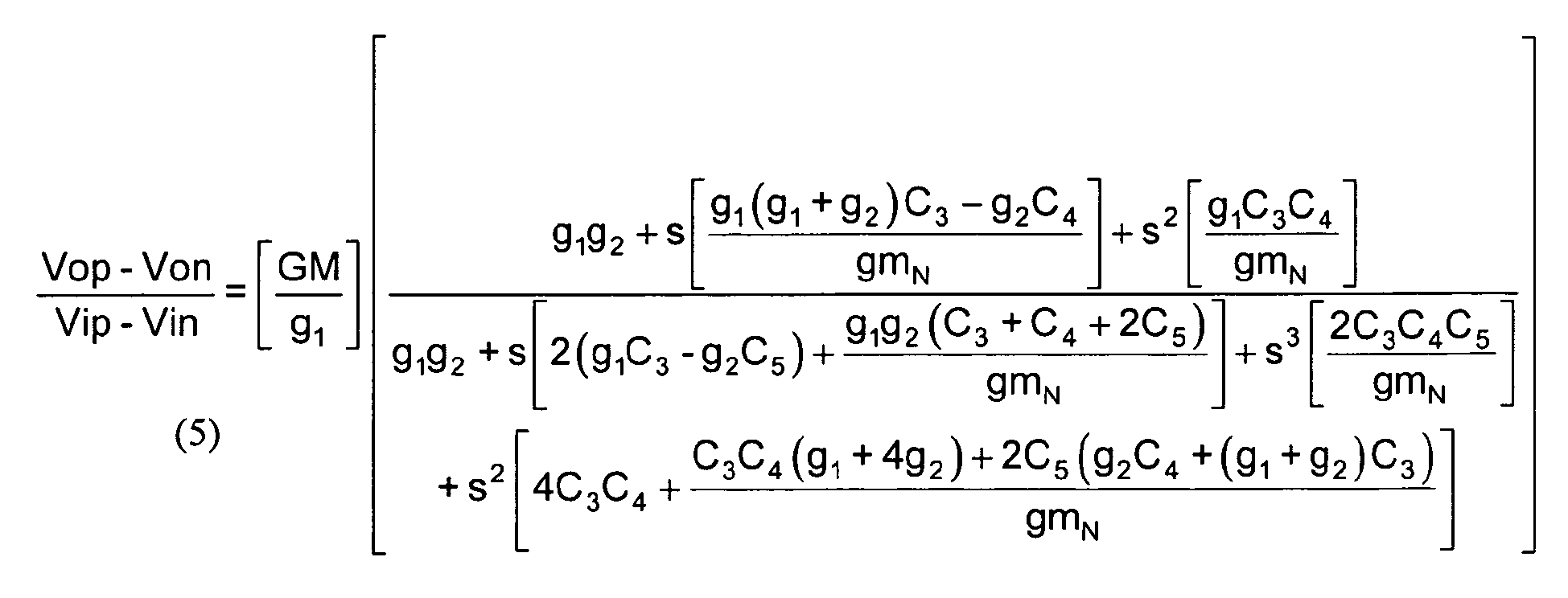
- It can be seen from (5) that gmN needs to be large enough to render the parasitic 1/gmN terms negligible within the frequency band of interest.
- DC current sinks generating Ibias in the first embodiment may generate noise. In order to reduce such noise, in a preferred implementation of the invention, first
current source 231 generates a current Ibias - Isig while firstcurrent source 131 generates a current Ibias + Isig thanks to the exemplary GM circuit of Fig. 5. The resulting biquad gain stage is shown in FIG. 6 and described later on. - To generate Ibias - Isig, and Ibias + Isig respectively, transconductance GM that is a differential circuit comprising a positive and a negative single ended circuits, each of which including a biasing current source generating a current Ibias. Both single ended circuit are symmetrical and will be described hereafter. They respectively correspond to the
current sources power supply terminals - The first single ended circuit, hereafter called the positive single ended circuit of the GM circuit, comprises a DC
current source 132 that delivers bias current Ibias, and afirst transistor 150, having acontrol terminal 153, and a firstmain terminal 151 and a secondmain terminal 152. DCcurrent source 132 is connected between the firstpower supply terminal 2 and the firstmain terminal 151. Asecond transistor 160, having acontrol terminal 163, and a firstmain terminal 161 and a secondmain terminal 162, is also provided on the GM circuit. Its secondmain terminal 162 is connected to the secondpower supply terminal 3, while the firstmain terminal 161 and itscontrol terminal 163 are respectively connected to the secondmain terminal 152 and the firstmain terminal 151 oftransistor 150. Athird transistor 170, having acontrol terminal 173, and a firstmain terminal 171 and a secondmain terminal 172, and afourth transistor 180, having acontrol terminal 183, and a firstmain terminal 181 and a secondmain terminal 182, are further provided on the GM circuit. The secondmain terminal 172 and thecontrol terminal 173 oftransistor 170 are respectively connected to the secondpower supply terminal 3 and thecontrol terminal 163 oftransistor 160. The firstmain terminal 171 oftransistor 170 is connected to the secondmain terminal 182 oftransistor 180. - As the single ended circuits of the GM circuit are symmetrical, the second single ended circuit, hereafter called the negative single ended circuit, comprises a DC
current source 232 that delivers current Ibias, and afirst transistor 250, having acontrol terminal 253, and a firstmain terminal 251 and a secondmain terminal 252. DCcurrent source 232 is connected between the firstpower supply terminal 2 and the firstmain terminal 251. Asecond transistor 260, having acontrol terminal 263, and a firstmain terminal 261 and a secondmain terminal 262, is also provided on the GM circuit. Its secondmain terminal 262 is connected to the secondpower supply terminal 3, while its firstmain terminal 261 and itscontrol terminal 263 is respectively connected to the secondmain terminal 252 and the firstmain terminal 251 oftransistor 250. Athird transistor 270, having acontrol terminal 273, and a firstmain terminal 271 and a secondmain terminal 272, and afourth transistor 280, having acontrol terminal 283, and a firstmain terminal 281 and a secondmain terminal 282, are further provided on the GM circuit. The secondmain terminal 272 and thecontrol terminal 273 oftransistor 270 are respectively connected to the secondpower supply terminal 3 and thecontrol terminal 263 oftransistor 260. The firstmain terminal 271 oftransistor 270 is connected to the secondmain terminal 282 oftransistor 280. - Both single ended circuits are connected to the same first and second power supply terminals, in the example of Fig. 5 Vdd and the ground. The differential transconductance circuit further comprises two conductances gip and gin connected in series between the second
main terminals transistor - Furthermore, the
control terminals transistor - The differential input voltages Vip and Vin are applied to the control terminals the 153 and 253 of
transistor - Though a differential pair could have been used (to replace
current sinks 231 and 131), the GM circuit has been chosen for its use of a feedback loop to achieve an accurate gain and good linearity. Intuitively thecurrent sources input transistors - Transconductance GM is connected to the circuit of Fig. 4 by connecting the circuit of Fig. 4 with
transistors main terminal 181 oftransistor 180 being connected to the secondmain terminal 242 oftransistor 240, and withtransistors main terminal 281 oftransistor 280 being connected to the secondmain terminal 142 oftransistor 140. - Thus the differential input voltage Vip-Vin applied to the
control terminals transistors - Consequently, the current through
transistor 160 is equal to Ibias - Isig, which corresponds to thecurrent source 231 of the second embodiment, while the current throughtransistor 260 is equal to Ibias + Isig, which corresponds to thecurrent source 131 of the second embodiment.Transistors 
transistor 170, while gm2 is the finite trans-conductance term oftransistor 160. Current throughtransistor 170 is equal to
transistor 270 is
- A more rigorous loop analysis shows that the loop gain LG is given by:

- gm1 the finite transconductance term of
transistors - gds1 their drain-source conductance,
- gmbs1 their bulk-source trans-conductance,
- Yi the admittance between the second main terminal of either
transistor transistor 150 to the second main terminal of transistor 250), - Ymir the admittance between the control terminal of either
transistor - The DC loop gain may be approximated by:


- Further analysis shows that the total transconductance GM is given by

- It can be seen from (6.3) that it is preferable to have a local bulk connection for the
transistors - Provided gmbs1 = 0, LG >> 1, gm1 >> gds1, and if the admittance Yi is dominated by the conductances gip and gin, then it can be seen that the GM circuit of Fig. 5 provides a linear transconductance proportional to the conductances gip and gin. If in addition these conductances are of the same type as the biquad conductances, then (6.3) becomes (6.3'):


- With Vop-Von the differential output voltage read across
nodes control terminals main transistors - A pure gain stage (with no filtering and tanθ = 0) could be implemented by simply shorting conductance g2 and removing the capacitances C3, C4 and C5 such that:

- An example of a VGA filter according to the invention, with cascaded biquad gain stages, is presented in Fig. 7. As the chosen architecture of the invention allows a distribution of the gain and filtering along a signal chain comprising a series of low-noise, high-Q biquad gain stages, the VGA filter comprises more precisely 4 gain stages (a mixer stage and 3 biquad gain stages), followed by a pure gain stage (no filtering). A mixer stage can consist of a well known Gilbert current multiplier loaded with a conductance and capacitance in order to produce an RF to base-band gain and a single real base-band pole. In an exemplary implementation of the invention, which corresponds to the values of table 1 here below, each stage provides a gain of 12dB. The pole positions (magnitude in MHz, tanθ, and Q factor) are also given in table 1.
Table 1 Pole Magnitude tanθ 
Maximum gain mixer 283MHz 0 0.500 12dB first biquad 283MHz 0.4816 0.555 12dB second biquad 283MHz 1.254 0.802 12dB third biquad 283MHz 4.381 2.247 12dB pure gain stage - - 12dB - The VGA filter comprises first and second
power supply terminals positive input terminal 1101 and anegative input terminal 1201, a positive output terminal 1902 and a negative output terminal 1902. The VGA filter also comprises a plurality of biquad gain stages of the type described here above in respect to Fig. 5. In Fig. 7, there are four biquad gain stages cascaded together each as in Fig. 6, preceded by a mixer stage and numbered respectively 10, 30, 50, 70 and 90. The differential stages are powered between the first and secondpower supply terminals - The plurality of stages is linked in series with each other. Buffers are required between each stage to isolate the output of the previous biquad from the input of the next. This is common practice for biquads as the buffers are used to isolate the poles of each biquad from outside interference. With one mixer stage (a single real pole), 3 biquad stages (2 poles) and one gain stage (no pole), the exemplary VGA filter of Fig. 7 is a 7th order filter with 5 buffers.
- Through the buffers, the positive and negative output voltage of one stage (except for the last one) correspond to the positive and negative input voltages of a subsequent stage. Permutations can also be implemented as the positive output voltage of a stage could be applied to the negative input voltage of the following stage (effectively multiplying the transfer function by -1), and the negative output voltage of the latter could be applied to the positive input voltage of a third stage (again multiplying the transfer function by -1), resulting in no change in the total transfer function (-1*-1=1).
- In the example of Fig. 7, the buffers are not represented. All biquad gain stages comprise a pair of input terminals (positive and negative, driven respectively by the positive and negative input voltages), and a pair of output terminals (positive and negative, from which the positive and negative output voltages are respectively driven).
-
Mixer 10 comprises positive andnegative input terminals negative output terminals differential biquad 30 comprises positive andnegative input terminals negative output terminals Second differential biquad 50 comprises positive andnegative input terminals negative output terminals Third differential biquad 70 comprises positive andnegative input terminals negative output terminals Pure gain stage 90 comprises positive andnegative input terminals - In order to connect the five
stages output terminals input terminals output terminals input terminals output terminals input terminals output terminals input terminals - The positive and negative input terminals of the whole VGA lowpass filter correspond respectively to the positive and negative input terminals of the first, of the plurality of elementary differential biquad gain stages while the positive and negative output terminals correspond respectively to the positive and negative output terminals of the last of the plurality of differential biquad circuits. As mentioned before permutation can be used while linking the positive and negative terminals together.
- An exemplary response of a VGA filter according to the present invention, with a mixer, 3 biquads gain stage, and a pure gain stage, is plotted in Fig. 8.1 and 8.2. Fig. 8.1 corresponds to the frequency response while Fig. 8.2 corresponds to the gain.
- The displayed results actually correspond to a VGA filter for which the first real pole and gain stage have been incorporated into the mixer where the gain is given by:


- In this case, gain control is achieved by tapping off various outputs of an R2R resistor network that loads the current mixer. Alternatively, the gain control could have been distributed along the chain forming the VGA filter by switching in and out conductance in the transconductance to vary gi. A finer gain control is placed at the end of the signal chain to adjust for small variations in the input signal magnitude.
- The differential circuits according to the invention use NMOS transistors, but can alternatively be replaced by PMOS transistors, by inverting the two first and second power supply terminals. When NMOS transistors are used in the transconductance circuit GM, a NPN transistor may be used for the
main transistors main transistors
Claims (6)
- A differential biquad filter gain stage comprising a positive and a negative single ended circuits, each of which comprising:- first and second power supply terminals (2, 3);- a main transistor (140, 240) having a control terminal (143, 243), and first (141, 241) and second (142, 242) main terminals;- a single output terminal (102, 202) corresponding to the control terminal of said main transistor;- first and second conductances (g1p, g1n, g2p, g2n) connected in series between the first power supply terminal and the control terminal of the main transistor; a first capacitance (c3p, c3n) connected between the control terminal of said main transistor and the second main terminal (242) of the main transistor of the other single ended circuit; a second capacitance (c4p, c4n) connected between a node between said first and second conductances on one hand and the second main terminal of said main transistor on the other hand, the first main terminal of said main transistor being further connected to a node between said first and second conductances of the other single ended circuit,- a first biasing current source (231, 131) operatively coupled to the single ended circuit to bias said single ended circuit,- a fifth capacitance (c5) connected between the second main terminals of each main transistor of each single ended circuit;wherein an input signal current (Isig) is injected either into the node between the first and second conductances, or into the main terminal of the main transistor of the other single ended circuit, the input current signal being produced by an input voltage (Vi) applied to a transconductance (GM).
- A differential biquad filter gain stage according to claim 1, wherein for each single ended circuit, the input signal current is injected into the node between the first and second conductances, and the biasing current source is connected between the second main terminal of the main transistor of the other single ended circuit, and the second power terminal.
- A differential biquad filter gain stage according to claim 1, wherein for each single ended circuit, the input signal current is injected into the main terminal of the main transistor of the other single ended circuit, and wherein the transconductance comprises a positive and a negative single ended circuit, corresponding respectively to the positive and negative single ended circuit of said differential biquad filter gain stage, each of said single ended circuit of said transconductance comprising:- a first transistor (150, 250) having a control terminal (153, 253), and first (151, 251) and second (152, 252) main terminals;- a second transistor (160, 260) having a control terminal (163, 263), and first (161, 261) and second (162, 262) main terminals;- a third transistor (170, 270) having a control terminal (173, 273), and first (171, 271) and second (172, 272) main terminals;- a fourth transistor (180, 280) having a control terminal (183, 283), and first (181, 281) and second (182, 282) main terminals;- a second biasing current source (132, 232) connected between the first power supply terminal and the first main terminal of the first transistor, the second main terminal of said first transistor being connected to the first main terminal of the second transistor, said second main terminal of said second transistor being connected to the second power supply terminal, the control terminal of said second transistor being connected to said first main terminal of said first transistor and to the control terminal of the said third transistor, the first main terminal of said third transistor being connected to the second main terminal of the fourth transistor, the second main terminal of said third transistor being connected to the second power supply terminal, the first main terminal of said fourth transistor being connected to the second main terminal of the main transistor of the other single ended circuit,- the input voltage being applied to the control terminal of the first transistor,the differential biquad filter gain stage further comprising:- third and fourth conductances (gip, gin) connected between the second main terminal of the first transistor of each first current source,the respective control terminal of the fourth transistor of each single ended circuit being connected to each other.
- A differential biquad filter gain stage according to one of the claims 1 to 3, wherein both main transistors of the positive and negative single ended circuits are identical NPN or NMOS transistors, and all transistors of the transconductance are NMOS transistors.
- A differential biquad filter gain stage according to one of the claims 1 to 3, wherein both main transistors of the positive and negative single ended circuits are identical PNP or PMOS transistors, and all transistors of the transconductance are PMOS transistors.
- A lowpass filter comprising:- first and second power supply terminals (2, 3);- a positive input terminal (1101) and a negative input terminal (1201);- a positive output terminal (1902) and a negative output terminal (2002);- a plurality of differential biquad filter gain stages according to anyone of claims 1 to 5, powered between the first and second power supply terminals, each of which comprising an positive and a negative input terminal, and a positive and negative output terminal,wherein the plurality of differential biquad filter gain stages are connected in series with each other; and,
wherein the positive and negative input terminals correspond to the input terminals of the first of the plurality of differential biquad filter gain stages, while the positive and negative output terminals correspond to the output terminals of the last of said plurality of differential biquad filter gain stages.
Priority Applications (3)
| Application Number | Priority Date | Filing Date | Title |
|---|---|---|---|
| EP06290074A EP1811662B1 (en) | 2006-01-11 | 2006-01-11 | A lowpass biquad VGA filter |
| DE602006011419T DE602006011419D1 (en) | 2006-01-11 | 2006-01-11 | Biquadratic low-pass filter with variable gain |
| US11/652,386 US7760014B2 (en) | 2006-01-11 | 2007-01-10 | Lowpass biquad VGA filter |
Applications Claiming Priority (1)
| Application Number | Priority Date | Filing Date | Title |
|---|---|---|---|
| EP06290074A EP1811662B1 (en) | 2006-01-11 | 2006-01-11 | A lowpass biquad VGA filter |
Publications (2)
| Publication Number | Publication Date |
|---|---|
| EP1811662A1 true EP1811662A1 (en) | 2007-07-25 |
| EP1811662B1 EP1811662B1 (en) | 2009-12-30 |
Family
ID=36384475
Family Applications (1)
| Application Number | Title | Priority Date | Filing Date |
|---|---|---|---|
| EP06290074A Expired - Lifetime EP1811662B1 (en) | 2006-01-11 | 2006-01-11 | A lowpass biquad VGA filter |
Country Status (3)
| Country | Link |
|---|---|
| US (1) | US7760014B2 (en) |
| EP (1) | EP1811662B1 (en) |
| DE (1) | DE602006011419D1 (en) |
Cited By (2)
| Publication number | Priority date | Publication date | Assignee | Title |
|---|---|---|---|---|
| WO2017087485A1 (en) | 2015-11-17 | 2017-05-26 | Tensorcom, Inc. | High linearly wigig baseband amplifier with channel select filter |
| WO2018050221A1 (en) * | 2016-09-14 | 2018-03-22 | Huawei Technologies Co., Ltd. | Filter circuit with programmable gain and frequency response |
Families Citing this family (3)
| Publication number | Priority date | Publication date | Assignee | Title |
|---|---|---|---|---|
| WO2011074193A1 (en) * | 2009-12-15 | 2011-06-23 | パナソニック株式会社 | Automatic gain control device and electronic apparatus |
| US8487695B2 (en) * | 2011-09-23 | 2013-07-16 | Tensorcom, Inc. | Differential source follower having 6dB gain with applications to WiGig baseband filters |
| US8482343B1 (en) | 2012-04-02 | 2013-07-09 | King Fahd University Of Petroleum And Minerals | Digitally programmable high-order filter |
Citations (4)
| Publication number | Priority date | Publication date | Assignee | Title |
|---|---|---|---|---|
| US4524332A (en) * | 1982-02-10 | 1985-06-18 | Motorola, Inc. | Integrated notch filter |
| US5418492A (en) | 1993-10-01 | 1995-05-23 | Industrial Technology Research Institute | Fully differential non-op-amp-based positive feedback BJT biquad filter |
| US6268765B1 (en) * | 1997-12-15 | 2001-07-31 | Texas Instruments Incorporated | 2.5V, 30-100 MHz 7th order equiripple delay continuous-time filter and variable gain amplifier |
| EP1326336A2 (en) * | 2001-12-18 | 2003-07-09 | Texas Instruments Incorporated | High Frequency Tunable Filter |
Family Cites Families (3)
| Publication number | Priority date | Publication date | Assignee | Title |
|---|---|---|---|---|
| NL8603152A (en) * | 1986-12-11 | 1988-07-01 | Philips Nv | FILTER SWITCHING. |
| JPH09130218A (en) * | 1995-10-31 | 1997-05-16 | Mitsubishi Electric Corp | Operational amplifier and digital signal transmission circuit |
| DE69631772D1 (en) * | 1996-12-04 | 2004-04-08 | St Microelectronics Srl | Biquadratic basic cell for analog programmable continuous-time filter |
-
2006
- 2006-01-11 EP EP06290074A patent/EP1811662B1/en not_active Expired - Lifetime
- 2006-01-11 DE DE602006011419T patent/DE602006011419D1/en not_active Expired - Lifetime
-
2007
- 2007-01-10 US US11/652,386 patent/US7760014B2/en active Active
Patent Citations (4)
| Publication number | Priority date | Publication date | Assignee | Title |
|---|---|---|---|---|
| US4524332A (en) * | 1982-02-10 | 1985-06-18 | Motorola, Inc. | Integrated notch filter |
| US5418492A (en) | 1993-10-01 | 1995-05-23 | Industrial Technology Research Institute | Fully differential non-op-amp-based positive feedback BJT biquad filter |
| US6268765B1 (en) * | 1997-12-15 | 2001-07-31 | Texas Instruments Incorporated | 2.5V, 30-100 MHz 7th order equiripple delay continuous-time filter and variable gain amplifier |
| EP1326336A2 (en) * | 2001-12-18 | 2003-07-09 | Texas Instruments Incorporated | High Frequency Tunable Filter |
Non-Patent Citations (2)
| Title |
|---|
| CHUNLEI SHI ET AL: "A novel low-power high-linearity CMOS filter", CIRCUITS AND SYSTEMS, 2000. PROCEEDINGS OF THE 43RD IEEE MIDWEST SYMPOSIUM ON AUGUST 8-11, 2000, PISCATAWAY, NJ, USA,IEEE, vol. 1, 8 August 2000 (2000-08-08), pages 204 - 207, XP010558110, ISBN: 0-7803-6475-9 * |
| YUANYING DENG ET AL: "Design of a 1V 250MHZ current-mode filter in conventional CMOS process", ISCAS 2001. PROCEEDINGS OF THE 2001 IEEE INTERNATIONAL SYMPOSIUM ON CIRCUITS AND SYSTEMS. SYDNEY, AUSTRALIA, MAY 6 - 9, 2001, IEEE INTERNATIONAL SYMPOSIUM ON CIRCUITS AND SYSTEMS, NEW YORK, NY : IEEE, US, vol. VOL. 1 OF 5, 6 May 2001 (2001-05-06), pages 236 - 239, XP010541411, ISBN: 0-7803-6685-9 * |
Cited By (5)
| Publication number | Priority date | Publication date | Assignee | Title |
|---|---|---|---|---|
| WO2017087485A1 (en) | 2015-11-17 | 2017-05-26 | Tensorcom, Inc. | High linearly wigig baseband amplifier with channel select filter |
| EP3378159A4 (en) * | 2015-11-17 | 2019-11-06 | Tensorcom, Inc. | HIGHLINEAR TIGIG BASEBAND AMPLIFIER WITH CHANNEL SELECTION FILTER |
| US10734957B2 (en) | 2015-11-17 | 2020-08-04 | Tensorcom, Inc. | High linearly WiGig baseband amplifier with channel select filter |
| WO2018050221A1 (en) * | 2016-09-14 | 2018-03-22 | Huawei Technologies Co., Ltd. | Filter circuit with programmable gain and frequency response |
| US10560070B2 (en) | 2016-09-14 | 2020-02-11 | Huawei Technologies Co., Ltd. | Filter Circuit with Programmable Gain and Frequency Response |
Also Published As
| Publication number | Publication date |
|---|---|
| EP1811662B1 (en) | 2009-12-30 |
| US20070159240A1 (en) | 2007-07-12 |
| DE602006011419D1 (en) | 2010-02-11 |
| US7760014B2 (en) | 2010-07-20 |
Similar Documents
| Publication | Publication Date | Title |
|---|---|---|
| US6335655B1 (en) | Filter circuit | |
| US6239654B1 (en) | Filter circuit | |
| US5345190A (en) | Modular low voltage filter with common mode feedback | |
| JPH0720042B2 (en) | Tuneable active filter | |
| US7760014B2 (en) | Lowpass biquad VGA filter | |
| KR100372123B1 (en) | Active filter circuit | |
| US5418492A (en) | Fully differential non-op-amp-based positive feedback BJT biquad filter | |
| US5434535A (en) | RC filter for low and very low frequency applications | |
| JP3720333B2 (en) | Switched capacitor filter and digital radio receiver | |
| US7375583B2 (en) | Low noise lowpass filter | |
| Quinn et al. | A 10.7-MHz CMOS SC radio IF filter using orthogonal hardware modulation | |
| EP0260753A1 (en) | Delay circuit comprising all-pass networks | |
| JPH10322143A (en) | AC coupling circuit | |
| EP0696846B1 (en) | High-pass filter structure with programmable zeros | |
| Algueta-Miguel et al. | A 760μW 4 th order butterworth FGMOS Gm-C filter with enhanced linearity | |
| Roongmuanpha et al. | Triple-input single-output electronically controlled voltage-mode biquadratic filter | |
| JP2001339275A (en) | Filter circuit and detecting circuit using the same | |
| Pawarangkoon | A Nanopower 4 th-Order Chebyshev Lowpass Filter For ECG Detection System | |
| Singh et al. | Study of analog filters employing current-mode active elements suitable for biomedical applications | |
| EP1562290B1 (en) | A biquad notch filter | |
| US6346860B2 (en) | Resonator | |
| CN1302621C (en) | Active continuous-time filter with increased dynamic range in the presence of blocker signals | |
| JPH10126214A (en) | Filter circuit | |
| Kuo | A 5th order Gm-C filter design with wide tuning transconductor | |
| Ibrahim | A trans-impedance type multifunction filter suitable for MOSFET-C technology |
Legal Events
| Date | Code | Title | Description |
|---|---|---|---|
| PUAI | Public reference made under article 153(3) epc to a published international application that has entered the european phase |
Free format text: ORIGINAL CODE: 0009012 |
|
| AK | Designated contracting states |
Kind code of ref document: A1 Designated state(s): AT BE BG CH CY CZ DE DK EE ES FI FR GB GR HU IE IS IT LI LT LU LV MC NL PL PT RO SE SI SK TR |
|
| AX | Request for extension of the european patent |
Extension state: AL BA HR MK YU |
|
| 17P | Request for examination filed |
Effective date: 20080108 |
|
| AKX | Designation fees paid |
Designated state(s): DE FR GB IT |
|
| 17Q | First examination report despatched |
Effective date: 20090217 |
|
| GRAP | Despatch of communication of intention to grant a patent |
Free format text: ORIGINAL CODE: EPIDOSNIGR1 |
|
| GRAS | Grant fee paid |
Free format text: ORIGINAL CODE: EPIDOSNIGR3 |
|
| GRAA | (expected) grant |
Free format text: ORIGINAL CODE: 0009210 |
|
| AK | Designated contracting states |
Kind code of ref document: B1 Designated state(s): DE FR GB IT |
|
| REG | Reference to a national code |
Ref country code: GB Ref legal event code: FG4D |
|
| REF | Corresponds to: |
Ref document number: 602006011419 Country of ref document: DE Date of ref document: 20100211 Kind code of ref document: P |
|
| PLBE | No opposition filed within time limit |
Free format text: ORIGINAL CODE: 0009261 |
|
| STAA | Information on the status of an ep patent application or granted ep patent |
Free format text: STATUS: NO OPPOSITION FILED WITHIN TIME LIMIT |
|
| 26N | No opposition filed |
Effective date: 20101001 |
|
| PG25 | Lapsed in a contracting state [announced via postgrant information from national office to epo] |
Ref country code: IT Free format text: LAPSE BECAUSE OF FAILURE TO SUBMIT A TRANSLATION OF THE DESCRIPTION OR TO PAY THE FEE WITHIN THE PRESCRIBED TIME-LIMIT Effective date: 20091230 |
|
| PGFP | Annual fee paid to national office [announced via postgrant information from national office to epo] |
Ref country code: GB Payment date: 20101230 Year of fee payment: 6 |
|
| REG | Reference to a national code |
Ref country code: FR Ref legal event code: ST Effective date: 20110228 |
|
| PG25 | Lapsed in a contracting state [announced via postgrant information from national office to epo] |
Ref country code: FR Free format text: LAPSE BECAUSE OF NON-PAYMENT OF DUE FEES Effective date: 20100301 |
|
| GBPC | Gb: european patent ceased through non-payment of renewal fee |
Effective date: 20120111 |
|
| PG25 | Lapsed in a contracting state [announced via postgrant information from national office to epo] |
Ref country code: GB Free format text: LAPSE BECAUSE OF NON-PAYMENT OF DUE FEES Effective date: 20120111 |
|
| PGFP | Annual fee paid to national office [announced via postgrant information from national office to epo] |
Ref country code: DE Payment date: 20131219 Year of fee payment: 9 |
|
| REG | Reference to a national code |
Ref country code: DE Ref legal event code: R119 Ref document number: 602006011419 Country of ref document: DE |
|
| PG25 | Lapsed in a contracting state [announced via postgrant information from national office to epo] |
Ref country code: DE Free format text: LAPSE BECAUSE OF NON-PAYMENT OF DUE FEES Effective date: 20150801 |